EP2682820A2 - Optical writing controller, image forming apparatus, and optical writing control method - Google Patents
Optical writing controller, image forming apparatus, and optical writing control method Download PDFInfo
- Publication number
- EP2682820A2 EP2682820A2 EP13173755.3A EP13173755A EP2682820A2 EP 2682820 A2 EP2682820 A2 EP 2682820A2 EP 13173755 A EP13173755 A EP 13173755A EP 2682820 A2 EP2682820 A2 EP 2682820A2
- Authority
- EP
- European Patent Office
- Prior art keywords
- controller
- emission time
- line period
- information
- resolution
- Prior art date
- Legal status (The legal status is an assumption and is not a legal conclusion. Google has not performed a legal analysis and makes no representation as to the accuracy of the status listed.)
- Withdrawn
Links
Images


Classifications
-
- G—PHYSICS
- G03—PHOTOGRAPHY; CINEMATOGRAPHY; ANALOGOUS TECHNIQUES USING WAVES OTHER THAN OPTICAL WAVES; ELECTROGRAPHY; HOLOGRAPHY
- G03G—ELECTROGRAPHY; ELECTROPHOTOGRAPHY; MAGNETOGRAPHY
- G03G15/00—Apparatus for electrographic processes using a charge pattern
- G03G15/04—Apparatus for electrographic processes using a charge pattern for exposing, i.e. imagewise exposure by optically projecting the original image on a photoconductive recording material
- G03G15/043—Apparatus for electrographic processes using a charge pattern for exposing, i.e. imagewise exposure by optically projecting the original image on a photoconductive recording material with means for controlling illumination or exposure
Definitions
- the present invention relates to an optical writing controller, an image forming apparatus, and an optical writing control method that facilitate controlling light emission time of a light source.
- image processing apparatuses such as printers and facsimiles for outputting digitized information and scanners for digitizing documents have become indispensable.
- image processing apparatuses are configured as a multi functional peripheral that can be used as a printer, a facsimile, a scanner, and a copier including capabilities such as an image pickup capability, an image forming capability, and a communication capability.
- electrophotographic image forming apparatuses are generally used for outputting digitized documents.
- an electrostatic latent image is formed by exposing a photoconductor, a toner image is formed by developing the electrostatic latent image with a developer such as toner, and a paper printout is output after transferring the toner image onto the paper.
- an image to be output is divided into a plurality of lines, and an optical writing unit forms an image for each line by exposing the photoconductor selectively in accordance with pixels that comprise each line.
- a Light-emitting diode Print Head (LPH) is used as a light source for the optical writing unit described above.
- the strength of the light source is deteriorating, a technique of adjusting the exposure time in response to the decreasing amount of emitted light has been proposed (e.g., JP-2004-191459-A .)
- Such technology can be used for not only coping with deteriorating strength of the light source but also correcting fluctuations of light emission efficiency among different LPHs.
- the light emission efficiency means amount of exposure energy acquired with predefined exposure time.
- the present invention provides a novel optical writing unit, an image forming apparatus, and an optical writing control method that correct idiosyncrasy among exposure heads and enable formation and output of images with constant density regardless of resolution.
- an embodiment of the present invention provides an optical writing controller that controls a light source to expose a photoconductor, forms an electrostatic latent image on the photoconductor, and includes an exposure intensity calculator that calculates exposure intensity per pixel based on requisite exposure intensity per unit area on the photoconductor and information on resolution after acquiring information on resolution of the electrostatic latent image, an emission time calculator that calculates line period emission time in which the light source emits light per one line period based on the calculated exposure intensity per pixel and information on luminous efficiency after acquiring information on luminous efficiency as exposure intensity in case of emitting the light source for predefined period, and a light emitting controller that controls emitting of the light source based on the calculated line period emission time.
- Another embodiment of the present invention provides an image forming apparatus that includes the optical writing controller described above.
- a Multi Functional Peripheral is taken as an example of an image forming apparatus.
- the image forming apparatus in the embodiments of the present invention adopts electrophotographic technology, and a main issue of the present invention is to correct idiosyncrasy among exposure heads that include a light emitting device to expose a photoconductor.
- FIG. 1 is a block diagram illustrating a hardware configuration of an image forming apparatus as an embodiment.
- an image forming apparatus 1 in this embodiment includes an engine to execute forming images in addition to the same configuration as an information processing terminal such as a standard server and a personal computer (PC). That is, in the image forming apparatus 1, a Central Processing Unit (CPU) 10, a Random Access Memory (RAM) 11, a Read Only Memory (ROM) 12, an engine 13, a Hard Disk Drive (HDD) 14, and an I/F 15 are connected with each other via a bus 18. Also, a Liquid Crystal Display (LCD) 16 and an operating device 17 are connected to the I/F 15.
- CPU Central Processing Unit
- RAM Random Access Memory
- ROM Read Only Memory
- HDD Hard Disk Drive
- the CPU 10 controls the whole operation of the image forming apparatus 1.
- the RAM 11 is a volatile storage device that information can be written to and read at high speed, and used as a working area when the CPU 10 processes information.
- the ROM 12 is a read-only nonvolatile storage device and stores programs such as firmware.
- the engine 13 executes forming an image in the image forming apparatus 1.
- the HDD 14 is a nonvolatile storage device that information can be written to and read and stores an Operating System (OS), various control programs, and application programs etc.
- the I/F 15 connects the bus 18 to various hardware and networks and controls them.
- the LCD 16 is a visual interface to check the status of the image forming apparatus 1.
- the operating device 17 is a user interface such as a keyboard and a mouse to input information into the image forming apparatus 1.
- FIG. 2 is a diagram illustrating the functional configuration of the image forming apparatus 1 in this embodiment.
- the image forming apparatus 1 in this embodiment includes a controller 20, an Auto Document Feeder (ADF) 110, a scanner unit 22, a paper output tray 23, a display panel 24, a paper feed table 25, a printer engine 26, a paper output tray 27, and a network I/F 28.
- ADF Auto Document Feeder
- the controller 20 includes a main controller 30, an engine controller 31, an input/output controller 32, an image processor 33, and an operation display controller 34.
- the image forming apparatus 1 is configured as a MFP that includes the scanner unit 22 and the printer engine 26. It should be noted that solid arrows show electrical connections, and dotted arrows show the flow of paper.
- the display panel 24 is an output interface to display the status of the image forming apparatus 1 visually and an input interface (operating device) to operate the image forming apparatus 1 directly and input information to the image forming apparatus 1 as a touch panel.
- the network I/F 28 is an interface for the image forming apparatus 1 to communicate with other apparatuses via the network, and Ethernet and USB I/F are adopted as the network I/F 28.
- the controller 20 is configured comprising software and hardware. More particularly, control programs such as firmware stored in the nonvolatile storage device such as the ROM 12, the HDD 14, and the optical disks etc. are loaded into the volatile memory (hereinafter referred to as "memory") such as the RAM 11, and the controller 20 is configured with software control units implemented by operation of the CPU 10 in accordance with the programs and hardware such as integrated circuits.
- the controller 20 functions as a control unit that controls the whole image forming apparatus 1.
- the main controller 30 controls and commands each unit included in the controller 20.
- the engine controller 31 controls and drives the printer engine 26 and the scanner unit 22 etc.
- the input/output controller 32 inputs signals and commands input via the network I/F 28 into the main controller 30. Also, the main controller 30 controls the input/output controller 32 and accesses other apparatuses via the network I/F 28.
- the image processor 33 generates drawing data based on print data included in an input print job under the control of the main controller 30.
- the drawing data is information for the printer engine to draw an image to be formed in the image forming operation.
- the print data included in the print job is image data converted into a format that the image forming apparatus 1 can recognize by a printer driver installed in an information processing apparatus such as a PC.
- the operation display controller 34 displays information on the display panel 24 and notifies the main controller 30 of information input via the display panel 24.
- the input/output controller 32 receives a print job via the network I/F 28.
- the input/output controller 32 transfers the received print job to the main controller 30.
- the main controller 30 controls the image processor 33 and has the image processor 33 generate drawing data based on print data included in the print job.
- the engine controller 31 controls the printer engine 26 based on the generated drawing data and executes forming an image on paper conveyed from the paper feed table 25. That is, the printer engine 26 functions as an image forming unit. After the printer engine forms the image on the paper, a document is ejected on the paper output tray 27.
- the operation display controller 34 or the input/output controller 32 transfers a signal to execute scanning to the main controller 30 in accordance with a request to execute scanning input by a user operation on the display panel 24 or input from an external PC etc. via the network I/F 28.
- the main controller 30 controls the engine controller 31 based on the received signal to execute scanning.
- the engine controller 31 drives the ADF 21 and carries a document to be scanned set on the ADF 21 to the scanner unit 22. Also, the engine controller 31 drives the scanner unit 22 and scans the document conveyed from the ADF 21. Also, if the document is set on the scanner unit 22 directly instead of being set on the ADF 21, the scanner unit 22 scans the set document under the control of the engine controller 31. That is, the scanner unit 22 functions as an image pickup unit.
- an image pick up device such as a CCD included in the scanner unit 22 scans the document optically, and scanned data is generated based on the optical information.
- the engine controller 31 transfers the scanned data generated by the scanner unit 22 to the image processor 33.
- the image processor 33 generates image data based on the scanned data received from the engine controller 31 under the control of the main controller 30.
- the image data generated by the image processor 33 is stored in the storage device such as the HDD 40, etc., included in the image forming apparatus 1. That is, the scanner unit 22, the engine controller 31, and the image processor 33 cooperate and function as a document scanning unit.
- the image processor 33 generates drawing data based on the scanned data that the engine controller 31 received from the scanner unit 22 or the image data that the image processor 33 generated. Just like the printer operation, the engine controller 31 drives the printer engine 26 based on the drawing data.
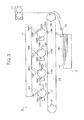
- multiple image forming units 106BK, 106M, 106 C, and 106Y are laid out from upstream of the moving direction of the conveyance belt 105 along with the conveyance belt 105 as an intermediate transfer belt on which an intermediate transfer image to be transferred on paper 104 (an example of a recording medium) fed separately from a paper feed tray 101 by a feediug roller 102 and a separating roller 103 is formed.
- These multiple image forming units 106BK, 106M, 106C, and 106Y have the same inner configuration except the color of the formed toner image.
- the image forming unit 106BK forms a black image
- the image forming unit 106M forms a magenta image
- the image forming unit 106C forms a cyan image
- the image forming unit 106Y forms a yellow image.
- the conveyance belt 105 is an endless moving belt that runs between a driving roller 107 and a driven roller 108.
- a driving motor (not shown in figures) drives the driving roller 107.
- the conveyance belt 105 is moved endlessly by the driving motor, the driving roller 107, and the driven roller 108.
- the image forming unit 106BK transfers a black toner image firstly on the driven conveyance belt 105.
- the image forming unit 106BK includes a photoconductor drum 109BK, a charging unit 110BK laid out surrounding of the photoconductor drum 109BK, an optical writing unit 200, a developing unit 112BK, a photoconductor cleaner (not shown in figures), and a neutralizing unit 113BK etc.
- the optical writing unit 200 is configured to illuminate on each photoconductor drum 109BK, 109M, 109C, and 109Y (hereinafter referred to as photoconductor drum 109 collectively) laid out surrounding of the photoconductor drum 109BK.
- the charging unit 110BK charges the outer surface of the photoconductor drum 109BK uniformly in the dark
- light emitted from the light source corresponding to black image in the optical writing unit 200 executes drawing on the outer surface of the photoconductor drum 109BK, and an electrostatic latent image is formed.
- the developing unit 112BK visualizes the electrostatic latent image using the black toner, and the black toner image is formed on the photoconductor drum 109BK.
- This toner image is transferred on the conveyance belt 105 by the transferring unit 115BK at the position where the photoconductor drum 109BK contacts the conveyance belt 105 or the photoconductor drum 109BK gets close to the conveyance belt 105 most (the transferring position).
- This transfer forms an image by black toner on the conveyance belt 105.
- a photoconductor cleaner cleans remaining waste toner on the outer surface of the photoconductor drum 109BK.
- the photoconductor drum 109BK is neutralized by the neutralizing unit 113BK and waits for forming a subsequent image.
- the black toner image transferred to the surface of the conveyance belt 105 by the image forming unit 106BK is carried to the subsequent image forming unit 106M by the roller that moves the conveyance belt 105.
- a magenta toner image is formed on the photoconductor drum 109M by the same image forming process as in the image forming unit 106BK, and the magenta toner image is superimposed on the black toner image formed previously and transferred.
- the black toner image and the magenta toner image transferred to the surface of the conveyance belt 105 are carried to subsequent image forming units 106C and 106Y, and a cyan toner image formed on the photoconductor drum 109C and a yellow toner image formed on the photoconductor drum 109Y are superimposed on the existing toner images respectively and transferred in the same way. Consequently, a full-color intermediate transfer image is formed on the conveyance belt 105.
- the uppermost paper 104 stored in the paper feed tray 101 is fed sequentially, one sheet at a time, and the intermediate transfer image formed on the conveyance belt 105 is transferred to the surface of the paper at the position where the paper carrying path contacts the conveyance belt 105 or the paper carrying path comes closest to the conveyance belt 105. Consequently, an image is formed on the surface of the paper 104.
- the paper 104 is further conveyed to the fixing unit 116, which fixes the image on the surface of the paper 104, and the paper 104 is then ejected to the outside of the image forming apparatus 1.
- optical writing unit 111 in this embodiment will be described below.
- FIG. 4 is a diagram illustrating relative positions of the optical writing unit 111 and the photoconductor drum 109 in this embodiment.
- LEDA Light-emitting Diode Arrays
- FIG. 4 Light-emitting Diode Arrays 130BK, 130M, 130C, and 130Y (hereinafter collectively referred to as "LEDA 130") as light sources illuminate a respective one of the photoconductor drum 109BK, 109M, 109C, and 109Y
- the LEDA 130 is configured in the way that Light-emitting Diodes (LEDs) as illuminating devices are laid side-by-side in the main scanning direction of the photoconductor drum 109.
- a controller included in the optical writing unit 111 controls turning on and off each LED laid side-by-side in the main scanning direction for each main scanning line based on the drawing data input from the controller 20, exposes the surface of the photoconductor drum 109 selectively, and forms the electrostatic latent image.
- FIG. 5 is a diagram illustrating a functional configuration of the optical writing unit controller 120 that controls the optical writing unit 111 and connecting relationship with the LEDA 130 in this embodiment.
- the optical writing unit controller 120 in this embodiment includes a drawing data acquisition unit 121, a light emitting controller 122, an emission time controller 123, and a resolution controller 124, and functions as an optical writing controller that controls the LEDA 130 as the light source.
- the LEDA 130 includes a data storing unit 131.
- the data storing unit 131 stores information that indicates luminous efficiency for each LEDA 130 (hereinafter referred to as "luminous efficiency information").
- the luminous efficiency information means exposure intensity acquired by having the LEDA 130 emit continuously for a predefined time, that is, amount of exposure energy acquired by exposing for a predefined exposure time, and is shown in units of watts (W) in this embodiment.
- the optical writing unit 111 includes information processing units such as the CPU 10, the RAM 11, the ROM 12, and the HDD 14, etc., shown in FIG. 1 .
- the optical writing unit controller 120 is configured by loading control programs stored in the ROM 12 or the HDD 14 into the RAM 11 and operating by the CPU 10 in accordance with the programs just like as the controller 20 in the image forming apparatus 1.
- the drawing data acquisition unit 121 acquires drawing data input from the engine controller 31 in the controller 20, that is, data for each pixel that comprises an image to be formed and output.
- the light emitting controller 122 controls the LEDA 130 emitting light for each line period in accordance with a signal that indicates the line period (hereinafter referred to as "horizontal synchronizing signal") input from the engine controller 31 and based on the drawing data acquired by the drawing data acquisition unit 121.
- the resolution controller 123 recognizes resolution of the latent image that the optical writing unit controller 120 forms on the photoconductor controlling the LEDA 130 based on the control signal input from the engine controller 31 in the controller 20. After recognizing the resolution, the resolution controller 123 determines amount of light emission per one line period (hereinafter referred to as "requisite amount of light") based on the recognized resolution. Also, the resolution controller 123 determines length of one line period based on the recognized resolution.
- the emission time controller 124 controls emission time when the light emitting controller 122 controls emitting of the LEDA 130.
- the emission time controller 124 controls emitting period of the LEDA 130 in one line period (i.e., strobe time) based on the requisite amount of light determined by the resolution controller 123 and the luminous efficiency information acquired from the data storing unit 131. in the LEDA 130.
- the emission time controller 124 determines limit value of strobe time allowable in one line period based on the one line period length determined by the resolution controller 123.
- the optical writing unit 111 an electrostatic latent image in accordance with an image for one line is formed for each line period by illuminating the LEDA 130. Therefore, strobe time in one line period needs to be less than one line period length.
- the emission time controller 124 can detect such irregular cases.
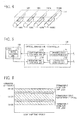
- FIG. 6 is a diagram illustrating a difference range of luminous efficiency allowable among different LEDA 130 and a difference range of luminous efficiency allowable among multiple light emitting devices included in one LEDA 130.
- the difference range of luminous efficiency allowable among different LEDA 130 is between 1.0W and 3.0W. Contrarily, the difference range of luminous efficiency allowable among multiple light emitting devices included in one LEDA 130 is within ⁇ 3%.
- the luminous efficiency of light emitting devices included in LEDA-A is distributed within ⁇ 3% around 2.5W
- the luminous efficiency of light emitting devices included in LEDA-B is distributed within ⁇ 3% around 1.5W.
- each light emitting device is constructed of semiconductors, it is difficult to prevent dispersion of luminous efficiency, and the luminous efficiency is distributed within the range between 1.0W and 3.0W as shown in FIG. 6 . If luminous efficiency of light emitting devices included in one LEDA 130 differs largely, that results in uneven density of the formed image, so difference of luminous efficiency of light emitting devices included in one LEDA 130 is kept within ⁇ 3% as shown in FIG. 6 .
- luminous efficiency of light emitting devices included in different LEDA 130 is distributed between 1.0W and 3.0W as shown in FIG. 6 .
- FIG. 7 is a graph illustrating relationship between emission time and exposure energy regarding two LEDA 130 whose luminous efficiency are different.
- FIG. 7 two charts of 3.0W as the upper limit and 1.0W as the lower limit for permissible zone of luminous efficiency shown in FIG. 6 are illustrated.
- strobe time T to gain desired exposure energy Q can be calculated using luminous efficiency X by following equation (1).
- T Q X
- T 1 Y
- T 2 Y 3
- the emission time controller 124 calculates strobe time T substituting the requisite amount of light acquired from the resolution controller 123 for the exposure energy Y described above and substituting the luminous efficiency information acquired from the data storing unit 131 for the luminous efficiency described above.
- the light emitting controller 122 recognizes line period in accordance with the horizontal synchronizing signal input from the engine controller 31 and controls illuminating for each line period.
- the horizontal synchronizing signal is a period in response to resolution of an image to be formed. Therefore, the information that the emission time controller 124 gives the light emitting controller 122 to control strobe time per one line indicates strobe time needed in accordance with the resolution.
- the resolution controller 123 in this embodiment recognizes resolution in forming and outputting an image based on the control signal input from the engine controller 31 and determines requisite amount of light in accordance with the resolution. That specific process will be described below.
- Exposure energy Q V can be defined for each photoconductor drum 109. Exposure energy Q V can be calculated assuming that the unit area is 1cm 2 resolution of forming and outputting an image is D x *D y dpi, and exposure energy required per one dot is Q D by following equation (4).
- Q V Q D ⁇ 2.54 D x ⁇ 2.54 D y
- the exposure energy per one dot Q D is the requisite exposure energy for each light emitting device per one line period and is used as exposure intensity per pixel.
- the resolution controller 123 functions as exposure intensity calculating unit per pixel. Therefore, strobe time T to gain desired exposure energy can be calculated substituting Q D in the equation (4) for Q in the equation (1) by following equation (5).
- T Q V X ⁇ D x 2.54 ⁇ D y 2.54
- the resolution controller 123 in this embodiment calculates the exposure energy per one dot Q D as the requisite amount of light using D x and D y acquired from the engine controller 31 and predefined Q V in accordance with the equation (4) described above and substitute the calculated Q D in the emission time controller 124.
- the emission time controller 124 calculates the strobe time to be input in the light emitting controller 122 using Q D input from the resolution controller 123 and X acquired from the data storing unit 131 in accordance with the equation (1) described above. That is, the emission time controller 124 functions as an emission time calculating unit that calculates line period emission time in which the LEDA 130 illuminates in one line period.
- the optical writing unit controller 120 in this embodiment it is possible to execute forming and outputting an image with suitable density correcting errors in luminous efficiency of the LEDA 130 regardless of resolution for forming and outputting an image.
- the resolution controller 123 calculates the requisite amount of light in accordance with the equation (4), and the emission time controller 124 calculates the strobe time in accordance with the equation (2) was taken as an example and described above in this embodiment.
- a module that functions as both the resolution controller 123 and the emission time controller 124 can calculate the strobe time in accordance with the equation (5) directly based on requisite exposure energy per unit area Q v , resolution, and luminous efficiency information X in other embodiments.
- the case in which the light emitting controller 122 controls emitting of the LEDA 130 in accordance with the strobe time calculated by the emission time controller 124 was taken as an example.
- the calculated strobe time could be longer than the length of one line period (i.e. permissible zone).
- the calculated strobe time could be shorter than the length of the shortest period in which emitting of the LEDA 130 is controllable.
- error of density can be reduced as minimum as possible using the longest period of time permissible within one line period or the shortest period of time in which emitting of the LEDA 130 is controllable as the strobe time.
- the emission time controller 124 matches densities between colors by adjusting the requisite amount of light calculated by the resolution controller 123 if the calculated strobe time exceeds the permissible zone in at least one of the LEDA 130 set up for each color. That process will be described below with reference to a flowchart in FIG. 8 .
- FIG. 8 is a flowchart illustrating a process that the emission time controller 124 executes after acquiring the requisite amount of light from the resolution controller 123 in case of adjusting the requisite amount of light described above. It should be noted that it is premised in the process illustrated in FIG. 8 that the resolution controller 123 notifies the emission time controller 124 of the line period calculated in accordance with the resolution information notified by the engine controller 31 along with the requisite amount of light Q D calculated in accordance with the equation (4). The line period can be calculated based on the moving velocity of the surface of the photoconductor drum 109 due to the rotation and resolution.
- the emission time controller 124 reads the luminous efficiency information from the data storing unit 131 in the chosen LEDA 130 and calculates the strobe time in S802. Subsequently, the emission time controller 124 determines whether or not the calculated strobe time is within the permissible zone in S803.
- the emission time controller 124 determines whether or not it has already finished processing for every LEDA 130 in S804. If it has finished processing for every LEDA 130 (YES in S804), the process ends. Consequently, the emission time controller 124 notifies the light emitting controller 122 of the calculated strobe time. Contrarily, if it has not finished processing yet (NO in S804), it repeats the process from S801 for other LEDA 130.
- the emission time controller 124 adjusts the value of Q D so that the strobe time fits into the permissible zone in accordance with the equation (1) in S805.
- the emission time controller 124 sets the value of Q D so that the strobe time is equal to the upper limit for the value of the permissible zone in accordance with the equation (1) if the calculated strobe time is longer than the upper limit for the value of the permissible zone.
- the emission time controller 124 sets the value of Q D so that the strobe time is equal to the lower limit value of the permissible zone in accordance with the equation (1).
- the emission time controller 124 resets the calculated strobe time for LEDA 130 for each color in S806, and starts processing for LEDA 130 for each color from S801 again.
- the emission time controller 124 adjusts the requisite amount of light Q D so that the strobe time fits into the permissible zone and calculates the strobe time for other LEDA 130 based on the adjusted requisite amount of light Q D .
- the strobe times are adjusted. Therefore, a case in which one color is paler or deeper than other colors that comprise a full-color image is avoidable.
- the line period is determined by inputting a horizontal synchronizing signal into the optical writing unit controller 120 usually, information on resolution and line period are not input into the optical writing unit controller 120. Contrarily, in this embodiment, since the resolution controller 123 acquires the information on the resolution from the engine controller 31, it is possible to calculate the line period based on the information and execute the process shown in FIG. 8 consequently.
- the zone from the shortest period of time in which emitting of the LEDA 130 is controllable to the line period is used as the permissible zone for the strobe time was taken as an example.
- the upper limit for the value of the strobe time can be shorter than the line period to allow a margin.
- the upper limit for the value of the strobe time can be 97%, 95%, or 90% of the line period, or the upper limit for the value of the strobe time can be calculated by subtracting a fixed value such as [line period] - [predefined time].
- the emission time controller 124 can set the strobe time to zero and control the LEDA 130 so that it does not illuminate. Consequently, irregular controls in which irregular values are set to parameters can be avoided.
- the luminous efficiency information stored in the data storing unit 131 in the LEDA 130 indicates luminous efficiency of each LEDA 130.
- the LEDA 130 includes a plurality of light emitting devices, and the plurality of light emitting devices included in one LEDA 130 have a margin of error in luminous efficiency up to ⁇ 3% at a maximum as described above with reference to FIG. 6 .
- luminous efficiency information stored in the data storing unit 131 can be considered.
- a representative value calculated by processing the multiple luminous efficiency values for each light emitting device included in the LEDA 130 statistically can be stored in the data storing unit 131 in one embodiment.
- the emission time controller 124 can use the representative value in calculating the equation (1) directly.
- luminous efficiency values for each of the multiple light emitting devices included in the LEDA 130 can be stored in the data storing unit 131.
- the emission time controller 124 can use the value calculated by processing statistically or averaging the luminous efficiency values for the value of X in the equation (1).
- the emission time controller 124 can calculate strobe time based on luminous efficiency information for each of the light emitting devices included in the data storing unit 131 and notify the light emitting controller 122 of the strobe time values corresponding to each of the light emitting devices.
- the emission time controller 124 can use the value calculated by processing statistically or averaging the luminous efficiency values of the light emitting devices included in each group for the value of X in the equation (1). Consequently, the emission time controller 124 can notify the light emitting controller 122 of suitable strobe time for each group.
- the emission time can be controlled preferably by optimizing calculation of the strobe time in accordance with the format of the luminous efficiency information stored in the data storing unit 131 in the LEDA 130 and the emission control of the LEDA 130 by the light emitting controller 122.
- the emission time controller 124 calculates the strobe time based on the requisite amount of light notified by the resolution controller 123 and the luminous efficiency information acquired from the data storing unit 131 is described.
- the emission time controller 124 can calculate the strobe time considering adjusting and controlling such aging deterioration.
- the emission time controller 124 adjusts X in the equation (1) to reflect the deterioration of the luminous efficiency. Consequently, the strobe time can be calculated reflecting the adjusted value in accordance with the aging deterioration.
- the optical writing unit controller 120 can include another module that adjust the strobe time calculated by the emission time controller 124 in accordance with the aging deterioration.
- the case in which the LEDA that adopts LEDs as the light emitting devices is used as the light source to expose the photoconductor drum 109 was described as an example.
- the exposure head that adopts the light source other than LED the exposure head whose luminous efficiency data stored in the data storing unit 131 is available can also be used.
- the case in which the LEDA 130 includes the data storing unit 131 is described as an example.
- the resolution controller 123 acquires information on resolution in format of D x *D y (dpi) was described.
- This information on resolution is used to calculate the line period shown in the equation (4) and FIG. 8 . That is, information with which the equation (4) and the line period can be calculated such as information on the number of dots in 1cm 2 or the size of one dot can be used for that purpose.
- the information described above is information on the resolution in forming and outputting an image in either format described above.
- this invention may be implemented as convenient using a conventional general-purpose digital computer programmed according to the teachings of the present specification.
- Appropriate software coding can readily be prepared by skilled programmers based on the teachings of the present disclosure, as will be apparent to those skilled in the software arts.
- the present invention may also be implemented by the preparation of application-specific integrated circuits or by interconnecting an appropriate network of conventional component circuits, as will be readily apparent to those skilled in the relevant art.
Landscapes
- Physics & Mathematics (AREA)
- General Physics & Mathematics (AREA)
- Printers Or Recording Devices Using Electromagnetic And Radiation Means (AREA)
- Control Or Security For Electrophotography (AREA)
- Exposure Or Original Feeding In Electrophotography (AREA)
Abstract
Description
- The present invention relates to an optical writing controller, an image forming apparatus, and an optical writing control method that facilitate controlling light emission time of a light source.
- With increasing digitization of information, image processing apparatuses such as printers and facsimiles for outputting digitized information and scanners for digitizing documents have become indispensable. Usually, such image processing apparatuses are configured as a multi functional peripheral that can be used as a printer, a facsimile, a scanner, and a copier including capabilities such as an image pickup capability, an image forming capability, and a communication capability.
- Among such image processing apparatuses, electrophotographic image forming apparatuses are generally used for outputting digitized documents. In an electrophotographic image forming apparatus, an electrostatic latent image is formed by exposing a photoconductor, a toner image is formed by developing the electrostatic latent image with a developer such as toner, and a paper printout is output after transferring the toner image onto the paper.
- In the electrophotographic image forming apparatuses described above, an image to be output is divided into a plurality of lines, and an optical writing unit forms an image for each line by exposing the photoconductor selectively in accordance with pixels that comprise each line. In some cases, a Light-emitting diode Print Head (LPH) is used as a light source for the optical writing unit described above.
- If the strength of the light source is deteriorating, a technique of adjusting the exposure time in response to the decreasing amount of emitted light has been proposed (e.g.,
JP-2004-191459-A - In the technology described in
JP-2004-191459-A JP-2004-191459-A - The present invention provides a novel optical writing unit, an image forming apparatus, and an optical writing control method that correct idiosyncrasy among exposure heads and enable formation and output of images with constant density regardless of resolution.
- More specifically, an embodiment of the present invention provides an optical writing controller that controls a light source to expose a photoconductor, forms an electrostatic latent image on the photoconductor, and includes an exposure intensity calculator that calculates exposure intensity per pixel based on requisite exposure intensity per unit area on the photoconductor and information on resolution after acquiring information on resolution of the electrostatic latent image, an emission time calculator that calculates line period emission time in which the light source emits light per one line period based on the calculated exposure intensity per pixel and information on luminous efficiency after acquiring information on luminous efficiency as exposure intensity in case of emitting the light source for predefined period, and a light emitting controller that controls emitting of the light source based on the calculated line period emission time.
- Another embodiment of the present invention provides an image forming apparatus that includes the optical writing controller described above.
- A more complete appreciation of the disclosure and many of the attendant advantages thereof will be readily obtained as the same becomes better understood by reference to the following detailed description when considered in conjunction with the accompanying drawings.
-
FIG. 1 is a block diagram illustrating a hardware configuration of an image forming apparatus as an embodiment. -
FIG. 2 is a diagram illustrating a functional configuration of the image forming apparatus. -
FIG. 3 is a diagram illustrating a configuration of a print engine. -
FIG. 4 is a diagram illustrating a configuration of an optical writing unit. -
FIG. 5 is a block diagram illustrating a configuration of an optical writing controller and a (Light-emitting Diode Array) LEDA. -
FIG. 6 is a diagram illustrating an example of luminous efficiency of the LEDAs. -
FIG. 7 is a graph illustrating the relationship between emission time and exposure energy of the LEDAs. -
FIG. 8 is a flowchart illustrating a process that an emission time controller executes. - In describing preferred embodiments illustrated in the drawings, specific terminology is employed for the sake of clarity. However, the disclosure of this patent specification is not intended to be limited to the specific terminology so selected, and it is to be understood that each specific element includes all technical equivalents that have the same function, operate in a similar manner, and achieve a similar result.
- Embodiments of the present invention will be described in detail below with reference to the drawings. In the embodiments of the present invention, a Multi Functional Peripheral (MFP) is taken as an example of an image forming apparatus. The image forming apparatus in the embodiments of the present invention adopts electrophotographic technology, and a main issue of the present invention is to correct idiosyncrasy among exposure heads that include a light emitting device to expose a photoconductor.
-
FIG. 1 is a block diagram illustrating a hardware configuration of an image forming apparatus as an embodiment. As shown inFIG. 1 , animage forming apparatus 1 in this embodiment includes an engine to execute forming images in addition to the same configuration as an information processing terminal such as a standard server and a personal computer (PC). That is, in theimage forming apparatus 1, a Central Processing Unit (CPU) 10, a Random Access Memory (RAM) 11, a Read Only Memory (ROM) 12, an engine 13, a Hard Disk Drive (HDD) 14, and an I/F 15 are connected with each other via abus 18. Also, a Liquid Crystal Display (LCD) 16 and anoperating device 17 are connected to the I/F 15. - The
CPU 10 controls the whole operation of theimage forming apparatus 1. TheRAM 11 is a volatile storage device that information can be written to and read at high speed, and used as a working area when theCPU 10 processes information. TheROM 12 is a read-only nonvolatile storage device and stores programs such as firmware. The engine 13 executes forming an image in theimage forming apparatus 1. - The
HDD 14 is a nonvolatile storage device that information can be written to and read and stores an Operating System (OS), various control programs, and application programs etc. The I/F 15 connects thebus 18 to various hardware and networks and controls them. TheLCD 16 is a visual interface to check the status of theimage forming apparatus 1. Theoperating device 17 is a user interface such as a keyboard and a mouse to input information into theimage forming apparatus 1. - In the hardware configuration described above, programs stored in the
ROM 12, theHDD 14, and storage devices such as optical disks (not shown in figures) are read and loaded into theRAM 11, and software control units are configured by theCPU 10's executing calculation in accordance with those programs. Functional blocks to implement functions of theimage forming apparatus 1 in this embodiment are configured in combination with the software control units described above and the hardware. - Next, a functional configuration of the
image forming apparatus 1 in this embodiment will be described below with reference toFIG. 2. FIG. 2 is a diagram illustrating the functional configuration of theimage forming apparatus 1 in this embodiment. As shown inFIG. 2 , theimage forming apparatus 1 in this embodiment includes acontroller 20, an Auto Document Feeder (ADF) 110, ascanner unit 22, apaper output tray 23, adisplay panel 24, a paper feed table 25, aprinter engine 26, apaper output tray 27, and a network I/F 28. - Also, the
controller 20 includes amain controller 30, anengine controller 31, an input/output controller 32, animage processor 33, and anoperation display controller 34. As shown inFIG. 2 , theimage forming apparatus 1 is configured as a MFP that includes thescanner unit 22 and theprinter engine 26. It should be noted that solid arrows show electrical connections, and dotted arrows show the flow of paper. - The
display panel 24 is an output interface to display the status of theimage forming apparatus 1 visually and an input interface (operating device) to operate theimage forming apparatus 1 directly and input information to theimage forming apparatus 1 as a touch panel. The network I/F 28 is an interface for theimage forming apparatus 1 to communicate with other apparatuses via the network, and Ethernet and USB I/F are adopted as the network I/F 28. - The
controller 20 is configured comprising software and hardware. More particularly, control programs such as firmware stored in the nonvolatile storage device such as theROM 12, theHDD 14, and the optical disks etc. are loaded into the volatile memory (hereinafter referred to as "memory") such as theRAM 11, and thecontroller 20 is configured with software control units implemented by operation of theCPU 10 in accordance with the programs and hardware such as integrated circuits. Thecontroller 20 functions as a control unit that controls the wholeimage forming apparatus 1. - The
main controller 30 controls and commands each unit included in thecontroller 20. The engine controller 31 controls and drives theprinter engine 26 and thescanner unit 22 etc. The input/output controller 32 inputs signals and commands input via the network I/F 28 into themain controller 30. Also, themain controller 30 controls the input/output controller 32 and accesses other apparatuses via the network I/F 28. - The
image processor 33 generates drawing data based on print data included in an input print job under the control of themain controller 30. The drawing data is information for the printer engine to draw an image to be formed in the image forming operation. Also, the print data included in the print job is image data converted into a format that theimage forming apparatus 1 can recognize by a printer driver installed in an information processing apparatus such as a PC. Theoperation display controller 34 displays information on thedisplay panel 24 and notifies themain controller 30 of information input via thedisplay panel 24. - In case the
image forming apparatus 1 operates as a printer, first, the input/output controller 32 receives a print job via the network I/F 28. The input/output controller 32 transfers the received print job to themain controller 30. After receiving the print job, themain controller 30 controls theimage processor 33 and has theimage processor 33 generate drawing data based on print data included in the print job. - After the
image processor 33 generates the drawing data, theengine controller 31 controls theprinter engine 26 based on the generated drawing data and executes forming an image on paper conveyed from the paper feed table 25. That is, theprinter engine 26 functions as an image forming unit. After the printer engine forms the image on the paper, a document is ejected on thepaper output tray 27. - In case the
image forming apparatus 1 operates as a scanner, theoperation display controller 34 or the input/output controller 32 transfers a signal to execute scanning to themain controller 30 in accordance with a request to execute scanning input by a user operation on thedisplay panel 24 or input from an external PC etc. via the network I/F 28. Themain controller 30 controls theengine controller 31 based on the received signal to execute scanning. - The
engine controller 31 drives theADF 21 and carries a document to be scanned set on theADF 21 to thescanner unit 22. Also, theengine controller 31 drives thescanner unit 22 and scans the document conveyed from theADF 21. Also, if the document is set on thescanner unit 22 directly instead of being set on theADF 21, thescanner unit 22 scans the set document under the control of theengine controller 31. That is, thescanner unit 22 functions as an image pickup unit. - In the scanning operation, an image pick up device such as a CCD included in the
scanner unit 22 scans the document optically, and scanned data is generated based on the optical information. Theengine controller 31 transfers the scanned data generated by thescanner unit 22 to theimage processor 33. Theimage processor 33 generates image data based on the scanned data received from theengine controller 31 under the control of themain controller 30. The image data generated by theimage processor 33 is stored in the storage device such as the HDD 40, etc., included in theimage forming apparatus 1. That is, thescanner unit 22, theengine controller 31, and theimage processor 33 cooperate and function as a document scanning unit. - Also, in case the
image forming apparatus 1 functions as a copier, theimage processor 33 generates drawing data based on the scanned data that theengine controller 31 received from thescanner unit 22 or the image data that theimage processor 33 generated. Just like the printer operation, theengine controller 31 drives theprinter engine 26 based on the drawing data. - Next, a configuration of the
printer engine 26 in this embodiment will be described below with reference toFIG. 3 . As shown inFIG. 3 , in theprinter engine 26 of this embodiment, image forming units 106 for each color are laid out along with aconveyance belt 105 as an endless transferring unit, and that configuration is so-called tandem type. That is, multiple image forming units 106BK, 106M, 106 C, and 106Y (electrophotographic processing units) are laid out from upstream of the moving direction of theconveyance belt 105 along with theconveyance belt 105 as an intermediate transfer belt on which an intermediate transfer image to be transferred on paper 104 (an example of a recording medium) fed separately from apaper feed tray 101 by afeediug roller 102 and a separatingroller 103 is formed. - These multiple image forming units 106BK, 106M, 106C, and 106Y have the same inner configuration except the color of the formed toner image. The image forming unit 106BK forms a black image, the
image forming unit 106M forms a magenta image, the image forming unit 106C forms a cyan image, and theimage forming unit 106Y forms a yellow image. While an operation of the image forming unit 106BK will be described below specifically, it should be noted that cases for otherimage forming units image forming unit FIG. 3 , and their detailed descriptions are omitted. - The
conveyance belt 105 is an endless moving belt that runs between a drivingroller 107 and a drivenroller 108. A driving motor (not shown in figures) drives the drivingroller 107. Theconveyance belt 105 is moved endlessly by the driving motor, the drivingroller 107, and the drivenroller 108. - In forming an image, the image forming unit 106BK transfers a black toner image firstly on the driven
conveyance belt 105. The image forming unit 106BK includes a photoconductor drum 109BK, a charging unit 110BK laid out surrounding of the photoconductor drum 109BK, an optical writing unit 200, a developing unit 112BK, a photoconductor cleaner (not shown in figures), and a neutralizing unit 113BK etc. The optical writing unit 200 is configured to illuminate on each photoconductor drum 109BK, 109M, 109C, and 109Y (hereinafter referred to as photoconductor drum 109 collectively) laid out surrounding of the photoconductor drum 109BK. - In forming an image, after the charging unit 110BK charges the outer surface of the photoconductor drum 109BK uniformly in the dark, light emitted from the light source corresponding to black image in the optical writing unit 200 executes drawing on the outer surface of the photoconductor drum 109BK, and an electrostatic latent image is formed. The developing unit 112BK visualizes the electrostatic latent image using the black toner, and the black toner image is formed on the photoconductor drum 109BK.
- This toner image is transferred on the
conveyance belt 105 by the transferring unit 115BK at the position where the photoconductor drum 109BK contacts theconveyance belt 105 or the photoconductor drum 109BK gets close to theconveyance belt 105 most (the transferring position). This transfer forms an image by black toner on theconveyance belt 105. After transferring the toner image, a photoconductor cleaner cleans remaining waste toner on the outer surface of the photoconductor drum 109BK. Subsequently, the photoconductor drum 109BK is neutralized by the neutralizing unit 113BK and waits for forming a subsequent image. - As described above, the black toner image transferred to the surface of the
conveyance belt 105 by the image forming unit 106BK is carried to the subsequentimage forming unit 106M by the roller that moves theconveyance belt 105. In theimage forming unit 106M, a magenta toner image is formed on thephotoconductor drum 109M by the same image forming process as in the image forming unit 106BK, and the magenta toner image is superimposed on the black toner image formed previously and transferred. - The black toner image and the magenta toner image transferred to the surface of the
conveyance belt 105 are carried to subsequentimage forming units 106C and 106Y, and a cyan toner image formed on thephotoconductor drum 109C and a yellow toner image formed on thephotoconductor drum 109Y are superimposed on the existing toner images respectively and transferred in the same way. Consequently, a full-color intermediate transfer image is formed on theconveyance belt 105. - The
uppermost paper 104 stored in thepaper feed tray 101 is fed sequentially, one sheet at a time, and the intermediate transfer image formed on theconveyance belt 105 is transferred to the surface of the paper at the position where the paper carrying path contacts theconveyance belt 105 or the paper carrying path comes closest to theconveyance belt 105. Consequently, an image is formed on the surface of thepaper 104. After forming the image on the surface of thepaper 104, thepaper 104 is further conveyed to the fixingunit 116, which fixes the image on the surface of thepaper 104, and thepaper 104 is then ejected to the outside of theimage forming apparatus 1. - Next, the
optical writing unit 111 in this embodiment will be described below. -
FIG. 4 is a diagram illustrating relative positions of theoptical writing unit 111 and the photoconductor drum 109 in this embodiment. As shown inFIG. 4 , Light-emitting Diode Arrays (LEDA) 130BK, 130M, 130C, and 130Y (hereinafter collectively referred to as "LEDA 130") as light sources illuminate a respective one of the photoconductor drum 109BK, 109M, 109C, and 109Y - The
LEDA 130 is configured in the way that Light-emitting Diodes (LEDs) as illuminating devices are laid side-by-side in the main scanning direction of the photoconductor drum 109. A controller included in theoptical writing unit 111 controls turning on and off each LED laid side-by-side in the main scanning direction for each main scanning line based on the drawing data input from thecontroller 20, exposes the surface of the photoconductor drum 109 selectively, and forms the electrostatic latent image. -
FIG. 5 is a diagram illustrating a functional configuration of the opticalwriting unit controller 120 that controls theoptical writing unit 111 and connecting relationship with theLEDA 130 in this embodiment. - As shown in
FIG. 5 , the opticalwriting unit controller 120 in this embodiment includes a drawingdata acquisition unit 121, alight emitting controller 122, anemission time controller 123, and aresolution controller 124, and functions as an optical writing controller that controls theLEDA 130 as the light source. Also, as shown inFIG. 5 , theLEDA 130 includes a data storing unit 131. The data storing unit 131 stores information that indicates luminous efficiency for each LEDA 130 (hereinafter referred to as "luminous efficiency information"). The luminous efficiency information means exposure intensity acquired by having theLEDA 130 emit continuously for a predefined time, that is, amount of exposure energy acquired by exposing for a predefined exposure time, and is shown in units of watts (W) in this embodiment. - Also, the
optical writing unit 111 includes information processing units such as theCPU 10, theRAM 11, theROM 12, and theHDD 14, etc., shown inFIG. 1 . The opticalwriting unit controller 120 is configured by loading control programs stored in theROM 12 or theHDD 14 into theRAM 11 and operating by theCPU 10 in accordance with the programs just like as thecontroller 20 in theimage forming apparatus 1. - The drawing
data acquisition unit 121 acquires drawing data input from theengine controller 31 in thecontroller 20, that is, data for each pixel that comprises an image to be formed and output. Thelight emitting controller 122 controls theLEDA 130 emitting light for each line period in accordance with a signal that indicates the line period (hereinafter referred to as "horizontal synchronizing signal") input from theengine controller 31 and based on the drawing data acquired by the drawingdata acquisition unit 121. - The
resolution controller 123 recognizes resolution of the latent image that the opticalwriting unit controller 120 forms on the photoconductor controlling theLEDA 130 based on the control signal input from theengine controller 31 in thecontroller 20. After recognizing the resolution, theresolution controller 123 determines amount of light emission per one line period (hereinafter referred to as "requisite amount of light") based on the recognized resolution. Also, theresolution controller 123 determines length of one line period based on the recognized resolution. - The
emission time controller 124 controls emission time when thelight emitting controller 122 controls emitting of theLEDA 130. Theemission time controller 124 controls emitting period of theLEDA 130 in one line period (i.e., strobe time) based on the requisite amount of light determined by theresolution controller 123 and the luminous efficiency information acquired from the data storing unit 131. in theLEDA 130. - Also, the
emission time controller 124 determines limit value of strobe time allowable in one line period based on the one line period length determined by theresolution controller 123. In theoptical writing unit 111, an electrostatic latent image in accordance with an image for one line is formed for each line period by illuminating theLEDA 130. Therefore, strobe time in one line period needs to be less than one line period length. - Contrarily, if luminous efficiency indicated by the luminous efficiency information acquired from the data storing unit 131 is very low, very long strobe time is required to fulfill the light emission amount determined by the
resolution controller 123, and the calculated strobe time can be longer than one line period length. Theemission time controller 124 can detect such irregular cases. - Luminous efficiency of the
LEDA 130 will be described below.FIG. 6 is a diagram illustrating a difference range of luminous efficiency allowable amongdifferent LEDA 130 and a difference range of luminous efficiency allowable among multiple light emitting devices included in oneLEDA 130. - As shown in
FIG. 6 , the difference range of luminous efficiency allowable amongdifferent LEDA 130 is between 1.0W and 3.0W. Contrarily, the difference range of luminous efficiency allowable among multiple light emitting devices included in oneLEDA 130 is within ±3%. For example, inFIG. 6 , the luminous efficiency of light emitting devices included in LEDA-A is distributed within ±3% around 2.5W, and the luminous efficiency of light emitting devices included in LEDA-B is distributed within ±3% around 1.5W. - Since each light emitting device is constructed of semiconductors, it is difficult to prevent dispersion of luminous efficiency, and the luminous efficiency is distributed within the range between 1.0W and 3.0W as shown in
FIG. 6 . If luminous efficiency of light emitting devices included in oneLEDA 130 differs largely, that results in uneven density of the formed image, so difference of luminous efficiency of light emitting devices included in oneLEDA 130 is kept within ±3% as shown inFIG. 6 . - Contrarily, in trying to keep difference range of luminous efficiency of light emitting devices included in
different LEDA 130 within ±3%, it is necessary to choose suitable devices, and that results in raising manufacturing cost and lowering yield ratio. Therefore, luminous efficiency of light emitting devices included indifferent LEDA 130 is distributed between 1.0W and 3.0W as shown inFIG. 6 . -
FIG. 7 is a graph illustrating relationship between emission time and exposure energy regarding twoLEDA 130 whose luminous efficiency are different. InFIG. 7 , two charts of 3.0W as the upper limit and 1.0W as the lower limit for permissible zone of luminous efficiency shown inFIG. 6 are illustrated. Here, strobe time T to gain desired exposure energy Q can be calculated using luminous efficiency X by following equation (1).
- Therefore, if luminous efficiency is 1.0, strobe time T1 to gain desired exposure energy Y can be calculated by following equation (2).

- Also, if luminous efficiency is 3.0, strobe time T2 to gain desired exposure energy Y can be calculated by following equation (3).

- As described above, even if luminous efficiency varies among
different LEDA 130, it is possible to gain exposure energy at the same level by controlling strobe time. That is, theemission time controller 124 calculates strobe time T substituting the requisite amount of light acquired from theresolution controller 123 for the exposure energy Y described above and substituting the luminous efficiency information acquired from the data storing unit 131 for the luminous efficiency described above. - As described above, the
light emitting controller 122 recognizes line period in accordance with the horizontal synchronizing signal input from theengine controller 31 and controls illuminating for each line period. The horizontal synchronizing signal is a period in response to resolution of an image to be formed. Therefore, the information that theemission time controller 124 gives thelight emitting controller 122 to control strobe time per one line indicates strobe time needed in accordance with the resolution. - Consequently, as described above, the
resolution controller 123 in this embodiment recognizes resolution in forming and outputting an image based on the control signal input from theengine controller 31 and determines requisite amount of light in accordance with the resolution. That specific process will be described below. - Requisite exposure intensity per unit area to gain desired density regardless of resolution, i.e. exposure energy QV can be defined for each photoconductor drum 109. Exposure energy QV can be calculated assuming that the unit area is 1cm2 resolution of forming and outputting an image is Dx*Dy dpi, and exposure energy required per one dot is QD by following equation (4).

- The exposure energy per one dot QD is the requisite exposure energy for each light emitting device per one line period and is used as exposure intensity per pixel. The
resolution controller 123 functions as exposure intensity calculating unit per pixel. Therefore, strobe time T to gain desired exposure energy can be calculated substituting QD in the equation (4) for Q in the equation (1) by following equation (5).
- The
resolution controller 123 in this embodiment calculates the exposure energy per one dot QD as the requisite amount of light using Dx and Dy acquired from theengine controller 31 and predefined QV in accordance with the equation (4) described above and substitute the calculated QD in theemission time controller 124. - The
emission time controller 124 calculates the strobe time to be input in thelight emitting controller 122 using QD input from theresolution controller 123 and X acquired from the data storing unit 131 in accordance with the equation (1) described above. That is, theemission time controller 124 functions as an emission time calculating unit that calculates line period emission time in which theLEDA 130 illuminates in one line period. - In case of a monochrome image forming apparatus that includes one photoconductor drum 109, calculations described above are executed based on luminous efficiency information read from the data storing unit 131 for one
LEDA 130 equipped in accordance with one photoconductor drum 109. - Contrarily, in case of a full-color image forming apparatus that includes multiple photoconductor drums 109 as shown in
FIG. 4 , calculations described above are executed based on luminous efficiency information read from the data storing unit 131 for eachLEDA 130 equipped in accordance with each photoconductor drum 109. Consequently, error of density among multiple colors can be corrected, and quality of an image to be formed and output can be kept high. - As described above, in the optical
writing unit controller 120 in this embodiment, it is possible to execute forming and outputting an image with suitable density correcting errors in luminous efficiency of theLEDA 130 regardless of resolution for forming and outputting an image. - It should be noted that the case in which the
resolution controller 123 calculates the requisite amount of light in accordance with the equation (4), and theemission time controller 124 calculates the strobe time in accordance with the equation (2) was taken as an example and described above in this embodiment. Other than that, a module that functions as both theresolution controller 123 and theemission time controller 124 can calculate the strobe time in accordance with the equation (5) directly based on requisite exposure energy per unit area Qv, resolution, and luminous efficiency information X in other embodiments. - Also, in the embodiment described above, the case in which the
light emitting controller 122 controls emitting of theLEDA 130 in accordance with the strobe time calculated by theemission time controller 124 was taken as an example. However, as described above, in case the luminous efficiency indicated by the luminous efficiency information acquired from the data storing unit 131 is very low, the calculated strobe time could be longer than the length of one line period (i.e. permissible zone). Contrarily, in case the luminous efficiency is very high, the calculated strobe time could be shorter than the length of the shortest period in which emitting of theLEDA 130 is controllable. - In that case, in case of the monochrome image forming apparatuses described above, error of density can be reduced as minimum as possible using the longest period of time permissible within one line period or the shortest period of time in which emitting of the
LEDA 130 is controllable as the strobe time. - On the other hand, in case of the full-color image forming apparatuses, the
emission time controller 124 matches densities between colors by adjusting the requisite amount of light calculated by theresolution controller 123 if the calculated strobe time exceeds the permissible zone in at least one of theLEDA 130 set up for each color. That process will be described below with reference to a flowchart inFIG. 8 . -
FIG. 8 is a flowchart illustrating a process that theemission time controller 124 executes after acquiring the requisite amount of light from theresolution controller 123 in case of adjusting the requisite amount of light described above. It should be noted that it is premised in the process illustrated inFIG. 8 that theresolution controller 123 notifies theemission time controller 124 of the line period calculated in accordance with the resolution information notified by theengine controller 31 along with the requisite amount of light QD calculated in accordance with the equation (4). The line period can be calculated based on the moving velocity of the surface of the photoconductor drum 109 due to the rotation and resolution. - As shown in
FIG. 8 , after choosing oneLEDA 130 in S801, theemission time controller 124 reads the luminous efficiency information from the data storing unit 131 in the chosenLEDA 130 and calculates the strobe time in S802. Subsequently, theemission time controller 124 determines whether or not the calculated strobe time is within the permissible zone in S803. - After the determination in S803, if the strobe time is less than the line period (YES in S803), the
emission time controller 124 determines whether or not it has already finished processing for everyLEDA 130 in S804. If it has finished processing for every LEDA 130 (YES in S804), the process ends. Consequently, theemission time controller 124 notifies thelight emitting controller 122 of the calculated strobe time. Contrarily, if it has not finished processing yet (NO in S804), it repeats the process from S801 forother LEDA 130. - On the other hand, if the strobe time is longer than the line period (NO in S803), the
emission time controller 124 adjusts the value of QD so that the strobe time fits into the permissible zone in accordance with the equation (1) in S805. In S805, theemission time controller 124 sets the value of QD so that the strobe time is equal to the upper limit for the value of the permissible zone in accordance with the equation (1) if the calculated strobe time is longer than the upper limit for the value of the permissible zone. Contrarily, if the calculated strobe time is shorter than the lower limit for the value of the permissible zone, theemission time controller 124 sets the value of QD so that the strobe time is equal to the lower limit value of the permissible zone in accordance with the equation (1). - Subsequently, the
emission time controller 124 resets the calculated strobe time forLEDA 130 for each color in S806, and starts processing forLEDA 130 for each color from S801 again. - As described above, if at least one of the calculated strobe times for one of the
LEDA 130 for each color is longer or shorter than the permissible zone, theemission time controller 124 adjusts the requisite amount of light QD so that the strobe time fits into the permissible zone and calculates the strobe time forother LEDA 130 based on the adjusted requisite amount of light QD. - By executing the process shown in
FIG. 8 , if at least one of the strobe times is longer or shorter than the permissible zone in the full-color image forming apparatus, after adjusting the requisite amount of light in accordance with theLEDA 130, the strobe times forother LEDA 130 are adjusted. Therefore, a case in which one color is paler or deeper than other colors that comprise a full-color image is avoidable. - Since the line period is determined by inputting a horizontal synchronizing signal into the optical
writing unit controller 120 usually, information on resolution and line period are not input into the opticalwriting unit controller 120. Contrarily, in this embodiment, since theresolution controller 123 acquires the information on the resolution from theengine controller 31, it is possible to calculate the line period based on the information and execute the process shown inFIG. 8 consequently. - In the above description for
FIG. 8 , the zone from the shortest period of time in which emitting of theLEDA 130 is controllable to the line period is used as the permissible zone for the strobe time was taken as an example. In another embodiment, the upper limit for the value of the strobe time can be shorter than the line period to allow a margin. In this case, the upper limit for the value of the strobe time can be 97%, 95%, or 90% of the line period, or the upper limit for the value of the strobe time can be calculated by subtracting a fixed value such as [line period] - [predefined time]. - Also, if the calculated strobe time is longer or shorter than the permissible zone as described above, the
emission time controller 124 can set the strobe time to zero and control theLEDA 130 so that it does not illuminate. Consequently, irregular controls in which irregular values are set to parameters can be avoided. - Also, in the embodiment described above, the luminous efficiency information stored in the data storing unit 131 in the
LEDA 130 indicates luminous efficiency of eachLEDA 130. In this case, theLEDA 130 includes a plurality of light emitting devices, and the plurality of light emitting devices included in oneLEDA 130 have a margin of error in luminous efficiency up to ±3% at a maximum as described above with reference toFIG. 6 . - Therefore, various aspects for the luminous efficiency information stored in the data storing unit 131 can be considered. For example, a representative value calculated by processing the multiple luminous efficiency values for each light emitting device included in the
LEDA 130 statistically can be stored in the data storing unit 131 in one embodiment. In this case, theemission time controller 124 can use the representative value in calculating the equation (1) directly. - In another embodiment, luminous efficiency values for each of the multiple light emitting devices included in the
LEDA 130 can be stored in the data storing unit 131. In this case, theemission time controller 124 can use the value calculated by processing statistically or averaging the luminous efficiency values for the value of X in the equation (1). - On the other hand, if emitting of multiple light emitting devices included in the
LEDA 130 can be controlled separately, theemission time controller 124 can calculate strobe time based on luminous efficiency information for each of the light emitting devices included in the data storing unit 131 and notify thelight emitting controller 122 of the strobe time values corresponding to each of the light emitting devices. - Furthermore; if the plurality of the light emitting devices included in the
LEDA 130 can be divided into multiple groups and emitting of the light emitting devices can be controlled for each group separately, theemission time controller 124 can use the value calculated by processing statistically or averaging the luminous efficiency values of the light emitting devices included in each group for the value of X in the equation (1). Consequently, theemission time controller 124 can notify thelight emitting controller 122 of suitable strobe time for each group. - As described above, the emission time can be controlled preferably by optimizing calculation of the strobe time in accordance with the format of the luminous efficiency information stored in the data storing unit 131 in the
LEDA 130 and the emission control of theLEDA 130 by thelight emitting controller 122. - Also, in the above embodiment, the case in which the
emission time controller 124 calculates the strobe time based on the requisite amount of light notified by theresolution controller 123 and the luminous efficiency information acquired from the data storing unit 131 is described. Other than that, regarding the control of the strobe time, it can be controlled adjusting in accordance with the aging deterioration of theLEDA 130. Therefore, theemission time controller 124 can calculate the strobe time considering adjusting and controlling such aging deterioration. - If the aging deterioration of the
LEDA 130 is reflected on adjusting and controlling the strobe time, theemission time controller 124 adjusts X in the equation (1) to reflect the deterioration of the luminous efficiency. Consequently, the strobe time can be calculated reflecting the adjusted value in accordance with the aging deterioration. Other than that, the opticalwriting unit controller 120 can include another module that adjust the strobe time calculated by theemission time controller 124 in accordance with the aging deterioration. - Also, in the above embodiment, the case in which the LEDA that adopts LEDs as the light emitting devices is used as the light source to expose the photoconductor drum 109 was described as an example. In another example, with an exposure head that adopts the light source other than LED, the exposure head whose luminous efficiency data stored in the data storing unit 131 is available can also be used.
- Also, in the above embodiment, the case in which the
LEDA 130 includes the data storing unit 131 is described as an example. However, it is possible to implement the configuration and execute the process described above if the luminous efficiency information for eachLEDA 130 is available, so embodiments in which the luminous efficiency information corresponding to eachLEDA 130 is input from theengine controller 31 and the luminous efficiency information corresponding to eachLEDA 130 is stored in a storing unit included in the opticalwriting unit controller 120 are possible. - Also, in the above embodiment, the case in which the
resolution controller 123 acquires information on resolution in format of Dx*Dy (dpi) was described. This information on resolution is used to calculate the line period shown in the equation (4) andFIG. 8 . That is, information with which the equation (4) and the line period can be calculated such as information on the number of dots in 1cm2 or the size of one dot can be used for that purpose. The information described above is information on the resolution in forming and outputting an image in either format described above. - Numerous additional modifications and variations are possible in light of the above teachings. It is therefore to be understood that, within the scope of the appended claims, the disclosure of this patent specification may be practiced otherwise than as specifically described herein.
- As can be appreciated by those skilled in the computer arts, this invention may be implemented as convenient using a conventional general-purpose digital computer programmed according to the teachings of the present specification. Appropriate software coding can readily be prepared by skilled programmers based on the teachings of the present disclosure, as will be apparent to those skilled in the software arts. The present invention may also be implemented by the preparation of application-specific integrated circuits or by interconnecting an appropriate network of conventional component circuits, as will be readily apparent to those skilled in the relevant art.
Claims (9)
- An optical writing controller (120) that controls a light source (130) to expose a photoconductor (109) and forms an electrostatic latent image on the photoconductor (109), comprising:an exposure intensity calculator (123) to acquire information on resolution of the electrostatic latent image and calculate exposure intensity per pixel based on requisite exposure intensity per unit area on the photoconductor (109) and the information on resolution;an emission time calculator (124) to acquire information on luminous efficiency and calculate a line period emission time in which the light source (130) emits light in one line period based on the calculated exposure intensity per pixel and the information on luminous efficiency; anda light emitting controller (122) that controls emitting of the light source (130) based on the calculated line period emission time.
- The optical writing controller (120) according to claim 1, wherein it is determined whether or not the calculated line period emission time is within a permissible zone of the emission time of the light source (130) determined in accordance with the information on resolution,
the light emitting controller (122) is notified of the line period emission time if the calculated line period emission time is within the permissible zone, and
the emission time calculator (124) adjusts the exposure intensity per pixel so that the line period fits into the permissible zone if the calculated line period emission time is outside of the permissible zone. - The optical writing controller (120) according to claim 2, wherein the light emitting controller (122) controls emitting of multiple light sources (130) for each photoconductor (109) to form an electrostatic latent image developed with different colors, and
the emission time calculator (124) adjusts the exposure intensity per pixel so that the line period fits into the permissible zone if at least one of the line period emission times calculated for the multiple light sources (130) and calculates the line period emission time for other light sources (130) based on the adjusted exposure intensity per pixel. - The optical writing controller (120) according to claim 2, wherein the emission time calculator (124) notifies the light emitting controller (122) of the closest value to the calculated line period emission time within the permissible zone if the calculated line period emission time is outside of the permissible zone.
- The optical writing controller (120) according to claim 2, wherein the emission time calculator (124) notifies the light emitting controller (122) of the line period emission time that indicates the emission time is zero if the calculated line period emission time is outside of the permissible zone.
- The optical writing controller (120) according to any one of claims 2 to 5,
wherein the upper limit for the permissible zone is the line period determined in accordance with the information on resolution. - The optical writing controller (120) according to any one of claims 2 to 5,
wherein the upper limit for the permissible zone is shorter than the line period determined in accordance with the information on resolution. - An image forming apparatus (1), comprising the optical writing controller (120) according to any one of claims 1 to 7.
- A method of controlling a light source (130) to expose a photoconductor (109) and forming an electrostatic latent image on the photoconductor (109), comprising the steps of:acquiring information on resolution of the electrostatic latent image;calculating exposure intensity per pixel based on requisite exposure intensity per unit area on the photoconductor (109) and the information on resolution;acquiring information on luminous efficiency as exposure intensity;calculating line period emission time in which the light source (130) emits light in one line period based on the calculated exposure intensity per pixel and the information on luminous efficiency; andcontrolling emitting of the light source (109) based on the calculated line period emission time.
Applications Claiming Priority (1)
| Application Number | Priority Date | Filing Date | Title |
|---|---|---|---|
| JP2012148737A JP6035912B2 (en) | 2012-07-02 | 2012-07-02 | Optical writing control apparatus, image forming apparatus, and optical writing control method |
Publications (2)
| Publication Number | Publication Date |
|---|---|
| EP2682820A2 true EP2682820A2 (en) | 2014-01-08 |
| EP2682820A3 EP2682820A3 (en) | 2018-01-03 |
Family
ID=48700355
Family Applications (1)
| Application Number | Title | Priority Date | Filing Date |
|---|---|---|---|
| EP13173755.3A Withdrawn EP2682820A3 (en) | 2012-07-02 | 2013-06-26 | Optical writing controller, image forming apparatus, and optical writing control method |
Country Status (2)
| Country | Link |
|---|---|
| EP (1) | EP2682820A3 (en) |
| JP (1) | JP6035912B2 (en) |
Families Citing this family (5)
| Publication number | Priority date | Publication date | Assignee | Title |
|---|---|---|---|---|
| US9062794B2 (en) | 2009-07-08 | 2015-06-23 | Fisher Controls International Llc | Locking actuator stem and rod end bearing apparatus for use with fluid valves |
| JP6281341B2 (en) | 2014-03-14 | 2018-02-21 | 株式会社リコー | Image forming apparatus and light emission control method |
| US9746795B2 (en) | 2015-03-16 | 2017-08-29 | Ricoh Company, Ltd. | Optical writing control device, image forming apparatus, and optical writing control method for controlling light emission of a light source |
| JP6631334B2 (en) * | 2016-03-11 | 2020-01-15 | コニカミノルタ株式会社 | Optical writing device and image forming device |
| JP2020001240A (en) * | 2018-06-27 | 2020-01-09 | キヤノン株式会社 | Image forming device |
Citations (1)
| Publication number | Priority date | Publication date | Assignee | Title |
|---|---|---|---|---|
| JP2004191459A (en) | 2002-12-09 | 2004-07-08 | Matsushita Electric Ind Co Ltd | Electrophotographic equipment |
Family Cites Families (6)
| Publication number | Priority date | Publication date | Assignee | Title |
|---|---|---|---|---|
| JPS6310293Y2 (en) * | 1979-08-21 | 1988-03-28 | ||
| US6965393B2 (en) * | 2002-11-11 | 2005-11-15 | Kyocera Mita Corporation | Image forming apparatus |
| JP2004163496A (en) * | 2002-11-11 | 2004-06-10 | Kyocera Mita Corp | Image forming apparatus |
| JP4862526B2 (en) * | 2006-07-18 | 2012-01-25 | 富士ゼロックス株式会社 | Image forming apparatus |
| JP4946943B2 (en) * | 2008-03-28 | 2012-06-06 | ブラザー工業株式会社 | Image forming apparatus |
| JP5428063B2 (en) * | 2010-03-10 | 2014-02-26 | カシオ計算機株式会社 | Exposure apparatus, drive control method thereof, and image forming apparatus |
-
2012
- 2012-07-02 JP JP2012148737A patent/JP6035912B2/en active Active
-
2013
- 2013-06-26 EP EP13173755.3A patent/EP2682820A3/en not_active Withdrawn
Patent Citations (1)
| Publication number | Priority date | Publication date | Assignee | Title |
|---|---|---|---|---|
| JP2004191459A (en) | 2002-12-09 | 2004-07-08 | Matsushita Electric Ind Co Ltd | Electrophotographic equipment |
Also Published As
| Publication number | Publication date |
|---|---|
| JP2014008743A (en) | 2014-01-20 |
| JP6035912B2 (en) | 2016-11-30 |
| EP2682820A3 (en) | 2018-01-03 |
Similar Documents
| Publication | Publication Date | Title |
|---|---|---|
| US8294744B2 (en) | Optical writing device, image forming apparatus, method of controlling optical writing device, and computer program product | |
| US8730288B2 (en) | Optical writing device, image forming apparatus, and correction value information generating method | |
| JP5724628B2 (en) | Optical writing apparatus and image forming apparatus | |
| US8848238B2 (en) | Optical writing control device, image forming apparatus, and optical writing control method for controlling the light emitting timing of a light source | |
| US20140139607A1 (en) | Optical writing device, image forming apparatus, and method of controlling optical writing device | |
| EP2738617B1 (en) | Optical writing control device, image forming apparatus, and method of controlling optical writing device | |
| US9245217B2 (en) | Optical writing device, image forming apparatus, and method for controlling optical writing device | |
| US9036198B2 (en) | Optical-writing control device, image forming apparatus, and method of controlling optical writing device | |
| US8917303B2 (en) | Optical writing device, image forming device, and method of operating the same | |
| US9106861B2 (en) | Method and apparatus for controlling adjustment of image parameters and image formation and an image apparatus including the game | |
| EP2299686A2 (en) | Image Forming Apparatus | |
| JP6035912B2 (en) | Optical writing control apparatus, image forming apparatus, and optical writing control method | |
| US9360792B2 (en) | Optical writing controller, image forming apparatus, and optical writing control method | |
| JP6149581B2 (en) | Optical writing control apparatus, image forming apparatus, and optical writing control method | |
| US8395648B2 (en) | Optical writer, image forming apparatus, and method of controlling optical writer | |
| US8928713B2 (en) | Optical writing device having a correction value information generating unit, image forming apparatus, and method of controlling optical writing device thereof | |
| US9529295B2 (en) | Optical writing control device for reducing driving power of optical writing device | |
| JP6079176B2 (en) | Optical writing control apparatus, image forming apparatus, and optical writing apparatus control method | |
| US9618875B2 (en) | Optical writing control device, image forming apparatus, and method of controlling optical writing device | |
| JP2015168232A (en) | Optical writing control apparatus, image forming apparatus, and optical writing control method | |
| JP2016022732A (en) | Optical writing control apparatus, image formation device and control method for optical writing device | |
| JP2017024332A (en) | Optical writing control apparatus, image forming apparatus, and optical writing control method | |
| JP2017104998A (en) | Optical writing control apparatus, image forming apparatus, and optical writing control method |
Legal Events
| Date | Code | Title | Description |
|---|---|---|---|
| PUAI | Public reference made under article 153(3) epc to a published international application that has entered the european phase |
Free format text: ORIGINAL CODE: 0009012 |
|
| 17P | Request for examination filed |
Effective date: 20130626 |
|
| AK | Designated contracting states |
Kind code of ref document: A2 Designated state(s): AL AT BE BG CH CY CZ DE DK EE ES FI FR GB GR HR HU IE IS IT LI LT LU LV MC MK MT NL NO PL PT RO RS SE SI SK SM TR |
|
| AX | Request for extension of the european patent |
Extension state: BA ME |
|
| PUAL | Search report despatched |
Free format text: ORIGINAL CODE: 0009013 |
|
| AK | Designated contracting states |
Kind code of ref document: A3 Designated state(s): AL AT BE BG CH CY CZ DE DK EE ES FI FR GB GR HR HU IE IS IT LI LT LU LV MC MK MT NL NO PL PT RO RS SE SI SK SM TR |
|
| AX | Request for extension of the european patent |
Extension state: BA ME |
|
| RIC1 | Information provided on ipc code assigned before grant |
Ipc: G03G 15/043 20060101AFI20171129BHEP |
|
| STAA | Information on the status of an ep patent application or granted ep patent |
Free format text: STATUS: THE APPLICATION IS DEEMED TO BE WITHDRAWN |
|
| 18D | Application deemed to be withdrawn |
Effective date: 20180704 |