EP2680377B1 - Method for making a laser module - Google Patents
Method for making a laser module Download PDFInfo
- Publication number
- EP2680377B1 EP2680377B1 EP12174305.8A EP12174305A EP2680377B1 EP 2680377 B1 EP2680377 B1 EP 2680377B1 EP 12174305 A EP12174305 A EP 12174305A EP 2680377 B1 EP2680377 B1 EP 2680377B1
- Authority
- EP
- European Patent Office
- Prior art keywords
- laser
- crystal
- length
- nonlinear crystal
- nonlinear
- Prior art date
- Legal status (The legal status is an assumption and is not a legal conclusion. Google has not performed a legal analysis and makes no representation as to the accuracy of the status listed.)
- Not-in-force
Links
- 238000000034 method Methods 0.000 title claims description 23
- 239000013078 crystal Substances 0.000 claims description 140
- 239000000758 substrate Substances 0.000 claims description 21
- 150000002500 ions Chemical class 0.000 claims description 20
- 239000000395 magnesium oxide Substances 0.000 claims description 13
- CPLXHLVBOLITMK-UHFFFAOYSA-N magnesium oxide Inorganic materials [Mg]=O CPLXHLVBOLITMK-UHFFFAOYSA-N 0.000 claims description 13
- 229910052751 metal Inorganic materials 0.000 claims description 11
- 239000002184 metal Substances 0.000 claims description 11
- 229910052779 Neodymium Inorganic materials 0.000 claims description 10
- QEFYFXOXNSNQGX-UHFFFAOYSA-N neodymium atom Chemical compound [Nd] QEFYFXOXNSNQGX-UHFFFAOYSA-N 0.000 claims description 10
- 230000003287 optical effect Effects 0.000 claims description 9
- 229910052727 yttrium Inorganic materials 0.000 claims description 7
- VWQVUPCCIRVNHF-UHFFFAOYSA-N yttrium atom Chemical compound [Y] VWQVUPCCIRVNHF-UHFFFAOYSA-N 0.000 claims description 7
- AXZKOIWUVFPNLO-UHFFFAOYSA-N magnesium;oxygen(2-) Chemical compound [O-2].[Mg+2] AXZKOIWUVFPNLO-UHFFFAOYSA-N 0.000 claims description 6
- 239000004411 aluminium Substances 0.000 claims description 5
- 229910052782 aluminium Inorganic materials 0.000 claims description 5
- XAGFODPZIPBFFR-UHFFFAOYSA-N aluminium Chemical compound [Al] XAGFODPZIPBFFR-UHFFFAOYSA-N 0.000 claims description 5
- 238000004806 packaging method and process Methods 0.000 claims description 4
- LSGOVYNHVSXFFJ-UHFFFAOYSA-N vanadate(3-) Chemical compound [O-][V]([O-])([O-])=O LSGOVYNHVSXFFJ-UHFFFAOYSA-N 0.000 claims description 4
- 238000004026 adhesive bonding Methods 0.000 claims description 3
- CNEVBWVCXNYGIA-UHFFFAOYSA-N gadolinium(3+);trioxido(oxo)vanadium Chemical compound [Gd+3].[O-][V]([O-])([O-])=O CNEVBWVCXNYGIA-UHFFFAOYSA-N 0.000 claims description 3
- 239000002223 garnet Substances 0.000 claims description 3
- 238000003466 welding Methods 0.000 claims description 3
- 238000010586 diagram Methods 0.000 description 7
- OFHMUASCSJJNNA-JOCHJYFZSA-N bis-napthyl β-ketophosphonic acid Chemical compound C1=CC=C2C([C@H](C(=O)C=3C=C4C=CC=CC4=CC=3)P(O)(=O)O)=CC=CC2=C1 OFHMUASCSJJNNA-JOCHJYFZSA-N 0.000 description 6
- VCZFPTGOQQOZGI-UHFFFAOYSA-N lithium bis(oxoboranyloxy)borinate Chemical compound [Li+].[O-]B(OB=O)OB=O VCZFPTGOQQOZGI-UHFFFAOYSA-N 0.000 description 6
- 229910017502 Nd:YVO4 Inorganic materials 0.000 description 5
- 238000006243 chemical reaction Methods 0.000 description 5
- 239000000463 material Substances 0.000 description 5
- 230000005540 biological transmission Effects 0.000 description 4
- 238000005086 pumping Methods 0.000 description 4
- XUIMIQQOPSSXEZ-UHFFFAOYSA-N Silicon Chemical compound [Si] XUIMIQQOPSSXEZ-UHFFFAOYSA-N 0.000 description 3
- XBJJRSFLZVLCSE-UHFFFAOYSA-N barium(2+);diborate Chemical compound [Ba+2].[Ba+2].[Ba+2].[O-]B([O-])[O-].[O-]B([O-])[O-] XBJJRSFLZVLCSE-UHFFFAOYSA-N 0.000 description 3
- YISOXLVRWFDIKD-UHFFFAOYSA-N bismuth;borate Chemical compound [Bi+3].[O-]B([O-])[O-] YISOXLVRWFDIKD-UHFFFAOYSA-N 0.000 description 3
- GQYHUHYESMUTHG-UHFFFAOYSA-N lithium niobate Chemical compound [Li+].[O-][Nb](=O)=O GQYHUHYESMUTHG-UHFFFAOYSA-N 0.000 description 3
- 230000010287 polarization Effects 0.000 description 3
- WYOHGPUPVHHUGO-UHFFFAOYSA-K potassium;oxygen(2-);titanium(4+);phosphate Chemical compound [O-2].[K+].[Ti+4].[O-]P([O-])([O-])=O WYOHGPUPVHHUGO-UHFFFAOYSA-K 0.000 description 3
- 239000004065 semiconductor Substances 0.000 description 3
- 229910052710 silicon Inorganic materials 0.000 description 3
- 239000010703 silicon Substances 0.000 description 3
- WSMQKESQZFQMFW-UHFFFAOYSA-N 5-methyl-pyrazole-3-carboxylic acid Chemical compound CC1=CC(C(O)=O)=NN1 WSMQKESQZFQMFW-UHFFFAOYSA-N 0.000 description 2
- FOXXZZGDIAQPQI-XKNYDFJKSA-N Asp-Pro-Ser-Ser Chemical compound OC(=O)C[C@H](N)C(=O)N1CCC[C@H]1C(=O)N[C@@H](CO)C(=O)N[C@@H](CO)C(O)=O FOXXZZGDIAQPQI-XKNYDFJKSA-N 0.000 description 2
- RYGMFSIKBFXOCR-UHFFFAOYSA-N Copper Chemical compound [Cu] RYGMFSIKBFXOCR-UHFFFAOYSA-N 0.000 description 2
- VYPSYNLAJGMNEJ-UHFFFAOYSA-N Silicium dioxide Chemical compound O=[Si]=O VYPSYNLAJGMNEJ-UHFFFAOYSA-N 0.000 description 2
- 239000004020 conductor Substances 0.000 description 2
- 229910052802 copper Inorganic materials 0.000 description 2
- 239000010949 copper Substances 0.000 description 2
- 230000001419 dependent effect Effects 0.000 description 2
- 239000003292 glue Substances 0.000 description 2
- 238000004519 manufacturing process Methods 0.000 description 2
- 238000004021 metal welding Methods 0.000 description 2
- 238000013341 scale-up Methods 0.000 description 2
- 239000000126 substance Substances 0.000 description 2
- 229910001369 Brass Inorganic materials 0.000 description 1
- 229910003327 LiNbO3 Inorganic materials 0.000 description 1
- BQCADISMDOOEFD-UHFFFAOYSA-N Silver Chemical compound [Ag] BQCADISMDOOEFD-UHFFFAOYSA-N 0.000 description 1
- 238000003491 array Methods 0.000 description 1
- 239000010951 brass Substances 0.000 description 1
- 238000004140 cleaning Methods 0.000 description 1
- 239000011248 coating agent Substances 0.000 description 1
- 238000000576 coating method Methods 0.000 description 1
- 239000000084 colloidal system Substances 0.000 description 1
- 239000003086 colorant Substances 0.000 description 1
- 230000000694 effects Effects 0.000 description 1
- 238000005516 engineering process Methods 0.000 description 1
- 239000003822 epoxy resin Substances 0.000 description 1
- 230000017525 heat dissipation Effects 0.000 description 1
- 238000005498 polishing Methods 0.000 description 1
- 229920000647 polyepoxide Polymers 0.000 description 1
- 229920005989 resin Polymers 0.000 description 1
- 239000011347 resin Substances 0.000 description 1
- 229910052594 sapphire Inorganic materials 0.000 description 1
- 239000010980 sapphire Substances 0.000 description 1
- 239000000377 silicon dioxide Substances 0.000 description 1
- 229910052709 silver Inorganic materials 0.000 description 1
- 239000004332 silver Substances 0.000 description 1
Images



Classifications
-
- H—ELECTRICITY
- H01—ELECTRIC ELEMENTS
- H01S—DEVICES USING THE PROCESS OF LIGHT AMPLIFICATION BY STIMULATED EMISSION OF RADIATION [LASER] TO AMPLIFY OR GENERATE LIGHT; DEVICES USING STIMULATED EMISSION OF ELECTROMAGNETIC RADIATION IN WAVE RANGES OTHER THAN OPTICAL
- H01S3/00—Lasers, i.e. devices using stimulated emission of electromagnetic radiation in the infrared, visible or ultraviolet wave range
- H01S3/10—Controlling the intensity, frequency, phase, polarisation or direction of the emitted radiation, e.g. switching, gating, modulating or demodulating
- H01S3/106—Controlling the intensity, frequency, phase, polarisation or direction of the emitted radiation, e.g. switching, gating, modulating or demodulating by controlling devices placed within the cavity
- H01S3/108—Controlling the intensity, frequency, phase, polarisation or direction of the emitted radiation, e.g. switching, gating, modulating or demodulating by controlling devices placed within the cavity using non-linear optical devices, e.g. exhibiting Brillouin or Raman scattering
- H01S3/109—Frequency multiplication, e.g. harmonic generation
-
- H—ELECTRICITY
- H01—ELECTRIC ELEMENTS
- H01S—DEVICES USING THE PROCESS OF LIGHT AMPLIFICATION BY STIMULATED EMISSION OF RADIATION [LASER] TO AMPLIFY OR GENERATE LIGHT; DEVICES USING STIMULATED EMISSION OF ELECTROMAGNETIC RADIATION IN WAVE RANGES OTHER THAN OPTICAL
- H01S3/00—Lasers, i.e. devices using stimulated emission of electromagnetic radiation in the infrared, visible or ultraviolet wave range
- H01S3/02—Constructional details
- H01S3/025—Constructional details of solid state lasers, e.g. housings or mountings
-
- H—ELECTRICITY
- H01—ELECTRIC ELEMENTS
- H01S—DEVICES USING THE PROCESS OF LIGHT AMPLIFICATION BY STIMULATED EMISSION OF RADIATION [LASER] TO AMPLIFY OR GENERATE LIGHT; DEVICES USING STIMULATED EMISSION OF ELECTROMAGNETIC RADIATION IN WAVE RANGES OTHER THAN OPTICAL
- H01S3/00—Lasers, i.e. devices using stimulated emission of electromagnetic radiation in the infrared, visible or ultraviolet wave range
- H01S3/005—Optical devices external to the laser cavity, specially adapted for lasers, e.g. for homogenisation of the beam or for manipulating laser pulses, e.g. pulse shaping
- H01S3/0092—Nonlinear frequency conversion, e.g. second harmonic generation [SHG] or sum- or difference-frequency generation outside the laser cavity
-
- H—ELECTRICITY
- H01—ELECTRIC ELEMENTS
- H01S—DEVICES USING THE PROCESS OF LIGHT AMPLIFICATION BY STIMULATED EMISSION OF RADIATION [LASER] TO AMPLIFY OR GENERATE LIGHT; DEVICES USING STIMULATED EMISSION OF ELECTROMAGNETIC RADIATION IN WAVE RANGES OTHER THAN OPTICAL
- H01S3/00—Lasers, i.e. devices using stimulated emission of electromagnetic radiation in the infrared, visible or ultraviolet wave range
- H01S3/02—Constructional details
- H01S3/04—Arrangements for thermal management
- H01S3/0401—Arrangements for thermal management of optical elements being part of laser resonator, e.g. windows, mirrors, lenses
-
- H—ELECTRICITY
- H01—ELECTRIC ELEMENTS
- H01S—DEVICES USING THE PROCESS OF LIGHT AMPLIFICATION BY STIMULATED EMISSION OF RADIATION [LASER] TO AMPLIFY OR GENERATE LIGHT; DEVICES USING STIMULATED EMISSION OF ELECTROMAGNETIC RADIATION IN WAVE RANGES OTHER THAN OPTICAL
- H01S3/00—Lasers, i.e. devices using stimulated emission of electromagnetic radiation in the infrared, visible or ultraviolet wave range
- H01S3/02—Constructional details
- H01S3/04—Arrangements for thermal management
- H01S3/0405—Conductive cooling, e.g. by heat sinks or thermo-electric elements
-
- H—ELECTRICITY
- H01—ELECTRIC ELEMENTS
- H01S—DEVICES USING THE PROCESS OF LIGHT AMPLIFICATION BY STIMULATED EMISSION OF RADIATION [LASER] TO AMPLIFY OR GENERATE LIGHT; DEVICES USING STIMULATED EMISSION OF ELECTROMAGNETIC RADIATION IN WAVE RANGES OTHER THAN OPTICAL
- H01S3/00—Lasers, i.e. devices using stimulated emission of electromagnetic radiation in the infrared, visible or ultraviolet wave range
- H01S3/02—Constructional details
- H01S3/04—Arrangements for thermal management
- H01S3/042—Arrangements for thermal management for solid state lasers
-
- H—ELECTRICITY
- H01—ELECTRIC ELEMENTS
- H01S—DEVICES USING THE PROCESS OF LIGHT AMPLIFICATION BY STIMULATED EMISSION OF RADIATION [LASER] TO AMPLIFY OR GENERATE LIGHT; DEVICES USING STIMULATED EMISSION OF ELECTROMAGNETIC RADIATION IN WAVE RANGES OTHER THAN OPTICAL
- H01S3/00—Lasers, i.e. devices using stimulated emission of electromagnetic radiation in the infrared, visible or ultraviolet wave range
- H01S3/05—Construction or shape of optical resonators; Accommodation of active medium therein; Shape of active medium
- H01S3/08—Construction or shape of optical resonators or components thereof
-
- H—ELECTRICITY
- H01—ELECTRIC ELEMENTS
- H01S—DEVICES USING THE PROCESS OF LIGHT AMPLIFICATION BY STIMULATED EMISSION OF RADIATION [LASER] TO AMPLIFY OR GENERATE LIGHT; DEVICES USING STIMULATED EMISSION OF ELECTROMAGNETIC RADIATION IN WAVE RANGES OTHER THAN OPTICAL
- H01S3/00—Lasers, i.e. devices using stimulated emission of electromagnetic radiation in the infrared, visible or ultraviolet wave range
- H01S3/09—Processes or apparatus for excitation, e.g. pumping
- H01S3/091—Processes or apparatus for excitation, e.g. pumping using optical pumping
- H01S3/094—Processes or apparatus for excitation, e.g. pumping using optical pumping by coherent light
- H01S3/0941—Processes or apparatus for excitation, e.g. pumping using optical pumping by coherent light of a laser diode
- H01S3/09415—Processes or apparatus for excitation, e.g. pumping using optical pumping by coherent light of a laser diode the pumping beam being parallel to the lasing mode of the pumped medium, e.g. end-pumping
-
- H—ELECTRICITY
- H01—ELECTRIC ELEMENTS
- H01S—DEVICES USING THE PROCESS OF LIGHT AMPLIFICATION BY STIMULATED EMISSION OF RADIATION [LASER] TO AMPLIFY OR GENERATE LIGHT; DEVICES USING STIMULATED EMISSION OF ELECTROMAGNETIC RADIATION IN WAVE RANGES OTHER THAN OPTICAL
- H01S3/00—Lasers, i.e. devices using stimulated emission of electromagnetic radiation in the infrared, visible or ultraviolet wave range
- H01S3/14—Lasers, i.e. devices using stimulated emission of electromagnetic radiation in the infrared, visible or ultraviolet wave range characterised by the material used as the active medium
- H01S3/16—Solid materials
- H01S3/1601—Solid materials characterised by an active (lasing) ion
- H01S3/1603—Solid materials characterised by an active (lasing) ion rare earth
- H01S3/1611—Solid materials characterised by an active (lasing) ion rare earth neodymium
-
- H—ELECTRICITY
- H01—ELECTRIC ELEMENTS
- H01S—DEVICES USING THE PROCESS OF LIGHT AMPLIFICATION BY STIMULATED EMISSION OF RADIATION [LASER] TO AMPLIFY OR GENERATE LIGHT; DEVICES USING STIMULATED EMISSION OF ELECTROMAGNETIC RADIATION IN WAVE RANGES OTHER THAN OPTICAL
- H01S3/00—Lasers, i.e. devices using stimulated emission of electromagnetic radiation in the infrared, visible or ultraviolet wave range
- H01S3/23—Arrangements of two or more lasers not provided for in groups H01S3/02 - H01S3/22, e.g. tandem arrangements of separate active media
- H01S3/2383—Parallel arrangements
Definitions
- the invention relates to the field of laser technique, and more specifically to a method for making a laser module.
- the laser display has been used more and more extensively (for example, it could be applied to the miniature projection device embedded in mobile phones, portable projects and laser TVs or the like).
- a discrete laser device with three base colors of Red, Green and Blue (RGB) which is low cost, small size, high efficiency and high power, is required urgently.
- RGB Red, Green and Blue
- the red and blue semiconductor laser diode can meet the cost/performance requirement of laser display, the green semiconductor laser diode cannot meet the requirement.
- the green laser needs a power of 100mW to several watts.
- the green laser emitted from the current Diode Pumped Solid-state Laser cannot meet the requirements of all laser display devices.
- the DPSSL based on the optically contacted Neodymium doped Yttrium Orthovanadate (Nd:YVO 4 ) and Potassium Titanyl Phosphate (KTP) can only generate green laser of less than 100mW.
- the DPSSL made by separate Nd:YVO 4 and KTP can generate green laser of more than 1W, the requirement on strict size and cost cannot be met.
- the portable laser projector urgently needs a green laser which has the power of 300-1000mW, high efficiency and small size.
- the MgO doped Periodically Poled Lithium Niobate (MgO:PPLN) can generate green laser efficiently.
- 20 W 808 nm laser diode pump to generate green laser of 6W has been recorded (Please refer to Y. Qi, et al., "High Power green laser with PPMgLN intracavity doubled," CLEO/ Pacific Rim '09, pp.1-2, 2009 )
- the MgO:PPLN crystal can also be used to achieve higher conversion efficiency (52%) (Refer to M.
- Essian, et al. "Compact efficient and robust ultraviolet solid-state laser sources based on nonlinear frequency conversion in periodically poled materials”; US patent application 2005/0,063,44100 , D. C. Brown, "High-density methods for producing diode-pumped microlasers” etc.
- the optical bonded interface has a low damage threshold, the output power of the green laser is also low.
- Essian applied a microchip array structure Please refer to US patent No. 7724797B2, May 25, 2010 , S. Essian, "Solid-state laser arrays using nonlinear frequency conversion using periodically poled materials”).
- Yamamoto disclosed a planar waveguide DPSSL green laser structure (Please refer to US patent 8068525, Nov. 29, 2011 , S. Yamamoto, et. al., "Solid-state laser element"), wherein in order to scale up the power, the planar waveguide Nd:YVO 4 /PPMgLN array is used.
- the beam array re-shaped thereafter is very complicated.
- a green laser module with a laser and a non-linear crystal on a common heat sink and output power dependent gap between them is known from WO2011/140641 A1 .
- a dependence of the Nd-doping level and the length of the laser crystal on the desired laser output power level is known from US 2005/0058174 A1 .
- the purpose of the invention is to provide a method for making a laser module to solve the problem that the laser module in the prior art is large in size.
- a method for making a laser module comprises: Step 1: fixing a laser crystal and a nonlinear crystal through at least one spacing element to form a first structure; Step 2: assembling the first structure on a substrate; Step 3: removing the spacing element to form a first laser module.
- the spacing element is connected with the laser crystal and/or the nonlinear crystal through optical bonding or glue bonding.
- the first structure is connected with the substrate through bonding or welding.
- the substrate is a heat conductive substrate.
- nonlinear crystal is magnesium oxide doped PPLN, PPLT, PPSLT, PPKTP, KTP, BBO, BIBO or LBO.
- nonlinear crystal is doped with magnesium oxide with molar concentration of 5%.
- the laser crystal is neodymium doped yttrium orthovanadate, neodymium doped gadolinium orthovanadate or neodymium doped yttrium aluminium garnet.
- the laser crystal is doped with Nd3 + ion with doping concentration of 1-3%.
- the doping concentration of Nd 3+ ion in the laser crystal is 1%, 2% or 3%.
- the length of the laser crystal is 0.5-5mm
- the length of the nonlinear crystal is 0.5-5mm
- there is a gap between the laser crystal and the nonlinear crystal there is a gap between the laser crystal and the nonlinear crystal, and the length of the gap is 0.2-8mm.
- the laser crystal there is a gap between the laser crystal and the nonlinear crystal; if the power of the laser module is 100-150mW, then the length of the laser crystal is 0.5-2mm, the laser crystal is doped with Nd 3+ ion with doping concentration of 3%, the length of the nonlinear crystal is 0.5-5mm, and the length of the gap is 0.2-2mm; if the power of the laser module is 100-500mW, then the length of the laser crystal is 1-3mm, the laser crystal is doped with Nd 3+ ion with doping concentration of 2%, the length of the nonlinear crystal is 0.5-5mm, and the length of the gap is 1-3mm; if the power of the laser module is 300-1000mW, then the length of the laser crystal is 2-3mm, the laser crystal is doped with Nd 3+ ion with doping concentration of 1%, the length of the nonlinear crystal is 0.5-5mm, and the length of the gap is 2-7mm; if the power of the laser module is 1000-5000mW
- the spacing element comprises two parallel bonded surfaces, the laser crystal and the nonlinear crystal are respectively connected with one of the bonded surfaces so that the input surface and the output surface of the laser crystal and the nonlinear crystal are parallel to each other and vertical to the direction of a laser beam.
- the method further comprises Step 4 after the Step 3: combining a plurality of first laser modules into an array, and packaging the nonlinear crystal of each first laser module of the array in a metal holder.
- the array is formed by stacking each first laser module in a direction vertical to an optical axis thereof.
- the laser crystal and the nonlinear crystal are separately fixed on a heat conductive substrate to form the laser module, thereby the size of the laser module is reduced.
- the designators in these figures 10 first laser module; 11 laser crystal; 12 nonlinear crystal; 13 spacing element; 14 dicing line; 15 substrate; 16 bonding layer; 20 metal holder; 30 array; 40 metal housing.
- the invention provides a method for making a laser module. As shown in Fig. 1 , the making method comprises:
- the laser crystal 11 and the nonlinear crystal 12 are arranged on the same side of the substrate 15, and there is a gap between the laser crystal 11 and the nonlinear crystal 12.
- two identical spacing elements 13 are adopted, and the spacing elements 13 are arranged on the two end parts of the strip-shaped laser crystal 11 and nonlinear crystal 12.
- one spacing element 13 is adopted, and the spacing element 13 is located in the middle part of the strip-shaped laser crystal 11 and nonlinear crystal 12.
- the laser crystal 11, the nonlinear crystal 12 and the spacing element 13 need to be aligned carefully, so that all surfaces of the laser crystal 11 and the nonlinear crystal 12 vertical to the laser beam are in a parallel state to form a high quality laser cavity.
- the spacing element 13 can be made from any optical materials easy to be manufactured, such as silicon, silica, or lithium niobate or the like.
- the laser crystal 11 is doped with Nd 3+ ion with doping concentration of 1-3%.
- the laser crystal 11 is Neodymium doped Yttrium Orthovanadate (Nd:YVO 4 ), Neodymium Doped Gadolinium Orthovanadate (Nd:GdVO 4 ), or Neodymium Doped Yttrium Aluminium Garnet (Nd:YAG).
- the doping concentration of Nd 3+ ion in the laser crystal 11 is 1%, 2% or 3%.
- the concentration of Nd 3+ ion can be determined according to different power (for example the power of green laser), for example, the concentration of Nd 3+ ion in the laser crystal 11 may be 1%, 2% and 3% respectively in the event that the power of the laser module is 100-150mW, 100-500mW and 300-1000mW.
- the nonlinear crystal 12 is doped with magnesium oxide with molar concentration of 5%.
- the nonlinear crystal 12 is MgO doped Periodically Poled Lithium Niobate (MgO:PPLN), Periodically Poled Lithium Tantalate (PPLT), Periodically Poled Near-stoichiometric Lithium Tantalate (PPSLT), Periodically Poled Potassium Titanyl Phosphate (PPKTP), Potassium Titanyl Phosphate (KTP), Beta Barium Borate (BBO), Bismuth Borate (BIBO) or Lithium Triborate (LBO).
- MgO:PPLN Periodically Poled Lithium Niobate
- PPLT Periodically Poled Lithium Tantalate
- PPSLT Periodically Poled Near-stoichiometric Lithium Tantalate
- PPKTP Periodically Poled Potassium Titanyl Phosphate
- KTP Potassium Titanyl Phosphate
- BBO
- the laser crystal 11 and the nonlinear crystal 12 of different materials may be combined to obtain different kinds of laser module.
- the concentration of Nd 3+ ion in the laser crystal 11 and the concentration of the magnesium oxide in the nonlinear crystal 12 may also be determined and combined according to the need.
- the substance doped in the laser crystal 11 and the nonlinear crystal 12 is not limited to Nd 3+ ion and magnesium oxide, also may be other substance commonly used by those skilled in the art.
- the laser crystal 11 and the nonlinear crystal 12 are connected with the substrate 15 through a bonding layer 16.
- the bonding layer 16 may be any heat conductive glue or low temperature metal welding layer.
- the heat conductive glue may be silicon resin, light epoxy resin or silver colloid or the like.
- the low temperature metal welding layer is adopted, the surfaces of the laser crystal 11 and the nonlinear crystal 12 need to be metalized beforehand.
- the Step 3 further comprises: removing at least one spacing element 13 by dicing.
- the strip-shaped laser crystal 11 and nonlinear crystal 12 are used to manufacture the laser module of the invention.
- the part where the spacing element 13 is located may be diced in a dicing manner to form one or more laser modules.
- the first laser module 10 is packaged in a metal housing 40 to improve heat dissipation.
- the metal housing 40 may also protect the gap between the laser crystal 11 and the nonlinear crystal 12.
- the metal housing 40 may be made of copper, brass or aluminium or the like.
- At least one nonlinear crystal 12 of the first laser module 10 may be packaged in the metal holder 20 in order to be compatible with the transverse polarization direction of the pumping laser diode.
- the first laser module 10 has an optical axis in horizontal direction indicated by arrow, this arrangement may keep compatible with the transverse polarization direction of the laser diode (for example a semiconductor laser of 808nm) for pumping the laser module.
- the array 30 is formed by stacking each first laser module 10 in a direction vertical to an optical axis thereof.
- the centre distance of the pumping laser diode is 500 microns.
- the spacing between each laser module in Fig. 8 is also 500 microns.
- the method prior to the Step 1, also comprises the step of preparing the laser crystal 11, the nonlinear crystal 12 and the spacing element 13. Specifically, the step comprises polishing, coating and cleaning the surfaces of the laser crystal 11, the nonlinear crystal 12 and the spacing element 13.
- the input surface of the laser crystal 11 is coated with high transmission film (preferably, the high transmission film is applied to the laser with a wavelength of 808nm) and high-reflection film (preferably, the high-reflection film is applied to the laser with a wavelength of 1064nm);
- the output surface of the laser crystal 11 is coated with anti-reflection film (preferably, the anti-reflection film is applied to the laser with a wavelength of 1064nm) and high-reflection film (preferably, the high-reflection film is applied to the laser with a wavelength of 532nm).
- the input surface of the nonlinear crystal 12 is coated with anti-reflection film (preferably, the anti-reflection film is applied to the laser with wavelengths of 1064nm and 532nm)
- the output surface of the nonlinear crystal 12 is coated with high-reflection film (preferably, the high-reflection film is applied to the laser with a wavelength of 1064nm) and an high transmission film (preferably, the high transmission film is applied to the laser with a wavelength of 532nm).
- the piano-parallel cavity structure is essentially equivalent to the concave-plano cavity structure.
- the length of the cavity of the laser module in the invention may be controlled by the lengths of the laser crystal 11 and the nonlinear crystal 12, and the length of the gap between the laser crystal 11 and the nonlinear crystal 12.
- the length of the laser crystal 11 is 0.5-5mm
- the length of the nonlinear crystal 12 is 0.5-3mm
- the length of the gap is 0.2-8mm, in such a way the length of the cavity is controlled between 1.2mm and 1.6mm.
- the length of the laser crystal 11 is 0.5-2mm (particularly, the length may be 0.5mm, 1 mm and 1.5mm), the length of the gap is 0.2-2mm (particularly, the length may be 0.5mm, 1 mm and 1.5mm), and particularly, the laser crystal 11 may be doped with Nd 3+ ion with doping concentration of 3%.
- the length of the laser crystal 11 is 1-3mm (particularly, the length may be 1 mm, 2mm and 2.5mm), the length of the gap is 1-3mm (particularly, the length may be 1mm, 2mm and 3mm), and particularly, the laser crystal 11 may be doped with Nd 3+ ion with doping concentration of 2%.
- the length of the laser crystal 11 is 2-3mm (particularly, the length may be 2mm, 2.5mm and 3mm), the length of the gap is 1-5mm (particularly, the length may be 3mm, 4mm and 5mm), and particularly, the laser crystal 11 may be doped with Nd 3+ ion with doping concentration of 1%.
- the length of the laser crystal 11 is 3-5mm (particularly, the length may be 3mm, 4mm and 5mm), the length of the gap is 5-8mm (particularly, the length may be 6mm, 7mm and 8mm), and particularly, the laser crystal 11 may be doped with Nd 3+ ion with doping concentration of 0.5%.
- the power of the laser module in all circumstances above-mentioned refers to the range of the highest output power in all circumstances.
Landscapes
- Physics & Mathematics (AREA)
- Electromagnetism (AREA)
- Engineering & Computer Science (AREA)
- Plasma & Fusion (AREA)
- Optics & Photonics (AREA)
- Nonlinear Science (AREA)
- Optical Modulation, Optical Deflection, Nonlinear Optics, Optical Demodulation, Optical Logic Elements (AREA)
- Lasers (AREA)
Description
- The invention relates to the field of laser technique, and more specifically to a method for making a laser module.
- Recently, the laser display has been used more and more extensively (for example, it could be applied to the miniature projection device embedded in mobile phones, portable projects and laser TVs or the like). In the field of laser display, a discrete laser device with three base colors of Red, Green and Blue (RGB), which is low cost, small size, high efficiency and high power, is required urgently. Although the red and blue semiconductor laser diode can meet the cost/performance requirement of laser display, the green semiconductor laser diode cannot meet the requirement.
- According to different types of projectors, the green laser needs a power of 100mW to several watts. However, the green laser emitted from the current Diode Pumped Solid-state Laser (DPSSL) cannot meet the requirements of all laser display devices. For example, the DPSSL based on the optically contacted Neodymium doped Yttrium Orthovanadate (Nd:YVO4) and Potassium Titanyl Phosphate (KTP) can only generate green laser of less than 100mW. Although the DPSSL made by separate Nd:YVO4 and KTP can generate green laser of more than 1W, the requirement on strict size and cost cannot be met. The portable laser projector urgently needs a green laser which has the power of 300-1000mW, high efficiency and small size.
- By comparison with the KTP and Lithium Triborate (LBO) crystal in the prior art, the MgO doped Periodically Poled Lithium Niobate (MgO:PPLN) can generate green laser efficiently. Using 20 W 808 nm laser diode pump to generate green laser of 6W has been recorded (Please refer to Y. Qi, et al., "High Power green laser with PPMgLN intracavity doubled," CLEO/Pacific Rim '09, pp.1-2, 2009), the MgO:PPLN crystal can also be used to achieve higher conversion efficiency (52%) (Refer to M. Zhou, et al., "52% optical-to-optical conversion efficiency in a compact 1.5W 532 nm second harmonic generation laser with intracavity periodically-poled MgO:LiNbO3," Laser Physics, vol.20, no.7, pp.568-1571, 2010). However, these efficient discrete DPSS green lasers are achieved with a complicated packaging structure, for example, the components, such as laser diode, focusing lens, laser crystal (for example Nd:YVO4), nonlinear crystal (for example MgO:PPLN, KTP or LBO etc.) and output coupler and so on, have to be used in laser package. Therefore, it is impossible to massively manufacture so complex green laser devices. Furthermore, the discrete DPSS laser for generating green laser has a larger size, so it is not suitable for the field of laser display.
- On the other hand, to generate green laser by means of optical contacted DPSSL is a mature technology, and has been reported in many literatures. For example,
U.S. Patent No. 5365539, February 9, 1989 . Moravian, et al., "Microchip laser";U.S. Pat. No. 6,259,711, July 10, 2001 , F. Laurell, "Laser";US patent No. 7742510B2, June 22, 2010 , S. Essian, "Compact solid-state laser with nonlinear frequency conversion using periodically poled materials";U.S. Patent No. 7,570,676, August 4, 2009 , S. Essian, et al., "Compact efficient and robust ultraviolet solid-state laser sources based on nonlinear frequency conversion in periodically poled materials";US patent application 2005/0,063,44100 US patent No. 7724797B2, May 25, 2010 , S. Essian, "Solid-state laser arrays using nonlinear frequency conversion using periodically poled materials"). Additionally, Yamamoto disclosed a planar waveguide DPSSL green laser structure (Please refer toUS patent 8068525, Nov. 29, 2011 , S. Yamamoto, et. al., "Solid-state laser element"), wherein in order to scale up the power, the planar waveguide Nd:YVO4/PPMgLN array is used. However, the beam array re-shaped thereafter is very complicated. - A green laser module with a laser and a non-linear crystal on a common heat sink and output power dependent gap between them is known from
WO2011/140641 A1 . A dependence of the Nd-doping level and the length of the laser crystal on the desired laser output power level is known fromUS 2005/0058174 A1 . - The purpose of the invention is to provide a method for making a laser module to solve the problem that the laser module in the prior art is large in size.
- The object of the present invention is fulfilled by a method as defined in
independent claim 1. Preferred embodiments are defined in the dependent claims. - In order to solve the above technical problem, according to one aspect of the invention, there is provided a method for making a laser module, the method comprises: Step 1: fixing a laser crystal and a nonlinear crystal through at least one spacing element to form a first structure; Step 2: assembling the first structure on a substrate; Step 3: removing the spacing element to form a first laser module.
- Further, in the
Step 1, the spacing element is connected with the laser crystal and/or the nonlinear crystal through optical bonding or glue bonding. - Further, in the
Step 2, the first structure is connected with the substrate through bonding or welding. - Further, the substrate is a heat conductive substrate.
- Further, the nonlinear crystal is magnesium oxide doped PPLN, PPLT, PPSLT, PPKTP, KTP, BBO, BIBO or LBO.
- Further, the nonlinear crystal is doped with magnesium oxide with molar concentration of 5%.
- Further, the laser crystal is neodymium doped yttrium orthovanadate, neodymium doped gadolinium orthovanadate or neodymium doped yttrium aluminium garnet.
- Further, the laser crystal is doped with Nd3+ ion with doping concentration of 1-3%.
- Further, the doping concentration of Nd3+ ion in the laser crystal is 1%, 2% or 3%.
- Further, the length of the laser crystal is 0.5-5mm, the length of the nonlinear crystal is 0.5-5mm, there is a gap between the laser crystal and the nonlinear crystal, and the length of the gap is 0.2-8mm.
- Further, there is a gap between the laser crystal and the nonlinear crystal; if the power of the laser module is 100-150mW, then the length of the laser crystal is 0.5-2mm, the laser crystal is doped with Nd3+ ion with doping concentration of 3%, the length of the nonlinear crystal is 0.5-5mm, and the length of the gap is 0.2-2mm; if the power of the laser module is 100-500mW, then the length of the laser crystal is 1-3mm, the laser crystal is doped with Nd3+ ion with doping concentration of 2%, the length of the nonlinear crystal is 0.5-5mm, and the length of the gap is 1-3mm; if the power of the laser module is 300-1000mW, then the length of the laser crystal is 2-3mm, the laser crystal is doped with Nd3+ ion with doping concentration of 1%, the length of the nonlinear crystal is 0.5-5mm, and the length of the gap is 2-7mm; if the power of the laser module is 1000-5000mW, then the length of the laser crystal is 3-5mm, the laser crystal is doped with Nd3+ ion with doping concentration of 0.5%, the length of the nonlinear crystal is 0.5-5mm, and the length of the gap is 3-8mm.
- Further, the spacing element comprises two parallel bonded surfaces, the laser crystal and the nonlinear crystal are respectively connected with one of the bonded surfaces so that the input surface and the output surface of the laser crystal and the nonlinear crystal are parallel to each other and vertical to the direction of a laser beam.
- Further, the method further comprises
Step 4 after the Step 3: combining a plurality of first laser modules into an array, and packaging the nonlinear crystal of each first laser module of the array in a metal holder. - Further, the array is formed by stacking each first laser module in a direction vertical to an optical axis thereof.
- According to the invention, the laser crystal and the nonlinear crystal are separately fixed on a heat conductive substrate to form the laser module, thereby the size of the laser module is reduced.
- The accompanying drawings constituting a part of the application are included to provide a further understanding of the invention. The schematic embodiments and description thereof of the invention are intended to explain the invention, and do not constitute improper restriction to the invention. In the drawings:
-
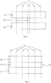
Fig. 1 schematically illustrates a flow chart of a method for making a laser module in the invention; -
Fig. 2 schematically illustrates a schematic diagram of one embodiment in which a substrate is not installed in the invention; -
Fig. 3 schematically illustrates a schematic diagram of another embodiment in which a substrate is not installed in the invention; -
Fig. 4 schematically illustrates a dicing diagram of the embodiment illustrated inFig. 2 ; -
Fig. 5 schematically illustrates a structure diagram of a laser module in which the substrate is installed; -
Fig. 6 schematically illustrates a structure diagram of a laser module in which a metal housing is installed; -
Fig. 7 schematically illustrates a schematic diagram of a laser module array in one embodiment; and -
Fig. 8 schematically illustrates a schematic diagram of a laser module array in another embodiment. - The designators in these figures: 10 first laser module; 11 laser crystal; 12 nonlinear crystal; 13 spacing element; 14 dicing line; 15 substrate; 16 bonding layer; 20 metal holder; 30 array; 40 metal housing.
- The embodiments of the invention will be described in detail below in conjunction with accompanying drawings. But the invention can be implemented in various ways defined by the claims. The invention provides a method for making a laser module. As shown in
Fig. 1 , the making method comprises: - Step 1: Fixing a
laser crystal 11 and anonlinear crystal 12 through at least onespacing element 13 to form a first structure. Specifically, thespacing element 13 may be connected with thelaser crystal 11 and/or thenonlinear crystal 12 through optical bonding or glue bonding. Preferably, thespacing element 13 comprises two parallel bonded surfaces, thelaser crystal 11 and thenonlinear crystal 12 are respectively connected with one of the bonded surfaces so that the input surface and the output surface of thelaser crystal 11 and thenonlinear crystal 12 are parallel to each other and vertical to the direction of a laser beam. - As shown in
Fig. 2 , thelaser crystal 11 and thenonlinear crystal 12 are arranged on the same side of thesubstrate 15, and there is a gap between thelaser crystal 11 and thenonlinear crystal 12. In the embodiment shown inFig. 2 , twoidentical spacing elements 13 are adopted, and thespacing elements 13 are arranged on the two end parts of the strip-shapedlaser crystal 11 andnonlinear crystal 12. In the embodiment shown inFig. 3 , onespacing element 13 is adopted, and thespacing element 13 is located in the middle part of the strip-shapedlaser crystal 11 andnonlinear crystal 12. - In this step, the
laser crystal 11, thenonlinear crystal 12 and thespacing element 13 need to be aligned carefully, so that all surfaces of thelaser crystal 11 and thenonlinear crystal 12 vertical to the laser beam are in a parallel state to form a high quality laser cavity. Preferably, thespacing element 13 can be made from any optical materials easy to be manufactured, such as silicon, silica, or lithium niobate or the like. - As a preferred embodiment, the
laser crystal 11 is doped with Nd3+ ion with doping concentration of 1-3%. Particularly, thelaser crystal 11 is Neodymium doped Yttrium Orthovanadate (Nd:YVO4), Neodymium Doped Gadolinium Orthovanadate (Nd:GdVO4), or Neodymium Doped Yttrium Aluminium Garnet (Nd:YAG). Further, the doping concentration of Nd3+ ion in thelaser crystal 11 is 1%, 2% or 3%. Additionally, the concentration of Nd3+ ion can be determined according to different power (for example the power of green laser), for example, the concentration of Nd3+ ion in thelaser crystal 11 may be 1%, 2% and 3% respectively in the event that the power of the laser module is 100-150mW, 100-500mW and 300-1000mW. - In a preferred embodiment, the
nonlinear crystal 12 is doped with magnesium oxide with molar concentration of 5%. Particularly, thenonlinear crystal 12 is MgO doped Periodically Poled Lithium Niobate (MgO:PPLN), Periodically Poled Lithium Tantalate (PPLT), Periodically Poled Near-stoichiometric Lithium Tantalate (PPSLT), Periodically Poled Potassium Titanyl Phosphate (PPKTP), Potassium Titanyl Phosphate (KTP), Beta Barium Borate (BBO), Bismuth Borate (BIBO) or Lithium Triborate (LBO). - It should be noted that, in the invention, the
laser crystal 11 and thenonlinear crystal 12 of different materials may be combined to obtain different kinds of laser module. Additionally, the concentration of Nd3+ ion in thelaser crystal 11 and the concentration of the magnesium oxide in thenonlinear crystal 12 may also be determined and combined according to the need. Furthermore, the substance doped in thelaser crystal 11 and thenonlinear crystal 12 is not limited to Nd3+ ion and magnesium oxide, also may be other substance commonly used by those skilled in the art. - Step 2: Assembling the first structure on a
substrate 15. Preferably, thesubstrate 15 is made from heat conductive material. Preferably, the heat conductive material may be silicon, sapphire or metal (for example copper, aluminium etc.) or the like. The first structure may be connected with thesubstrate 15 through bonding or welding, also by other ways known in the art. After the first structure is fixed on thesubstrate 15, all the surfaces above-mentioned should be in a parallel state (particularly, the parallelism of each surface of thelaser crystal 11 and thenonlinear crystal 12 is within 10 seconds). - As shown in
Figs. 5-6 , thelaser crystal 11 and thenonlinear crystal 12 are connected with thesubstrate 15 through abonding layer 16. Thebonding layer 16 may be any heat conductive glue or low temperature metal welding layer. For example, the heat conductive glue may be silicon resin, light epoxy resin or silver colloid or the like. When the low temperature metal welding layer is adopted, the surfaces of thelaser crystal 11 and thenonlinear crystal 12 need to be metalized beforehand. - Step 3: Removing at least one
spacing element 13 to form a first laser module. After thespacing element 13 is removed, thelaser crystal 11 and thenonlinear crystal 12 are fixed on thesubstrate 15 so as to form the first laser module. Due to the removal of thespacing element 13, a gap is formed at the position of thespacing element 13, and thelaser crystal 11 and thenonlinear crystal 12 are separated by the gap. - Please refer to
Figs. 3-4 , theStep 3 further comprises: removing at least onespacing element 13 by dicing. At this moment, the strip-shapedlaser crystal 11 andnonlinear crystal 12 are used to manufacture the laser module of the invention. After thelaser crystal 11, thenonlinear crystal 12 and thespacing element 13 are fixed on thesubstrate 15, the part where thespacing element 13 is located may be diced in a dicing manner to form one or more laser modules. - Particularly, in the embodiment shown in
Fig. 6 , thefirst laser module 10 is packaged in ametal housing 40 to improve heat dissipation. Themetal housing 40 may also protect the gap between thelaser crystal 11 and thenonlinear crystal 12. Themetal housing 40 may be made of copper, brass or aluminium or the like. - Step 4: Combining a plurality of
first laser modules 10 into anarray 30, and packaging thenonlinear crystal 12 of eachfirst laser module 10 of the array (30) in a metal holder 20 (Please refer toFig. 7 and Fig. 8 ). In such a way, on one hand, it may be compatible with the transverse polarization direction of a pumping laser diode, on the other hand it may scale up the power. - As shown in
Fig. 7 and Fig. 8 , at least onenonlinear crystal 12 of thefirst laser module 10 may be packaged in themetal holder 20 in order to be compatible with the transverse polarization direction of the pumping laser diode. InFig. 7 and Fig. 8 , thefirst laser module 10 has an optical axis in horizontal direction indicated by arrow, this arrangement may keep compatible with the transverse polarization direction of the laser diode (for example a semiconductor laser of 808nm) for pumping the laser module. - Please refer to
Fig. 8 , thearray 30 is formed by stacking eachfirst laser module 10 in a direction vertical to an optical axis thereof. For example, the centre distance of the pumping laser diode is 500 microns. Correspondingly, the spacing between each laser module inFig. 8 is also 500 microns. By stacking, the green laser with power up to 10W may be generated. - In a preferred embodiment, prior to the
Step 1, the method also comprises the step of preparing thelaser crystal 11, thenonlinear crystal 12 and thespacing element 13. Specifically, the step comprises polishing, coating and cleaning the surfaces of thelaser crystal 11, thenonlinear crystal 12 and thespacing element 13. - Preferably, the input surface of the
laser crystal 11 is coated with high transmission film (preferably, the high transmission film is applied to the laser with a wavelength of 808nm) and high-reflection film (preferably, the high-reflection film is applied to the laser with a wavelength of 1064nm); the output surface of thelaser crystal 11 is coated with anti-reflection film (preferably, the anti-reflection film is applied to the laser with a wavelength of 1064nm) and high-reflection film (preferably, the high-reflection film is applied to the laser with a wavelength of 532nm). Further, the input surface of thenonlinear crystal 12 is coated with anti-reflection film (preferably, the anti-reflection film is applied to the laser with wavelengths of 1064nm and 532nm), the output surface of thenonlinear crystal 12 is coated with high-reflection film (preferably, the high-reflection film is applied to the laser with a wavelength of 1064nm) and an high transmission film (preferably, the high transmission film is applied to the laser with a wavelength of 532nm). - Due to thermal lensing effect, the piano-parallel cavity structure is essentially equivalent to the concave-plano cavity structure. In order to obtain the laser of higher power, it is necessary to optimize the length of the cavity. Therefore, in order to ensure that the laser module in the invention has higher power (e.g., 300-1000mW), it is necessary to optimize the length of the cavity. The length of the cavity of the laser module in the invention may be controlled by the lengths of the
laser crystal 11 and thenonlinear crystal 12, and the length of the gap between thelaser crystal 11 and thenonlinear crystal 12. In a preferred embodiment, the length of thelaser crystal 11 is 0.5-5mm, the length of thenonlinear crystal 12 is 0.5-3mm, the length of the gap is 0.2-8mm, in such a way the length of the cavity is controlled between 1.2mm and 1.6mm. - If the power of the laser module is 100-150mW, then the length of the
laser crystal 11 is 0.5-2mm (particularly, the length may be 0.5mm, 1 mm and 1.5mm), the length of the gap is 0.2-2mm (particularly, the length may be 0.5mm, 1 mm and 1.5mm), and particularly, thelaser crystal 11 may be doped with Nd3+ ion with doping concentration of 3%. - If the power of the laser module is 100-500mW, then the length of the
laser crystal 11 is 1-3mm (particularly, the length may be 1 mm, 2mm and 2.5mm), the length of the gap is 1-3mm (particularly, the length may be 1mm, 2mm and 3mm), and particularly, thelaser crystal 11 may be doped with Nd3+ ion with doping concentration of 2%. - If the power of the laser module is 300-1000mW, then the length of the
laser crystal 11 is 2-3mm (particularly, the length may be 2mm, 2.5mm and 3mm), the length of the gap is 1-5mm (particularly, the length may be 3mm, 4mm and 5mm), and particularly, thelaser crystal 11 may be doped with Nd3+ ion with doping concentration of 1%. - If the power of the laser module is 1000-5000mW, then the length of the
laser crystal 11 is 3-5mm (particularly, the length may be 3mm, 4mm and 5mm), the length of the gap is 5-8mm (particularly, the length may be 6mm, 7mm and 8mm), and particularly, thelaser crystal 11 may be doped with Nd3+ ion with doping concentration of 0.5%. - Particularly, the power of the laser module in all circumstances above-mentioned refers to the range of the highest output power in all circumstances.
Claims (9)
- A method for making a green laser module, wherein the method comprises:Step 1: fixing a laser crystal (11) and a nonlinear crystal (12) through at least one spacing element (13) to form a first structure;Step 2: assembling the first structure on a substrate (15);Step 3: removing the spacing element (13) to form a first laser module;wherein
there is a gap between the laser crystal (11) and the nonlinear crystal (12);
a power of the laser module at a converted frequency which is generated in the nonlinear crystal is between 100mW and 5000mW;
if the power of the laser module at the converted frequency is 100-150mW, then the length of the laser crystal (11) is 0.5-2mm, the laser crystal (11) is doped with Nd3+ ion with doping concentration of 3%, the length of the nonlinear crystal (12) is 0.5-5mm, and the length of the gap is 0.2-2mm;
if the power of the laser module at the converted frequency is 100-500mW, then the length of the laser crystal (11) is 1-3mm, the laser crystal (11) is doped with Nd3+ ion with doping concentration of 2%, the length of the nonlinear crystal (12) is 0.5-5mm, and the length of the gap is 1-3mm;
if the power of the laser module at the converted frequency is 300-1000mW, then the length of the laser crystal (11) is 2-3mm, the laser crystal (11) is doped with Nd3+ ion with doping concentration of 1%, the length of the nonlinear crystal (12) is 0.5-5mm, and the length of the gap is 2-7mm;
if the power of the laser module at the converted frequency is 1000-5000mW, then the length of the laser crystal (11) is 3-5mm, the laser crystal (11) is doped with Nd3+ ion with doping concentration of 0.5%, the length of the nonlinear crystal (12) is 0.5-5mm, and the length of the gap is 3-8mm. - The method according to claim 1, characterized in that, in the Step 1, the spacing element (13) is connected with the laser crystal (11) and/or the nonlinear crystal (12) through glue bonding.
- The method according to claim 1, characterized in that, in the Step 2, the first structure is connected with the substrate (15) through bonding or welding.
- The method according to claim 1, characterized in that the substrate (15) is a heat conductive substrate.
- The method according to claim 1, characterized in that the nonlinear crystal (12) is magnesium oxide doped PPLN, PPLT, PPSLT, PPKTP, KTP, BBO, BIBO or LBO.
- The method according to claim 1, characterized in that the laser crystal (11) is neodymium doped yttrium orthovanadate, neodymium doped gadolinium orthovanadate or neodymium doped yttrium aluminium garnet.
- The method according to any one of claims 1-6, characterized in that the spacing element (13) comprises two parallel bonded surfaces, the laser crystal (11) and the nonlinear crystal (12) are respectively connected with one of the bonded surfaces so that the input surface and the output surface of the laser crystal (11) and the nonlinear crystal (12) are parallel to each other and vertical to the direction of a laser beam.
- The method according to any one of claims 1-7, characterized in that, further comprising Step 4 after the Step 3: combining a plurality of first laser modules into an array (30), and packaging the nonlinear crystal (12) of each first laser module of the array (30) in a metal holder (20).
- The method according to claim 8, characterized in that the array (30) is formed by stacking each first laser module (10) in a direction vertical to an optical axis thereof.
Priority Applications (1)
| Application Number | Priority Date | Filing Date | Title |
|---|---|---|---|
| EP12174305.8A EP2680377B1 (en) | 2012-06-29 | 2012-06-29 | Method for making a laser module |
Applications Claiming Priority (1)
| Application Number | Priority Date | Filing Date | Title |
|---|---|---|---|
| EP12174305.8A EP2680377B1 (en) | 2012-06-29 | 2012-06-29 | Method for making a laser module |
Publications (2)
| Publication Number | Publication Date |
|---|---|
| EP2680377A1 EP2680377A1 (en) | 2014-01-01 |
| EP2680377B1 true EP2680377B1 (en) | 2017-05-10 |
Family
ID=46513644
Family Applications (1)
| Application Number | Title | Priority Date | Filing Date |
|---|---|---|---|
| EP12174305.8A Not-in-force EP2680377B1 (en) | 2012-06-29 | 2012-06-29 | Method for making a laser module |
Country Status (1)
| Country | Link |
|---|---|
| EP (1) | EP2680377B1 (en) |
Family Cites Families (10)
| Publication number | Priority date | Publication date | Assignee | Title |
|---|---|---|---|---|
| US5265116A (en) | 1988-02-02 | 1993-11-23 | Massachusetts Institute Of Technology | Microchip laser |
| SE510442C2 (en) | 1996-09-05 | 1999-05-25 | Fredrik Laurell | microchip Laser |
| US5835518A (en) * | 1997-01-31 | 1998-11-10 | Star Medical Technologies, Inc. | Laser diode array packaging |
| JP4041782B2 (en) * | 2003-09-17 | 2008-01-30 | 昭和オプトロニクス株式会社 | Semiconductor laser pumped solid state laser |
| US20050063441A1 (en) | 2003-09-22 | 2005-03-24 | Brown David C. | High density methods for producing diode-pumped micro lasers |
| US7724797B2 (en) | 2006-04-27 | 2010-05-25 | Spectralus Corporation | Solid-state laser arrays using nonlinear frequency conversion in periodically poled materials |
| US7742510B2 (en) | 2006-04-27 | 2010-06-22 | Spectralus Corporation | Compact solid-state laser with nonlinear frequency conversion using periodically poled materials |
| US7570676B2 (en) | 2006-05-09 | 2009-08-04 | Spectralus Corporation | Compact efficient and robust ultraviolet solid-state laser sources based on nonlinear frequency conversion in periodically poled materials |
| US8068525B2 (en) | 2007-08-30 | 2011-11-29 | Mitsubishi Electric Corporation | Solid-state laser element |
| WO2011140641A1 (en) * | 2010-05-11 | 2011-11-17 | Ye Hu | Packaging method of laser and nonlinear crystal and its application in diode pumped solid state lasers |
-
2012
- 2012-06-29 EP EP12174305.8A patent/EP2680377B1/en not_active Not-in-force
Also Published As
| Publication number | Publication date |
|---|---|
| EP2680377A1 (en) | 2014-01-01 |
Similar Documents
| Publication | Publication Date | Title |
|---|---|---|
| US7742510B2 (en) | Compact solid-state laser with nonlinear frequency conversion using periodically poled materials | |
| US7724797B2 (en) | Solid-state laser arrays using nonlinear frequency conversion in periodically poled materials | |
| EP1763116B1 (en) | Mode control waveguide laser | |
| US20050063441A1 (en) | High density methods for producing diode-pumped micro lasers | |
| CN103996968B (en) | A kind of compound cavity configuration from Raman Yellow light laser | |
| WO2021106757A1 (en) | Laser element, method for manufacturing laser element, laser device, and laser amplification element | |
| CN102570290A (en) | High-power intracavity frequency-doubled semiconductor disk laser | |
| CN103296570A (en) | Single longitudinal mode frequency conversion all-solid-state laser based on non-planar ring cavity structure | |
| CN102893465B (en) | The method for packing of laser crystal and nonlinear crystal and the application in diode pumped solid state thereof | |
| CN102484349B (en) | The method of nonlinear crystal encapsulation and the application in diode pumped solid state thereof | |
| CN104253375B (en) | A kind of high repetition frequency narrow pulse width single-mode green light laser | |
| CN102074889A (en) | A single-frequency visible light laser | |
| US9197027B2 (en) | Method for making laser module | |
| CN103545700A (en) | Integrated single-platform miniature laser | |
| Gan et al. | Compact integrated green laser module for Watt-level display applications | |
| WO2010138116A1 (en) | Compact and efficient visible laser source with high speed modulation | |
| CN106451052A (en) | Apparatus for generating green laser | |
| EP2680377A1 (en) | Method for making laser module | |
| CN102522691A (en) | Neodymium-doped continuous ultraviolet laser adopting linear cavity | |
| CN103022870A (en) | Slat structure based high-power 355nm ultraviolet laser device | |
| CN203503971U (en) | High-power intracavity frequency multiplication semiconductor desk laser | |
| Lecomte et al. | Diode-Pumped Passively Mode-Locked Nd: YVO$_ 4$ Lasers With 40-GHz Repetition Rate | |
| CN107112723B (en) | Array type wavelength convert laser aid | |
| CN203787758U (en) | Compact blue laser chip based on polarized crystal | |
| JP5592444B2 (en) | Laser module manufacturing method |
Legal Events
| Date | Code | Title | Description |
|---|---|---|---|
| PUAI | Public reference made under article 153(3) epc to a published international application that has entered the european phase |
Free format text: ORIGINAL CODE: 0009012 |
|
| 17P | Request for examination filed |
Effective date: 20130614 |
|
| AK | Designated contracting states |
Kind code of ref document: A1 Designated state(s): AL AT BE BG CH CY CZ DE DK EE ES FI FR GB GR HR HU IE IS IT LI LT LU LV MC MK MT NL NO PL PT RO RS SE SI SK SM TR |
|
| AX | Request for extension of the european patent |
Extension state: BA ME |
|
| REG | Reference to a national code |
Ref country code: DE Ref legal event code: R079 Ref document number: 602012032165 Country of ref document: DE Free format text: PREVIOUS MAIN CLASS: H01S0003020000 Ipc: H01S0003109000 |
|
| GRAP | Despatch of communication of intention to grant a patent |
Free format text: ORIGINAL CODE: EPIDOSNIGR1 |
|
| RIC1 | Information provided on ipc code assigned before grant |
Ipc: H01S 3/109 20060101AFI20161102BHEP Ipc: H01S 3/04 20060101ALN20161102BHEP Ipc: H01S 3/042 20060101ALN20161102BHEP Ipc: H01S 3/00 20060101ALN20161102BHEP Ipc: H01S 3/23 20060101ALN20161102BHEP Ipc: H01S 3/16 20060101ALN20161102BHEP Ipc: H01S 3/08 20060101ALN20161102BHEP Ipc: H01S 3/02 20060101ALI20161102BHEP Ipc: H01S 3/0941 20060101ALN20161102BHEP |
|
| INTG | Intention to grant announced |
Effective date: 20161122 |
|
| GRAS | Grant fee paid |
Free format text: ORIGINAL CODE: EPIDOSNIGR3 |
|
| GRAA | (expected) grant |
Free format text: ORIGINAL CODE: 0009210 |
|
| AK | Designated contracting states |
Kind code of ref document: B1 Designated state(s): AL AT BE BG CH CY CZ DE DK EE ES FI FR GB GR HR HU IE IS IT LI LT LU LV MC MK MT NL NO PL PT RO RS SE SI SK SM TR |
|
| REG | Reference to a national code |
Ref country code: GB Ref legal event code: FG4D |
|
| REG | Reference to a national code |
Ref country code: AT Ref legal event code: REF Ref document number: 893236 Country of ref document: AT Kind code of ref document: T Effective date: 20170515 Ref country code: CH Ref legal event code: EP |
|
| REG | Reference to a national code |
Ref country code: IE Ref legal event code: FG4D |
|
| REG | Reference to a national code |
Ref country code: DE Ref legal event code: R096 Ref document number: 602012032165 Country of ref document: DE |
|
| REG | Reference to a national code |
Ref country code: FR Ref legal event code: PLFP Year of fee payment: 6 |
|
| REG | Reference to a national code |
Ref country code: NL Ref legal event code: MP Effective date: 20170510 |
|
| REG | Reference to a national code |
Ref country code: LT Ref legal event code: MG4D |
|
| REG | Reference to a national code |
Ref country code: AT Ref legal event code: MK05 Ref document number: 893236 Country of ref document: AT Kind code of ref document: T Effective date: 20170510 |
|
| PG25 | Lapsed in a contracting state [announced via postgrant information from national office to epo] |
Ref country code: HR Free format text: LAPSE BECAUSE OF FAILURE TO SUBMIT A TRANSLATION OF THE DESCRIPTION OR TO PAY THE FEE WITHIN THE PRESCRIBED TIME-LIMIT Effective date: 20170510 Ref country code: LT Free format text: LAPSE BECAUSE OF FAILURE TO SUBMIT A TRANSLATION OF THE DESCRIPTION OR TO PAY THE FEE WITHIN THE PRESCRIBED TIME-LIMIT Effective date: 20170510 Ref country code: GR Free format text: LAPSE BECAUSE OF FAILURE TO SUBMIT A TRANSLATION OF THE DESCRIPTION OR TO PAY THE FEE WITHIN THE PRESCRIBED TIME-LIMIT Effective date: 20170811 Ref country code: ES Free format text: LAPSE BECAUSE OF FAILURE TO SUBMIT A TRANSLATION OF THE DESCRIPTION OR TO PAY THE FEE WITHIN THE PRESCRIBED TIME-LIMIT Effective date: 20170510 Ref country code: AT Free format text: LAPSE BECAUSE OF FAILURE TO SUBMIT A TRANSLATION OF THE DESCRIPTION OR TO PAY THE FEE WITHIN THE PRESCRIBED TIME-LIMIT Effective date: 20170510 Ref country code: FI Free format text: LAPSE BECAUSE OF FAILURE TO SUBMIT A TRANSLATION OF THE DESCRIPTION OR TO PAY THE FEE WITHIN THE PRESCRIBED TIME-LIMIT Effective date: 20170510 Ref country code: NO Free format text: LAPSE BECAUSE OF FAILURE TO SUBMIT A TRANSLATION OF THE DESCRIPTION OR TO PAY THE FEE WITHIN THE PRESCRIBED TIME-LIMIT Effective date: 20170810 |
|
| PG25 | Lapsed in a contracting state [announced via postgrant information from national office to epo] |
Ref country code: NL Free format text: LAPSE BECAUSE OF FAILURE TO SUBMIT A TRANSLATION OF THE DESCRIPTION OR TO PAY THE FEE WITHIN THE PRESCRIBED TIME-LIMIT Effective date: 20170510 Ref country code: PL Free format text: LAPSE BECAUSE OF FAILURE TO SUBMIT A TRANSLATION OF THE DESCRIPTION OR TO PAY THE FEE WITHIN THE PRESCRIBED TIME-LIMIT Effective date: 20170510 Ref country code: IS Free format text: LAPSE BECAUSE OF FAILURE TO SUBMIT A TRANSLATION OF THE DESCRIPTION OR TO PAY THE FEE WITHIN THE PRESCRIBED TIME-LIMIT Effective date: 20170910 Ref country code: LV Free format text: LAPSE BECAUSE OF FAILURE TO SUBMIT A TRANSLATION OF THE DESCRIPTION OR TO PAY THE FEE WITHIN THE PRESCRIBED TIME-LIMIT Effective date: 20170510 Ref country code: BG Free format text: LAPSE BECAUSE OF FAILURE TO SUBMIT A TRANSLATION OF THE DESCRIPTION OR TO PAY THE FEE WITHIN THE PRESCRIBED TIME-LIMIT Effective date: 20170810 Ref country code: SE Free format text: LAPSE BECAUSE OF FAILURE TO SUBMIT A TRANSLATION OF THE DESCRIPTION OR TO PAY THE FEE WITHIN THE PRESCRIBED TIME-LIMIT Effective date: 20170510 Ref country code: RS Free format text: LAPSE BECAUSE OF FAILURE TO SUBMIT A TRANSLATION OF THE DESCRIPTION OR TO PAY THE FEE WITHIN THE PRESCRIBED TIME-LIMIT Effective date: 20170510 |
|
| PG25 | Lapsed in a contracting state [announced via postgrant information from national office to epo] |
Ref country code: DK Free format text: LAPSE BECAUSE OF FAILURE TO SUBMIT A TRANSLATION OF THE DESCRIPTION OR TO PAY THE FEE WITHIN THE PRESCRIBED TIME-LIMIT Effective date: 20170510 Ref country code: EE Free format text: LAPSE BECAUSE OF FAILURE TO SUBMIT A TRANSLATION OF THE DESCRIPTION OR TO PAY THE FEE WITHIN THE PRESCRIBED TIME-LIMIT Effective date: 20170510 Ref country code: SK Free format text: LAPSE BECAUSE OF FAILURE TO SUBMIT A TRANSLATION OF THE DESCRIPTION OR TO PAY THE FEE WITHIN THE PRESCRIBED TIME-LIMIT Effective date: 20170510 Ref country code: CZ Free format text: LAPSE BECAUSE OF FAILURE TO SUBMIT A TRANSLATION OF THE DESCRIPTION OR TO PAY THE FEE WITHIN THE PRESCRIBED TIME-LIMIT Effective date: 20170510 Ref country code: RO Free format text: LAPSE BECAUSE OF FAILURE TO SUBMIT A TRANSLATION OF THE DESCRIPTION OR TO PAY THE FEE WITHIN THE PRESCRIBED TIME-LIMIT Effective date: 20170510 |
|
| REG | Reference to a national code |
Ref country code: CH Ref legal event code: PL |
|
| REG | Reference to a national code |
Ref country code: DE Ref legal event code: R097 Ref document number: 602012032165 Country of ref document: DE |
|
| PG25 | Lapsed in a contracting state [announced via postgrant information from national office to epo] |
Ref country code: IT Free format text: LAPSE BECAUSE OF FAILURE TO SUBMIT A TRANSLATION OF THE DESCRIPTION OR TO PAY THE FEE WITHIN THE PRESCRIBED TIME-LIMIT Effective date: 20170510 Ref country code: SM Free format text: LAPSE BECAUSE OF FAILURE TO SUBMIT A TRANSLATION OF THE DESCRIPTION OR TO PAY THE FEE WITHIN THE PRESCRIBED TIME-LIMIT Effective date: 20170510 |
|
| PLBE | No opposition filed within time limit |
Free format text: ORIGINAL CODE: 0009261 |
|
| STAA | Information on the status of an ep patent application or granted ep patent |
Free format text: STATUS: NO OPPOSITION FILED WITHIN TIME LIMIT |
|
| REG | Reference to a national code |
Ref country code: IE Ref legal event code: MM4A |
|
| 26N | No opposition filed |
Effective date: 20180213 |
|
| PG25 | Lapsed in a contracting state [announced via postgrant information from national office to epo] |
Ref country code: LI Free format text: LAPSE BECAUSE OF NON-PAYMENT OF DUE FEES Effective date: 20170630 Ref country code: IE Free format text: LAPSE BECAUSE OF NON-PAYMENT OF DUE FEES Effective date: 20170629 Ref country code: CH Free format text: LAPSE BECAUSE OF NON-PAYMENT OF DUE FEES Effective date: 20170630 Ref country code: LU Free format text: LAPSE BECAUSE OF NON-PAYMENT OF DUE FEES Effective date: 20170629 |
|
| PG25 | Lapsed in a contracting state [announced via postgrant information from national office to epo] |
Ref country code: SI Free format text: LAPSE BECAUSE OF FAILURE TO SUBMIT A TRANSLATION OF THE DESCRIPTION OR TO PAY THE FEE WITHIN THE PRESCRIBED TIME-LIMIT Effective date: 20170510 |
|
| REG | Reference to a national code |
Ref country code: BE Ref legal event code: MM Effective date: 20170630 |
|
| REG | Reference to a national code |
Ref country code: FR Ref legal event code: PLFP Year of fee payment: 7 |
|
| PG25 | Lapsed in a contracting state [announced via postgrant information from national office to epo] |
Ref country code: BE Free format text: LAPSE BECAUSE OF NON-PAYMENT OF DUE FEES Effective date: 20170630 |
|
| PG25 | Lapsed in a contracting state [announced via postgrant information from national office to epo] |
Ref country code: MT Free format text: LAPSE BECAUSE OF NON-PAYMENT OF DUE FEES Effective date: 20170629 |
|
| PG25 | Lapsed in a contracting state [announced via postgrant information from national office to epo] |
Ref country code: HU Free format text: LAPSE BECAUSE OF FAILURE TO SUBMIT A TRANSLATION OF THE DESCRIPTION OR TO PAY THE FEE WITHIN THE PRESCRIBED TIME-LIMIT; INVALID AB INITIO Effective date: 20120629 Ref country code: MC Free format text: LAPSE BECAUSE OF FAILURE TO SUBMIT A TRANSLATION OF THE DESCRIPTION OR TO PAY THE FEE WITHIN THE PRESCRIBED TIME-LIMIT Effective date: 20170510 |
|
| PG25 | Lapsed in a contracting state [announced via postgrant information from national office to epo] |
Ref country code: CY Free format text: LAPSE BECAUSE OF NON-PAYMENT OF DUE FEES Effective date: 20170510 |
|
| PG25 | Lapsed in a contracting state [announced via postgrant information from national office to epo] |
Ref country code: MK Free format text: LAPSE BECAUSE OF FAILURE TO SUBMIT A TRANSLATION OF THE DESCRIPTION OR TO PAY THE FEE WITHIN THE PRESCRIBED TIME-LIMIT Effective date: 20170510 |
|
| PG25 | Lapsed in a contracting state [announced via postgrant information from national office to epo] |
Ref country code: TR Free format text: LAPSE BECAUSE OF FAILURE TO SUBMIT A TRANSLATION OF THE DESCRIPTION OR TO PAY THE FEE WITHIN THE PRESCRIBED TIME-LIMIT Effective date: 20170510 |
|
| PG25 | Lapsed in a contracting state [announced via postgrant information from national office to epo] |
Ref country code: PT Free format text: LAPSE BECAUSE OF FAILURE TO SUBMIT A TRANSLATION OF THE DESCRIPTION OR TO PAY THE FEE WITHIN THE PRESCRIBED TIME-LIMIT Effective date: 20170510 |
|
| PG25 | Lapsed in a contracting state [announced via postgrant information from national office to epo] |
Ref country code: AL Free format text: LAPSE BECAUSE OF FAILURE TO SUBMIT A TRANSLATION OF THE DESCRIPTION OR TO PAY THE FEE WITHIN THE PRESCRIBED TIME-LIMIT Effective date: 20170510 |
|
| PGFP | Annual fee paid to national office [announced via postgrant information from national office to epo] |
Ref country code: FR Payment date: 20200611 Year of fee payment: 9 Ref country code: DE Payment date: 20200617 Year of fee payment: 9 |
|
| PGFP | Annual fee paid to national office [announced via postgrant information from national office to epo] |
Ref country code: GB Payment date: 20200617 Year of fee payment: 9 |
|
| REG | Reference to a national code |
Ref country code: DE Ref legal event code: R119 Ref document number: 602012032165 Country of ref document: DE |
|
| GBPC | Gb: european patent ceased through non-payment of renewal fee |
Effective date: 20210629 |
|
| PG25 | Lapsed in a contracting state [announced via postgrant information from national office to epo] |
Ref country code: GB Free format text: LAPSE BECAUSE OF NON-PAYMENT OF DUE FEES Effective date: 20210629 Ref country code: DE Free format text: LAPSE BECAUSE OF NON-PAYMENT OF DUE FEES Effective date: 20220101 |
|
| PG25 | Lapsed in a contracting state [announced via postgrant information from national office to epo] |
Ref country code: FR Free format text: LAPSE BECAUSE OF NON-PAYMENT OF DUE FEES Effective date: 20210630 |