EP2677522A1 - Method and system for fast initialization of a memory unit - Google Patents
Method and system for fast initialization of a memory unit Download PDFInfo
- Publication number
- EP2677522A1 EP2677522A1 EP13172059.1A EP13172059A EP2677522A1 EP 2677522 A1 EP2677522 A1 EP 2677522A1 EP 13172059 A EP13172059 A EP 13172059A EP 2677522 A1 EP2677522 A1 EP 2677522A1
- Authority
- EP
- European Patent Office
- Prior art keywords
- memory unit
- data
- registers
- power
- initialization
- Prior art date
- Legal status (The legal status is an assumption and is not a legal conclusion. Google has not performed a legal analysis and makes no representation as to the accuracy of the status listed.)
- Granted
Links
Images



Classifications
-
- G—PHYSICS
- G11—INFORMATION STORAGE
- G11C—STATIC STORES
- G11C7/00—Arrangements for writing information into, or reading information out from, a digital store
- G11C7/20—Memory cell initialisation circuits, e.g. when powering up or down, memory clear, latent image memory
-
- G—PHYSICS
- G11—INFORMATION STORAGE
- G11C—STATIC STORES
- G11C16/00—Erasable programmable read-only memories
- G11C16/02—Erasable programmable read-only memories electrically programmable
- G11C16/06—Auxiliary circuits, e.g. for writing into memory
- G11C16/10—Programming or data input circuits
- G11C16/20—Initialising; Data preset; Chip identification
-
- G—PHYSICS
- G06—COMPUTING OR CALCULATING; COUNTING
- G06F—ELECTRIC DIGITAL DATA PROCESSING
- G06F1/00—Details not covered by groups G06F3/00 - G06F13/00 and G06F21/00
- G06F1/26—Power supply means, e.g. regulation thereof
- G06F1/32—Means for saving power
- G06F1/3203—Power management, i.e. event-based initiation of a power-saving mode
- G06F1/3234—Power saving characterised by the action undertaken
- G06F1/325—Power saving in peripheral device
- G06F1/3275—Power saving in memory, e.g. RAM, cache
-
- G—PHYSICS
- G06—COMPUTING OR CALCULATING; COUNTING
- G06F—ELECTRIC DIGITAL DATA PROCESSING
- G06F11/00—Error detection; Error correction; Monitoring
- G06F11/07—Responding to the occurrence of a fault, e.g. fault tolerance
- G06F11/14—Error detection or correction of the data by redundancy in operations
- G06F11/1402—Saving, restoring, recovering or retrying
-
- G—PHYSICS
- G06—COMPUTING OR CALCULATING; COUNTING
- G06F—ELECTRIC DIGITAL DATA PROCESSING
- G06F12/00—Accessing, addressing or allocating within memory systems or architectures
- G06F12/02—Addressing or allocation; Relocation
- G06F12/06—Addressing a physical block of locations, e.g. base addressing, module addressing, memory dedication
- G06F12/0646—Configuration or reconfiguration
-
- G—PHYSICS
- G06—COMPUTING OR CALCULATING; COUNTING
- G06F—ELECTRIC DIGITAL DATA PROCESSING
- G06F15/00—Digital computers in general; Data processing equipment in general
- G06F15/16—Combinations of two or more digital computers each having at least an arithmetic unit, a program unit and a register, e.g. for a simultaneous processing of several programs
- G06F15/177—Initialisation or configuration control
-
- G—PHYSICS
- G06—COMPUTING OR CALCULATING; COUNTING
- G06F—ELECTRIC DIGITAL DATA PROCESSING
- G06F3/00—Input arrangements for transferring data to be processed into a form capable of being handled by the computer; Output arrangements for transferring data from processing unit to output unit, e.g. interface arrangements
- G06F3/06—Digital input from, or digital output to, record carriers, e.g. RAID, emulated record carriers or networked record carriers
- G06F3/0601—Interfaces specially adapted for storage systems
- G06F3/0628—Interfaces specially adapted for storage systems making use of a particular technique
- G06F3/0629—Configuration or reconfiguration of storage systems
- G06F3/0632—Configuration or reconfiguration of storage systems by initialisation or re-initialisation of storage systems
-
- G—PHYSICS
- G06—COMPUTING OR CALCULATING; COUNTING
- G06F—ELECTRIC DIGITAL DATA PROCESSING
- G06F3/00—Input arrangements for transferring data to be processed into a form capable of being handled by the computer; Output arrangements for transferring data from processing unit to output unit, e.g. interface arrangements
- G06F3/06—Digital input from, or digital output to, record carriers, e.g. RAID, emulated record carriers or networked record carriers
- G06F3/0601—Interfaces specially adapted for storage systems
- G06F3/0628—Interfaces specially adapted for storage systems making use of a particular technique
- G06F3/0646—Horizontal data movement in storage systems, i.e. moving data in between storage devices or systems
- G06F3/065—Replication mechanisms
Definitions
- Integrated circuit (IC) devices can be fabricated to include a microprocessor and embedded memory.
- embedded flash memory is fabricated on a substrate along with a microprocessor unit and other supporting circuitry to produce a monolithic microcontroller or system-on-a-chip (SOC).
- SOC system-on-a-chip
- the memory unit has a non-volatile memory array and processing logic and the non-volatile memory array stores initialization data that is used by the processing logic to perform input/output operations of the memory unit.
- the method involves storing the initialization data in retention registers within the memory unit, wherein the retention registers are separate from the non-volatile memory array and retain data while the memory unit is power gated, using the stored initialization data in the retention registers to initialize the memory unit upon exiting the power gating.
- a memory unit includes a non-volatile memory array, processing logic, retention registers, and a controller.
- the non-volatile memory array stores initialization data and the processing logic is configured to perform input/output operations of the memory unit.
- the processing logic includes volatile registers for storing the initialization data when the memory unit is in a normal operating mode.
- the retention registers are configured to store data even when the memory unit is power gated from a power source.
- the controller is configured to store the initialization data in the retention registers and to populate the volatile registers of the processing logic using the initialization data from the retention registers upon transition from a low power mode to the normal operating mode.
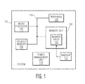
- Fig. 1 depicts an embodiment of a computer system 100 that includes a microprocessor 102, volatile memory 104, a peripheral 106, a memory unit 108, a power management unit 110, and a band gap 112.
- the microprocessor, the volatile memory, the peripheral, and the memory unit are connected by a system bus 114 that serves as a data pathway to exchange digital data.
- the computer system is a microcontroller for use in applications such as e-metering, hearing aids, wireless sensor networks, or mobile devices. Other uses of the computer system are possible.
- the microprocessor 102 is a micro instruction processor, also referred to as a central processing unit (CPU), as is known in the field and the volatile memory 104 is a memory system such as random access memory (RAM) that provides volatile memory for the computer system 100, e.g., memory that does not retain its stored data upon power down.
- the microprocessor executes instructions that are stored in the memory unit 108.
- the peripheral 106 may include a device such as an analog signal processor, a touch screen controller, an I/O port, a speaker, or any other logic circuit that processes digital data communicated via the system bus. Although a single peripheral is depicted in Fig. 1 , the computer system may include more than one peripheral.
- the memory unit is a non-volatile memory system that includes a memory array 116 to provide non-volatile memory to the computer system, e.g., memory such as flash memory that retains its stored data upon power down.
- memory such as flash memory that retains its stored data upon power down.
- the memory unit does include some volatile registers in the processing circuitry that support data I/O operations.
- the power management unit 110 manages the distribution of electrical power to the microprocessor, the volatile memory, the peripheral, and the memory unit. In a working system, the power unit is connected to a power source such as a battery.
- the bandgap is an element that provides a reference signal, e.g., a reference voltage and/or reference current to the memory unit.
- a bandgap circuit may be internal to the memory unit.
- bandgap circuits are external to the memory unit and a reference signal is provided to the memory unit through an analog pin.
- all of the elements of the computer system 100 of Fig. 1 are fabricated on a single substrate, e.g., on a single silicon semiconductor substrate.
- IC devices with such a combination of functional units are often referred to as SOC devices.
- each functional unit is often referred to as an intellectual property (IP) block and the memory unit 108 is often referred to as "embedded" memory.
- IP intellectual property
- one or more of the functional units may be fabricated on a separate substrate and packaged together with the other functional units as a single packaged IC component. For example, multiple IC dies may be packaged into a multi-die package as is known in the field.
- a computer system such as the computer system 100 depicted in Fig. 1 is often part of a battery operated electronic device such as a smart phone, a pad computer, a remote sensor, or various other wireless devices.
- a battery operated electronic device such as a smart phone, a pad computer, a remote sensor, or various other wireless devices.
- power conservation is a high priority and various techniques have been implemented to conserve power.
- One known technique for conserving power is "power gating.” Power gating involves using a power switch to gate off a particular IP block from the power source, e.g., to cut off the transmission of electrical power from the battery.
- the memory unit 108 (or a portion of the memory unit) can be power gated during times when the computer system is in a standby or a low-power mode.
- Power gating of the memory unit prevents power loss from voltage or current leakage at the memory unit and therefore enhances power conservation.
- power gating the memory unit typically causes the registers of the I/O processing logic to lose their stored data.
- any trimming, redundancy, and/or security data held in registers of the memory unit's processing logic is lost when the memory unit is power gated.
- the power gate is opened (e.g., a power switch is closed) to allow power to flow back to the power gated IP block.
- the initialization data When the computer system 100 returns to a normal operating mode and the memory unit 108 is no longer power gated, the initialization data must be read from the memory array 116 and reloaded into the registers of the I/O processing circuitry before I/O operations between the memory unit and the microprocessor 102 can begin. Reading the initialization data from the memory array is a time-consuming process that adds to the time required to wake up the computer system, e.g., to transition the computer system from a low-power mode to a normal operating mode.
- the memory unit 108 is fabricated to include retention registers that are separate from the memory array and that can store the initialization data even when the memory unit is power gated.
- the retention registers store the trimming data, redundancy data, and/or security data that is used to initialize the memory unit.
- the initialization data used to populate the I/O processing logic is read from the retention registers instead of from the memory array, which as is explained below, is a much faster operation, resulting in a faster initialization of the memory unit and a faster overall wake up time for the computer system.
- Fig. 2 depicts an expanded view of the memory unit 108 of Fig. 1 in which the memory unit is configured to support rapid transition from a low-power mode to a normal operating mode.
- the memory unit includes the memory array 116 and a memory unit controller 118.
- the memory array is an array of memory cells such as flash memory cells or electrically erasable programmable read only memory (EEPROM) cells.
- EEPROM electrically erasable programmable read only memory
- the memory array stores initialization data 120 that is used by the memory unit controller to support the reading of data from the memory array and the writing of data to the memory array.
- the initialization data is stored in an index row or index sector of the memory array and includes trimming data, redundancy data, and security data.
- the memory unit also includes I/O processing logic 132 that is configured to support read operations from the memory array 116 and write operations to the memory array and may include, for example, word line repair logic, bit line repair logic, word decoders, bit decoders, and access control logic.
- the I/O processing logic also includes volatile registers 138, which store the initialization data for use during I/O processing.
- the redundancy data specifies repair addresses that are used to identify defective memory cells. For example, the redundancy data remaps defective memory cells to other specified memory cells, often referred to as "redundant" cells.
- the memory array 116 and I/O processing logic 132 are often pre-designed by an outside vendor and provided to an SOC device designer as an IP block.
- a memory IP block that includes the memory array 116 and the I/O processing logic 132 is indicated by dashed line box 140.
- retention registers which are typically outside of the memory IP block, are used to enable fast memory unit initialization.
- the initialization logic can be a combination of hardware, software, and/or firmware that is configured to manage the storing of initialization data in the retention registers and the populating of the volatile registers 138 of the I/O processing logic 132 upon transition of the memory unit from a low-power mode to a normal operating mode.
- only the memory IP block 140 of the memory unit is power gated.
- power gating the memory unit 108 involves power gating only the memory IP block 140.
- the memory unit controller 118 of the memory unit is also power gated.
- the retention registers 134 may have an external power source that is not power gated or the retention registers may be configured as non-volatile memory registers, e.g., state retention flip-flops. In still another embodiment, it is possible that the state retention registers could be implemented within the memory IP block 140.
- the power switch 130 functions as a digital switch that connects the power management unit 110 to the memory unit 108 in a normal operating mode and disconnects or "gates" the power management unit from the memory unit in a low-power mode.
- the computer system 100 performs the primary functions for which the computer system was designed, e.g., microcontroller functions, and in a low power mode, the computer system performs a limited set of operations, such as a low power sensing operation or the computer system simply waits for an input signal that triggers a wake up.
- the power switch controls power to the memory IP block 140, that is, the memory IP block can be power gated.
- the power switch is typically controlled by an input from the power management unit but can be controlled by an input from a different functional unit such as the microprocessor 102.
- the power switch is implemented as a PMOS transistor or as an NMOS transistor, although other embodiments of the power switch are possible.
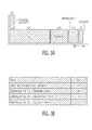
- Fig. 3A depicts a sequence of specific initialization steps that are implemented before a memory unit is fully operational, e.g., ready for data to be read from the memory unit or written to the memory unit.
- a reset pulse is applied to the processing circuitry in the memory IP block 140 to ensure that all of the internal circuits are completely discharged.
- the reset pulse takes approximately 60% of the entire time required to complete the memory unit wakeup process.
- internal voltages In parallel with the reset pulse, in a step identified as "internal voltages", internal voltages of elements of the I/O processing logic are allowed to stabilize. As shown in Fig. 3A , this process takes approximately 6% of the entire time required to complete the memory unit initialization process and is done in parallel with the internal voltage stabilization.
- trimming data is read from the memory array and then populated into the appropriate volatile registers of the I/O processing logic.
- the initialization operation related to setting the trimming data takes approximately 24% of the entire time required to complete the memory unit initialization process.
- redundancy data is read from the memory array and then populated into the appropriate volatile registers of the I/O processing logic.
- the initialization operation related to setting the redundancy data takes approximately 11% of the entire time required to complete the memory unit initialization process. Without taking security precautions into account, data can be read from the memory unit once the trimming and redundancy initialization operations are completed.
- a next step (identified as "security"), security data is read from the memory array and then populated into the appropriate volatile registers of the I/O processing logic.
- the initialization operation related to setting the security data takes approximately 5% of the entire time required to complete the memory unit initialization process.
- Fig. 3B is a summary of the time required for each step of the initialization process relative to the entire time required to complete the memory unit initialization process.
- the retention registers 134 are used to store trimming data and the stored trimming data is used to populate the volatile registers 138 of the I/O processing logic 132 when the computer system 100 is requested to transition from a low power mode to a normal operating mode.
- the trimming data is read from the retention registers instead of from the memory array 116, only a very short pulse reset is required and the time required to read the initialization data is greatly reduced.
- the trimming, redundancy, and security initialization operations all require initialization data to be read from the memory array. The balance between storing initialization data in the retention registers and the corresponding reduction in the initialization time is described below with reference to Figs. 4A - 5B .
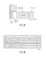
- Figs. 4A and 4B illustrate a timeline of a memory unit initialization process in which trimming data is stored in the retention registers 134 for use during the memory unit initialization process.
- the time required for the reset pulse can be reduced to approximately 0.6% of the entire initialization time and the operation related to setting the trimming data can be reduced to approximately 0.9% of the entire initialization time.
- the internal voltages of the I/O processing logic 132 still have to be stabilized but this can be done in parallel with the reset pulse and the setting of the trimming data.
- the time required for voltage stabilization is the controlling time period and the initialization operation related to setting the redundancy data does not start until after the internal voltages are stabilized. Because only the trimming data is stored in the retention registers, in subsequent steps, the redundancy data and the security data must be read from the memory array 116 and populated in the registers of the I/O processing logic as described above with reference to Fig. 3A . With the substantial reductions in the time required for pulse reset and the time required to set the trimming data, the total initialization time of the process described with reference to Fig. 4A is approximately 22% of the entire time required for a conventional initialization process as described with reference to Fig. 3A .
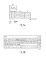
- both the trimming data and the redundancy data are stored in the retention registers 134 and used to transition the computer system 100 from a low power mode to a normal operating mode.
- the time required for the reset and trimming operations is reduced to approximately 0.6% and 0.9%, respectively, of the entire time of the conventional initialization process described with reference to Fig. 3A .
- Reading the redundancy data from the retention registers reduces the time required for the redundancy initialization operation to approximately 9.5% of the total time required.
- a significant benefit of storing both the trimming and redundancy data in the retention registers is that the initialization operation related to the redundancy data can proceed in parallel with the stabilization of the internal voltages.
- Implementing the operations related to the trimming data and the redundancy data in parallel with the stabilization of the internal voltages is illustrated in the timeline of Fig. 5A .
- the total time for the initialization process is reduced to approximately 16% of the entire time required for a conventional initialization process as described with reference to Fig. 3A .
- read operations can commence once the volatile registers of the processing logic are populated with the redundancy data.
- the initialization data In order for the initialization data to be read from the retention registers 134, the initialization data must first be read from the memory array 116 and written to the retention registers. In an embodiment, reading the initialization data from the memory array and writing the initialization data to the retention registers occurs during a first initialization operation, for example, when the computer system transitions from an off state to an on state, often referred to as a "cold start.” In an embodiment, a cold start occurs when the computer system transitions from an off state to a normal operating mode and a warm start occurs when the computer system transitions from a low-power or standby mode to a normal operating mode. In an embodiment, a warm start occurs after the memory unit 108 has been power gated.
- the warm start occurs upon exiting the power gating, for example, when the power switch is closed so that electrical power is provided to the memory unit from a power source such as a battery.
- the initialization data is read from the memory array and programmed into the volatile registers 138 of the I/O processing logic 132.
- the desired portion of the read initialization data is also stored in the retention registers 134.
- some portion of the initialization data, which has previously been stored in the retention registers is read from the retention registers instead of from the memory array.
- Fig. 6 is a process flow diagram of a conventional initialization operation as described above with reference to Fig. 3A .
- a reset operation is performed, e.g., a reset pulse is applied.
- the trimming data is read from the memory array and at block 204, the trimming data is programmed into the volatile registers of the I/O processing logic.
- the redundancy data is read from the memory array and at block 208, the redundancy data is programmed into the volatile registers of the I/O processing logic.
- the security data is read from the memory array and at block 212, the security data is programmed into the volatile registers of the I/O processing logic, which ends the initialization process.
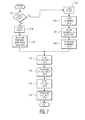
- Fig. 7 is a process flow diagram of an initialization operation that utilizes retention registers to store trimming data as is described above with reference to Figs. 4A and 4B .
- this is the first initialization process. For example, is the initialization process part of a cold start or a warm start. If the initialization process is part of a cold start (such that no initialization data is stored in the retention registers), at block 220A, a long reset operation is performed and at block 224, trimming data is read from the memory array. At block 226, the trimming data is stored in the retention registers 134 for use in a subsequent initialization process.
- the trimming data is programmed into the volatile registers 138 of the I/O processing logic 132. If the initialization process is part of a warm start that involves removing a power gate (such that the trimming data was previously stored in the retention registers), then at block 220B, a short reset pulse operation is performed and at block 230, the trimming data is read from the retention registers instead of from the memory array and used to populate the volatile registers of the I/O processing logic. Once the volatile registers of the I/O processing logic have been populated with the trimming data, at block 232, redundancy data is read from the memory array and at block 234, the redundancy data is programmed into the volatile registers of the I/O processing logic.
- the security data is read from the memory array and at block 238, security data is programmed into the volatile registers of the I/O processing logic, which ends the initialization process.
- the time savings of this initialization process is described with reference to Figs. 4A and 4B .
- Fig. 8 is a process flow diagram of an initialization operation that utilizes retention registers to store trimming data along with redundancy data as is described above with reference to Figs. 5A and 5B .
- this is the first initialization process. For example, is the initialization process part of a cold start or a warm start. If the initialization process is part of a cold start, at block 242A, a long reset operation is performed and at block 244, trimming data is read from the memory array. At block 246, the trimming data is stored in the retention registers 134 for use in a subsequent initialization process.
- the trimming data is programmed into the volatile registers 138 of the I/O processing logic 132. Additionally, if the initialization process is part of a cold start, at block 250, redundancy data is read from the memory array and at block 252, the redundancy data is stored in the retention registers for use in a subsequent initialization process. At block 254, the redundancy data is programmed into the volatile registers of the I/O processing logic.
- the initialization process is part of a warm start that involves opening the power gate (such that the trimming and redundancy data have previously been stored in the retention registers)
- a short reset operation is performed and at block 256, the trimming data is read from the retention registers instead of from the memory array and the trimming data in the retention registers is used to populate the volatile registers of the I/O processing logic and, at block 258, redundancy data is read from the retention registers instead of from the memory array and the redundancy data in the retention registers is used to populate the volatile registers of the I/O processing logic.
- retention registers 134 are added to the controller 118 of the memory unit 108 to enable fast memory unit initialization.
- the number of retention registers required depends on the amount of data that is to be stored and each retention register requires a certain amount if physical space on the IC device.
- the additional area for a typical flash controller IP is based on the area required for the retention registers.
- An example of the area required for retention registers (as a percentage of the total available area on the controller) is provided below in Table 1.
- Table 1 Flash controller IP property Number of nd2 equivalent cells Area overhead for retention option Trimming data Trimming and redundancy data 128 bit bus 28k 0.4% 8.1% 256 bit bus 42k 0.3% 5.4%
- the physical area required for the retention registers is a very small percentage of the overall area of the IC device.
- Table 2 provides a summary comparison of how wake up times (as a percentage of the total wake up time using a conventional initialization process) are affected when utilizing retention registers for trimming data or trimming data and redundancy data relative to no retention registers. Table 2 also indicates the area overhead required for each scenario.
- the memory unit has a non-volatile memory array and processing logic and the non-volatile memory array stores initialization data that is used by the processing logic to perform input/output operations of the memory unit.
- the memory unit is powered up.
- initialization data is read from the non-volatile memory array.
- the initialization data is stored in retention registers of the memory unit.
- volatile registers of the processing logic are populated with the initialization data.
- the memory unit is power gated such that the initialization data is no longer stored in the volatile registers of the processing logic.
- the memory unit is powered up after the power gating.
- the memory unit is initialized using the initialization data that is stored in the retention registers.
- the computer-useable or computer-readable storage medium can be an electronic, magnetic, optical, electromagnetic, infrared, or semiconductor system (or apparatus or device).
- Examples of a computer-useable and computer-readable storage media include a semiconductor or solid state memory, magnetic tape, a removable computer diskette, a random access memory (RAM), a read-only memory (ROM), a rigid magnetic disk, and an optical disk.
- Current examples of optical disks include a compact disk with read only memory (CD-ROM), a compact disk with read/write (CD-R/W), and a digital video disk (DVD).
- embodiments of the invention may be implemented entirely in hardware or in an implementation containing both hardware and software elements.
- the software may include but is not limited to firmware, resident software, microcode, etc.
Landscapes
- Techniques For Improving Reliability Of Storages (AREA)
Abstract
Description
- Integrated circuit (IC) devices can be fabricated to include a microprocessor and embedded memory. For example, embedded flash memory is fabricated on a substrate along with a microprocessor unit and other supporting circuitry to produce a monolithic microcontroller or system-on-a-chip (SOC). These microcontrollers and SOC devices are often used in battery-powered electronic devices in which power conservation is vitally important.
- One technique for conserving power in such IC devices is to "power gate" the embedded flash memory during a low-power or standby mode. Although power gating works well to conserve power, power gating causes internal input/output (I/O) processing settings of the embedded flash memory, such as trimming, redundancy, and security settings, to be lost when the power is gated. Upon wakeup of the embedded flash memory, initialization data must be repopulated within the I/O circuitry to initialize the embedded flash memory. Until the embedded flash memory is initialized, data stored in the memory is not available for use by the microprocessor.
- Embodiments of a method for operating a computer system are disclosed. In one embodiment, the memory unit has a non-volatile memory array and processing logic and the non-volatile memory array stores initialization data that is used by the processing logic to perform input/output operations of the memory unit. The method involves storing the initialization data in retention registers within the memory unit, wherein the retention registers are separate from the non-volatile memory array and retain data while the memory unit is power gated, using the stored initialization data in the retention registers to initialize the memory unit upon exiting the power gating.
- Embodiments of a memory unit are also disclosed. In one embodiment, a memory unit includes a non-volatile memory array, processing logic, retention registers, and a controller. The non-volatile memory array stores initialization data and the processing logic is configured to perform input/output operations of the memory unit. The processing logic includes volatile registers for storing the initialization data when the memory unit is in a normal operating mode. The retention registers are configured to store data even when the memory unit is power gated from a power source. The controller is configured to store the initialization data in the retention registers and to populate the volatile registers of the processing logic using the initialization data from the retention registers upon transition from a low power mode to the normal operating mode.
- Other aspects and advantages of embodiments in accordance with the invention will become apparent from the following detailed description, taken in conjunction with the accompanying drawings, illustrated by way of example of the principles of the invention.
-
Fig. 1 depicts an embodiment of a computer system that includes a microprocessor, volatile memory, a peripheral, a memory unit, a power management unit, and a band gap. -
Fig. 2 depicts an expanded view of the memory unit ofFig. 1 in which the memory unit is configured to support rapid transition from a low-power mode to a normal operating mode. -
Figs. 3A and 3B illustrate a timeline of a conventional memory unit initialization process. -
Figs. 4A and 4B illustrate a timeline of a memory unit initialization process in which trimming data is stored in retention registers for use during the memory unit initialization process. -
Figs. 5A and 5B illustrate a timeline of a memory unit initialization process in which both trimming data and redundancy data are stored in retention registers for use during the memory unit initialization process. -
Fig. 6 is a process flow diagram of a conventional initialization operation as described above with reference toFigs. 3A and 3B . -
Fig. 7 is a process flow diagram of an initialization operation that utilizes retention registers to store trimming data as is described above with reference toFigs. 4A and 4B . -
Fig. 8 is a process flow diagram of an initialization operation that utilizes retention registers to store trimming data along with redundancy data as is described above with reference toFigs. 5A and 5B . -
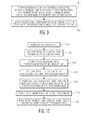
Fig. 9 is a process flow diagram of an embodiment of a method for operating a memory unit of a computer system. -
Fig. 10 is a process flow diagram of an embodiment of a method for operating a memory unit of a computer system. - Throughout the description, similar reference numbers may be used to identify similar elements.
- It will be readily understood that the components of the embodiments as generally described herein and illustrated in the appended figures could be arranged and designed in a wide variety of different configurations. Thus, the following more detailed description of various embodiments, as represented in the figures, is not intended to limit the scope of the present disclosure, but is merely representative of various embodiments. While the various aspects of the embodiments are presented in drawings, the drawings are not necessarily drawn to scale unless specifically indicated.
- The present invention may be embodied in other specific forms without departing from its spirit or essential characteristics. The described embodiments are to be considered in all respects only as illustrative and not restrictive. The scope of the invention is, therefore, indicated by the appended claims rather than by this detailed description. All changes which come within the meaning and range of equivalency of the claims are to be embraced within their scope.
- Reference throughout this specification to features, advantages, or similar language does not imply that all of the features and advantages that may be realized with the present invention should be or are in any single embodiment of the invention. Rather, language referring to the features and advantages is understood to mean that a specific feature, advantage, or characteristic described in connection with an embodiment is included in at least one embodiment of the present invention. Thus, discussions of the features and advantages, and similar language, throughout this specification may, but do not necessarily, refer to the same embodiment.
- Furthermore, the described features, advantages, and characteristics of the invention may be combined in any suitable manner in one or more embodiments. One skilled in the relevant art will recognize, in light of the description herein, that the invention can be practiced without one or more of the specific features or advantages of a particular embodiment. In other instances, additional features and advantages may be recognized in certain embodiments that may not be present in all embodiments of the invention.
- Reference throughout this specification to "one embodiment," "an embodiment," or similar language means that a particular feature, structure, or characteristic described in connection with the indicated embodiment is included in at least one embodiment of the present invention. Thus, the phrases "in one embodiment," "in an embodiment," and similar language throughout this specification may, but do not necessarily, all refer to the same embodiment.
-
Fig. 1 depicts an embodiment of acomputer system 100 that includes amicroprocessor 102,volatile memory 104, a peripheral 106, amemory unit 108, apower management unit 110, and aband gap 112. As illustrated inFig. 1 , the microprocessor, the volatile memory, the peripheral, and the memory unit are connected by asystem bus 114 that serves as a data pathway to exchange digital data. In an embodiment, the computer system is a microcontroller for use in applications such as e-metering, hearing aids, wireless sensor networks, or mobile devices. Other uses of the computer system are possible. - In an embodiment, the
microprocessor 102 is a micro instruction processor, also referred to as a central processing unit (CPU), as is known in the field and thevolatile memory 104 is a memory system such as random access memory (RAM) that provides volatile memory for thecomputer system 100, e.g., memory that does not retain its stored data upon power down. In an embodiment, the microprocessor executes instructions that are stored in thememory unit 108. The peripheral 106 may include a device such as an analog signal processor, a touch screen controller, an I/O port, a speaker, or any other logic circuit that processes digital data communicated via the system bus. Although a single peripheral is depicted inFig. 1 , the computer system may include more than one peripheral. The memory unit is a non-volatile memory system that includes amemory array 116 to provide non-volatile memory to the computer system, e.g., memory such as flash memory that retains its stored data upon power down. Although the memory unit is a non-volatile memory system, the memory unit does include some volatile registers in the processing circuitry that support data I/O operations. Thepower management unit 110 manages the distribution of electrical power to the microprocessor, the volatile memory, the peripheral, and the memory unit. In a working system, the power unit is connected to a power source such as a battery. - The bandgap is an element that provides a reference signal, e.g., a reference voltage and/or reference current to the memory unit. In an embodiment, a bandgap circuit may be internal to the memory unit. In other embodiments, bandgap circuits are external to the memory unit and a reference signal is provided to the memory unit through an analog pin.
- In an embodiment, all of the elements of the
computer system 100 ofFig. 1 are fabricated on a single substrate, e.g., on a single silicon semiconductor substrate. IC devices with such a combination of functional units are often referred to as SOC devices. In such SOC devices, each functional unit is often referred to as an intellectual property (IP) block and thememory unit 108 is often referred to as "embedded" memory. In other embodiments, one or more of the functional units may be fabricated on a separate substrate and packaged together with the other functional units as a single packaged IC component. For example, multiple IC dies may be packaged into a multi-die package as is known in the field. - A computer system such as the
computer system 100 depicted inFig. 1 is often part of a battery operated electronic device such as a smart phone, a pad computer, a remote sensor, or various other wireless devices. In battery-operated devices, power conservation is a high priority and various techniques have been implemented to conserve power. One known technique for conserving power is "power gating." Power gating involves using a power switch to gate off a particular IP block from the power source, e.g., to cut off the transmission of electrical power from the battery. For example, the memory unit 108 (or a portion of the memory unit) can be power gated during times when the computer system is in a standby or a low-power mode. Power gating of the memory unit prevents power loss from voltage or current leakage at the memory unit and therefore enhances power conservation. However, power gating the memory unit typically causes the registers of the I/O processing logic to lose their stored data. In particular, any trimming, redundancy, and/or security data held in registers of the memory unit's processing logic is lost when the memory unit is power gated. When the computer system transitions from a low power mode to a normal operation mode, the power gate is opened (e.g., a power switch is closed) to allow power to flow back to the power gated IP block. - When the
computer system 100 returns to a normal operating mode and thememory unit 108 is no longer power gated, the initialization data must be read from thememory array 116 and reloaded into the registers of the I/O processing circuitry before I/O operations between the memory unit and themicroprocessor 102 can begin. Reading the initialization data from the memory array is a time-consuming process that adds to the time required to wake up the computer system, e.g., to transition the computer system from a low-power mode to a normal operating mode. - In an embodiment in accordance with the invention, the
memory unit 108 is fabricated to include retention registers that are separate from the memory array and that can store the initialization data even when the memory unit is power gated. For example, the retention registers store the trimming data, redundancy data, and/or security data that is used to initialize the memory unit. When thecomputer system 100 transitions from a low-power mode to a normal operating mode, the initialization data used to populate the I/O processing logic is read from the retention registers instead of from the memory array, which as is explained below, is a much faster operation, resulting in a faster initialization of the memory unit and a faster overall wake up time for the computer system. -
Fig. 2 depicts an expanded view of thememory unit 108 ofFig. 1 in which the memory unit is configured to support rapid transition from a low-power mode to a normal operating mode. The memory unit includes thememory array 116 and amemory unit controller 118. The memory array is an array of memory cells such as flash memory cells or electrically erasable programmable read only memory (EEPROM) cells. As depicted inFig. 2 , the memory array stores initializationdata 120 that is used by the memory unit controller to support the reading of data from the memory array and the writing of data to the memory array. In an embodiment, the initialization data is stored in an index row or index sector of the memory array and includes trimming data, redundancy data, and security data. - The memory unit also includes I/
O processing logic 132 that is configured to support read operations from thememory array 116 and write operations to the memory array and may include, for example, word line repair logic, bit line repair logic, word decoders, bit decoders, and access control logic. The I/O processing logic also includesvolatile registers 138, which store the initialization data for use during I/O processing. - In an embodiment, the trimming data specifies voltage and/or current information used by the word line repair circuits, the bit line repair circuits, the word decoders, and/or the bit decoders of the I/O processing logic. For example, the trimming data specifies adjustments that should be made to the reference voltage and/or the reference current to meet desired specifications.
- In an embodiment, the redundancy data specifies repair addresses that are used to identify defective memory cells. For example, the redundancy data remaps defective memory cells to other specified memory cells, often referred to as "redundant" cells.
- In an embodiment, the security data specifies, for example, access codes and encryption information. Additionally, security data may specify access limitations, e.g., the security data may define certain memory segments as read only.
- To implement trimming, redundancy, and security functions, the
volatile registers 138 within the I/O processing logic 132 are populated with the initialization data. For example, trimming data is populated in the volatile registers, e.g., latch circuits, to adjust the reference voltage, redundancy data is populated within volatile registers, e.g., repair logic to remap memory cells, and security data is populated within the volatile registers, e.g., access control logic to set memory access rules. - In the design of SOC devices, the
memory array 116 and I/O processing logic 132 are often pre-designed by an outside vendor and provided to an SOC device designer as an IP block. InFig. 2 , a memory IP block that includes thememory array 116 and the I/O processing logic 132 is indicated by dashedline box 140. When using an "off-the-shelf" or pre-designed IP block, it is difficult if not impossible to modify the IP block. As is described in more detail below, retention registers, which are typically outside of the memory IP block, are used to enable fast memory unit initialization. - The
initialization logic 136 andretention registers 134 of thememory unit controller 118 support the implementation of an initialization technique that enables fast initialization of the power gated memory unit and thus more rapid wake up of the entire computer system. In an embodiment, the retention registers are flip-flops that can retain digital data even when thememory unit 108 is power gated from thepower management unit 110. As illustrated inFig. 2 , the retention registers are separate from thememory IP block 140, e.g., the retention registers are not physically part of the memory array or the I/O processing logic. The retention registers are used to store timing, redundancy, and/or security data, which is then used to initialize the memory unit, as is described in more detail below. The initialization logic can be a combination of hardware, software, and/or firmware that is configured to manage the storing of initialization data in the retention registers and the populating of thevolatile registers 138 of the I/O processing logic 132 upon transition of the memory unit from a low-power mode to a normal operating mode. In the embodiment ofFig. 2 , only thememory IP block 140 of the memory unit is power gated. In this case, power gating thememory unit 108 involves power gating only thememory IP block 140. However, in other embodiments, thememory unit controller 118 of the memory unit is also power gated. In such a case, the retention registers 134 may have an external power source that is not power gated or the retention registers may be configured as non-volatile memory registers, e.g., state retention flip-flops. In still another embodiment, it is possible that the state retention registers could be implemented within thememory IP block 140. - The
power switch 130 functions as a digital switch that connects thepower management unit 110 to thememory unit 108 in a normal operating mode and disconnects or "gates" the power management unit from the memory unit in a low-power mode. For example, in a normal operating mode, thecomputer system 100 performs the primary functions for which the computer system was designed, e.g., microcontroller functions, and in a low power mode, the computer system performs a limited set of operations, such as a low power sensing operation or the computer system simply waits for an input signal that triggers a wake up. In an embodiment, the power switch controls power to thememory IP block 140, that is, the memory IP block can be power gated. The power switch is typically controlled by an input from the power management unit but can be controlled by an input from a different functional unit such as themicroprocessor 102. In an embodiment the power switch is implemented as a PMOS transistor or as an NMOS transistor, although other embodiments of the power switch are possible. - A description of a conventional memory unit initialization technique is described below with reference to
Fig. 3A and 3B and descriptions of initialization techniques in accordance with embodiments of the invention are described below with reference toFig. 4A - 5B . - A conventional memory unit initialization process is now described with reference to
Figs. 3A and 3B. Fig. 3A depicts a sequence of specific initialization steps that are implemented before a memory unit is fully operational, e.g., ready for data to be read from the memory unit or written to the memory unit. In a first step (identified as "reset"), a reset pulse is applied to the processing circuitry in thememory IP block 140 to ensure that all of the internal circuits are completely discharged. As illustrated inFig. 3A , the reset pulse takes approximately 60% of the entire time required to complete the memory unit wakeup process. In parallel with the reset pulse, in a step identified as "internal voltages", internal voltages of elements of the I/O processing logic are allowed to stabilize. As shown inFig. 3A , this process takes approximately 6% of the entire time required to complete the memory unit initialization process and is done in parallel with the internal voltage stabilization. - In a next step (identified as "trimming"), trimming data is read from the memory array and then populated into the appropriate volatile registers of the I/O processing logic. As illustrated in
Fig. 3A , the initialization operation related to setting the trimming data takes approximately 24% of the entire time required to complete the memory unit initialization process. In a next step (identified as "redundancy"), redundancy data is read from the memory array and then populated into the appropriate volatile registers of the I/O processing logic. As illustrated inFig. 3A , the initialization operation related to setting the redundancy data takes approximately 11% of the entire time required to complete the memory unit initialization process. Without taking security precautions into account, data can be read from the memory unit once the trimming and redundancy initialization operations are completed. In a next step (identified as "security"), security data is read from the memory array and then populated into the appropriate volatile registers of the I/O processing logic. As illustrated inFig. 3A , the initialization operation related to setting the security data takes approximately 5% of the entire time required to complete the memory unit initialization process.Fig. 3B is a summary of the time required for each step of the initialization process relative to the entire time required to complete the memory unit initialization process. - As shown in
Figs. 3A and 3B , a large portion of the initialization time is attributed to the reset and trimming operations. In particular, these operations take approximately 84% of the entire time required to complete the memory unit initialization process. In order to significantly reduce the overall initialization time, it is advantageous to reduce the time required to complete the reset and trimming operations. In accordance with an embodiment of the invention, the retention registers 134 are used to store trimming data and the stored trimming data is used to populate thevolatile registers 138 of the I/O processing logic 132 when thecomputer system 100 is requested to transition from a low power mode to a normal operating mode. Because the trimming data is read from the retention registers instead of from thememory array 116, only a very short pulse reset is required and the time required to read the initialization data is greatly reduced. As explained above, in a conventional initialization process, the trimming, redundancy, and security initialization operations all require initialization data to be read from the memory array. The balance between storing initialization data in the retention registers and the corresponding reduction in the initialization time is described below with reference toFigs. 4A - 5B . - In an embodiment, only the trimming data is stored in the retention registers for use during the memory unit initialization process.
Figs. 4A and 4B illustrate a timeline of a memory unit initialization process in which trimming data is stored in the retention registers 134 for use during the memory unit initialization process. With reference toFigs. 4A and 4B , the time required for the reset pulse can be reduced to approximately 0.6% of the entire initialization time and the operation related to setting the trimming data can be reduced to approximately 0.9% of the entire initialization time. The internal voltages of the I/O processing logic 132 still have to be stabilized but this can be done in parallel with the reset pulse and the setting of the trimming data. Since the duration of the voltage stabilization operation is longer than the combined time of the reset and trimming operations, the time required for voltage stabilization is the controlling time period and the initialization operation related to setting the redundancy data does not start until after the internal voltages are stabilized. Because only the trimming data is stored in the retention registers, in subsequent steps, the redundancy data and the security data must be read from thememory array 116 and populated in the registers of the I/O processing logic as described above with reference toFig. 3A . With the substantial reductions in the time required for pulse reset and the time required to set the trimming data, the total initialization time of the process described with reference toFig. 4A is approximately 22% of the entire time required for a conventional initialization process as described with reference toFig. 3A . - In another embodiment, both the trimming data and the redundancy data are stored in the retention registers 134 and used to transition the
computer system 100 from a low power mode to a normal operating mode. With reference toFig. 5A , in the case that both the trimming data and the redundancy data are stored in the retention registers, the time required for the reset and trimming operations is reduced to approximately 0.6% and 0.9%, respectively, of the entire time of the conventional initialization process described with reference toFig. 3A . Reading the redundancy data from the retention registers reduces the time required for the redundancy initialization operation to approximately 9.5% of the total time required. Although the 9.5% represents a relatively small reduction from the conventional 11%, a significant benefit of storing both the trimming and redundancy data in the retention registers is that the initialization operation related to the redundancy data can proceed in parallel with the stabilization of the internal voltages. Implementing the operations related to the trimming data and the redundancy data in parallel with the stabilization of the internal voltages is illustrated in the timeline ofFig. 5A . When the trimming and redundancy data are both stored in the retention registers, the total time for the initialization process is reduced to approximately 16% of the entire time required for a conventional initialization process as described with reference toFig. 3A . As described above, read operations can commence once the volatile registers of the processing logic are populated with the redundancy data. - In order for the initialization data to be read from the retention registers 134, the initialization data must first be read from the
memory array 116 and written to the retention registers. In an embodiment, reading the initialization data from the memory array and writing the initialization data to the retention registers occurs during a first initialization operation, for example, when the computer system transitions from an off state to an on state, often referred to as a "cold start." In an embodiment, a cold start occurs when the computer system transitions from an off state to a normal operating mode and a warm start occurs when the computer system transitions from a low-power or standby mode to a normal operating mode. In an embodiment, a warm start occurs after thememory unit 108 has been power gated. That is, the warm start occurs upon exiting the power gating, for example, when the power switch is closed so that electrical power is provided to the memory unit from a power source such as a battery. In a cold start, the initialization data is read from the memory array and programmed into thevolatile registers 138 of the I/O processing logic 132. In addition to the initialization data being programmed into the volatile registers of the I/O processing logic, the desired portion of the read initialization data is also stored in the retention registers 134. In a warm start, some portion of the initialization data, which has previously been stored in the retention registers, is read from the retention registers instead of from the memory array. -
Fig. 6 is a process flow diagram of a conventional initialization operation as described above with reference toFig. 3A . Once the initialization process is triggered to start, atblock 200, a reset operation is performed, e.g., a reset pulse is applied. Atblock 202, the trimming data is read from the memory array and atblock 204, the trimming data is programmed into the volatile registers of the I/O processing logic. Atblock 206, the redundancy data is read from the memory array and atblock 208, the redundancy data is programmed into the volatile registers of the I/O processing logic. Atblock 210, the security data is read from the memory array and atblock 212, the security data is programmed into the volatile registers of the I/O processing logic, which ends the initialization process. -
Fig. 7 is a process flow diagram of an initialization operation that utilizes retention registers to store trimming data as is described above with reference toFigs. 4A and 4B . Once the initialization process is triggered to start, atdecision point 220, it is determined whether or not this is the first initialization process. For example, is the initialization process part of a cold start or a warm start. If the initialization process is part of a cold start (such that no initialization data is stored in the retention registers), atblock 220A, a long reset operation is performed and atblock 224, trimming data is read from the memory array. Atblock 226, the trimming data is stored in the retention registers 134 for use in a subsequent initialization process. Atblock 228, the trimming data is programmed into thevolatile registers 138 of the I/O processing logic 132. If the initialization process is part of a warm start that involves removing a power gate (such that the trimming data was previously stored in the retention registers), then atblock 220B, a short reset pulse operation is performed and atblock 230, the trimming data is read from the retention registers instead of from the memory array and used to populate the volatile registers of the I/O processing logic. Once the volatile registers of the I/O processing logic have been populated with the trimming data, atblock 232, redundancy data is read from the memory array and atblock 234, the redundancy data is programmed into the volatile registers of the I/O processing logic. Atblock 236, the security data is read from the memory array and atblock 238, security data is programmed into the volatile registers of the I/O processing logic, which ends the initialization process. The time savings of this initialization process is described with reference toFigs. 4A and 4B . -
Fig. 8 is a process flow diagram of an initialization operation that utilizes retention registers to store trimming data along with redundancy data as is described above with reference toFigs. 5A and 5B . Once the initialization process is triggered to start, atdecision point 240, it is determined whether or not this is the first initialization process. For example, is the initialization process part of a cold start or a warm start. If the initialization process is part of a cold start, atblock 242A, a long reset operation is performed and atblock 244, trimming data is read from the memory array. Atblock 246, the trimming data is stored in the retention registers 134 for use in a subsequent initialization process. Atblock 248, the trimming data is programmed into thevolatile registers 138 of the I/O processing logic 132. Additionally, if the initialization process is part of a cold start, atblock 250, redundancy data is read from the memory array and at block 252, the redundancy data is stored in the retention registers for use in a subsequent initialization process. Atblock 254, the redundancy data is programmed into the volatile registers of the I/O processing logic. If the initialization process is part of a warm start that involves opening the power gate (such that the trimming and redundancy data have previously been stored in the retention registers), then atblock 242B, a short reset operation is performed and atblock 256, the trimming data is read from the retention registers instead of from the memory array and the trimming data in the retention registers is used to populate the volatile registers of the I/O processing logic and, atblock 258, redundancy data is read from the retention registers instead of from the memory array and the redundancy data in the retention registers is used to populate the volatile registers of the I/O processing logic. Once the volatile registers of the I/O processing logic have been populated with the trimming data and the redundancy data, atblock 260, security data is read from the memory array and atblock 262, the security data is programmed into the volatile registers of the I/O processing logic, which ends the initialization process. The time savings of this initialization process is described with reference toFigs. 5A and 5B . - It is also possible to add enough retention registers 134 to store the security data. However, because the initialization operations related to the security data represents only approximately 5% of the entire wake up time, the reduction in initialization time must be weighed against the increases area needed on the IC device for additional retention registers.
- As described above, retention registers 134 are added to the
controller 118 of thememory unit 108 to enable fast memory unit initialization. The number of retention registers required depends on the amount of data that is to be stored and each retention register requires a certain amount if physical space on the IC device. The additional area for a typical flash controller IP is based on the area required for the retention registers. An example of the area required for retention registers (as a percentage of the total available area on the controller) is provided below in Table 1.Table 1 Flash controller IP property Number of nd2 equivalent cells Area overhead for retention option Trimming data Trimming and redundancy data 128 bit bus 28k 0.4% 8.1% 256 bit bus 42k 0.3% 5.4% - In an embodiment, if the
memory unit controller 118 and thememory array 116 are fabricated on the same IC device, the physical area required for the retention registers is a very small percentage of the overall area of the IC device. For example, Table 2 provides a summary comparison of how wake up times (as a percentage of the total wake up time using a conventional initialization process) are affected when utilizing retention registers for trimming data or trimming data and redundancy data relative to no retention registers. Table 2 also indicates the area overhead required for each scenario.Table 2 Retention option→ Wake-up operation↓ Regular Sequence Trimming retention Trimming and redundancy retention Wake-up read 94.6% 17.3% 11% Wake-up write 100% 22.6% 16.4% Area required for retention registers (as % of the total area of the controller) 0% 0.3% 5.4% - An embodiment of a method for operating a memory unit of a computer system is depicted in
Fig. 9 . The memory unit has a non-volatile memory array and processing logic and the non-volatile memory array stores initialization data that is used by the processing logic to perform input/output operations of the memory unit. According to the method, atblock 300, initialization data is stored in retention registers within the memory unit, wherein the retention registers are separate from the non-volatile memory array and retain data while the memory unit is power gated. Atblock 302, the stored initialization data in the retention registers is used to initialize the memory unit upon exiting the power gating. - Another embodiment of a method for operating a memory unit of a computer system is depicted in
Fig. 10 . The memory unit has a non-volatile memory array and processing logic and the non-volatile memory array stores initialization data that is used by the processing logic to perform input/output operations of the memory unit. According to the method, atblock 310, the memory unit is powered up. Atblock 312, initialization data is read from the non-volatile memory array. Atblock 314, the initialization data is stored in retention registers of the memory unit. Atblock 316, volatile registers of the processing logic are populated with the initialization data. Atblock 318, the memory unit is power gated such that the initialization data is no longer stored in the volatile registers of the processing logic. Atblock 320, the memory unit is powered up after the power gating. Atblock 322, the memory unit is initialized using the initialization data that is stored in the retention registers. - In the above description, specific details of various embodiments are provided. However, some embodiments may be practiced with less than all of these specific details. In other instances, certain methods, procedures, components, structures, and/or functions are described in no more detail than to enable the various embodiments of the invention, for the sake of brevity and clarity.
- Although the operations of the method(s) herein are shown and described in a particular order, the order of the operations of each method may be altered so that certain operations may be performed in an inverse order or so that certain operations may be performed, at least in part, concurrently with other operations. In another embodiment, instructions or sub-operations of distinct operations may be implemented in an intermittent and/or alternating manner.
- It should also be noted that at least some of the operations for the methods described herein may be implemented using software instructions stored on a computer useable storage medium for execution by a computer. As an example, an embodiment of a computer program product includes a computer useable storage medium to store a computer readable program.
- The computer-useable or computer-readable storage medium can be an electronic, magnetic, optical, electromagnetic, infrared, or semiconductor system (or apparatus or device). Examples of a computer-useable and computer-readable storage media include a semiconductor or solid state memory, magnetic tape, a removable computer diskette, a random access memory (RAM), a read-only memory (ROM), a rigid magnetic disk, and an optical disk. Current examples of optical disks include a compact disk with read only memory (CD-ROM), a compact disk with read/write (CD-R/W), and a digital video disk (DVD).
- Alternatively, embodiments of the invention may be implemented entirely in hardware or in an implementation containing both hardware and software elements. In embodiments which use software, the software may include but is not limited to firmware, resident software, microcode, etc.
- Although specific embodiments of the invention have been described and illustrated, the invention is not to be limited to the specific forms or arrangements of parts so described and illustrated. The scope of the invention is to be defined by the claims appended hereto and their equivalents.
Claims (9)
- A memory unit comprising:- a non-volatile memory array, wherein the non-volatile memory array stores initialization data;- processing logic configured to perform input/output operations of the memory unit, wherein the processing logic includes volatile registers for storing the initialization data when the memory unit is in a normal operating mode;- retention registers configured to store data even when the memory unit is power gated from a power source;- a controller configured to:- store the initialization data in the retention registers;- populate the volatile registers of the processing logic using the initialization data from the retention registers upon transition from a low power mode to the normal operating mode.
- The memory unit of claim 1 further comprising a power switch configured to power gate the memory unit from a power source.
- The memory unit of claim 1 wherein memory unit input/output operations are performed in the normal operating mode and no memory unit input/output operations are performed in the low power mode.
- A computer system comprising:- the memory unit as recited in claim 1;- a microprocessor;- a data bus that connects the microprocessor to the memory unit;- a power management unit connected to provide power to the memory unit;- a power switch, in a power transmission path between the memory unit and the power management unit, configured to power gate the memory unit from the power management unit in a low power mode.
- The computer system of claim 4 wherein the microprocessor and memory unit are fabricated on the same substrate.
- The computer system of claim 4 wherein the microprocessor and memory unit are fabricated on different substrates and packaged in a multi-die package.
- The computer system of claim 4, wherein the initialization data is stored in the retention registers upon cold start of the computer system.
- The computer system of claim 7, wherein the volatile registers of the processing logic are populated using the initialization data from the retention registers instead of from the non-volatile memory array upon transition from a low power mode to a normal operating mode.
- The computer system of claim 8 wherein the initialization data comprises at least one of trimming data and redundancy data.
Applications Claiming Priority (1)
| Application Number | Priority Date | Filing Date | Title |
|---|---|---|---|
| US13/531,297 US9424896B2 (en) | 2012-06-22 | 2012-06-22 | Method and system for fast initialization of a memory unit |
Publications (2)
| Publication Number | Publication Date |
|---|---|
| EP2677522A1 true EP2677522A1 (en) | 2013-12-25 |
| EP2677522B1 EP2677522B1 (en) | 2016-05-18 |
Family
ID=48746214
Family Applications (1)
| Application Number | Title | Priority Date | Filing Date |
|---|---|---|---|
| EP13172059.1A Active EP2677522B1 (en) | 2012-06-22 | 2013-06-14 | Method and system for fast initialization of a memory unit |
Country Status (2)
| Country | Link |
|---|---|
| US (1) | US9424896B2 (en) |
| EP (1) | EP2677522B1 (en) |
Families Citing this family (13)
| Publication number | Priority date | Publication date | Assignee | Title |
|---|---|---|---|---|
| US9292076B2 (en) * | 2013-09-16 | 2016-03-22 | Intel Corporation | Fast recalibration circuitry for input/output (IO) compensation finite state machine power-down-exit |
| DE102015226837B4 (en) * | 2015-12-30 | 2025-07-03 | Renesas Design Netherlands B.V. | Initialization of memory in a computer system |
| US10732858B2 (en) | 2017-01-19 | 2020-08-04 | International Business Machines Corporation | Loading and storing controls regulating the operation of a guarded storage facility |
| US10452288B2 (en) | 2017-01-19 | 2019-10-22 | International Business Machines Corporation | Identifying processor attributes based on detecting a guarded storage event |
| US10496292B2 (en) | 2017-01-19 | 2019-12-03 | International Business Machines Corporation | Saving/restoring guarded storage controls in a virtualized environment |
| US10496311B2 (en) | 2017-01-19 | 2019-12-03 | International Business Machines Corporation | Run-time instrumentation of guarded storage event processing |
| US10579377B2 (en) | 2017-01-19 | 2020-03-03 | International Business Machines Corporation | Guarded storage event handling during transactional execution |
| US10725685B2 (en) | 2017-01-19 | 2020-07-28 | International Business Machines Corporation | Load logical and shift guarded instruction |
| US10241702B1 (en) | 2017-09-29 | 2019-03-26 | Agiga Tech Inc. | Extending the time for a memory save operation by reducing the peak instantaneous current draw |
| KR102698994B1 (en) * | 2018-12-03 | 2024-08-27 | 에스케이하이닉스 주식회사 | Storage device and operating method thereof |
| US11200001B2 (en) | 2020-05-15 | 2021-12-14 | Micron Technology, Inc. | Management of power during memory device reset and initialization |
| CN112157339B (en) * | 2020-09-23 | 2022-06-03 | 天津七所高科技有限公司 | Method for initializing data of resistance welding equipment |
| US12608129B2 (en) | 2023-12-11 | 2026-04-21 | Western Digital Technologies, Inc. | Fast initialization of media after logical block address (LBA) remapping operation |
Citations (5)
| Publication number | Priority date | Publication date | Assignee | Title |
|---|---|---|---|---|
| EP1107121A2 (en) * | 1999-12-10 | 2001-06-13 | Kabushiki Kaisha Toshiba | Non-volatile semiconductor memory with programmable latches |
| US20040008071A1 (en) * | 2002-07-11 | 2004-01-15 | Uming Ko | Rentention register for system-transparent state retention |
| US20040051574A1 (en) * | 2002-07-11 | 2004-03-18 | Uming Ko | Retention register with normal functionality independent of retention power supply |
| US20080151654A1 (en) * | 2006-12-22 | 2008-06-26 | Allan James D | Method and apparatus to implement a reset function in a non-volatile static random access memory |
| US20090190402A1 (en) * | 2008-01-03 | 2009-07-30 | Aplus Flash Technology, Inc. | Integrated SRAM and FLOTOX EEPROM memory device |
Family Cites Families (15)
| Publication number | Priority date | Publication date | Assignee | Title |
|---|---|---|---|---|
| US6115307A (en) * | 1997-05-19 | 2000-09-05 | Micron Technology, Inc. | Method and structure for rapid enablement |
| TW368626B (en) | 1998-04-17 | 1999-09-01 | Winbond Electronics Corp | Microprocessor with self-programmed embedded flash memory and programming method |
| US6230274B1 (en) * | 1998-11-03 | 2001-05-08 | Intel Corporation | Method and apparatus for restoring a memory device channel when exiting a low power state |
| JP4043703B2 (en) | 2000-09-04 | 2008-02-06 | 株式会社ルネサステクノロジ | Semiconductor device, microcomputer, and flash memory |
| US6510488B2 (en) | 2001-02-05 | 2003-01-21 | M-Systems Flash Disk Pioneers Ltd. | Method for fast wake-up of a flash memory system |
| JP4425250B2 (en) | 2006-08-15 | 2010-03-03 | Okiセミコンダクタ株式会社 | Semiconductor non-volatile memory |
| US7797523B2 (en) * | 2006-09-25 | 2010-09-14 | Hewlett-Packard Development Company, L.P. | Method and system of executing stack-based memory reference code |
| KR100895065B1 (en) | 2007-03-26 | 2009-05-04 | 삼성전자주식회사 | Flash memory device and its repair method which can improve the reliability of repair data |
| KR100905717B1 (en) | 2007-05-29 | 2009-07-01 | 삼성전자주식회사 | How to Read E-FFS Data in a Flash Memory Device |
| US8386537B2 (en) | 2009-12-15 | 2013-02-26 | Intel Corporation | Method for trimming data on non-volatile flash media |
| KR20110100466A (en) * | 2010-03-04 | 2011-09-14 | 삼성전자주식회사 | Power-Down Method for Systems With Volatile Memory Devices |
| JP2012027655A (en) * | 2010-07-22 | 2012-02-09 | Hitachi Ltd | Information processor and power-saving memory management method |
| KR101844346B1 (en) * | 2010-11-05 | 2018-04-02 | 삼성전자주식회사 | Memory system and method of operating a memory system |
| WO2013100909A1 (en) * | 2011-12-27 | 2013-07-04 | Intel Corporation | Adaptive configuration of non-volatile memory |
| US9311226B2 (en) * | 2012-04-20 | 2016-04-12 | Memory Technologies Llc | Managing operational state data of a memory module using host memory in association with state change |
-
2012
- 2012-06-22 US US13/531,297 patent/US9424896B2/en active Active
-
2013
- 2013-06-14 EP EP13172059.1A patent/EP2677522B1/en active Active
Patent Citations (5)
| Publication number | Priority date | Publication date | Assignee | Title |
|---|---|---|---|---|
| EP1107121A2 (en) * | 1999-12-10 | 2001-06-13 | Kabushiki Kaisha Toshiba | Non-volatile semiconductor memory with programmable latches |
| US20040008071A1 (en) * | 2002-07-11 | 2004-01-15 | Uming Ko | Rentention register for system-transparent state retention |
| US20040051574A1 (en) * | 2002-07-11 | 2004-03-18 | Uming Ko | Retention register with normal functionality independent of retention power supply |
| US20080151654A1 (en) * | 2006-12-22 | 2008-06-26 | Allan James D | Method and apparatus to implement a reset function in a non-volatile static random access memory |
| US20090190402A1 (en) * | 2008-01-03 | 2009-07-30 | Aplus Flash Technology, Inc. | Integrated SRAM and FLOTOX EEPROM memory device |
Also Published As
| Publication number | Publication date |
|---|---|
| US9424896B2 (en) | 2016-08-23 |
| US20130346733A1 (en) | 2013-12-26 |
| EP2677522B1 (en) | 2016-05-18 |
Similar Documents
| Publication | Publication Date | Title |
|---|---|---|
| EP2677522B1 (en) | Method and system for fast initialization of a memory unit | |
| US12087395B2 (en) | Customizable backup and restore from nonvolatile logic array | |
| CN104137024B (en) | The methods, devices and systems for high energy efficiency and energy-conservation including the use of the energy-efficient processor thermal throttle of deep drop power mode | |
| US9411391B2 (en) | Multistage low leakage address decoder using multiple power modes | |
| US9471140B2 (en) | Valid context status retention in processor power mode management | |
| TWI463302B (en) | Method for coordinating performance parameters and related system on chip and logic circuit | |
| US9299394B2 (en) | Method and circuit for reducing current surge | |
| US8819461B2 (en) | Method, apparatus, and system for energy efficiency and energy conservation including improved processor core deep power down exit latency by using register secondary uninterrupted power supply | |
| Cha et al. | A 32-KB standard CMOS antifuse one-time programmable ROM embedded in a 16-bit microcontroller | |
| CN110488673B (en) | Data processing module and data processing method in low power consumption mode | |
| US10303386B2 (en) | Data processing device and method for saving power in a data processing device | |
| US20140281600A1 (en) | Apparatus and method to provide near zero power devslp in sata drives | |
| US12456500B2 (en) | Control of dual-voltage memory operation | |
| CN110764964B (en) | Storage device and control method thereof | |
| US11990196B2 (en) | Computing register with non-volatile-logic data storage | |
| TW201035747A (en) | Method for reducing power consumption and device with an embedded memory module | |
| US7877619B2 (en) | Power mode control method and circuitry | |
| CN113986001B (en) | Chip and control method | |
| US20140281627A1 (en) | Device Sleep Partitioning and Keys | |
| TWI696113B (en) | Method for performing configuration management, and associated data storage device and controller thereof | |
| CN106648033A (en) | Low-power-consumption microcontroller SOC | |
| GB2521707A (en) | Register configuration | |
| Goel et al. | Area efficient diode and on transistor inter‐changeable power gating scheme with trim options for SRAM design in nano‐complementary metal oxide semiconductor technology | |
| Duong et al. | A fully integrated UHF passive tag IC having one-time programmable memory in standard CMOS technology | |
| CN114402271B (en) | Systems and methods for integrating a battery with stacked integrated circuit die components |
Legal Events
| Date | Code | Title | Description |
|---|---|---|---|
| PUAI | Public reference made under article 153(3) epc to a published international application that has entered the european phase |
Free format text: ORIGINAL CODE: 0009012 |
|
| AK | Designated contracting states |
Kind code of ref document: A1 Designated state(s): AL AT BE BG CH CY CZ DE DK EE ES FI FR GB GR HR HU IE IS IT LI LT LU LV MC MK MT NL NO PL PT RO RS SE SI SK SM TR |
|
| AX | Request for extension of the european patent |
Extension state: BA ME |
|
| 17P | Request for examination filed |
Effective date: 20140326 |
|
| RBV | Designated contracting states (corrected) |
Designated state(s): AL AT BE BG CH CY CZ DE DK EE ES FI FR GB GR HR HU IE IS IT LI LT LU LV MC MK MT NL NO PL PT RO RS SE SI SK SM TR |
|
| 17Q | First examination report despatched |
Effective date: 20141111 |
|
| REG | Reference to a national code |
Ref country code: DE Ref legal event code: R079 Ref document number: 602013007547 Country of ref document: DE Free format text: PREVIOUS MAIN CLASS: G11C0016200000 Ipc: G06F0003060000 |
|
| GRAP | Despatch of communication of intention to grant a patent |
Free format text: ORIGINAL CODE: EPIDOSNIGR1 |
|
| RIC1 | Information provided on ipc code assigned before grant |
Ipc: G06F 15/177 20060101ALI20160125BHEP Ipc: G06F 3/06 20060101AFI20160125BHEP Ipc: G06F 11/14 20060101ALI20160125BHEP Ipc: G11C 16/20 20060101ALI20160125BHEP Ipc: G11C 7/20 20060101ALI20160125BHEP Ipc: G06F 1/32 20060101ALI20160125BHEP Ipc: G06F 12/06 20060101ALI20160125BHEP |
|
| INTG | Intention to grant announced |
Effective date: 20160215 |
|
| GRAS | Grant fee paid |
Free format text: ORIGINAL CODE: EPIDOSNIGR3 |
|
| GRAA | (expected) grant |
Free format text: ORIGINAL CODE: 0009210 |
|
| AK | Designated contracting states |
Kind code of ref document: B1 Designated state(s): AL AT BE BG CH CY CZ DE DK EE ES FI FR GB GR HR HU IE IS IT LI LT LU LV MC MK MT NL NO PL PT RO RS SE SI SK SM TR |
|
| REG | Reference to a national code |
Ref country code: GB Ref legal event code: FG4D |
|
| REG | Reference to a national code |
Ref country code: FR Ref legal event code: PLFP Year of fee payment: 4 |
|
| REG | Reference to a national code |
Ref country code: CH Ref legal event code: EP |
|
| REG | Reference to a national code |
Ref country code: IE Ref legal event code: FG4D Ref country code: AT Ref legal event code: REF Ref document number: 801015 Country of ref document: AT Kind code of ref document: T Effective date: 20160615 |
|
| REG | Reference to a national code |
Ref country code: DE Ref legal event code: R096 Ref document number: 602013007547 Country of ref document: DE |
|
| REG | Reference to a national code |
Ref country code: NL Ref legal event code: MP Effective date: 20160518 |
|
| REG | Reference to a national code |
Ref country code: LT Ref legal event code: MG4D |
|
| PG25 | Lapsed in a contracting state [announced via postgrant information from national office to epo] |
Ref country code: LT Free format text: LAPSE BECAUSE OF FAILURE TO SUBMIT A TRANSLATION OF THE DESCRIPTION OR TO PAY THE FEE WITHIN THE PRESCRIBED TIME-LIMIT Effective date: 20160518 Ref country code: NL Free format text: LAPSE BECAUSE OF FAILURE TO SUBMIT A TRANSLATION OF THE DESCRIPTION OR TO PAY THE FEE WITHIN THE PRESCRIBED TIME-LIMIT Effective date: 20160518 Ref country code: FI Free format text: LAPSE BECAUSE OF FAILURE TO SUBMIT A TRANSLATION OF THE DESCRIPTION OR TO PAY THE FEE WITHIN THE PRESCRIBED TIME-LIMIT Effective date: 20160518 Ref country code: NO Free format text: LAPSE BECAUSE OF FAILURE TO SUBMIT A TRANSLATION OF THE DESCRIPTION OR TO PAY THE FEE WITHIN THE PRESCRIBED TIME-LIMIT Effective date: 20160818 |
|
| REG | Reference to a national code |
Ref country code: AT Ref legal event code: MK05 Ref document number: 801015 Country of ref document: AT Kind code of ref document: T Effective date: 20160518 |
|
| PG25 | Lapsed in a contracting state [announced via postgrant information from national office to epo] |
Ref country code: GR Free format text: LAPSE BECAUSE OF FAILURE TO SUBMIT A TRANSLATION OF THE DESCRIPTION OR TO PAY THE FEE WITHIN THE PRESCRIBED TIME-LIMIT Effective date: 20160819 Ref country code: ES Free format text: LAPSE BECAUSE OF FAILURE TO SUBMIT A TRANSLATION OF THE DESCRIPTION OR TO PAY THE FEE WITHIN THE PRESCRIBED TIME-LIMIT Effective date: 20160518 Ref country code: HR Free format text: LAPSE BECAUSE OF FAILURE TO SUBMIT A TRANSLATION OF THE DESCRIPTION OR TO PAY THE FEE WITHIN THE PRESCRIBED TIME-LIMIT Effective date: 20160518 Ref country code: PT Free format text: LAPSE BECAUSE OF FAILURE TO SUBMIT A TRANSLATION OF THE DESCRIPTION OR TO PAY THE FEE WITHIN THE PRESCRIBED TIME-LIMIT Effective date: 20160919 Ref country code: SE Free format text: LAPSE BECAUSE OF FAILURE TO SUBMIT A TRANSLATION OF THE DESCRIPTION OR TO PAY THE FEE WITHIN THE PRESCRIBED TIME-LIMIT Effective date: 20160518 Ref country code: LV Free format text: LAPSE BECAUSE OF FAILURE TO SUBMIT A TRANSLATION OF THE DESCRIPTION OR TO PAY THE FEE WITHIN THE PRESCRIBED TIME-LIMIT Effective date: 20160518 Ref country code: RS Free format text: LAPSE BECAUSE OF FAILURE TO SUBMIT A TRANSLATION OF THE DESCRIPTION OR TO PAY THE FEE WITHIN THE PRESCRIBED TIME-LIMIT Effective date: 20160518 |
|
| PG25 | Lapsed in a contracting state [announced via postgrant information from national office to epo] |
Ref country code: IT Free format text: LAPSE BECAUSE OF FAILURE TO SUBMIT A TRANSLATION OF THE DESCRIPTION OR TO PAY THE FEE WITHIN THE PRESCRIBED TIME-LIMIT Effective date: 20160518 Ref country code: BE Free format text: LAPSE BECAUSE OF NON-PAYMENT OF DUE FEES Effective date: 20160630 |
|
| PG25 | Lapsed in a contracting state [announced via postgrant information from national office to epo] |
Ref country code: CZ Free format text: LAPSE BECAUSE OF FAILURE TO SUBMIT A TRANSLATION OF THE DESCRIPTION OR TO PAY THE FEE WITHIN THE PRESCRIBED TIME-LIMIT Effective date: 20160518 Ref country code: DK Free format text: LAPSE BECAUSE OF FAILURE TO SUBMIT A TRANSLATION OF THE DESCRIPTION OR TO PAY THE FEE WITHIN THE PRESCRIBED TIME-LIMIT Effective date: 20160518 Ref country code: RO Free format text: LAPSE BECAUSE OF FAILURE TO SUBMIT A TRANSLATION OF THE DESCRIPTION OR TO PAY THE FEE WITHIN THE PRESCRIBED TIME-LIMIT Effective date: 20160518 Ref country code: SK Free format text: LAPSE BECAUSE OF FAILURE TO SUBMIT A TRANSLATION OF THE DESCRIPTION OR TO PAY THE FEE WITHIN THE PRESCRIBED TIME-LIMIT Effective date: 20160518 Ref country code: EE Free format text: LAPSE BECAUSE OF FAILURE TO SUBMIT A TRANSLATION OF THE DESCRIPTION OR TO PAY THE FEE WITHIN THE PRESCRIBED TIME-LIMIT Effective date: 20160518 |
|
| REG | Reference to a national code |
Ref country code: CH Ref legal event code: PL |
|
| REG | Reference to a national code |
Ref country code: DE Ref legal event code: R097 Ref document number: 602013007547 Country of ref document: DE |
|
| PG25 | Lapsed in a contracting state [announced via postgrant information from national office to epo] |
Ref country code: SM Free format text: LAPSE BECAUSE OF FAILURE TO SUBMIT A TRANSLATION OF THE DESCRIPTION OR TO PAY THE FEE WITHIN THE PRESCRIBED TIME-LIMIT Effective date: 20160518 Ref country code: AT Free format text: LAPSE BECAUSE OF FAILURE TO SUBMIT A TRANSLATION OF THE DESCRIPTION OR TO PAY THE FEE WITHIN THE PRESCRIBED TIME-LIMIT Effective date: 20160518 Ref country code: PL Free format text: LAPSE BECAUSE OF FAILURE TO SUBMIT A TRANSLATION OF THE DESCRIPTION OR TO PAY THE FEE WITHIN THE PRESCRIBED TIME-LIMIT Effective date: 20160518 Ref country code: BE Free format text: LAPSE BECAUSE OF FAILURE TO SUBMIT A TRANSLATION OF THE DESCRIPTION OR TO PAY THE FEE WITHIN THE PRESCRIBED TIME-LIMIT Effective date: 20160518 |
|
| REG | Reference to a national code |
Ref country code: IE Ref legal event code: MM4A |
|
| PLBE | No opposition filed within time limit |
Free format text: ORIGINAL CODE: 0009261 |
|
| STAA | Information on the status of an ep patent application or granted ep patent |
Free format text: STATUS: NO OPPOSITION FILED WITHIN TIME LIMIT |
|
| PG25 | Lapsed in a contracting state [announced via postgrant information from national office to epo] |
Ref country code: MC Free format text: LAPSE BECAUSE OF FAILURE TO SUBMIT A TRANSLATION OF THE DESCRIPTION OR TO PAY THE FEE WITHIN THE PRESCRIBED TIME-LIMIT Effective date: 20160518 |
|
| 26N | No opposition filed |
Effective date: 20170221 |
|
| PG25 | Lapsed in a contracting state [announced via postgrant information from national office to epo] |
Ref country code: LI Free format text: LAPSE BECAUSE OF NON-PAYMENT OF DUE FEES Effective date: 20160630 Ref country code: CH Free format text: LAPSE BECAUSE OF NON-PAYMENT OF DUE FEES Effective date: 20160630 |
|
| REG | Reference to a national code |
Ref country code: FR Ref legal event code: PLFP Year of fee payment: 5 |
|
| PG25 | Lapsed in a contracting state [announced via postgrant information from national office to epo] |
Ref country code: SI Free format text: LAPSE BECAUSE OF FAILURE TO SUBMIT A TRANSLATION OF THE DESCRIPTION OR TO PAY THE FEE WITHIN THE PRESCRIBED TIME-LIMIT Effective date: 20160518 Ref country code: IE Free format text: LAPSE BECAUSE OF NON-PAYMENT OF DUE FEES Effective date: 20160614 |
|
| REG | Reference to a national code |
Ref country code: FR Ref legal event code: PLFP Year of fee payment: 6 |
|
| PG25 | Lapsed in a contracting state [announced via postgrant information from national office to epo] |
Ref country code: CY Free format text: LAPSE BECAUSE OF FAILURE TO SUBMIT A TRANSLATION OF THE DESCRIPTION OR TO PAY THE FEE WITHIN THE PRESCRIBED TIME-LIMIT Effective date: 20160518 Ref country code: HU Free format text: LAPSE BECAUSE OF FAILURE TO SUBMIT A TRANSLATION OF THE DESCRIPTION OR TO PAY THE FEE WITHIN THE PRESCRIBED TIME-LIMIT; INVALID AB INITIO Effective date: 20130614 |
|
| PG25 | Lapsed in a contracting state [announced via postgrant information from national office to epo] |
Ref country code: LU Free format text: LAPSE BECAUSE OF NON-PAYMENT OF DUE FEES Effective date: 20160614 Ref country code: TR Free format text: LAPSE BECAUSE OF FAILURE TO SUBMIT A TRANSLATION OF THE DESCRIPTION OR TO PAY THE FEE WITHIN THE PRESCRIBED TIME-LIMIT Effective date: 20160518 Ref country code: MT Free format text: LAPSE BECAUSE OF NON-PAYMENT OF DUE FEES Effective date: 20160630 Ref country code: MK Free format text: LAPSE BECAUSE OF FAILURE TO SUBMIT A TRANSLATION OF THE DESCRIPTION OR TO PAY THE FEE WITHIN THE PRESCRIBED TIME-LIMIT Effective date: 20160518 Ref country code: IS Free format text: LAPSE BECAUSE OF FAILURE TO SUBMIT A TRANSLATION OF THE DESCRIPTION OR TO PAY THE FEE WITHIN THE PRESCRIBED TIME-LIMIT Effective date: 20160518 |
|
| PG25 | Lapsed in a contracting state [announced via postgrant information from national office to epo] |
Ref country code: BG Free format text: LAPSE BECAUSE OF FAILURE TO SUBMIT A TRANSLATION OF THE DESCRIPTION OR TO PAY THE FEE WITHIN THE PRESCRIBED TIME-LIMIT Effective date: 20160518 |
|
| PG25 | Lapsed in a contracting state [announced via postgrant information from national office to epo] |
Ref country code: AL Free format text: LAPSE BECAUSE OF FAILURE TO SUBMIT A TRANSLATION OF THE DESCRIPTION OR TO PAY THE FEE WITHIN THE PRESCRIBED TIME-LIMIT Effective date: 20160518 |
|
| P01 | Opt-out of the competence of the unified patent court (upc) registered |
Effective date: 20230725 |
|
| PGFP | Annual fee paid to national office [announced via postgrant information from national office to epo] |
Ref country code: DE Payment date: 20250520 Year of fee payment: 13 |
|
| PGFP | Annual fee paid to national office [announced via postgrant information from national office to epo] |
Ref country code: GB Payment date: 20250520 Year of fee payment: 13 |
|
| PGFP | Annual fee paid to national office [announced via postgrant information from national office to epo] |
Ref country code: FR Payment date: 20250520 Year of fee payment: 13 |