EP2676797A1 - Circuit device and inkjet head assembly - Google Patents
Circuit device and inkjet head assembly Download PDFInfo
- Publication number
- EP2676797A1 EP2676797A1 EP20130173008 EP13173008A EP2676797A1 EP 2676797 A1 EP2676797 A1 EP 2676797A1 EP 20130173008 EP20130173008 EP 20130173008 EP 13173008 A EP13173008 A EP 13173008A EP 2676797 A1 EP2676797 A1 EP 2676797A1
- Authority
- EP
- European Patent Office
- Prior art keywords
- circuit board
- inkjet head
- guiding member
- circuit device
- head assembly
- Prior art date
- Legal status (The legal status is an assumption and is not a legal conclusion. Google has not performed a legal analysis and makes no representation as to the accuracy of the status listed.)
- Granted
Links
Images





Classifications
-
- H—ELECTRICITY
- H05—ELECTRIC TECHNIQUES NOT OTHERWISE PROVIDED FOR
- H05K—PRINTED CIRCUITS; CASINGS OR CONSTRUCTIONAL DETAILS OF ELECTRIC APPARATUS; MANUFACTURE OF ASSEMBLAGES OF ELECTRICAL COMPONENTS
- H05K10/00—Arrangements for improving the operating reliability of electronic equipment, e.g. by providing a similar standby unit
-
- B—PERFORMING OPERATIONS; TRANSPORTING
- B41—PRINTING; LINING MACHINES; TYPEWRITERS; STAMPS
- B41J—TYPEWRITERS; SELECTIVE PRINTING MECHANISMS, i.e. MECHANISMS PRINTING OTHERWISE THAN FROM A FORME; CORRECTION OF TYPOGRAPHICAL ERRORS
- B41J2/00—Typewriters or selective printing mechanisms characterised by the printing or marking process for which they are designed
- B41J2/005—Typewriters or selective printing mechanisms characterised by the printing or marking process for which they are designed characterised by bringing liquid or particles selectively into contact with a printing material
- B41J2/01—Ink jet
-
- B—PERFORMING OPERATIONS; TRANSPORTING
- B41—PRINTING; LINING MACHINES; TYPEWRITERS; STAMPS
- B41J—TYPEWRITERS; SELECTIVE PRINTING MECHANISMS, i.e. MECHANISMS PRINTING OTHERWISE THAN FROM A FORME; CORRECTION OF TYPOGRAPHICAL ERRORS
- B41J2/00—Typewriters or selective printing mechanisms characterised by the printing or marking process for which they are designed
- B41J2/005—Typewriters or selective printing mechanisms characterised by the printing or marking process for which they are designed characterised by bringing liquid or particles selectively into contact with a printing material
- B41J2/01—Ink jet
- B41J2/135—Nozzles
- B41J2/14—Structure thereof only for on-demand ink jet heads
- B41J2/14201—Structure of print heads with piezoelectric elements
- B41J2/14233—Structure of print heads with piezoelectric elements of film type, deformed by bending and disposed on a diaphragm
-
- B—PERFORMING OPERATIONS; TRANSPORTING
- B41—PRINTING; LINING MACHINES; TYPEWRITERS; STAMPS
- B41J—TYPEWRITERS; SELECTIVE PRINTING MECHANISMS, i.e. MECHANISMS PRINTING OTHERWISE THAN FROM A FORME; CORRECTION OF TYPOGRAPHICAL ERRORS
- B41J2/00—Typewriters or selective printing mechanisms characterised by the printing or marking process for which they are designed
- B41J2/005—Typewriters or selective printing mechanisms characterised by the printing or marking process for which they are designed characterised by bringing liquid or particles selectively into contact with a printing material
- B41J2/01—Ink jet
- B41J2/135—Nozzles
- B41J2/14—Structure thereof only for on-demand ink jet heads
- B41J2002/14362—Assembling elements of heads
-
- B—PERFORMING OPERATIONS; TRANSPORTING
- B41—PRINTING; LINING MACHINES; TYPEWRITERS; STAMPS
- B41J—TYPEWRITERS; SELECTIVE PRINTING MECHANISMS, i.e. MECHANISMS PRINTING OTHERWISE THAN FROM A FORME; CORRECTION OF TYPOGRAPHICAL ERRORS
- B41J2/00—Typewriters or selective printing mechanisms characterised by the printing or marking process for which they are designed
- B41J2/005—Typewriters or selective printing mechanisms characterised by the printing or marking process for which they are designed characterised by bringing liquid or particles selectively into contact with a printing material
- B41J2/01—Ink jet
- B41J2/135—Nozzles
- B41J2/14—Structure thereof only for on-demand ink jet heads
- B41J2002/14491—Electrical connection
-
- B—PERFORMING OPERATIONS; TRANSPORTING
- B41—PRINTING; LINING MACHINES; TYPEWRITERS; STAMPS
- B41J—TYPEWRITERS; SELECTIVE PRINTING MECHANISMS, i.e. MECHANISMS PRINTING OTHERWISE THAN FROM A FORME; CORRECTION OF TYPOGRAPHICAL ERRORS
- B41J2202/00—Embodiments of or processes related to ink-jet or thermal heads
- B41J2202/01—Embodiments of or processes related to ink-jet heads
- B41J2202/12—Embodiments of or processes related to ink-jet heads with ink circulating through the whole print head
Definitions
- the present invention relates to a circuit device and an inkjet head assembly, and more particularly relates to a technology for protecting an electrical wiring pattern on a circuit board.
- circuit board configured to include a base material, such as a resin film and glass epoxy, a thin film made of a metallic material, such as copper, formed on the base material, an electrical wiring pattern formed by patterning the metal film by etching or other methods, and further a coating made of an insulating material, such as a solder resist, for coating the electrical wiring pattern.
- the circuit board is widely used in industrial equipment and/or consumer equipment.
- the use environments of the circuit board are assumed to include a high-humidity environment, a high-temperature environment, and an environment where foreign materials, such as powder dust, are present.
- Such environments may cause a problem of a short circuit or an open circuit between electrical wirings due to degradation of insulating materials and a problem of a short circuit of the electrical wiring caused by water and foreign materials intruding in between an insulating layer and a base material.
- Described in Japanese Patent Application Laid-Open No. 2010-86992 is a board having conductive patterns formed thereon and a semiconductor element mounted thereon, in which a semiconductor element mounting surface of the board is coated with sealing resin, and the surface of a coating film (solder resist film) for coating the conductive patterns is coated with a glass film.
- a coating film soldder resist film
- Such configuration suppresses an intrusion of water into the coating layer and prevents a short circuit between the conductive patterns.
- circuit device described in Japanese Patent Application Laid-Open No. 2010-86992 can prevent the short circuit of the conductive patterns which may occur due to an intrusion of water from the board surface (semiconductor element mounting surface) after use of the circuit device for relatively a short time, there is still concern about occurrence of a failure attributed to electrochemical migration which is caused by deterioration of the sealing resin due to long-term use and which is gradually advanced.
- electrochemical migration refers to a phenomenon in which ion migration is generated and grown, due to an electrochemical phenomenon, in an originally sufficient insulating material in a printed board or the like in the state of receiving application of electric bias voltage, as a result of which a short circuit occurs between electrodes and between wirings.
- the present invention has been made in view of such circumstances, and it is an object of the present invention to provide a circuit device and an inkjet head assembly capable of preventing occurrence of a failure attributed to a short circuit and the like of the circuit board even in the case of being used for a long period of time under a relatively high-humidity environment.
- a circuit device includes: a circuit board which has one or more wiring layers formed on a base material and has an insulating layer laminated on a surface of the one or more wiring layers opposite to the base material; and a guiding member which is configured to encircle at least a part of an end face of the circuit board so that a space is formed with the end face and to guide movement of a dried body which is supplied to the formed space.
- the dried body is brought into contact with the end portion of the circuit board while movement of the dried body is guided by the guiding member. This makes it possible to prevent an intrusion of water (moisture) to the inside from the end face of the circuit board, and to prevent occurrence of a failure attributed to a short circuit between wirings resulting from electrochemical migration.
- FIG. 1 is a schematic configuration view of a circuit device according to an embodiment of the present invention.
- a circuit device 10 shown in Fig. 1 includes a circuit board 12 and a guiding member 16 for guiding movement of dry gas so as to bring the dry gas into contact with an end face 14 of the circuit board 12.
- the circuit board 12 is configured to have a wiring layer (not shown in Fig. 1 , shown in Fig. 2 with reference numeral 32) coated with an insulating layer (not shown in Fig. 1 , shown in Fig. 2 with reference numeral 34), and the end face 14 is exposed at the end of the base material, at the end of the wiring layer, and at the end of the insulating layer.
- end face of the circuit board 12 herein refers to a surface which intersects (which is orthogonal to) an insulating layer forming surface.
- the guiding member 16 has a hollow structure in a cylindrical shape, and has a notch portion 18 formed for sandwiching the circuit board 12. More specifically, the guiding member 16 has a ring shaped cross section with a part of the ring shape being missing.
- Fig. 1 three sides of the end face 14, out of four sides of the end face 14 of the circuit board 12 which has a square plane shape, are covered with the guiding member 16. Dry gas is supplied from one end 20 or the other end 22 of the guiding member 16 to the inside of the guiding member 16 so that the dry gas is filled in the guiding member 16.
- the guiding member 16 guides movement of the dry gas so as to bring the dry gas into contact with the end face 14 of the circuit board 12 covered with the guiding member 16.
- circuit device 10 shown in this embodiment at least a part of the end face 14 of the circuit board 12 needs to be covered with the guiding member 16. Accordingly, as shown in Fig. 1 , it is possible to adopt the configuration in which a peripheral portion 24 of the circuit board 12 is covered with the guiding member 16.
- a width of the peripheral portion 24 of the circuit board 12 may be determined from a viewpoint of mounting of the guiding member 16, or be determined from a viewpoint of the configuration (a wiring pattern forming region, etc.) of the circuit board 12. For example, it is possible to define a region, from the end face 14 of the circuit board 12 to a length of the thickness of the guiding member 16, as the peripheral portion 24 from a viewpoint of mounting of the guiding member 16, and it is possible to define a region where a wiring pattern is not formed (a non-wiring pattern forming region) as the peripheral portion 24 from a viewpoint of the configuration of the circuit board 12.
- dry gas herein refers to a gas which has a humidity at least less than the atmospheric humidity of the circuit board 12.
- mixture gas like air may be applied, or single gas may also be applied.
- the guiding member 16 may have an opening formed on both the ends 20 and 22, and may have an opening formed only on the one end 20 (or 22).
- dry gas is supplied from the opening on the one end 20, and the dry gas having being in contact with the end face 14 of the circuit board 12 is discharged from the opening on the other end 22, so that the dry gas is maintained in a sufficient dry state.
- a publicly known dehumidification apparatus is applicable as a device which generates dry gas.
- a dehumidification apparatus 19 including a compressor 19A and an air dryer 19B, the compressor 19A may be operated to send compressed air to the air dryer 19B, and the air dryer 19B may be operated to generate dry gas.
- Both refrigeration type and filter type air dryers are applicable as the air dryer 19B.
- Such configuration of the dehumidification apparatus 19 can be adopted in other aspects/embodiments explained below.
- Fig. 2 is a cross sectional view showing a configuration example of the circuit board 12 shown in Fig. 1 .
- the wiring layer 32 is formed on one surface of a base material 30, and the wiring layer 32 and a surface 36 of the base material 30 with the wiring layer 32 formed thereon are coated with the insulating layer 34.
- a surface 38 of the base material 30, which is opposite to the surface having the wiring layer 32 formed thereon, may be coated with the insulating layer 34.
- the end face 14 of the circuit board 12 is exposed without being coated at the end of the base material 30 and at the end of the insulating layer 34.
- the base material 30 materials, such as a resin film, glass epoxy, paper (impregnated with phenol resin), and ceramics, are applicable.
- the wiring layer materials, such as copper, gold, silver, and platinum, which are high in electric conductivity and are patternable by etching, and the like, are applicable.
- insulating materials such as epoxy resin (solder resist) having good insulation, are applicable.
- the dry gas is brought into contact with the end face 14 of the circuit board 12, so that the atmosphere on the end face 14 of the circuit board 12 and in the vicinity thereof is maintained in a dry state. More specifically, an intrusion of water (moisture) to the inside of the circuit board 12 from the end face 14 of the circuit board 12 along the interface 36 between the base material 30 and the insulating layer 34 is prevented.
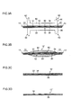
- Figs. 3A to 3D are explanatory views of the comparative examples 1 to 4.
- Fig. 4 is an explanatory view of the effect of the circuit device 10 shown in Fig. 1 in the form of a table that indicates the evaluation result of an evaluation experiment described below.
- a region other than the peripheral portion 24 of the circuit board 12 in the example and the comparative examples 1 to 4 refers to a region with the wiring pattern formed thereon (a region where the wiring layer 32 is not removed).
- the circuit device 10 described in the foregoing can be applied as a device which supports a printed-circuit board used for various applications, and as a device which protects the printed-circuit board.
- a tube made of polyvinyl chloride (PVC) (10 millimeters in diameter) is applied as the guiding member 16 (see Fig. 1 ). A part of a peripheral portion of the tube is cut open along a central axis to form a notch portion (shown in Fig. 1 with reference numeral 18).
- PVC polyvinyl chloride
- Respective sides of the circuit board 12 are inserted into the notch portion 18, so that all the end faces of the circuit board 12 are coated with the guiding member 16 (see Fig. 6 ).
- a contact interface between the surface (surface having the wiring layer 32 formed thereon and being covered with the insulating layer 34) of the circuit board 12 and the guiding member 16, and a contact interface between the back surface of the circuit board 12 and the guiding member 16 are sealed with adhesives provided thereto.
- the circuit board 12 with the guiding member 16 mounted thereon is put in an unshown constant temperature/constant humidity chamber (85°C, 85% (RH)) and a direct voltage of 12 volts is applied thereto.
- Dry gas 85°C, 25% (RH)
- RH constant temperature/constant humidity environment
- circuit board 12 shown in Fig. 2 is used as a printed-circuit board.
- a sealing member 56 is mounted on a part other than the peripheral portion 24 so as to remain the peripheral portion 24 (in the vicinity of the end face 14) of a surface 50 and a back surface 52 of the circuit board 12.
- the sealing member 56 has a space portion 58 formed in the inside and has flow channel portions 60 and 62 formed so as to communicate with the space portion 58.
- the circuit board 12 with the sealing member 56 mounted thereon is put in the constant temperature/constant humidity chamber (85°C, 85% (RH)) under the environment conditions set same as those in the example, and a direct voltage of 12 volts is applied to the wiring layer 32.
- Dry gas 85°C, 25% (RH)
- RH constant temperature/constant humidity environment
- the end face 14 and the peripheral portion 24 of the circuit board 12 were put in the high-humidity environment (85% (RH)), while other sections other than the end face 14 and the peripheral portion 24 of the circuit board 12 were put in the low-humidity environment (25% (RH)).
- a circuit board 12' is applied in the comparative example 2, in which a section other than the peripheral portion 24 of the surface 50 and the back surface 52 of the circuit board 12 shown in Fig. 2 is coated with water glass 64.
- the circuit board 12' which is coated with the water glass 64 except the peripheral portion 24 is put in the constant temperature/constant humidity chamber (85°C, 85% (RH)) under the environment conditions set same as those in the example, and a direct voltage of 12 volts is applied to the wiring layer 32.
- the constant temperature/constant humidity chamber 85°C, 85% (RH)
- the circuit board 12 shown in Fig. 2 is applied in the comparative example 3, though this circuit board 12 does not have the guiding member 16 mounted thereon.
- the circuit board 12 is put in the constant temperature/constant humidity chamber (85°C, 85% (RH)) under the environment conditions set same as those in the example, and a direct voltage of 12 volts is applied to the wiring layer 32.
- a circuit board 12" with the insulating layer 34 of the circuit board 12 shown in Fig. 2 being detached (the wiring layer 32 being exposed) is applied.
- the circuit board 12" does not have the guiding member 16 mounted thereon, and is put in the constant temperature/constant humidity chamber (85°C, 85% (RH)) under the environment conditions set same as those in the example, and a direct voltage of 12 volts is applied to the wiring layer 32.
- the comparative example 1 As compared with this, in the comparative example 1, occurrence of a failure (short circuit) was confirmed after 56 days of use of the circuit board 12. This indicates that the comparative example 1 may have a possibility of attaining a short-term reliability but has difficulty in attaining a long-term reliability.
- the circuit board 12 When an attention is focused on a difference between the example and the comparative example 1 in particular, the circuit board 12 is put in the dry state in both the example and the comparative example 1. However, the end face 14 of the circuit board 12 is dried in the example, whereas in comparative example 1, a region other than the peripheral portion 24 is dried among the surface 50 and the back surface 52 (principal surface) of the circuit board 12.
- the comparative example 1 is largely different from the example in the point that the circuit board 12 in the comparative example 1 is configured with susceptibility to water intrusion since the end face 14 of the circuit board 12 is exposed at the end of the base material 30 and at the end of the insulating layer 34.
- Figs. 5 to 7 are explanatory views of other aspects of the guiding member 16 shown in Fig. 1 .
- portions which are the same as or similar to those in Figs. 1 and 2 are designated with the same reference numerals and further explanation thereof is omitted here.
- illustration of the wiring layer 32 and the insulating layer 34 of the circuit board 12 is omitted.
- the guiding member 16' has a length and a shape corresponding to one side of the circuit board 12.
- dry gas is brought into contact with at least a part of the end face 14 of the circuit board 12, which corresponds to a region having particularly high possibility of being high in humidity, so that an intrusion of water to the inside of the circuit board 12 can be prevented.
- a guiding member 16" shown in Fig. 6 has an overall length corresponding to the length of the entire periphery of the circuit board 12, and is configured to have the ends 20 and 22 of Fig. 1 being connected to each other so as to have a shape, as a whole, similar to the plane shape of the circuit board 12.
- the guiding member 16" shown in Fig. 6 includes an inlet port 70 and an outlet port 72 for dry gas, which are provided at opposite angle positions on the peripheral portion.
- the circuit board 12 is interposed in between two plate-like members 76 and 78, and dry gas is introduced to between the plate-like member 76 and the plate-like member 78.
- end faces 80 and 82 of the plate-like members 76 and 78 protrude outward from the end face 14 of the circuit board 12, and a space between the plate-like members 76 and 78 functions as a flow channel of dry air.
- dry gas may be blown to the end face 14 of the circuit board 12 from the position opposite to the end face 14 of the circuit board 12, or dry gas may be passed along the end face 14 of the circuit board 12.
- one of the plate-like members 76 and 78 may be configured to have a box shape, so that the circuit board 12 is completely covered.
- the end faces 80 and 82 of the plate-like members 76 and 78 protrude outward from all the four end faces 14 of the circuit board 12 in the aspect shown in Figs. 7A and 7B , the end faces 80 and 82 of the plate-like members 76 and 78 have only to protrude outward from at least one face, out of the four end faces 14 of the circuit board 12.
- the plane shape of the circuit board 12 is not limited to a square shape.
- circuit boards having various plane shapes such as polygonal shapes other than the square shape, circular shapes, and complicated shapes having vertical angles including obtuse angles and acute angles.
- a publicly known dehumidification apparatus is applicable as a device which generates dry gas.
- the dehumidification apparatus 19 ( Fig.1 ) explained above can be adopted in this embodiment.
- a dry gas channel member which is connected to a dry gas inflow port in the guiding member 16 (16', 16", 74). Dry gas is supplied to the inside of the guiding member 16 from the air dryer through the dry gas channel member.
- the periphery of the end face 14 of the circuit board 12 can be dehumidified.
- an intrusion of water from the end face 14 of the circuit board 12 to the inside of the circuit board 12 is prevented by bringing the "dried body", such as dry gas, a liquid-state drying agent (for example, sulfuric acid, ethylene glycol, etc.), and a solid-state drying agent, into contact with the end face 14 of the circuit board 12.
- a liquid-state drying agent for example, sulfuric acid, ethylene glycol, etc.
- the guiding member 16 which has mainly a ring-like sectional shape was shown in this embodiment, various plane shapes, such as polygonal shapes including a square, and complicated shapes having vertical angles including obtuse angles and acute angles, are applicable as the sectional shape of the guiding member 16.
- a dried body is introduced into a space between the guiding member 16 and the end face 14 of the circuit board 12, and movement of the dried body is guided by the guiding member 16, so that the dried body can be brought into contact with the end face 14 of the circuit board 12, and an intrusion of water to the inside of the board is prevented by maintaining the periphery of the end face 14 of the circuit board 12 in a dry state.
- circuits such as an ASIC (Application Specific Integrated Circuit), active elements such as a transistor, passive elements such as a resistor, and connecting members such as a connector may be mounted.
- ASIC Application Specific Integrated Circuit
- the wiring layer 32 may be formed on both the surfaces of the base material 30, or a plurality of the wiring layers 32 and the insulating layers may alternately be laminated to constitute a multilayer structure.
- Configuration examples of the electric connection between wiring layers include those using a through hole and a via.
- An inkjet head which is configured to eject liquid, such as ink, from a plurality of nozzles formed on an ink ejection surface (nozzle surface), may have a flexible wiring board disposed in the vicinity of the nozzle surface or in the vicinity of a channel structure.
- the vicinity of the nozzle surface and the vicinity of the channel structure may be in an environment higher in humidity than other regions. Accordingly, there is concern about occurrence of a failure attributed to electrochemical migration of the flexible wiring board.
- Fig. 8 is a perspective view showing a schematic configuration of an inkjet head assembly constituting a full line type inkjet head. It is possible to constitute a long line type inkjet head by connecting a plurality of the inkjet head assemblies 100 shown in Fig. 8 .
- the inkjet head assembly 100 is configured so that a single inkjet head assembly 100 can also function as an inkjet head, the inkjet head may be constituted from only one inkjet head assembly 100.
- the inkjet head assembly 100 shown in Fig. 8 includes a head body 102, a pair of flexible wiring boards (circuit boards) 104, a pair of mounting frames 106, and the like. As shown in Fig. 8 , the flexible wiring board 104 is supported while being interposed in between the head body 102 and the mounting frame 106.
- the head body 102 includes an ejection die 108 provided on a lowermost portion, and tube connecting nozzles 110 provided on an upper most portion.
- One out of the two tube connecting nozzles 110 is for ink supply, while the other is for ink collection.
- the tube connecting nozzle 110 for ink supply is made to communicate with an ink supply tank via an ink tube.
- the tube connecting nozzle 110 for ink collection is made to communicate with an ink collection tank via an ink tube.
- the flexible wiring board 104 has a wiring (copper wiring) (shown in Fig. 14 with reference numeral 170) formed as a transmission line of a control signal (command signal) sent out from an unshown control circuit. Note that a wiring for transmitting other signals, such as a sensor signal, may be formed.
- An opening 112 that communicates with a dry gas channel (not shown in Fig. 8 , shown in Fig. 9 with reference numeral 124) that is formed inside the mounting frame 106 is formed at two places on the mounting frame 106, and a recess portion (not shown in Fig. 8 , shown in Fig. 9 with reference numeral 122) corresponding to the thickness of the flexible wiring board 104 is further formed.
- a mounting portion 114 is also formed on the mounting frame 106, the mounting portion 114 being used for supporting and positioning purposes at the time of combining a plurality of the inkjet head assemblies 100.
- Fig. 9 is an exploded perspective view of the inkjet head assembly 100 shown in Fig. 8 .
- portions which are the same as or similar to those described in the foregoing are designated with the same reference numerals and further explanation thereof is omitted here.
- the surface of the mounting frame 106 which comes into contact with the flexible wiring board 104, has a recess portion 122 formed to have a depth corresponding to the thickness of the flexible wiring board 104 for housing the flexible wiring board 104.
- a peripheral portion of the recess portion 122 forms a groove portion 124 deeper than other portions, the groove portion 124 functioning as a dry gas channel.
- the groove portion 124 is filled with the dry gas, so that the dry gas can be brought into contact with the end face 126 of the flexible wiring board 104.
- the dry gas described before can be applied as the dry gas.
- a liquid or solid dried body may also be applied.
- Adhesives are used for joining between the head body 102 and the mounting frame 106, and for joining between the flexible wiring board 104 and the mounting frame 106.
- Fig. 10 is a perspective view of the ejection die 108 shown in Figs. 8 and 9 .
- the ejection die 108 is made of a plate-like member having a parallelogram plane shape, with an ink channel (not shown in Fig. 10 , shown in Fig. 11 with reference numeral 146) formed inside the ejection die 108.
- Driving ICs 132 are mounted on an upper surface 130 of the ejection die 108, where an electrical wiring (not shown in Fig. 11 , shown in Fig. 12 with reference numeral 152), which is connected to an input output terminal (not shown) of each driving IC 132, and a connection terminal portion 134, which is electrically connected to the electrical wiring and which is connected to the flexible wiring board 104, are formed.
- a hole illustrated in Fig. 10 with reference numeral 136 is an ink channel opening.
- Fig. 11 is a fragmentary sectional view of the inkjet head assembly shown in Fig. 8 , in the state where the flexible wiring board 104 and the mounting frame 106 are mounted on the head body 102.
- a nozzle 140 for ejecting ink As shown in Fig. 11 , there are formed in the ejection die 108, a nozzle 140 for ejecting ink, a pressure chamber 142 for housing the ink to be ejected from the nozzle 140, a diaphragm 144 used as a ceiling surface of the pressure chamber 142, and a supply channel 146 for supplying the ink to the pressure chamber 142.
- the supply channel 146 is made to communicate with a supply-side filter housing (not shown in Fig. 11 , shown in Fig. 13 with reference numeral 162).
- a circulation channel 147 which branches from the nozzle 140 is made to communicate with a collection-side filter housing (not shown in Fig. 11 , shown in Fig. 13 with reference numeral 164).
- a piezoelectric element 148 is provided on the surface of the diaphragm 144 which is opposite to the pressure chamber 142, and a top electrode (not shown) of the piezoelectric element 148 is electrically connected to the driving IC 132 via the electrical wiring.
- the diaphragm 144 When a drive voltage is applied from the driving IC 132 to the piezoelectric element 148, the diaphragm 144 is deformed corresponding to flexural deformation of the piezoelectric element 148, so that the ink of a volume corresponding to a decreased volume of the pressure chamber 142 is ejected from the nozzle 140.
- the piezoelectric element 148 is restored to a stabilizing state, the volume of the pressure chamber 142 is restored to the original volume (shape), and the ink is charged into the pressure chamber 142 via the supply channel 146.
- the circulation channel 147 is a channel for circulating ink in the vicinity of the nozzle 140. By suitably circulating the ink in the vicinity of the nozzle 140, thickening of the ink in the vicinity of the nozzle 140 is prevented and a clogging of the nozzle 140 is avoided.
- the flexible wiring board 104 is curved toward the upper surface 130 of the ejection die 108 in the vicinity of the upper surface 130 of the ejection die 108 and is joined to the connection terminal portion 134 formed on the upper surface 130 of the ejection die 108.
- connection terminal portion 134 is joined to the flexible wiring board 104, a support body 138, or the like, is mounted on the ejection die 108 to complete the head body 102.
- the flexible wiring board 104 and the recess portion 122 of the mounting frame 106 are aligned, and in the state where the flexible wiring board 104 is housed in the recess portion 122 of the mounting frame 106, the mounting frame 106 is mounted on the head body 102.
- Fig. 12 is an explanatory view of a connecting configuration between the ejection die 108 and the flexible wiring board 104. As shown in Fig. 12 , the connection terminal portion 150 is formed on the flexible wiring board 104, and the connection terminal portion 150 is joined to the connection terminal portion 134 of the ejection die 108.
- a joining member having conductivity such as a solder and an electrically conductive adhesive, is used for joining between the connection terminal portion 150 of the flexible wiring board 104 and the connection terminal portion 134 of the ejection die 108.
- the ink channel opening 136 and the piezoelectric element 148 are provided, and the electrical wiring 152 is formed for transmitting a drive voltage which is applied to the piezoelectric element 148.
- the piezo-electric method using flexural deformation of the piezoelectric element 148 was shown as an ink ejection method of the inkjet head assembly 100 in this embodiment, it is also possible to apply other ejection methods, such as a thermal method which heats ink in the pressure chamber 142 with a heater provided inside the pressure chamber (liquid chamber) 142 and ejects the ink by utilizing a film boiling phenomenon.
- a thermal method which heats ink in the pressure chamber 142 with a heater provided inside the pressure chamber (liquid chamber) 142 and ejects the ink by utilizing a film boiling phenomenon.
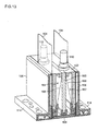
- Fig. 13 is a cross sectional view of the inkjet head assembly shown in Fig. 8 .
- the head body 102 has a supply-side filter housing 162 provided on one side and a collection-side filter housing 164 provided on the other side across a divider plate 160.
- the respective filter housings 162 and 164 house filters 166 and 168 made of stainless steel in a diagonal direction of respective chambers.
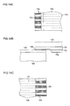
- Fig. 14A is a bottom view of the flexible wiring board 104
- Fig. 14B is a cross sectional view of the ejection die 108 and the flexible wiring board 104 in a connected state
- Fig. 14C is a plan view of the ejection die.
- the flexible wiring board 104 is configured so that an insulating layer made of polyimide (shown in Fig. 14B with reference numeral 174) is provided with a copper wiring 170 (shown with a broken line), and a region excluding the connection terminal portion 150 is bonded to a protective layer made of polyimide (shown in Fig. 14B with reference numeral 178) via an adhesive layer (shown in Fig. 14B with reference numeral 176).
- the insulating layer 174 in the flexible wiring board 104 applied in this embodiment has a thickness of 25 micrometers, while the adhesive layer 178 has a thickness of 17.5 micrometers.
- the copper wiring 170 As the copper wiring 170, a copper alloy may be applied, and other metallic materials having high electric conductivity, such as gold, may also be applied.
- the copper wiring 170 in the flexible wiring board 104 applied in this embodiment has a thickness of 12 micrometers.
- each connection terminal 172 in the connection terminal portion 150 of the flexible wiring board 104 is plated with solder, gold, and tin to facilitate connection to the connection terminal portion 134 of the ejection die 108.
- the plated material dissolves at the time of joining by heat pressing, so that each connection terminal 172 in the connection terminal portion 150 of the flexible wiring board 104 is integrated with each connection terminal (shown in Fig. 14C with reference numeral 182) in the connection terminal portion 134 of the ejection die 108.
- connection terminal portion 150 (see Fig. 14A ) of the flexible wiring board 104 is joined to the connection terminal portion 134 (see Fig. 14C ) of the ejection die 108.
- soldering by heat pressing is applied.
- a copper ion diffusion suppression coating 180 is formed on the flexible wiring board 104. Then, the connection terminal portion 150 of the flexible wiring board 104 is aligned with the connection terminal portion 134 of the ejection die 108, and as shown in Fig. 14B , the flexible wiring board 104 and the ejection die 108 are joined together.
- FIG. 15 is a perspective view showing an internal configuration of the mounting frame 106.
- the flexible wiring board 104 in a housed state is shown with a dashed line.
- the flexible wiring board 104 in the housed state is curved toward the near side on the page, and is joined to the ejection die 108 (see Fig. 11 ).
- the mounting frame 106 shown in Fig. 15 has the recess portion 122 provided on the surface which faces the head body 102 (see Fig. 13 ).
- the recess portion 122 has a shape corresponding to the shape of the flexible wiring board 104, has a size slightly smaller than the size of the flexible wiring board 104, and has a depth corresponding to the thickness of the flexible wiring board 104.
- Two vertical groove portions 190 and one horizontal groove portion 192 (in Fig. 9 , the vertical groove portions 190 and the horizontal groove portion 192 are generically referred to as the groove portion which is designated with reference numeral 124) which function as a dry gas channel are formed on the periphery of the recess portion 122.
- the opening 112 is formed at an upper end of each vertical groove portion 190 and is made to communicate with the horizontal groove portion 192 at the lower end.
- a space is formed in the periphery of the end face 126 of the flexible wiring board 104. If dry air is introduced from the opening 112 in this state, the space formed in the periphery of the end face 126 of the flexible wiring board 104 is filled with the dry air, so that the dry air can be brought into contact with the end face 126 of the flexible wiring board 104.
- FIGs. 16A and 16B are perspective views showing another internal configuration example of the mounting frame 106 shown in Fig. 15 .
- a mounting frame 106' shown in Figs. 16A and 16B has a dual structure having a first mounting frame 194 (first guiding member) that functions as a flexible wiring board support member and a second mounting frame 196 (second guiding member) that has a dry gas introduction channel formed thereon.
- first mounting frame 194 On the first mounting frame 194, a lower end portion (shown with reference numeral 190') of the vertical groove portion 190 shown in Fig. 15 and the horizontal groove portion 192 are formed. There is also formed a first dry gas introduction channel 198 (through hole) which penetrates the first mounting frame 194 in a thickness direction and which communicate with at least one of the vertical groove portion 190' and the horizontal groove portion 192.
- a second dry gas introduction channel 199 (hole) is formed at a position corresponding to the first dry gas introduction channel 198, and the second dry gas introduction channel 199 communicates with an unshown dry gas inlet port.
- a liquid-state dried body and a solid-state dried body may suitably be applied in place of or in combination with the dry gas.
- Fig. 17 is a perspective plan view showing a nozzle arrangement of the inkjet head assembly 100.
- Fig. 17 is a view of the surface on which ejected liquid is deposited as viewed from the inkjet head assembly 100.
- the inkjet head assembly 100 is configured to have nozzles 140 arranged in a two-dimensional way.
- the inkjet head having such an arrangement of the nozzles 140 is called a matrix head.
- the inkjet head assembly 100 shown in Fig. 17 is configured to have a large number of the nozzles 140 arrayed along a column direction W having an angle ⁇ with respect to a sub-scanning direction Y and along a row direction V having an angle ⁇ with respect to a main scanning direction X, and substantially has high-density (for example, 1200 dots per inch) nozzle arrangement in the main scanning direction X.
- a nozzle group (nozzle row) arrayed along the row direction V is illustrated and designated with reference numeral 200
- a nozzle group (nozzle column) arrayed along the column direction W is illustrated and designated with reference numeral 202.
- the nozzle arrangement applicable to the present invention is not limited to the nozzle arrangement shown in Fig. 17 .
- the nozzle arrangement is also applicable to an aspect in which a plurality of nozzles are arrayed in a matrix form along the row direction in the main scanning direction and along the column direction which is slant with respect to the main scanning direction.
- Fig. 18 is a plan view showing a configuration example of an inkjet head constituted of a plurality of the inkjet head assemblies 100 which are connected to each other.
- An inkjet head 210 shown in Fig. 18 is a multi head constituted of a plurality of the inkjet head assemblies 100 connected in one line. It is also possible to constitute a multi head by arranging the inkjet head assemblies 100 in a staggered form.
- Application examples of the multi head constituted of a plurality of the inkjet head assemblies 100 include a full line-type head which corresponds to the overall width of a recording medium.
- the full line-type head is configured to have a plurality of nozzles (shown in Fig. 11 with reference numeral 140) arrayed along a direction (main scanning direction) orthogonal to a moving direction (sub-scanning direction) of the recording medium, corresponding to the length (width) of the recording medium in the main scanning direction.
- An image can be formed over the entire surface of the recording medium by a so-called single pass image recording method which carries out image recording with only one scanning action which is relatively conducted by the above-configured inkjet head 210 and the recording medium.
- the inkjet head 210 shown in this embodiment is widely applicable to apparatuses which support the inkjet method, such as an inkjet recording apparatus which forms a color image on a recording medium, and a liquid ejection apparatus which ejects functional liquid on a substrate to form a mask pattern and an electrical wiring pattern.
- the inkjet recording apparatus includes a recording medium conveyance device which relatively conveys an inkjet head and a recording medium; an ejection control unit which controls ink ejection from the inkjet head, an image processing unit which generates ink ejection data based on input image data, and a driving signal generation unit which generates a driving signal applied to the inkjet head based on ejection data.
- This configuration example may further include a dry gas generation unit previously explained and a dry gas channel member used as a dry gas channel, so that dry gas is supplied from the dry gas generation unit to the inkjet head via the dry gas channel member.
- the flexible wiring board is applied as a transmission member for transmitting signals, such as a control signal sent from a control system provided in the outside of the inkjet head to the inkjet head, and a detection signal sent from sensors of the inkjet head to the control system.
- the flexible wiring board as an electrical wiring which transmits an electrical signal between the inkjet head and the outside, the space for disposing the electrical wiring can be saved.
- the wiring 170 which transmits a driving signal (control signal) which is applied to a piezoelectric element that functions as a pressure generation element at the time of ejection operation, is formed on the flexible wiring board 104, and dry air is brought into contact with the end face 126 of the flexible wiring board 104. Accordingly, even when the flexible wiring board 104 is placed under a high-humidity environment in the vicinity of the nozzle and in the vicinity of the flow channel, a short circuit between wirings, attributed to electrochemical migration caused by an intrusion of water to the inside of the flexible wiring board 104, is prevented.
- Drying performance in the circuit device and in the inkjet head assembly described in the forgoing may be controlled by adjusting a flow rate of the dry gas so as to attain a preset humidity, or by providing a moisture sensor to adjust the flow rate so as to attain a humidity set based on the detection result.
- a circuit device including: a circuit board which has one or more wiring layers formed on a base material and has an insulating layer laminated on a surface of the one or more wiring layers opposite to the base material; and a guiding member which is configured to encircle at least a part of an end face of the circuit board so that a space is formed with the end face and to guide movement of a dried body which is supplied to the formed space.
- the dried body is brought into contact with the end of the circuit board while movement of the dried body is guided by the guiding member, so that an intrusion of water (moisture) to the inside from the end face of the circuit board is prevented, and occurrence of a failure attributed to a short circuit between wirings resulting from electrochemical migration is prevented.
- the dried body which is a concept including a gas, a liquid, and a solid, has a function of keeping the atmosphere on the end face of the circuit board in a dry state.
- the aspect is applicable to all the single-sided board in which a wiring layer is formed only on one surface of the base material, the double-sided board in which a wiring layer is formed on both one surface of the base material and the other surface which is opposite to the one surface, and the multilayer board which includes a plurality of wiring layers and an insulating layer formed between the respective wiring layers.
- the dry fluid is brought into contact with the end face of the circuit board, so that the atmosphere on the end face of the circuit board is maintained in a dry state.
- Dry fluid is a concept including a gas and a liquid, and examples of the dry fluid include a gas in a low humidity state.
- the atmosphere on the end face of the circuit board is maintained in a dry state.
- the inside of the hollow structure i.e., the circumferential atmosphere on the end face of the circuit board is maintained in a dry state.
- circuit device The circuit device according to any of the first to fourth aspects, wherein the circuit board has a polygonal plane shape, and the guiding member is configured to cover at least one side out of a plurality of sides of the circuit board.
- the dried body can be brought into contact with the entire periphery of the end face of the circuit board, the entire periphery of the end face of the circuit board can be maintained in a desirable dry state.
- the guiding member includes a plurality of members which sandwich the circuit board from one surface of the circuit board and from the other surface opposite to the one surface, and at least a part of the end face of the plurality of members is configured to protrude outward from the end face of the circuit board.
- a plurality of members are formed into plate-like members.
- one member is a plate-like member while the other member is a box-like member so that the entire circuit board is covered.
- the double-sided board which includes a wiring layer provided on both the surfaces of the base material and an insulating layer that is laminated on the wiring layer, an intrusion of water (moisture) to the inside from the end face of the circuit board is prevented, and occurrence of a failure attributed to a short circuit between wirings resulting from electrochemical migration is prevented.
- the multilayer board which includes a plurality of wiring layers laminated and a layer for insulation formed between the respective wiring layers, an intrusion of water (moisture) to the inside from the end face of the circuit board is prevented, and occurrence of a failure attributed to a short circuit between wirings resulting from electrochemical migration is prevented.
- the plurality of wiring layer may be layered in vertical direction.
- a layer for insulation may be the insulating layer according to any of the above one to eighth aspects.
- An inkjet head assembly constituting an inkjet head which is provided with nozzles for ejecting liquid, the inkjet head assembly comprising: an electrical wiring; an extraction electrode which is electrically connected to the electrical wiring; and a circuit device which includes a circuit board joined to the extraction electrode, wherein the circuit device is a circuit device according to any one of the above one to ninth aspects.
- the circuit board is disposed in a high-humidity environment, such as in the vicinity of a liquid ejection unit and in the vicinity of a liquid channel portion, bringing the dried body into contact with the end face of the circuit board makes it possible to maintain a desirable dry state, so that an intrusion of water (moisture) to the inside from the end face of the circuit board is prevented, and occurrence of a failure attributed to a short circuit between wirings resulting from electrochemical migration is prevented.
- a high-humidity environment such as in the vicinity of a liquid ejection unit and in the vicinity of a liquid channel portion
- the inkjet head assembly is configured so that a single inkjet head assembly may function as an inkjet head and also a plurality of inkjet head assemblies may be connected to constitute an inkjet head.
- the inkjet head assembly according to the tenth aspect, further including: a liquid chamber which is configured to communicate with the nozzles; and a pressure application element which is configured to apply pressure to liquid housed in the liquid chamber, wherein the electrical wiring is configured to transmit a driving signal for operating the pressure application element.
- Examples of the pressure application element in the aspect include a piezoelectric element which is flexurally deformed by application of a drive voltage.
- the inkjet head assembly according to the eleventh aspect, further including; a main body unit which is configured to have the liquid chamber formed therein; and a support member which is configured to support the main body unit, wherein the circuit board is configured to be supported by the support member between the main body unit and the support member, the support member is configured to also function as the guiding member, and a groove portion is formed on a surface which comes into contact with the circuit board as a space which guides movement of the dried body.
- a groove or a recess portion is formed inside the support member and is used as a housing portion of the circuit board or as a passage of the dried body.
- the inkjet head assembly according to the twelfth aspect, wherein the guiding member which is configured to also serve as the support member includes: a first guiding member (194) on which the groove portion is formed to encircle a part of a periphery of the circuit board, and which has a through hole formed to communicate with the groove portion and penetrate in a thickness direction; and a second guiding member which is configured to have a hole formed to communicate with the through hole.
- an aspect of forming on the first guiding member a housing portion for housing the circuit board separately from the groove portion that serves as the passage of the dried body is preferable.
- an aspect of forming the groove portion of the first guiding member corresponding to a position which is particularly in a high-humidity state is preferable.
- circuit board is a flexible wiring board which uses a resin film as the base material so as to have flexibility.
- the circuit board may be disposed in a clearance formed in the inkjet head assembly configuration, so that the space between the inkjet head assembly and the outside for disposing electrical wiring may be saved.
Landscapes
- Engineering & Computer Science (AREA)
- Microelectronics & Electronic Packaging (AREA)
- Non-Metallic Protective Coatings For Printed Circuits (AREA)
- Particle Formation And Scattering Control In Inkjet Printers (AREA)
- Manufacturing Of Printed Wiring (AREA)
Abstract
Description
- The present invention relates to a circuit device and an inkjet head assembly, and more particularly relates to a technology for protecting an electrical wiring pattern on a circuit board.
- There is known a circuit board configured to include a base material, such as a resin film and glass epoxy, a thin film made of a metallic material, such as copper, formed on the base material, an electrical wiring pattern formed by patterning the metal film by etching or other methods, and further a coating made of an insulating material, such as a solder resist, for coating the electrical wiring pattern.
- The circuit board is widely used in industrial equipment and/or consumer equipment. Thus, as the circuit board is used in various applications and environments, the use environments of the circuit board are assumed to include a high-humidity environment, a high-temperature environment, and an environment where foreign materials, such as powder dust, are present.
- Such environments may cause a problem of a short circuit or an open circuit between electrical wirings due to degradation of insulating materials and a problem of a short circuit of the electrical wiring caused by water and foreign materials intruding in between an insulating layer and a base material.
- In general, when the circuit board is used in the high-humidity environment and the environment involving a large amount of foreign materials (materials having conductivity in particular), long-term reliability (resistance) becomes an issue. Since an electrical wiring pattern is coated with an insulating material in order to prevent a short circuit and an open circuit of the electrical wiring pattern, the reliability is not an issue in a short term use. However, in the case where the circuit board is used over a long period of time, further measures need to be taken in a viewpoint of assuring long-term reliability.
- Described in Japanese Patent Application Laid-Open No.
2010-86992 - Such configuration suppresses an intrusion of water into the coating layer and prevents a short circuit between the conductive patterns.
- However, while the circuit device described in Japanese Patent Application Laid-Open No.
2010-86992 - The term "electrochemical migration" herein refers to a phenomenon in which ion migration is generated and grown, due to an electrochemical phenomenon, in an originally sufficient insulating material in a printed board or the like in the state of receiving application of electric bias voltage, as a result of which a short circuit occurs between electrodes and between wirings.
- The present invention has been made in view of such circumstances, and it is an object of the present invention to provide a circuit device and an inkjet head assembly capable of preventing occurrence of a failure attributed to a short circuit and the like of the circuit board even in the case of being used for a long period of time under a relatively high-humidity environment.
- In order to accomplish the above object, a circuit device according to the present invention includes: a circuit board which has one or more wiring layers formed on a base material and has an insulating layer laminated on a surface of the one or more wiring layers opposite to the base material; and a guiding member which is configured to encircle at least a part of an end face of the circuit board so that a space is formed with the end face and to guide movement of a dried body which is supplied to the formed space.
- According to the present invention, the dried body is brought into contact with the end portion of the circuit board while movement of the dried body is guided by the guiding member. This makes it possible to prevent an intrusion of water (moisture) to the inside from the end face of the circuit board, and to prevent occurrence of a failure attributed to a short circuit between wirings resulting from electrochemical migration.
-
-
Fig. 1 is a schematic configuration view of a circuit device according to an embodiment of the present invention; -
Fig. 2 is a cross sectional view showing a configuration example of the circuit board shown inFig. 1 ; -
Fig. 3A is an explanatory view of a comparative example 1,Fig. 3B is an explanatory view of a comparative example 2,Fig. 3C is an explanatory view of a comparative example 3, andFig. 3D is an explanatory view of a comparative example 4; -
Fig. 4 is an explanatory view of an operational effect of the circuit device shown in the present embodiment; -
Fig. 5 is an explanatory view of another aspect of a guiding member shown inFig. 1 ; -
Fig. 6 is an explanatory view of another aspect of the guiding member shown inFig. 1 ; -
Figs. 7A and 7B are explanatory views of another aspect of the guiding member shown inFig. 1 ; -
Fig. 8 is a perspective view showing a schematic configuration of an inkjet head assembly according to an embodiment of the present invention; -
Fig. 9 is an exploded perspective view of the inkjet head assembly shown inFig. 8 ; -
Fig. 10 is a perspective view of an ejection die; -
Fig. 11 is a fragmentary sectional view of the inkjet head assembly shown inFig. 8 ; -
Fig. 12 is an explanatory view of a connecting configuration between the ejection die and a flexible wiring board; -
Fig. 13 is a cross sectional view of the inkjet head assembly shown inFig. 8 ; -
Fig. 14A is a bottom view of the flexible wiring board,Fig. 14B is a cross sectional view of the ejection die and the flexible wiring board in a connected state, andFig. 14C is a plan view of the ejection die; -
Fig. 15 is a perspective view showing an internal configuration of a mounting frame ofFig. 9 ; -
Figs. 16A and 16B are perspective views showing another internal configuration example of the mounting frame ofFig. 15 ; -
Fig. 17 is a plan view showing nozzle arrangement of an inkjet head assembly; and -
Fig. 18 is a plan view showing a configuration example of an inkjet head constituted of a plurality of inkjet head assemblies connected to each other. - Hereinafter, an embodiment for carrying out the present invention is described in detail with reference to the accompanying drawings.
-
Fig. 1 is a schematic configuration view of a circuit device according to an embodiment of the present invention. Acircuit device 10 shown inFig. 1 includes acircuit board 12 and a guidingmember 16 for guiding movement of dry gas so as to bring the dry gas into contact with anend face 14 of thecircuit board 12. - As described later in detail, the
circuit board 12 is configured to have a wiring layer (not shown inFig. 1 , shown inFig. 2 with reference numeral 32) coated with an insulating layer (not shown inFig. 1 , shown inFig. 2 with reference numeral 34), and theend face 14 is exposed at the end of the base material, at the end of the wiring layer, and at the end of the insulating layer. - The term "end face" of the
circuit board 12 herein refers to a surface which intersects (which is orthogonal to) an insulating layer forming surface. - The guiding
member 16 has a hollow structure in a cylindrical shape, and has anotch portion 18 formed for sandwiching thecircuit board 12. More specifically, the guidingmember 16 has a ring shaped cross section with a part of the ring shape being missing. - In the aspect shown in
Fig. 1 , three sides of theend face 14, out of four sides of theend face 14 of thecircuit board 12 which has a square plane shape, are covered with the guidingmember 16. Dry gas is supplied from oneend 20 or theother end 22 of the guidingmember 16 to the inside of the guidingmember 16 so that the dry gas is filled in the guidingmember 16. The guidingmember 16 guides movement of the dry gas so as to bring the dry gas into contact with theend face 14 of thecircuit board 12 covered with the guidingmember 16. - In the
circuit device 10 shown in this embodiment, at least a part of theend face 14 of thecircuit board 12 needs to be covered with the guidingmember 16. Accordingly, as shown inFig. 1 , it is possible to adopt the configuration in which aperipheral portion 24 of thecircuit board 12 is covered with the guidingmember 16. - A width of the
peripheral portion 24 of the circuit board 12 (an area of theperipheral portion 24 of thecircuit board 12, a region covered with the guidingmember 16 as theperipheral portion 24 of the circuit board 12) may be determined from a viewpoint of mounting of the guidingmember 16, or be determined from a viewpoint of the configuration (a wiring pattern forming region, etc.) of thecircuit board 12. For example, it is possible to define a region, from theend face 14 of thecircuit board 12 to a length of the thickness of the guidingmember 16, as theperipheral portion 24 from a viewpoint of mounting of the guidingmember 16, and it is possible to define a region where a wiring pattern is not formed (a non-wiring pattern forming region) as theperipheral portion 24 from a viewpoint of the configuration of thecircuit board 12. - The term "dry gas" herein refers to a gas which has a humidity at least less than the atmospheric humidity of the
circuit board 12. As the dry gas, mixture gas like air may be applied, or single gas may also be applied. - As shown in
Fig. 1 , the guidingmember 16 may have an opening formed on both theends ends member 16, dry gas is supplied from the opening on the oneend 20, and the dry gas having being in contact with theend face 14 of thecircuit board 12 is discharged from the opening on theother end 22, so that the dry gas is maintained in a sufficient dry state. - A publicly known dehumidification apparatus is applicable as a device which generates dry gas. For example, a
dehumidification apparatus 19 including acompressor 19A and anair dryer 19B, thecompressor 19A may be operated to send compressed air to theair dryer 19B, and theair dryer 19B may be operated to generate dry gas. Both refrigeration type and filter type air dryers are applicable as theair dryer 19B. Such configuration of thedehumidification apparatus 19 can be adopted in other aspects/embodiments explained below. -
Fig. 2 is a cross sectional view showing a configuration example of thecircuit board 12 shown inFig. 1 . In thecircuit board 12 shown inFig. 2 , thewiring layer 32 is formed on one surface of abase material 30, and thewiring layer 32 and asurface 36 of thebase material 30 with thewiring layer 32 formed thereon are coated with the insulatinglayer 34. - A surface 38 of the
base material 30, which is opposite to the surface having thewiring layer 32 formed thereon, may be coated with the insulatinglayer 34. - The end face 14 of the
circuit board 12 is exposed without being coated at the end of thebase material 30 and at the end of the insulatinglayer 34. - As the
base material 30, materials, such as a resin film, glass epoxy, paper (impregnated with phenol resin), and ceramics, are applicable. As the wiring layer, materials, such as copper, gold, silver, and platinum, which are high in electric conductivity and are patternable by etching, and the like, are applicable. As the insulatinglayer 34, insulating materials, such as epoxy resin (solder resist) having good insulation, are applicable. - In the
circuit device 10 shown in this embodiment, the dry gas is brought into contact with theend face 14 of thecircuit board 12, so that the atmosphere on theend face 14 of thecircuit board 12 and in the vicinity thereof is maintained in a dry state. More specifically, an intrusion of water (moisture) to the inside of thecircuit board 12 from theend face 14 of thecircuit board 12 along theinterface 36 between thebase material 30 and the insulatinglayer 34 is prevented. - By preventing the intrusion of water to the inside of the
circuit board 12, a failure due to electrochemical migration caused by water reaching thewiring layer 32 and a current passing to thewiring layer 32 is prevented. - A description is now given of the operational effect in the case (example) where dry gas is brought into contact with the end face 14 (see
Figs. 1 and 2 ) of thecircuit board 12 in comparison with comparative examples 1 to 4. -
Figs. 3A to 3D are explanatory views of the comparative examples 1 to 4.Fig. 4 is an explanatory view of the effect of thecircuit device 10 shown inFig. 1 in the form of a table that indicates the evaluation result of an evaluation experiment described below. - In the evaluation experiment, a period of time from the start of use of a printed-circuit board (start of application of voltage) to occurrence of a failure (short circuit) was examined under every environmental condition and printed-circuit board condition. As the printed-circuit boards for use in the example and in the comparative examples 1 and 3 (
Figs. 3A and 3C ), thecircuit board 12 shown inFig. 2 is applied. Other conditions are as explained below. - "A region other than the
peripheral portion 24 of thecircuit board 12" in the example and the comparative examples 1 to 4 refers to a region with the wiring pattern formed thereon (a region where thewiring layer 32 is not removed). - The
circuit device 10 described in the foregoing can be applied as a device which supports a printed-circuit board used for various applications, and as a device which protects the printed-circuit board. - As the guiding member 16 (see
Fig. 1 ), a tube made of polyvinyl chloride (PVC) (10 millimeters in diameter) is applied. A part of a peripheral portion of the tube is cut open along a central axis to form a notch portion (shown inFig. 1 with reference numeral 18). - Respective sides of the circuit board 12 (see
Fig. 1 ) are inserted into thenotch portion 18, so that all the end faces of thecircuit board 12 are coated with the guiding member 16 (seeFig. 6 ). - A contact interface between the surface (surface having the
wiring layer 32 formed thereon and being covered with the insulating layer 34) of thecircuit board 12 and the guidingmember 16, and a contact interface between the back surface of thecircuit board 12 and the guidingmember 16 are sealed with adhesives provided thereto. - The
circuit board 12 with the guidingmember 16 mounted thereon is put in an unshown constant temperature/constant humidity chamber (85°C, 85% (RH)) and a direct voltage of 12 volts is applied thereto. Dry gas (85°C, 25% (RH)) is supplied to the inside of the guidingmember 16 and is circulated therein so that a constant temperature/constant humidity environment of 85°C and 25% (RH) is maintained in the inside of the guidingmember 16. - As in the example described in the foregoing, the
circuit board 12 shown inFig. 2 is used as a printed-circuit board. - As shown in
Fig. 3A , a sealingmember 56 is mounted on a part other than theperipheral portion 24 so as to remain the peripheral portion 24 (in the vicinity of the end face 14) of asurface 50 and aback surface 52 of thecircuit board 12. - The sealing
member 56 has aspace portion 58 formed in the inside and hasflow channel portions space portion 58. - The
circuit board 12 with the sealingmember 56 mounted thereon is put in the constant temperature/constant humidity chamber (85°C, 85% (RH)) under the environment conditions set same as those in the example, and a direct voltage of 12 volts is applied to thewiring layer 32. Dry gas (85°C, 25% (RH)) is supplied to the inside of the sealingmember 56 and is circulated therein so that a constant temperature/constant humidity environment of 85°C and 25% (RH) is maintained in the inside of the sealingmember 56. - In other words, in the comparative example 1, the
end face 14 and theperipheral portion 24 of thecircuit board 12 were put in the high-humidity environment (85% (RH)), while other sections other than theend face 14 and theperipheral portion 24 of thecircuit board 12 were put in the low-humidity environment (25% (RH)). - As shown in
Fig. 3B , a circuit board 12' is applied in the comparative example 2, in which a section other than theperipheral portion 24 of thesurface 50 and theback surface 52 of thecircuit board 12 shown inFig. 2 is coated withwater glass 64. - The circuit board 12' which is coated with the
water glass 64 except theperipheral portion 24 is put in the constant temperature/constant humidity chamber (85°C, 85% (RH)) under the environment conditions set same as those in the example, and a direct voltage of 12 volts is applied to thewiring layer 32. - As shown in
Fig. 3C , thecircuit board 12 shown inFig. 2 is applied in the comparative example 3, though thiscircuit board 12 does not have the guidingmember 16 mounted thereon. Thecircuit board 12 is put in the constant temperature/constant humidity chamber (85°C, 85% (RH)) under the environment conditions set same as those in the example, and a direct voltage of 12 volts is applied to thewiring layer 32. - As shown in
Fig. 3D , acircuit board 12" with the insulatinglayer 34 of thecircuit board 12 shown inFig. 2 being detached (thewiring layer 32 being exposed) is applied. Thecircuit board 12" does not have the guidingmember 16 mounted thereon, and is put in the constant temperature/constant humidity chamber (85°C, 85% (RH)) under the environment conditions set same as those in the example, and a direct voltage of 12 volts is applied to thewiring layer 32. - No failure (short circuit) occurred during 90 days of use of the
circuit board 12 in the example, and therefore if current is continuously applied to thecircuit board 12 for a long period of time under the high-humidity/temperature environment, thecircuit board 12 has an extremely low chance of having a failure, which ensures long-term reliability. - As compared with this, in the comparative example 1, occurrence of a failure (short circuit) was confirmed after 56 days of use of the
circuit board 12. This indicates that the comparative example 1 may have a possibility of attaining a short-term reliability but has difficulty in attaining a long-term reliability. - In the comparative example 2, a failure (short circuit) occurred after 11 days of use of the circuit board 12', and in the comparative example 3, a failure (short circuit) occurred after 3 days of use of the
circuit board 12. Further, in the comparative example 4, a failure (short circuit) occurred immediately after the start of use of thecircuit board 12". In conclusion, it is presumed that under these conditions, even a short-term reliability is hard to achieve. - When an attention is focused on a difference between the example and the comparative example 1 in particular, the
circuit board 12 is put in the dry state in both the example and the comparative example 1. However, theend face 14 of thecircuit board 12 is dried in the example, whereas in comparative example 1, a region other than theperipheral portion 24 is dried among thesurface 50 and the back surface 52 (principal surface) of thecircuit board 12. - In short, the comparative example 1 is largely different from the example in the point that the
circuit board 12 in the comparative example 1 is configured with susceptibility to water intrusion since theend face 14 of thecircuit board 12 is exposed at the end of thebase material 30 and at the end of the insulatinglayer 34. - Even if the
end face 14 of thecircuit board 12 is coated with a damp proof material such as resin, an interface is formed between thecircuit board 12 and the coating material, and deterioration of the coating material due to long-term use may help an intrusion of water through the interface between thecircuit board 12 and the coating material. - In that case, it can be said that a most effective way to prevent the intrusion of water to the inside of the
circuit board 12 is to bring the dry gas into direct contact with theend face 14 of thecircuit board 12. -
Figs. 5 to 7 are explanatory views of other aspects of the guidingmember 16 shown inFig. 1 . InFigs. 5 to 7 , portions which are the same as or similar to those inFigs. 1 and 2 are designated with the same reference numerals and further explanation thereof is omitted here. InFigs. 5 to 7 , illustration of thewiring layer 32 and the insulatinglayer 34 of thecircuit board 12 is omitted. - In the aspect shown in
Fig. 5 , only one side of thecircuit board 12 having a square plane shape is covered with a guidingmember 16". In other words, the guiding member 16' has a length and a shape corresponding to one side of thecircuit board 12. - More specifically, dry gas is brought into contact with at least a part of the
end face 14 of thecircuit board 12, which corresponds to a region having particularly high possibility of being high in humidity, so that an intrusion of water to the inside of thecircuit board 12 can be prevented. - In the aspect shown in
Fig. 6 , four sides of thecircuit board 12 having a square plane shape are covered with a guidingmember 16". The guidingmember 16" shown inFig. 6 has an overall length corresponding to the length of the entire periphery of thecircuit board 12, and is configured to have theends Fig. 1 being connected to each other so as to have a shape, as a whole, similar to the plane shape of thecircuit board 12. - The guiding
member 16" shown inFig. 6 includes aninlet port 70 and anoutlet port 72 for dry gas, which are provided at opposite angle positions on the peripheral portion. - Since the guiding
member 16" shown inFig. 6 covers the entire end face 14 (seeFig. 5 , etc.) of thecircuit board 12, it becomes possible to more reliably prevent an intrusion of water to the inside of thecircuit board 12. - In a guiding
member 74 shown inFig. 7A , thecircuit board 12 is interposed in between two plate-like members like member 76 and the plate-like member 78. - In the aspect shown in
Figs. 7A and 7B , end faces 80 and 82 of the plate-like members end face 14 of thecircuit board 12, and a space between the plate-like members - As shown with an arrow line in
Figs. 7A and 7B , dry gas may be blown to theend face 14 of thecircuit board 12 from the position opposite to theend face 14 of thecircuit board 12, or dry gas may be passed along theend face 14 of thecircuit board 12. - Further, one of the plate-
like members circuit board 12 is completely covered. - Although the end faces 80 and 82 of the plate-
like members circuit board 12 in the aspect shown inFigs. 7A and 7B , the end faces 80 and 82 of the plate-like members circuit board 12. - In the
circuit device 10 shown in this embodiment, the plane shape of thecircuit board 12 is not limited to a square shape. For example, it is possible to apply circuit boards having various plane shapes, such as polygonal shapes other than the square shape, circular shapes, and complicated shapes having vertical angles including obtuse angles and acute angles. - A publicly known dehumidification apparatus is applicable as a device which generates dry gas. For example, the dehumidification apparatus 19 (
Fig.1 ) explained above can be adopted in this embodiment. - There is also provided a dry gas channel member which is connected to a dry gas inflow port in the guiding member 16 (16', 16", 74). Dry gas is supplied to the inside of the guiding
member 16 from the air dryer through the dry gas channel member. - Although the aspect of bringing the dry gas into contact with the
end face 14 of thecircuit board 12 was shown in this embodiment, it is considered that the same operational effect can be obtained by bringing a solid-state or liquid-state drying agent into contact with theend face 14 of thecircuit board 12. - For example, by filling the solid-state or liquid-state drying agent in the guiding
member 16 shown inFig. 1 , the periphery of theend face 14 of thecircuit board 12 can be dehumidified. - In other words, an intrusion of water from the
end face 14 of thecircuit board 12 to the inside of thecircuit board 12 is prevented by bringing the "dried body", such as dry gas, a liquid-state drying agent (for example, sulfuric acid, ethylene glycol, etc.), and a solid-state drying agent, into contact with theend face 14 of thecircuit board 12. - Although the guiding
member 16 which has mainly a ring-like sectional shape was shown in this embodiment, various plane shapes, such as polygonal shapes including a square, and complicated shapes having vertical angles including obtuse angles and acute angles, are applicable as the sectional shape of the guidingmember 16. - According to the thus-configured circuit device, a dried body is introduced into a space between the guiding
member 16 and theend face 14 of thecircuit board 12, and movement of the dried body is guided by the guidingmember 16, so that the dried body can be brought into contact with theend face 14 of thecircuit board 12, and an intrusion of water to the inside of the board is prevented by maintaining the periphery of theend face 14 of thecircuit board 12 in a dry state. - On the
circuit board 12 which is applied to thecircuit device 10 shown in this embodiment, integrated circuits such as an ASIC (Application Specific Integrated Circuit), active elements such as a transistor, passive elements such as a resistor, and connecting members such as a connector may be mounted. - Although the aspect of forming the
wiring layer 32 on one surface of thebase material 30 was shown in the above example, thewiring layer 32 may be formed on both the surfaces of thebase material 30, or a plurality of the wiring layers 32 and the insulating layers may alternately be laminated to constitute a multilayer structure. Configuration examples of the electric connection between wiring layers include those using a through hole and a via. - Further, even in the case where a seal adhesive, or the like, is applied to the
end face 14 of thecircuit board 12, the configuration shown in this embodiment can also be applied. The end face in such a case serves as the surface of the seal adhesive. - Next, an example of applying the
circuit device 10 described in the foregoing to an inkjet head assembly is described in detail. An inkjet head which is configured to eject liquid, such as ink, from a plurality of nozzles formed on an ink ejection surface (nozzle surface), may have a flexible wiring board disposed in the vicinity of the nozzle surface or in the vicinity of a channel structure. - The vicinity of the nozzle surface and the vicinity of the channel structure may be in an environment higher in humidity than other regions. Accordingly, there is concern about occurrence of a failure attributed to electrochemical migration of the flexible wiring board.
- Hereinafter, a description is given of the inkjet head (inkjet head assembly) utilizing the characteristic of the
circuit device 10 described in the foregoing. -
Fig. 8 is a perspective view showing a schematic configuration of an inkjet head assembly constituting a full line type inkjet head. It is possible to constitute a long line type inkjet head by connecting a plurality of theinkjet head assemblies 100 shown inFig. 8 . - Since the
inkjet head assembly 100 is configured so that a singleinkjet head assembly 100 can also function as an inkjet head, the inkjet head may be constituted from only oneinkjet head assembly 100. - The
inkjet head assembly 100 shown inFig. 8 includes ahead body 102, a pair of flexible wiring boards (circuit boards) 104, a pair of mountingframes 106, and the like. As shown inFig. 8 , theflexible wiring board 104 is supported while being interposed in between thehead body 102 and the mountingframe 106. - As shown in
Fig. 8 , thehead body 102 includes an ejection die 108 provided on a lowermost portion, andtube connecting nozzles 110 provided on an upper most portion. One out of the twotube connecting nozzles 110 is for ink supply, while the other is for ink collection. - The
tube connecting nozzle 110 for ink supply is made to communicate with an ink supply tank via an ink tube. Thetube connecting nozzle 110 for ink collection is made to communicate with an ink collection tank via an ink tube. - The
flexible wiring board 104 has a wiring (copper wiring) (shown inFig. 14 with reference numeral 170) formed as a transmission line of a control signal (command signal) sent out from an unshown control circuit. Note that a wiring for transmitting other signals, such as a sensor signal, may be formed. - An
opening 112 that communicates with a dry gas channel (not shown inFig. 8 , shown inFig. 9 with reference numeral 124) that is formed inside the mountingframe 106 is formed at two places on the mountingframe 106, and a recess portion (not shown inFig. 8 , shown inFig. 9 with reference numeral 122) corresponding to the thickness of theflexible wiring board 104 is further formed. - A mounting
portion 114 is also formed on the mountingframe 106, the mountingportion 114 being used for supporting and positioning purposes at the time of combining a plurality of theinkjet head assemblies 100. -
Fig. 9 is an exploded perspective view of theinkjet head assembly 100 shown inFig. 8 . In the following description, portions which are the same as or similar to those described in the foregoing are designated with the same reference numerals and further explanation thereof is omitted here. - The surface of the mounting
frame 106, which comes into contact with theflexible wiring board 104, has arecess portion 122 formed to have a depth corresponding to the thickness of theflexible wiring board 104 for housing theflexible wiring board 104. - A peripheral portion of the
recess portion 122 forms agroove portion 124 deeper than other portions, thegroove portion 124 functioning as a dry gas channel. When the mountingframe 106 is mounted on thehead body 102 while theflexible wiring board 104 is interposed in between the mountingframe 106 and thehead body 102, a space is formed between anend face 126 of theflexible wiring board 104 and the mountingframe 106 due to the presence of thegroove portion 124 which serves as a dry gas channel. - When dry gas is supplied from the
opening 112 while thehead body 102, theflexible wiring board 104, and the mountingframe 106 are assembled together, thegroove portion 124 is filled with the dry gas, so that the dry gas can be brought into contact with theend face 126 of theflexible wiring board 104. Note that the dry gas described before can be applied as the dry gas. Of course, a liquid or solid dried body may also be applied. - Adhesives are used for joining between the
head body 102 and the mountingframe 106, and for joining between theflexible wiring board 104 and the mountingframe 106. -
Fig. 10 is a perspective view of the ejection die 108 shown inFigs. 8 and9 . The ejection die 108 is made of a plate-like member having a parallelogram plane shape, with an ink channel (not shown inFig. 10 , shown inFig. 11 with reference numeral 146) formed inside the ejection die 108. - Driving
ICs 132 are mounted on anupper surface 130 of the ejection die 108, where an electrical wiring (not shown inFig. 11 , shown inFig. 12 with reference numeral 152), which is connected to an input output terminal (not shown) of each drivingIC 132, and aconnection terminal portion 134, which is electrically connected to the electrical wiring and which is connected to theflexible wiring board 104, are formed. Note that a hole illustrated inFig. 10 withreference numeral 136 is an ink channel opening. -
Fig. 11 is a fragmentary sectional view of the inkjet head assembly shown inFig. 8 , in the state where theflexible wiring board 104 and the mountingframe 106 are mounted on thehead body 102. - As shown in
Fig. 11 , there are formed in the ejection die 108, anozzle 140 for ejecting ink, apressure chamber 142 for housing the ink to be ejected from thenozzle 140, adiaphragm 144 used as a ceiling surface of thepressure chamber 142, and asupply channel 146 for supplying the ink to thepressure chamber 142. - The
supply channel 146 is made to communicate with a supply-side filter housing (not shown inFig. 11 , shown inFig. 13 with reference numeral 162). Acirculation channel 147 which branches from thenozzle 140 is made to communicate with a collection-side filter housing (not shown inFig. 11 , shown inFig. 13 with reference numeral 164). - On the surface of the
diaphragm 144 which is opposite to thepressure chamber 142, apiezoelectric element 148 is provided, and a top electrode (not shown) of thepiezoelectric element 148 is electrically connected to the drivingIC 132 via the electrical wiring. - When a drive voltage is applied from the driving
IC 132 to thepiezoelectric element 148, thediaphragm 144 is deformed corresponding to flexural deformation of thepiezoelectric element 148, so that the ink of a volume corresponding to a decreased volume of thepressure chamber 142 is ejected from thenozzle 140. - Once the
piezoelectric element 148 is restored to a stabilizing state, the volume of thepressure chamber 142 is restored to the original volume (shape), and the ink is charged into thepressure chamber 142 via thesupply channel 146. - The
circulation channel 147 is a channel for circulating ink in the vicinity of thenozzle 140. By suitably circulating the ink in the vicinity of thenozzle 140, thickening of the ink in the vicinity of thenozzle 140 is prevented and a clogging of thenozzle 140 is avoided. - As shown in
Fig. 11 , theflexible wiring board 104 is curved toward theupper surface 130 of the ejection die 108 in the vicinity of theupper surface 130 of the ejection die 108 and is joined to theconnection terminal portion 134 formed on theupper surface 130 of the ejection die 108. - Once the
connection terminal portion 134 is joined to theflexible wiring board 104, asupport body 138, or the like, is mounted on the ejection die 108 to complete thehead body 102. - Moreover, the
flexible wiring board 104 and therecess portion 122 of the mountingframe 106 are aligned, and in the state where theflexible wiring board 104 is housed in therecess portion 122 of the mountingframe 106, the mountingframe 106 is mounted on thehead body 102. -
Fig. 12 is an explanatory view of a connecting configuration between the ejection die 108 and theflexible wiring board 104. As shown inFig. 12 , theconnection terminal portion 150 is formed on theflexible wiring board 104, and theconnection terminal portion 150 is joined to theconnection terminal portion 134 of the ejection die 108. - A joining member having conductivity, such as a solder and an electrically conductive adhesive, is used for joining between the
connection terminal portion 150 of theflexible wiring board 104 and theconnection terminal portion 134 of the ejection die 108. - On the
upper surface 130 of the ejection die 108, theink channel opening 136 and thepiezoelectric element 148 are provided, and theelectrical wiring 152 is formed for transmitting a drive voltage which is applied to thepiezoelectric element 148. - Although the piezo-electric method using flexural deformation of the
piezoelectric element 148 was shown as an ink ejection method of theinkjet head assembly 100 in this embodiment, it is also possible to apply other ejection methods, such as a thermal method which heats ink in thepressure chamber 142 with a heater provided inside the pressure chamber (liquid chamber) 142 and ejects the ink by utilizing a film boiling phenomenon. -
Fig. 13 is a cross sectional view of the inkjet head assembly shown inFig. 8 . As shown inFig. 13 , thehead body 102 has a supply-side filter housing 162 provided on one side and a collection-side filter housing 164 provided on the other side across adivider plate 160. - The
respective filter housings house filters -
Fig. 14A is a bottom view of theflexible wiring board 104, andFig. 14B is a cross sectional view of the ejection die 108 and theflexible wiring board 104 in a connected state.Fig. 14C is a plan view of the ejection die. - As shown in
Fig. 14A , theflexible wiring board 104 is configured so that an insulating layer made of polyimide (shown inFig. 14B with reference numeral 174) is provided with a copper wiring 170 (shown with a broken line), and a region excluding theconnection terminal portion 150 is bonded to a protective layer made of polyimide (shown inFig. 14B with reference numeral 178) via an adhesive layer (shown inFig. 14B with reference numeral 176). - The insulating
layer 174 in theflexible wiring board 104 applied in this embodiment has a thickness of 25 micrometers, while theadhesive layer 178 has a thickness of 17.5 micrometers. - As the
copper wiring 170, a copper alloy may be applied, and other metallic materials having high electric conductivity, such as gold, may also be applied. Thecopper wiring 170 in theflexible wiring board 104 applied in this embodiment has a thickness of 12 micrometers. - The surface of each
connection terminal 172 in theconnection terminal portion 150 of theflexible wiring board 104 is plated with solder, gold, and tin to facilitate connection to theconnection terminal portion 134 of the ejection die 108. The plated material dissolves at the time of joining by heat pressing, so that eachconnection terminal 172 in theconnection terminal portion 150 of theflexible wiring board 104 is integrated with each connection terminal (shown inFig. 14C with reference numeral 182) in theconnection terminal portion 134 of the ejection die 108. - As shown in
Fig. 14B , the connection terminal portion 150 (seeFig. 14A ) of theflexible wiring board 104 is joined to the connection terminal portion 134 (seeFig. 14C ) of the ejection die 108. As the joining method, soldering by heat pressing is applied. - More specifically, a copper ion
diffusion suppression coating 180 is formed on theflexible wiring board 104. Then, theconnection terminal portion 150 of theflexible wiring board 104 is aligned with theconnection terminal portion 134 of the ejection die 108, and as shown inFig. 14B , theflexible wiring board 104 and the ejection die 108 are joined together. - Next, an internal configuration of the mounting
frame 106 is described in detail.Fig. 15 is a perspective view showing an internal configuration of the mountingframe 106. InFig. 15 , theflexible wiring board 104 in a housed state is shown with a dashed line. Theflexible wiring board 104 in the housed state is curved toward the near side on the page, and is joined to the ejection die 108 (seeFig. 11 ). - The mounting
frame 106 shown inFig. 15 has therecess portion 122 provided on the surface which faces the head body 102 (seeFig. 13 ). Therecess portion 122 has a shape corresponding to the shape of theflexible wiring board 104, has a size slightly smaller than the size of theflexible wiring board 104, and has a depth corresponding to the thickness of theflexible wiring board 104. - Two
vertical groove portions 190 and one horizontal groove portion 192 (inFig. 9 , thevertical groove portions 190 and thehorizontal groove portion 192 are generically referred to as the groove portion which is designated with reference numeral 124) which function as a dry gas channel are formed on the periphery of therecess portion 122. Theopening 112 is formed at an upper end of eachvertical groove portion 190 and is made to communicate with thehorizontal groove portion 192 at the lower end. - In the state where the mounting
frame 106 is mounted on thehead body 102 to support theflexible wiring board 104, a space is formed in the periphery of theend face 126 of theflexible wiring board 104. If dry air is introduced from theopening 112 in this state, the space formed in the periphery of theend face 126 of theflexible wiring board 104 is filled with the dry air, so that the dry air can be brought into contact with theend face 126 of theflexible wiring board 104. - Since the vicinity of the ejection die 108 is in a high-humidity environment due to the presence of ink in particular, an intrusion of water to the inside of the
flexible wiring board 104 is prevented in the vicinity of the ejection die 108 that is in the high-humidity environment, and occurrence of a failure due to a short circuit of thecopper wiring 170 formed on theflexible wiring board 104 is avoided. -
Figs. 16A and 16B are perspective views showing another internal configuration example of the mountingframe 106 shown inFig. 15 . A mounting frame 106' shown inFigs. 16A and 16B has a dual structure having a first mounting frame 194 (first guiding member) that functions as a flexible wiring board support member and a second mounting frame 196 (second guiding member) that has a dry gas introduction channel formed thereon. - On the
first mounting frame 194, a lower end portion (shown with reference numeral 190') of thevertical groove portion 190 shown inFig. 15 and thehorizontal groove portion 192 are formed. There is also formed a first dry gas introduction channel 198 (through hole) which penetrates thefirst mounting frame 194 in a thickness direction and which communicate with at least one of the vertical groove portion 190' and thehorizontal groove portion 192. - On the
second mounting frame 196, a second dry gas introduction channel 199 (hole) is formed at a position corresponding to the first drygas introduction channel 198, and the second drygas introduction channel 199 communicates with an unshown dry gas inlet port. - When the mounting frame 106' having such configuration is mounted, dry gas is introduced intensively to the vicinity of the ejection die 108 which has high possibility of being high in humidity, so that a sufficient dry state is effectively maintained.
- In the
inkjet head assembly 100 described in the foregoing, as in the case of thecircuit device 10 previously described, a liquid-state dried body and a solid-state dried body may suitably be applied in place of or in combination with the dry gas. -
Fig. 17 is a perspective plan view showing a nozzle arrangement of theinkjet head assembly 100.Fig. 17 is a view of the surface on which ejected liquid is deposited as viewed from theinkjet head assembly 100. - As shown in
Fig. 17 , theinkjet head assembly 100 is configured to havenozzles 140 arranged in a two-dimensional way. The inkjet head having such an arrangement of thenozzles 140 is called a matrix head. - The
inkjet head assembly 100 shown inFig. 17 is configured to have a large number of thenozzles 140 arrayed along a column direction W having an angle α with respect to a sub-scanning direction Y and along a row direction V having an angle β with respect to a main scanning direction X, and substantially has high-density (for example, 1200 dots per inch) nozzle arrangement in the main scanning direction X. - In
Fig. 17 , a nozzle group (nozzle row) arrayed along the row direction V is illustrated and designated withreference numeral 200, while a nozzle group (nozzle column) arrayed along the column direction W is illustrated and designated withreference numeral 202. - It is to be noted that the nozzle arrangement applicable to the present invention is not limited to the nozzle arrangement shown in
Fig. 17 . For example, the nozzle arrangement is also applicable to an aspect in which a plurality of nozzles are arrayed in a matrix form along the row direction in the main scanning direction and along the column direction which is slant with respect to the main scanning direction. -
Fig. 18 is a plan view showing a configuration example of an inkjet head constituted of a plurality of theinkjet head assemblies 100 which are connected to each other. - An
inkjet head 210 shown inFig. 18 is a multi head constituted of a plurality of theinkjet head assemblies 100 connected in one line. It is also possible to constitute a multi head by arranging theinkjet head assemblies 100 in a staggered form. - Application examples of the multi head constituted of a plurality of the
inkjet head assemblies 100 include a full line-type head which corresponds to the overall width of a recording medium. The full line-type head is configured to have a plurality of nozzles (shown inFig. 11 with reference numeral 140) arrayed along a direction (main scanning direction) orthogonal to a moving direction (sub-scanning direction) of the recording medium, corresponding to the length (width) of the recording medium in the main scanning direction. - An image can be formed over the entire surface of the recording medium by a so-called single pass image recording method which carries out image recording with only one scanning action which is relatively conducted by the above-configured
inkjet head 210 and the recording medium. - The
inkjet head 210 shown in this embodiment is widely applicable to apparatuses which support the inkjet method, such as an inkjet recording apparatus which forms a color image on a recording medium, and a liquid ejection apparatus which ejects functional liquid on a substrate to form a mask pattern and an electrical wiring pattern. - One configuration example of the inkjet recording apparatus includes a recording medium conveyance device which relatively conveys an inkjet head and a recording medium; an ejection control unit which controls ink ejection from the inkjet head, an image processing unit which generates ink ejection data based on input image data, and a driving signal generation unit which generates a driving signal applied to the inkjet head based on ejection data.
- This configuration example may further include a dry gas generation unit previously explained and a dry gas channel member used as a dry gas channel, so that dry gas is supplied from the dry gas generation unit to the inkjet head via the dry gas channel member.
- The flexible wiring board is applied as a transmission member for transmitting signals, such as a control signal sent from a control system provided in the outside of the inkjet head to the inkjet head, and a detection signal sent from sensors of the inkjet head to the control system.
- By applying the flexible wiring board as an electrical wiring which transmits an electrical signal between the inkjet head and the outside, the space for disposing the electrical wiring can be saved.
- According to the inkjet head assembly configured as described above, the
wiring 170, which transmits a driving signal (control signal) which is applied to a piezoelectric element that functions as a pressure generation element at the time of ejection operation, is formed on theflexible wiring board 104, and dry air is brought into contact with theend face 126 of theflexible wiring board 104. Accordingly, even when theflexible wiring board 104 is placed under a high-humidity environment in the vicinity of the nozzle and in the vicinity of the flow channel, a short circuit between wirings, attributed to electrochemical migration caused by an intrusion of water to the inside of theflexible wiring board 104, is prevented. - Drying performance in the circuit device and in the inkjet head assembly described in the forgoing may be controlled by adjusting a flow rate of the dry gas so as to attain a preset humidity, or by providing a moisture sensor to adjust the flow rate so as to attain a humidity set based on the detection result.
- Suitable additions, modifications, and deletion of component members in the above-described circuit device and inkjet head assembly are possible without departing from the spirit of the present invention.
- As is understood from the detailed foregoing description of the embodiment of the present invention, this specification includes disclosure of various technical concepts including at least the aspects described as shown below.
- (First aspect): A circuit device, including: a circuit board which has one or more wiring layers formed on a base material and has an insulating layer laminated on a surface of the one or more wiring layers opposite to the base material; and a guiding member which is configured to encircle at least a part of an end face of the circuit board so that a space is formed with the end face and to guide movement of a dried body which is supplied to the formed space.
- According to this aspect, the dried body is brought into contact with the end of the circuit board while movement of the dried body is guided by the guiding member, so that an intrusion of water (moisture) to the inside from the end face of the circuit board is prevented, and occurrence of a failure attributed to a short circuit between wirings resulting from electrochemical migration is prevented.
- The dried body, which is a concept including a gas, a liquid, and a solid, has a function of keeping the atmosphere on the end face of the circuit board in a dry state.
- The aspect is applicable to all the single-sided board in which a wiring layer is formed only on one surface of the base material, the double-sided board in which a wiring layer is formed on both one surface of the base material and the other surface which is opposite to the one surface, and the multilayer board which includes a plurality of wiring layers and an insulating layer formed between the respective wiring layers.
- (Second aspect): The circuit device according to the first aspect, wherein the dried body is a dry fluid, and a dry fluid supply device is provided to supply the dry fluid to the space inside the guiding member.
- According to the aspect, by supplying the dry fluid to the inside of the guiding member, the dry fluid is brought into contact with the end face of the circuit board, so that the atmosphere on the end face of the circuit board is maintained in a dry state.
- Dry fluid is a concept including a gas and a liquid, and examples of the dry fluid include a gas in a low humidity state.
- (Third aspect): The circuit device according to the second aspect, wherein the dry fluid is dry gas having a humidity less than a humidity around the circuit board.
- According to this aspect, by setting the humidity of the atmosphere on the end face of the circuit board to be less than the humidity of the atmosphere around the circuit board, the atmosphere on the end face of the circuit board is maintained in a dry state.
- (Fourth aspect): The circuit device according to any of the first to third aspects, wherein a hollow structure is provided, and a notch portion for sandwiching the circuit board is formed.
- According to the aspect, by supplying (charging) the dried body to the inside of the hollow structure, the inside of the hollow structure, i.e., the circumferential atmosphere on the end face of the circuit board is maintained in a dry state.
- (Fifth aspect): The circuit device according to any of the first to fourth aspects, wherein the circuit board has a polygonal plane shape, and the guiding member is configured to cover at least one side out of a plurality of sides of the circuit board.
- In this aspect, it is preferable to cover the end face which is put in a high-humidity state with the guiding member.
- (Sixth aspect): The circuit device according to any of the first to fifth aspects, wherein the guiding member is configured to cover an entire periphery of the circuit board.
- According to this aspect, since the dried body can be brought into contact with the entire periphery of the end face of the circuit board, the entire periphery of the end face of the circuit board can be maintained in a desirable dry state.
- (Seventh aspect): The circuit device according to any of the first to third aspects, wherein the guiding member includes a plurality of members which sandwich the circuit board from one surface of the circuit board and from the other surface opposite to the one surface, and at least a part of the end face of the plurality of members is configured to protrude outward from the end face of the circuit board.
- In this aspect, there may be an aspect in which a plurality of members are formed into plate-like members. There may also be an aspect in which one member is a plate-like member while the other member is a box-like member so that the entire circuit board is covered.
- (Eighth aspect): The circuit device according to any of the first to seventh aspects, wherein the circuit board has the wiring layer formed on the one surface of the base material and on the other surface opposite to the one surface.
- According to this aspect, also in the double-sided board which includes a wiring layer provided on both the surfaces of the base material and an insulating layer that is laminated on the wiring layer, an intrusion of water (moisture) to the inside from the end face of the circuit board is prevented, and occurrence of a failure attributed to a short circuit between wirings resulting from electrochemical migration is prevented.
- (Ninth aspect): The circuit device according to any of the first to eighth aspects, wherein a plurality of the wiring layers are provided, and a layer for insulation is formed between the respective wiring layers.
- According to this aspect, also in the multilayer board which includes a plurality of wiring layers laminated and a layer for insulation formed between the respective wiring layers, an intrusion of water (moisture) to the inside from the end face of the circuit board is prevented, and occurrence of a failure attributed to a short circuit between wirings resulting from electrochemical migration is prevented. The plurality of wiring layer may be layered in vertical direction. In this aspect, a layer for insulation may be the insulating layer according to any of the above one to eighth aspects.
- (Tenth aspect): An inkjet head assembly constituting an inkjet head which is provided with nozzles for ejecting liquid, the inkjet head assembly comprising: an electrical wiring; an extraction electrode which is electrically connected to the electrical wiring; and a circuit device which includes a circuit board joined to the extraction electrode, wherein the circuit device is a circuit device according to any one of the above one to ninth aspects.
- According to this aspect, even in the case where the circuit board is disposed in a high-humidity environment, such as in the vicinity of a liquid ejection unit and in the vicinity of a liquid channel portion, bringing the dried body into contact with the end face of the circuit board makes it possible to maintain a desirable dry state, so that an intrusion of water (moisture) to the inside from the end face of the circuit board is prevented, and occurrence of a failure attributed to a short circuit between wirings resulting from electrochemical migration is prevented.
- The inkjet head assembly is configured so that a single inkjet head assembly may function as an inkjet head and also a plurality of inkjet head assemblies may be connected to constitute an inkjet head.
- (Eleventh aspect): The inkjet head assembly according to the tenth aspect, further including: a liquid chamber which is configured to communicate with the nozzles; and a pressure application element which is configured to apply pressure to liquid housed in the liquid chamber, wherein the electrical wiring is configured to transmit a driving signal for operating the pressure application element.
- Examples of the pressure application element in the aspect include a piezoelectric element which is flexurally deformed by application of a drive voltage.
- (Twelfth aspect): The inkjet head assembly according to the eleventh aspect, further including; a main body unit which is configured to have the liquid chamber formed therein; and a support member which is configured to support the main body unit, wherein the circuit board is configured to be supported by the support member between the main body unit and the support member, the support member is configured to also function as the guiding member, and a groove portion is formed on a surface which comes into contact with the circuit board as a space which guides movement of the dried body.
- In this aspect, there may be an aspect in which a groove or a recess portion is formed inside the support member and is used as a housing portion of the circuit board or as a passage of the dried body.
- (Thirteenth aspect): The inkjet head assembly according to the twelfth aspect, wherein the guiding member which is configured to also serve as the support member includes: a first guiding member (194) on which the groove portion is formed to encircle a part of a periphery of the circuit board, and which has a through hole formed to communicate with the groove portion and penetrate in a thickness direction; and a second guiding member which is configured to have a hole formed to communicate with the through hole.
- In this aspect, an aspect of forming on the first guiding member a housing portion for housing the circuit board separately from the groove portion that serves as the passage of the dried body is preferable.
- Moreover, an aspect of forming the groove portion of the first guiding member corresponding to a position which is particularly in a high-humidity state is preferable.
- (Fourteenth aspect): The inkjet head assembly according to any of the tenth to thirteenth aspects, wherein the circuit board is a flexible wiring board which uses a resin film as the base material so as to have flexibility.
- According to this aspect, the circuit board may be disposed in a clearance formed in the inkjet head assembly configuration, so that the space between the inkjet head assembly and the outside for disposing electrical wiring may be saved.
- (Fifteenth aspect): The inkjet head assembly according to the tenth to fourteenth aspects, wherein the dried body is a dry fluid, and a dry fluid supply device is provided to supply the dry fluid to the space inside the guiding member.
- (Sixteenth aspect): The inkjet head assembly according to the fifteenth aspect, wherein the dry fluid is dry gas having a humidity less than a humidity around the circuit board.
Claims (16)
- A circuit device (10), comprising:a circuit board (12) which has one or more wiring layers (32) formed on a base material (30) and has an insulating layer (34) laminated on a surface of the one or more wiring layers (32) opposite to the base material; anda guiding member (16, 16', 16", 74) which is configured to encircle at least a part of an end face (14) of the circuit board (12) so that a space is formed with the end face and to guide movement of a dried body which is supplied to the formed space.
- The circuit device (10) according to claim 1, wherein
the dried body is a dry fluid, and
a dry fluid supply device (19, 19A, 19B) is provided to supply the dry fluid to the space inside the guiding member (16, 16', 16", 74). - The circuit device (10) according to claim 2, wherein the dry fluid is dry gas having a humidity less than a humidity around the circuit board (12).
- The circuit device (10) according to any one of claims 1 to 3, wherein
the guiding member (16, 16', 16", 74) is configured to have a hollow structure and to have a notch portion (18) formed for sandwiching the circuit board (12). - The circuit device (10) according to any one of claims 1 to 4, wherein
the circuit board (12) has a polygonal plane shape, and
the guiding member (16, 16', 16", 74) is configured to cover at least one side out of a plurality of sides of the circuit board. - The circuit device (10) according to any one of claims 1 to 5, wherein the guiding member (16") is configured to cover an entire periphery of the circuit board (12).
- The circuit device (10) according to any one of claims 1 to 3, wherein
the guiding member (16, 16', 16", 74) includes a plurality of members (76, 78) which sandwich the circuit board (12) from one surface of the circuit board and the other surface opposite to the one surface, and
at least a part of the end face of the plurality of members (76, 78) is configured to protrude outward from the end face (14) of the circuit board (12). - The circuit device (10) according to any one of claims 1 to 7, wherein the circuit board (12) has the wiring layer (32) formed on the one surface of the base material and on the other surface opposite to the one surface.
- The circuit device (10) according to any one of claims 1 to 8, wherein a plurality of the wiring layers (32) are provided, and a layer for insulation (34) is formed between the respective wiring layers.
- An inkjet head assembly (100) constituting an inkjet head which is provided with nozzles (140) for ejecting liquid, the inkjet head assembly comprising:an electrical wiring (152);an extraction electrode (182) which is electrically connected to the electrical wiring; anda circuit device (10) which includes a circuit board (12) joined to the extraction electrode, whereinthe circuit device (10) is a circuit device (10) according to any of claims 1 to 9.
- The inkjet head (100) assembly according to claim 10, further comprising:a liquid chamber (142) which is configured to communicate with the nozzles; anda pressure application element (148) which is configured to apply pressure to liquid housed in the liquid chamber, whereinthe electrical wiring (170) is configured to transmit a driving signal for operating the pressure application element (148).
- The inkjet head assembly (100) according to claim 11, further comprising:a main body unit (102) which is configured to have the liquid chamber (142) formed therein; anda support member (138) which is configured to support the main body unit, whereinthe circuit board is configured to be supported by the support member between the main body unit and the support member, andthe support member (138) is configured to also function as the guiding member (16, 16', 16", 74), and a groove portion (124, 190, 192) is formed on a surface which comes into contact with the circuit board as a space which guides movement of the dried body.
- The inkjet head assembly (100) according to claim 12, wherein the guiding member which is configured to also serve as the support member includes:a first guiding member (194) on which the groove portion (124, 190, 192) is formed to encircle a part of a periphery of the circuit board, and which has a through hole (198) formed to communicate with the groove portion and penetrate in a thickness direction; anda second guiding member (196) which is configured to have a hole (199) formed to communicate with the through hole (198).
- The inkjet head assembly (100) according to any one of claims 10 to 13, wherein the circuit board is a flexible wiring board (104) which uses a resin film as the base material so as to have flexibility.
- The inkjet head assembly (100) according to any one of claims 10 to 14, wherein the dried body is a dry fluid, and
a dry fluid supply device (19, 19A, 19B) is provided to supply the dry fluid to the space inside the guiding member. - The inkjet head assembly (100) according to claim 15, wherein the dry fluid is dry gas having a humidity less than a humidity around the circuit board.
Applications Claiming Priority (1)
| Application Number | Priority Date | Filing Date | Title |
|---|---|---|---|
| JP2012139120A JP5647648B2 (en) | 2012-06-20 | 2012-06-20 | Circuit device and inkjet head assembly |
Publications (2)
| Publication Number | Publication Date |
|---|---|
| EP2676797A1 true EP2676797A1 (en) | 2013-12-25 |
| EP2676797B1 EP2676797B1 (en) | 2019-02-27 |
Family
ID=48669796
Family Applications (1)
| Application Number | Title | Priority Date | Filing Date |
|---|---|---|---|
| EP13173008.7A Not-in-force EP2676797B1 (en) | 2012-06-20 | 2013-06-20 | Circuit device and inkjet head assembly |
Country Status (3)
| Country | Link |
|---|---|
| US (1) | US9253934B2 (en) |
| EP (1) | EP2676797B1 (en) |
| JP (1) | JP5647648B2 (en) |
Cited By (1)
| Publication number | Priority date | Publication date | Assignee | Title |
|---|---|---|---|---|
| CN117420278A (en) * | 2023-12-18 | 2024-01-19 | 四川华景智农农业开发有限责任公司 | Food drying matter moisture detection system and detection method thereof |
Citations (4)
| Publication number | Priority date | Publication date | Assignee | Title |
|---|---|---|---|---|
| US20020130930A1 (en) * | 2001-03-08 | 2002-09-19 | Seiko Epson Corporation | Ink-jet recording head and ink-jet recording apparatus |
| JP2006255973A (en) * | 2005-03-15 | 2006-09-28 | Fuji Xerox Co Ltd | Droplet discharging head, and droplet discharging device |
| JP2009262421A (en) * | 2008-04-25 | 2009-11-12 | Panasonic Corp | Ink-jet head and ink-jet type recording apparatus |
| WO2010099418A1 (en) * | 2009-02-27 | 2010-09-02 | Fujifilm Corporation | Moisture protection of fluid ejector |
Family Cites Families (10)
| Publication number | Priority date | Publication date | Assignee | Title |
|---|---|---|---|---|
| IL113065A (en) * | 1994-04-11 | 2000-06-01 | Raychem Corp | Sealed electronic packaging and a method for environmental protection of active electronics |
| US5689878A (en) | 1996-04-17 | 1997-11-25 | Lucent Technologies Inc. | Method for protecting electronic circuit components |
| TW440699B (en) * | 1998-06-09 | 2001-06-16 | Advantest Corp | Test apparatus for electronic parts |
| US6342788B1 (en) * | 1999-06-02 | 2002-01-29 | International Business Machines Corporation | Probing systems for chilled environment |
| EP1617999B1 (en) * | 2003-04-28 | 2011-01-05 | Panasonic Corporation | Ink jet head unit and ink jet recording apparatus mounted with the same |
| JP4946764B2 (en) * | 2007-03-05 | 2012-06-06 | Nok株式会社 | Method for manufacturing seal structure |
| US8591003B2 (en) * | 2008-05-23 | 2013-11-26 | Fujifilm Corporation | Nozzle layout for fluid droplet ejecting |
| JP2010086992A (en) | 2008-09-29 | 2010-04-15 | Sanyo Electric Co Ltd | Circuit board and manufacturing method thereof |
| US8454132B2 (en) * | 2009-12-14 | 2013-06-04 | Fujifilm Corporation | Moisture protection of fluid ejector |
| JP5405425B2 (en) * | 2010-09-30 | 2014-02-05 | 富士フイルム株式会社 | Liquid discharge head, ink jet recording apparatus, and method for drying power supply wiring board |
-
2012
- 2012-06-20 JP JP2012139120A patent/JP5647648B2/en not_active Expired - Fee Related
-
2013
- 2013-06-19 US US13/921,995 patent/US9253934B2/en not_active Expired - Fee Related
- 2013-06-20 EP EP13173008.7A patent/EP2676797B1/en not_active Not-in-force
Patent Citations (4)
| Publication number | Priority date | Publication date | Assignee | Title |
|---|---|---|---|---|
| US20020130930A1 (en) * | 2001-03-08 | 2002-09-19 | Seiko Epson Corporation | Ink-jet recording head and ink-jet recording apparatus |
| JP2006255973A (en) * | 2005-03-15 | 2006-09-28 | Fuji Xerox Co Ltd | Droplet discharging head, and droplet discharging device |
| JP2009262421A (en) * | 2008-04-25 | 2009-11-12 | Panasonic Corp | Ink-jet head and ink-jet type recording apparatus |
| WO2010099418A1 (en) * | 2009-02-27 | 2010-09-02 | Fujifilm Corporation | Moisture protection of fluid ejector |
Cited By (2)
| Publication number | Priority date | Publication date | Assignee | Title |
|---|---|---|---|---|
| CN117420278A (en) * | 2023-12-18 | 2024-01-19 | 四川华景智农农业开发有限责任公司 | Food drying matter moisture detection system and detection method thereof |
| CN117420278B (en) * | 2023-12-18 | 2024-03-26 | 四川华景智农农业开发有限责任公司 | Food drying matter moisture detection system and detection method thereof |
Also Published As
| Publication number | Publication date |
|---|---|
| JP5647648B2 (en) | 2015-01-07 |
| EP2676797B1 (en) | 2019-02-27 |
| US9253934B2 (en) | 2016-02-02 |
| JP2014003240A (en) | 2014-01-09 |
| US20130342608A1 (en) | 2013-12-26 |
Similar Documents
| Publication | Publication Date | Title |
|---|---|---|
| JP6044200B2 (en) | Liquid ejector | |
| US9643410B2 (en) | Ink jet head having a plurality of drive circuits housed in a casing | |
| US8136924B2 (en) | Liquid ejecting head unit and liquid ejecting apparatus | |
| EP2839960B1 (en) | Liquid ejecting head and liquid ejecting apparatus | |
| US10507644B2 (en) | Liquid ejecting head | |
| US8993892B2 (en) | Wiring board and method of manufacturing the wiring board | |
| US8991981B2 (en) | Liquid ejecting head and liquid ejecting apparatus | |
| JP5598240B2 (en) | Method for manufacturing liquid jet head | |
| US9656470B2 (en) | Liquid ejecting head and liquid ejecting apparatus | |
| US10639895B2 (en) | Liquid ejecting head and liquid ejecting apparatus | |
| US9253934B2 (en) | Circuit device and inkjet head assembly | |
| JP5018899B2 (en) | Liquid jet head | |
| CN202640997U (en) | Liquid jet head and liquid jet device | |
| US9289990B2 (en) | Inkjet head | |
| JP5825998B2 (en) | Ink jet recording head and method of manufacturing ink jet recording head | |
| JP2015150793A (en) | Wiring mounting structure manufacturing method, liquid jet head manufacturing method, and wiring mounting structure | |
| US7338149B2 (en) | Methods for forming and protecting electrical interconnects and resultant assemblies | |
| JP6465185B2 (en) | Liquid ejecting apparatus and piezoelectric actuator | |
| JPH06316064A (en) | Jet head for ink jet device | |
| JP2016072342A (en) | Piezoelectric element, liquid ejecting head, and liquid ejecting apparatus | |
| JP2014151553A (en) | Channel unit and manufacturing method of the same | |
| JP2014003240A5 (en) | ||
| JP2007015341A (en) | Liquid droplet discharge head, its manufacturing method, and liquid droplet discharge apparatus | |
| JP2014008721A (en) | Liquid discharge head | |
| JP2014148097A (en) | Liquid jet head and liquid jet device |
Legal Events
| Date | Code | Title | Description |
|---|---|---|---|
| PUAI | Public reference made under article 153(3) epc to a published international application that has entered the european phase |
Free format text: ORIGINAL CODE: 0009012 |
|
| AK | Designated contracting states |
Kind code of ref document: A1 Designated state(s): AL AT BE BG CH CY CZ DE DK EE ES FI FR GB GR HR HU IE IS IT LI LT LU LV MC MK MT NL NO PL PT RO RS SE SI SK SM TR |
|
| AX | Request for extension of the european patent |
Extension state: BA ME |
|
| 17P | Request for examination filed |
Effective date: 20140128 |
|
| RBV | Designated contracting states (corrected) |
Designated state(s): AL AT BE BG CH CY CZ DE DK EE ES FI FR GB GR HR HU IE IS IT LI LT LU LV MC MK MT NL NO PL PT RO RS SE SI SK SM TR |
|
| 17Q | First examination report despatched |
Effective date: 20141029 |
|
| STAA | Information on the status of an ep patent application or granted ep patent |
Free format text: STATUS: EXAMINATION IS IN PROGRESS |
|
| GRAP | Despatch of communication of intention to grant a patent |
Free format text: ORIGINAL CODE: EPIDOSNIGR1 |
|
| STAA | Information on the status of an ep patent application or granted ep patent |
Free format text: STATUS: GRANT OF PATENT IS INTENDED |
|
| INTG | Intention to grant announced |
Effective date: 20181005 |
|
| RIN1 | Information on inventor provided before grant (corrected) |
Inventor name: ONODERA, DAISUKE Inventor name: WAKABAYASHI, AKIRA |
|
| GRAS | Grant fee paid |
Free format text: ORIGINAL CODE: EPIDOSNIGR3 |
|
| GRAA | (expected) grant |
Free format text: ORIGINAL CODE: 0009210 |
|
| STAA | Information on the status of an ep patent application or granted ep patent |
Free format text: STATUS: THE PATENT HAS BEEN GRANTED |
|
| AK | Designated contracting states |
Kind code of ref document: B1 Designated state(s): AL AT BE BG CH CY CZ DE DK EE ES FI FR GB GR HR HU IE IS IT LI LT LU LV MC MK MT NL NO PL PT RO RS SE SI SK SM TR |
|
| REG | Reference to a national code |
Ref country code: GB Ref legal event code: FG4D |
|
| REG | Reference to a national code |
Ref country code: CH Ref legal event code: EP |
|
| REG | Reference to a national code |
Ref country code: AT Ref legal event code: REF Ref document number: 1100755 Country of ref document: AT Kind code of ref document: T Effective date: 20190315 |
|
| REG | Reference to a national code |
Ref country code: IE Ref legal event code: FG4D |
|
| REG | Reference to a national code |
Ref country code: DE Ref legal event code: R096 Ref document number: 602013051307 Country of ref document: DE |
|
| REG | Reference to a national code |
Ref country code: NL Ref legal event code: MP Effective date: 20190227 |
|
| REG | Reference to a national code |
Ref country code: LT Ref legal event code: MG4D |
|
| PG25 | Lapsed in a contracting state [announced via postgrant information from national office to epo] |
Ref country code: NL Free format text: LAPSE BECAUSE OF FAILURE TO SUBMIT A TRANSLATION OF THE DESCRIPTION OR TO PAY THE FEE WITHIN THE PRESCRIBED TIME-LIMIT Effective date: 20190227 Ref country code: SE Free format text: LAPSE BECAUSE OF FAILURE TO SUBMIT A TRANSLATION OF THE DESCRIPTION OR TO PAY THE FEE WITHIN THE PRESCRIBED TIME-LIMIT Effective date: 20190227 Ref country code: LT Free format text: LAPSE BECAUSE OF FAILURE TO SUBMIT A TRANSLATION OF THE DESCRIPTION OR TO PAY THE FEE WITHIN THE PRESCRIBED TIME-LIMIT Effective date: 20190227 Ref country code: PT Free format text: LAPSE BECAUSE OF FAILURE TO SUBMIT A TRANSLATION OF THE DESCRIPTION OR TO PAY THE FEE WITHIN THE PRESCRIBED TIME-LIMIT Effective date: 20190627 Ref country code: NO Free format text: LAPSE BECAUSE OF FAILURE TO SUBMIT A TRANSLATION OF THE DESCRIPTION OR TO PAY THE FEE WITHIN THE PRESCRIBED TIME-LIMIT Effective date: 20190527 Ref country code: FI Free format text: LAPSE BECAUSE OF FAILURE TO SUBMIT A TRANSLATION OF THE DESCRIPTION OR TO PAY THE FEE WITHIN THE PRESCRIBED TIME-LIMIT Effective date: 20190227 |
|
| PG25 | Lapsed in a contracting state [announced via postgrant information from national office to epo] |
Ref country code: IS Free format text: LAPSE BECAUSE OF FAILURE TO SUBMIT A TRANSLATION OF THE DESCRIPTION OR TO PAY THE FEE WITHIN THE PRESCRIBED TIME-LIMIT Effective date: 20190627 Ref country code: BG Free format text: LAPSE BECAUSE OF FAILURE TO SUBMIT A TRANSLATION OF THE DESCRIPTION OR TO PAY THE FEE WITHIN THE PRESCRIBED TIME-LIMIT Effective date: 20190527 Ref country code: HR Free format text: LAPSE BECAUSE OF FAILURE TO SUBMIT A TRANSLATION OF THE DESCRIPTION OR TO PAY THE FEE WITHIN THE PRESCRIBED TIME-LIMIT Effective date: 20190227 Ref country code: RS Free format text: LAPSE BECAUSE OF FAILURE TO SUBMIT A TRANSLATION OF THE DESCRIPTION OR TO PAY THE FEE WITHIN THE PRESCRIBED TIME-LIMIT Effective date: 20190227 Ref country code: LV Free format text: LAPSE BECAUSE OF FAILURE TO SUBMIT A TRANSLATION OF THE DESCRIPTION OR TO PAY THE FEE WITHIN THE PRESCRIBED TIME-LIMIT Effective date: 20190227 Ref country code: GR Free format text: LAPSE BECAUSE OF FAILURE TO SUBMIT A TRANSLATION OF THE DESCRIPTION OR TO PAY THE FEE WITHIN THE PRESCRIBED TIME-LIMIT Effective date: 20190528 |
|
| REG | Reference to a national code |
Ref country code: AT Ref legal event code: MK05 Ref document number: 1100755 Country of ref document: AT Kind code of ref document: T Effective date: 20190227 |
|
| PG25 | Lapsed in a contracting state [announced via postgrant information from national office to epo] |
Ref country code: AL Free format text: LAPSE BECAUSE OF FAILURE TO SUBMIT A TRANSLATION OF THE DESCRIPTION OR TO PAY THE FEE WITHIN THE PRESCRIBED TIME-LIMIT Effective date: 20190227 Ref country code: IT Free format text: LAPSE BECAUSE OF FAILURE TO SUBMIT A TRANSLATION OF THE DESCRIPTION OR TO PAY THE FEE WITHIN THE PRESCRIBED TIME-LIMIT Effective date: 20190227 Ref country code: SK Free format text: LAPSE BECAUSE OF FAILURE TO SUBMIT A TRANSLATION OF THE DESCRIPTION OR TO PAY THE FEE WITHIN THE PRESCRIBED TIME-LIMIT Effective date: 20190227 Ref country code: DK Free format text: LAPSE BECAUSE OF FAILURE TO SUBMIT A TRANSLATION OF THE DESCRIPTION OR TO PAY THE FEE WITHIN THE PRESCRIBED TIME-LIMIT Effective date: 20190227 Ref country code: EE Free format text: LAPSE BECAUSE OF FAILURE TO SUBMIT A TRANSLATION OF THE DESCRIPTION OR TO PAY THE FEE WITHIN THE PRESCRIBED TIME-LIMIT Effective date: 20190227 Ref country code: RO Free format text: LAPSE BECAUSE OF FAILURE TO SUBMIT A TRANSLATION OF THE DESCRIPTION OR TO PAY THE FEE WITHIN THE PRESCRIBED TIME-LIMIT Effective date: 20190227 Ref country code: ES Free format text: LAPSE BECAUSE OF FAILURE TO SUBMIT A TRANSLATION OF THE DESCRIPTION OR TO PAY THE FEE WITHIN THE PRESCRIBED TIME-LIMIT Effective date: 20190227 Ref country code: CZ Free format text: LAPSE BECAUSE OF FAILURE TO SUBMIT A TRANSLATION OF THE DESCRIPTION OR TO PAY THE FEE WITHIN THE PRESCRIBED TIME-LIMIT Effective date: 20190227 |
|
| REG | Reference to a national code |
Ref country code: DE Ref legal event code: R097 Ref document number: 602013051307 Country of ref document: DE |
|
| PG25 | Lapsed in a contracting state [announced via postgrant information from national office to epo] |
Ref country code: SM Free format text: LAPSE BECAUSE OF FAILURE TO SUBMIT A TRANSLATION OF THE DESCRIPTION OR TO PAY THE FEE WITHIN THE PRESCRIBED TIME-LIMIT Effective date: 20190227 Ref country code: PL Free format text: LAPSE BECAUSE OF FAILURE TO SUBMIT A TRANSLATION OF THE DESCRIPTION OR TO PAY THE FEE WITHIN THE PRESCRIBED TIME-LIMIT Effective date: 20190227 |
|
| PG25 | Lapsed in a contracting state [announced via postgrant information from national office to epo] |
Ref country code: AT Free format text: LAPSE BECAUSE OF FAILURE TO SUBMIT A TRANSLATION OF THE DESCRIPTION OR TO PAY THE FEE WITHIN THE PRESCRIBED TIME-LIMIT Effective date: 20190227 |
|
| PLBE | No opposition filed within time limit |
Free format text: ORIGINAL CODE: 0009261 |
|
| STAA | Information on the status of an ep patent application or granted ep patent |
Free format text: STATUS: NO OPPOSITION FILED WITHIN TIME LIMIT |
|
| PG25 | Lapsed in a contracting state [announced via postgrant information from national office to epo] |
Ref country code: MC Free format text: LAPSE BECAUSE OF FAILURE TO SUBMIT A TRANSLATION OF THE DESCRIPTION OR TO PAY THE FEE WITHIN THE PRESCRIBED TIME-LIMIT Effective date: 20190227 |
|
| REG | Reference to a national code |
Ref country code: CH Ref legal event code: PL |
|
| 26N | No opposition filed |
Effective date: 20191128 |
|
| GBPC | Gb: european patent ceased through non-payment of renewal fee |
Effective date: 20190620 |
|
| PG25 | Lapsed in a contracting state [announced via postgrant information from national office to epo] |
Ref country code: SI Free format text: LAPSE BECAUSE OF FAILURE TO SUBMIT A TRANSLATION OF THE DESCRIPTION OR TO PAY THE FEE WITHIN THE PRESCRIBED TIME-LIMIT Effective date: 20190227 |
|
| REG | Reference to a national code |
Ref country code: BE Ref legal event code: MM Effective date: 20190630 |
|
| PG25 | Lapsed in a contracting state [announced via postgrant information from national office to epo] |
Ref country code: TR Free format text: LAPSE BECAUSE OF FAILURE TO SUBMIT A TRANSLATION OF THE DESCRIPTION OR TO PAY THE FEE WITHIN THE PRESCRIBED TIME-LIMIT Effective date: 20190227 |
|
| PG25 | Lapsed in a contracting state [announced via postgrant information from national office to epo] |
Ref country code: GB Free format text: LAPSE BECAUSE OF NON-PAYMENT OF DUE FEES Effective date: 20190620 Ref country code: IE Free format text: LAPSE BECAUSE OF NON-PAYMENT OF DUE FEES Effective date: 20190620 |
|
| PG25 | Lapsed in a contracting state [announced via postgrant information from national office to epo] |
Ref country code: BE Free format text: LAPSE BECAUSE OF NON-PAYMENT OF DUE FEES Effective date: 20190630 Ref country code: LI Free format text: LAPSE BECAUSE OF NON-PAYMENT OF DUE FEES Effective date: 20190630 Ref country code: LU Free format text: LAPSE BECAUSE OF NON-PAYMENT OF DUE FEES Effective date: 20190620 Ref country code: CH Free format text: LAPSE BECAUSE OF NON-PAYMENT OF DUE FEES Effective date: 20190630 |
|
| PG25 | Lapsed in a contracting state [announced via postgrant information from national office to epo] |
Ref country code: FR Free format text: LAPSE BECAUSE OF NON-PAYMENT OF DUE FEES Effective date: 20190630 |
|
| PG25 | Lapsed in a contracting state [announced via postgrant information from national office to epo] |
Ref country code: CY Free format text: LAPSE BECAUSE OF FAILURE TO SUBMIT A TRANSLATION OF THE DESCRIPTION OR TO PAY THE FEE WITHIN THE PRESCRIBED TIME-LIMIT Effective date: 20190227 |
|
| PG25 | Lapsed in a contracting state [announced via postgrant information from national office to epo] |
Ref country code: MT Free format text: LAPSE BECAUSE OF FAILURE TO SUBMIT A TRANSLATION OF THE DESCRIPTION OR TO PAY THE FEE WITHIN THE PRESCRIBED TIME-LIMIT Effective date: 20190227 Ref country code: HU Free format text: LAPSE BECAUSE OF FAILURE TO SUBMIT A TRANSLATION OF THE DESCRIPTION OR TO PAY THE FEE WITHIN THE PRESCRIBED TIME-LIMIT; INVALID AB INITIO Effective date: 20130620 |
|
| PGFP | Annual fee paid to national office [announced via postgrant information from national office to epo] |
Ref country code: DE Payment date: 20210525 Year of fee payment: 9 |
|
| PG25 | Lapsed in a contracting state [announced via postgrant information from national office to epo] |
Ref country code: MK Free format text: LAPSE BECAUSE OF FAILURE TO SUBMIT A TRANSLATION OF THE DESCRIPTION OR TO PAY THE FEE WITHIN THE PRESCRIBED TIME-LIMIT Effective date: 20190227 |
|
| REG | Reference to a national code |
Ref country code: DE Ref legal event code: R119 Ref document number: 602013051307 Country of ref document: DE |
|
| PG25 | Lapsed in a contracting state [announced via postgrant information from national office to epo] |
Ref country code: DE Free format text: LAPSE BECAUSE OF NON-PAYMENT OF DUE FEES Effective date: 20230103 |