EP2675572B1 - Oscillator for an electrostatic powder spray coating device - Google Patents
Oscillator for an electrostatic powder spray coating device Download PDFInfo
- Publication number
- EP2675572B1 EP2675572B1 EP12709987.7A EP12709987A EP2675572B1 EP 2675572 B1 EP2675572 B1 EP 2675572B1 EP 12709987 A EP12709987 A EP 12709987A EP 2675572 B1 EP2675572 B1 EP 2675572B1
- Authority
- EP
- European Patent Office
- Prior art keywords
- voltage
- oscillator
- signal
- intermediate circuit
- modulation
- Prior art date
- Legal status (The legal status is an assumption and is not a legal conclusion. Google has not performed a legal analysis and makes no representation as to the accuracy of the status listed.)
- Active
Links
Images



Classifications
-
- H—ELECTRICITY
- H03—ELECTRONIC CIRCUITRY
- H03B—GENERATION OF OSCILLATIONS, DIRECTLY OR BY FREQUENCY-CHANGING, BY CIRCUITS EMPLOYING ACTIVE ELEMENTS WHICH OPERATE IN A NON-SWITCHING MANNER; GENERATION OF NOISE BY SUCH CIRCUITS
- H03B7/00—Generation of oscillations using active element having a negative resistance between two of its electrodes
-
- B—PERFORMING OPERATIONS; TRANSPORTING
- B05—SPRAYING OR ATOMISING IN GENERAL; APPLYING FLUENT MATERIALS TO SURFACES, IN GENERAL
- B05B—SPRAYING APPARATUS; ATOMISING APPARATUS; NOZZLES
- B05B5/00—Electrostatic spraying apparatus; Spraying apparatus with means for charging the spray electrically; Apparatus for spraying liquids or other fluent materials by other electric means
- B05B5/005—Electrostatic spraying apparatus; Spraying apparatus with means for charging the spray electrically; Apparatus for spraying liquids or other fluent materials by other electric means the high voltage supplied to an electrostatic spraying apparatus being adjustable during spraying operation, e.g. for modifying spray width, droplet size
- B05B5/006—Electrostatic spraying apparatus; Spraying apparatus with means for charging the spray electrically; Apparatus for spraying liquids or other fluent materials by other electric means the high voltage supplied to an electrostatic spraying apparatus being adjustable during spraying operation, e.g. for modifying spray width, droplet size the adjustement of high voltage is responsive to a condition, e.g. a condition of material discharged, of ambient medium or of target
-
- B—PERFORMING OPERATIONS; TRANSPORTING
- B05—SPRAYING OR ATOMISING IN GENERAL; APPLYING FLUENT MATERIALS TO SURFACES, IN GENERAL
- B05B—SPRAYING APPARATUS; ATOMISING APPARATUS; NOZZLES
- B05B5/00—Electrostatic spraying apparatus; Spraying apparatus with means for charging the spray electrically; Apparatus for spraying liquids or other fluent materials by other electric means
- B05B5/025—Discharge apparatus, e.g. electrostatic spray guns
- B05B5/03—Discharge apparatus, e.g. electrostatic spray guns characterised by the use of gas, e.g. electrostatically assisted pneumatic spraying
- B05B5/032—Discharge apparatus, e.g. electrostatic spray guns characterised by the use of gas, e.g. electrostatically assisted pneumatic spraying for spraying particulate materials
-
- B—PERFORMING OPERATIONS; TRANSPORTING
- B05—SPRAYING OR ATOMISING IN GENERAL; APPLYING FLUENT MATERIALS TO SURFACES, IN GENERAL
- B05B—SPRAYING APPARATUS; ATOMISING APPARATUS; NOZZLES
- B05B5/00—Electrostatic spraying apparatus; Spraying apparatus with means for charging the spray electrically; Apparatus for spraying liquids or other fluent materials by other electric means
- B05B5/025—Discharge apparatus, e.g. electrostatic spray guns
- B05B5/053—Arrangements for supplying power, e.g. charging power
- B05B5/0531—Power generators
-
- B—PERFORMING OPERATIONS; TRANSPORTING
- B05—SPRAYING OR ATOMISING IN GENERAL; APPLYING FLUENT MATERIALS TO SURFACES, IN GENERAL
- B05B—SPRAYING APPARATUS; ATOMISING APPARATUS; NOZZLES
- B05B5/00—Electrostatic spraying apparatus; Spraying apparatus with means for charging the spray electrically; Apparatus for spraying liquids or other fluent materials by other electric means
- B05B5/08—Plant for applying liquids or other fluent materials to objects
- B05B5/10—Arrangements for supplying power, e.g. charging power
Definitions
- the present invention relates to an oscillator for providing an oscillating voltage, the oscillating voltage being delivered to a powder spray coating device.
- powder spraying devices in particular spray guns and the like, for delivering a fluidized powder to an earthed surface to be coated with suitable high-voltage generators in order to impart high voltage to the coating powder that is leaving the powder spray coating device in the direction of the object to be coated.
- a transformer and a high-voltage cascade circuit connected thereto are provided, for example, within the powder spray coating device, the high-voltage transformer initially serving for the transformation to a moderately high voltage, and a voltage multiplication subsequently being performed in the sense of a cascade by the high-voltage cascade circuit supplied with the moderately high AC voltage, generally by combining diode paths and capacitors, for every half wave of the AC voltage.
- an AC voltage is generated at their output, and is subsequently converted within the powder spray coating device by the interconnection of the high-voltage transformer and the cascade circuit into a high voltage that is subsequently intended to be imparted to the coating powder.
- an oscillator for providing an oscillating voltage for a powder spray coating device of the type mentioned at the beginning by the oscillator having a first signal generator for generating an intermediate circuit voltage and a second signal generator for generating a modulation signal as well as a modulation unit for generating an oscillator voltage, a first terminal for outputting the generated oscillator voltage to a powder spray coating device and a second terminal for returning this used oscillator voltage to a reference potential being provided, and a modulation signal isolating element, connected to the second signal generator, and a first voltage monitoring device also being provided.
- the modulation unit serves here for generating the oscillator voltage by modulation of the intermediate circuit voltage with the modulation signal.
- the first voltage monitoring device is designed here for continuously measuring the oscillator voltage, i.e. the voltage dropping across the terminals of the powder spray coating device during operation. At the same time, the first voltage monitoring device is designed for comparing the measured values thus obtained with at least one specified or specifiable oscillator voltage reference value. The first voltage monitoring device is also designed for checking the comparative values thus obtained as to whether a first comparison criterion is satisfied and, depending on whether this first comparison criterion is satisfied, outputting a modulation isolating signal to the modulation signal isolating element.
- the modulation signal isolating element is incorporated here in the connection of the second signal generator to the modulation unit and serves for interrupting the electrical connection between the second signal generator and the modulation unit in the presence of a modulation isolating signal.
- Satisfying the comparison criterion corresponds here to detecting the case of a fault, so that in such a case of a fault the modulation signal serving for the modulation is no longer fed to the modulation unit.
- the rapidly occurring switching off or isolation of the modulation signal from the modulation unit in the case of a fault means that, in such a case of a fault, there is then very quickly no longer any voltage at the first terminal of the oscillator according to the invention, as a result of which the operational safety improves significantly.
- the oscillator has in addition to the modulation signal isolating element an intermediate circuit voltage isolating element, and that there is provided a second voltage monitoring device, which continuously measures the intermediate circuit voltage present at the modulation unit.
- the second voltage monitoring device serves here for comparing the continuously obtained measured value of the intermediate circuit voltage with an intermediate circuit voltage reference value, the intermediate circuit voltage reference value being specified or specifiable in advance.
- the comparison between the intermediate circuit voltage measured value and the intermediate circuit voltage reference value can be used to derive a second comparison criterion, satisfying which has the effect that an intermediate circuit voltage isolating signal is output to the intermediate circuit voltage isolating element.
- the intermediate circuit voltage isolating element is thereby switched into the signal path between the first signal generator and the modulation unit and is designed to isolate the first signal generator from the modulation unit when an intermediate circuit voltage isolating signal is present at a corresponding input of the intermediate circuit voltage isolating element.
- the second comparison criterion may in this case correspond in particular to a detected fault in the generation of the intermediate circuit voltage.
- this pulse-width modulation serves for allowing the thus generated intermediate circuit voltage to be set or specified between a minimum value and a maximum value. This may be required in particular if the oscillator voltage, and consequently also the high voltage generated within the powder spray coating device, is to be limited to a certain value, for example in the case of the high voltage to 100 kV.
- Malfuntioning of the first signal generator may in such a case result in an excessively high intermediate circuit voltage, consequently also in an excessively high oscillator voltage, adversely affecting safety.
- a fault can be detected by the second voltage monitoring device in conjunction with the intermediate circuit voltage isolating element and be converted into a comparison criterion, whereby the intermediate circuit voltage isolating element isolates the modulation unit from the intermediate circuit voltage.
- the rapidly possible switching-off capability means that in such a case of a fault no voltage, or only a very minimal voltage, drops off between the first terminal and the second terminal, whereby the operational safety is further improved.
- the at least one specified or specifiable oscillator voltage reference value is an oscillator voltage maximum value.
- the first comparison criterion would be satisfied here whenever the actually measured oscillator voltage exceeds this oscillator voltage maximum value, it being possible for the maximum value to be a maximum amplitude value, but also a maximum frequency value of the oscillator voltage.
- oscillator voltage minimum value means a lowering of the amplitude of the oscillator voltage and equally a possible lowering of the frequency of the oscillator voltage below a minimum value.
- an intermediate circuit voltage maximum value may be specified as an intermediate circuit voltage reference value, although a purely DC value generally exists as the intermediate circuit voltage, and consequently the second comparison criterion, which is determined by the second voltage monitoring device, is satisfied when the amplitude of the intermediate circuit voltage exceeds a maximum value.
- the modulation signal isolating element the intermediate circuit voltage isolating element or both the isolating elements mentioned as transistor isolating elements.
- the high switching speed here allows rapid switching off to be ensured, which further improves the operational safety.
- the transistor isolating element has a transistor driver and a transistor activated by means of the transistor driver.
- a transistor driver in particular and preferably a transistor driver block with a logical isolating signal terminal, allows the effect to be achieved here that switching off of the transistor can take place very quickly and easily when the transistor driver receives an isolating signal.
- the conduction of the transistor that is in the case of a field-effect transistor the source-drain path, is interrupted.
- a transistor driver block that has a logically inverted deactivation input.
- the first signal generator and the first voltage monitoring device in a first processor unit.
- the first signal generator then also serves for generating the intermediate circuit voltage and the integrated first voltage monitoring device monitors the oscillator voltage. While saving a separate component for the first voltage monitoring device, the oscillator voltage is then monitored, with a second signal generator that is isolated from the first processor unit being checked by monitoring the oscillator voltage for malfunctioning, and the modulation signal isolating element that is connected to its output being switched off in the case of a fault.
- the second signal generator and the second voltage monitoring device in a second processor unit.
- the monitoring of the intermediate circuit voltage that is generated by the first signal generator with a second voltage monitoring device, integrated in the second processor unit, consequently makes possible - once again while saving a component - a monitoring of the intermediate circuit voltage that is generated independently of this second processor unit.
- the intermediate circuit voltage isolating element that is connected to the first signal generator is interrupted, and consequently the conduction of the intermediate circuit voltage to the modulation unit is isolated.
- the oscillator also has an earth current monitoring device.
- an earth current monitoring device is connected both to the reference potential of the oscillator and to a protective conductor potential or earth potential, the object to be coated, to which coating powder is applied by means of the powder spray coating device, also being at earth potential.
- a charge carrier transfer via the powder cloud during spraying then produces an earth current flow between the reference potential of the oscillator and the earth potential.
- the earth current monitoring device is designed for continuously measuring this earth current and generating an earth current monitoring isolating signal if a previously specified or specifiable maximum earth current is exceeded.
- This earth current monitoring isolating signal is output to the modulation signal isolating element, to the intermediate circuit voltage isolating element or to both the isolating elements mentioned, so that, even when it is established that a maximum earth current is exceeded, a switching off that increases safety can take place irrespective of the behavior of the voltage profiles monitored by means of the first voltage monitoring device and the second voltage monitoring device.
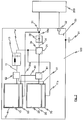
- Figure 1 shows a block diagram of a first exemplary embodiment of the oscillator 100 according to the invention for providing an oscillating voltage for a powder spray coating device 200, the powder spray coating device 200 having a high-voltage transformer (not represented) and a high-voltage cascade (likewise not represented).
- the primary winding of the high-voltage transformer is connected by way of schematically indicated supply lines between a first terminal 31 and a second terminal 32, at reference potential 33, of the oscillator 100.
- the oscillator 100 has a first signal generator 10 and a second signal generator 20.
- An intermediate circuit voltage 11 is generated by means of the first signal generator 10, a low-pass filter 13 being used for smoothing the intermediate circuit voltage 11, in particular whenever pulse-width modulation is used, so that at the output of this low-pass filter 13 there is a low-pass-filtered intermediate circuit voltage 11a, which is substantially a smoothed DC voltage.
- the second signal generator generates a modulation signal 21, which is generally likewise obtained by means of pulse-width modulation within the second signal generator 20.
- the modulation signal 21 is passed to the modulation input of a modulation unit 35 with a modulation signal isolating element 61 interposed.
- the low-pass-filtered intermediate circuit voltage 11a is likewise at the modulation unit 35 and is modulated with the modulation signal 21.
- the resultant oscillator voltage 34 is fed to a coupling capacitance 36, in order to eliminate the DC voltage component or DC offset thereof, and the capacitively coupled oscillator voltage 34a thus obtained is supplied to the first terminal 31 for outputting the oscillator voltage.
- the dropping voltage is picked off between the coupling capacitance 36 and the first terminal 31 and supplied to a first voltage monitoring device 60.
- This first voltage monitoring device 60 is designed for continuously measuring the thus picked-off oscillator voltage 34 or capacitively coupled oscillator voltage 34a and comparing it with a specified or specifiable oscillator voltage reference value.
- the first voltage monitoring device 60 outputs a modulation isolating signal 80 to the modulation signal isolating element 61, so that, given such a first comparison criterion, which corresponds to the case of a fault, the modulation signal isolating element interrupts the connection of the second signal generator 20 to the modulation unit 35.
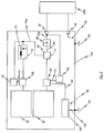
- An oscillator according to the invention as provided by the second exemplary embodiment, as shown in Figure 2 is constructed in a way similar to the first exemplary embodiment that can be seen in Figure 1 , but here an intermediate circuit voltage isolating element 62 is additionally provided in the path of the line between the first signal generator 10 and the low-pass filter 13. Of course, it is also possible to arrange this intermediate circuit voltage isolating element 62 only downstream of the low-pass filter.
- the second exemplary embodiment in Figure 2 provides a second voltage monitoring device 70, which picks off the intermediate circuit voltage 11, or in the exemplary embodiment represented the low-pass-filtered intermediate circuit voltage 11a, and continuously measures its value.
- the second voltage monitoring device 70 serves the purpose of comparing this continuously measured intermediate circuit voltage value with a specified or specifiable intermediate circuit voltage reference value and deriving from this comparison whether or not a second comparison criterion is given. If such a second comparison criterion is detected as satisfied, which corresponds to the case of a fault, an isolating signal (81) is output to the intermediate circuit voltage isolating element (62) connected to the second voltage monitoring device 70.
- the first processor unit 15 generates the intermediate circuit voltage 11, monitors the oscillator voltage 34 or 34a largely influenced by the second processor unit and, if a comparison criterion is satisfied, i.e. if it is detected that there is a fault, outputs a modulation isolating signal 80 to the modulation signal isolating element 61 in order to isolate the modulation signal 21 from the modulation unit 35.
- a corresponding integration of the second signal generator 20 and the second voltage monitoring device 70 in the second processor unit 25 achieves the effect that the intermediate circuit voltage 11 or 11a that is then monitored by the second processor unit 25 and is largely influenced by the first processor unit 15 is isolated from the modulation unit 35 by delivering an intermediate circuit voltage isolating signal 81 to the intermediate circuit voltage isolating element 62.
- the first processor unit 15 thereby monitors the voltage influenced by the second processor unit 25 and, conversely, the second processor unit 25 monitors the voltage generated by the first processor unit 15 and, as and when required, delivers a corresponding isolating command or an isolating signal. It is thereby ensured that, even in the case of failure of one of the two processor units 15, 25, the other one respectively ensures that the operational safety is improved.
- an earth current monitoring device 90 is provided in addition to the components represented in the second exemplary embodiment according to Figure 2 .
- the earth current monitoring device 90 has in this case an electrical connection both to the reference potential 32 and to a protective conductor or earth potential 91 and serves for measuring and monitoring during the coating operation by means of the powder spray coating device 200 current flowing via the powder cloud in the transfer of the powder particles to the earthed object to be coated (not represented). If the earth current monitoring device 90 establishes during the continuous measuring and comparison operation that a previously specified or specifiable maximum earth current is exceeded, the earth current monitoring device (90) is designed for delivering an earth current monitoring isolating signal (82).
- This earth current monitoring isolating signal (82) may be supplied to the modulation signal isolating element (61) alone, the intermediate circuit voltage isolating element (62) alone or both to the modulation signal isolating element (61) and to the intermediate circuit voltage isolating element (62). If it is therefore established by the earth current monitoring device (90) that such a specified or specifiable maximum earth current is exceeded, which corresponds to a fault, rapid potential isolation of the first terminal 31 for outputting an oscillator voltage 34 is achieved, which once again improves the operational safety of the oscillator according to the invention.
- the transistor isolating element 65 may, in particular, describe the structure of the modulation signal isolating element 61 and the intermediate circuit voltage isolating element 62.
- the transistor isolating element 65 according to Figure 5 consists here of a transistor driver 66 and a transistor 67, in the case represented a field-effect transistor.
- the transistor driver 66 has here an isolating signal terminal 68, which receives a logically inverted switch-off signal or shutdown signal. Further terminals (not represented in Figure 5 ), which serve for the modulation of the transistor input, that is to say in the example represented the gate terminal, are provided on the transistor driver 66.
Landscapes
- Electrostatic Spraying Apparatus (AREA)
Description
- The present invention relates to an oscillator for providing an oscillating voltage, the oscillating voltage being delivered to a powder spray coating device.
- It is known from the prior art to provide powder spraying devices, in particular spray guns and the like, for delivering a fluidized powder to an earthed surface to be coated with suitable high-voltage generators in order to impart high voltage to the coating powder that is leaving the powder spray coating device in the direction of the object to be coated.
- For this purpose, a transformer and a high-voltage cascade circuit connected thereto are provided, for example, within the powder spray coating device, the high-voltage transformer initially serving for the transformation to a moderately high voltage, and a voltage multiplication subsequently being performed in the sense of a cascade by the high-voltage cascade circuit supplied with the moderately high AC voltage, generally by combining diode paths and capacitors, for every half wave of the AC voltage.
- For this purpose, in the case of conventional oscillators an AC voltage is generated at their output, and is subsequently converted within the powder spray coating device by the interconnection of the high-voltage transformer and the cascade circuit into a high voltage that is subsequently intended to be imparted to the coating powder.
- In order to obtain an optimum coating result, in the case of conventional oscillators the amplitude of the AC voltage generated at their output is kept within certain limits as disclosed, e.g. in document
US 5,735,958 . However, it has been found that operational safety - in particular with regard to possibly required explosion protection - is not obtained here by, for example, the voltage being regulated in the conventional sense. In particular, in the case of conventional oscillators it is not ensured that, in the case of an event affecting operational safety, such as for example an abrupt or erroneous change in the oscillator voltage dropping across the high-voltage transformer of the powder spray coating device, that a voltage reduction to a safe value is possible in time. - On the basis of the problematic situation described, it is therefore the object of the present invention to develop an oscillator for providing an oscillating voltage for a powder spray coating device of the type mentioned at the beginning in such a way that operational safety is improved.
- This object is achieved in the case of an oscillator for providing an oscillating voltage for a powder spray coating device of the type mentioned at the beginning by the oscillator having a first signal generator for generating an intermediate circuit voltage and a second signal generator for generating a modulation signal as well as a modulation unit for generating an oscillator voltage, a first terminal for outputting the generated oscillator voltage to a powder spray coating device and a second terminal for returning this used oscillator voltage to a reference potential being provided, and a modulation signal isolating element, connected to the second signal generator, and a first voltage monitoring device also being provided. The modulation unit serves here for generating the oscillator voltage by modulation of the intermediate circuit voltage with the modulation signal. The first voltage monitoring device is designed here for continuously measuring the oscillator voltage, i.e. the voltage dropping across the terminals of the powder spray coating device during operation. At the same time, the first voltage monitoring device is designed for comparing the measured values thus obtained with at least one specified or specifiable oscillator voltage reference value. The first voltage monitoring device is also designed for checking the comparative values thus obtained as to whether a first comparison criterion is satisfied and, depending on whether this first comparison criterion is satisfied, outputting a modulation isolating signal to the modulation signal isolating element. The modulation signal isolating element is incorporated here in the connection of the second signal generator to the modulation unit and serves for interrupting the electrical connection between the second signal generator and the modulation unit in the presence of a modulation isolating signal.
- Satisfying the comparison criterion corresponds here to detecting the case of a fault, so that in such a case of a fault the modulation signal serving for the modulation is no longer fed to the modulation unit. The rapidly occurring switching off or isolation of the modulation signal from the modulation unit in the case of a fault means that, in such a case of a fault, there is then very quickly no longer any voltage at the first terminal of the oscillator according to the invention, as a result of which the operational safety improves significantly.
- Advantageous developments of the invention are specified in the subclaims.
- For example, it is provided that the oscillator has in addition to the modulation signal isolating element an intermediate circuit voltage isolating element, and that there is provided a second voltage monitoring device, which continuously measures the intermediate circuit voltage present at the modulation unit. In a similar way as in the case of the described interaction between the first voltage monitoring device and the modulation signal isolating element, the second voltage monitoring device serves here for comparing the continuously obtained measured value of the intermediate circuit voltage with an intermediate circuit voltage reference value, the intermediate circuit voltage reference value being specified or specifiable in advance. The comparison between the intermediate circuit voltage measured value and the intermediate circuit voltage reference value can be used to derive a second comparison criterion, satisfying which has the effect that an intermediate circuit voltage isolating signal is output to the intermediate circuit voltage isolating element. The intermediate circuit voltage isolating element is thereby switched into the signal path between the first signal generator and the modulation unit and is designed to isolate the first signal generator from the modulation unit when an intermediate circuit voltage isolating signal is present at a corresponding input of the intermediate circuit voltage isolating element.
- The second comparison criterion may in this case correspond in particular to a detected fault in the generation of the intermediate circuit voltage. In particular in the case when the first signal generator has a first pulse-width modulation unit, this pulse-width modulation serves for allowing the thus generated intermediate circuit voltage to be set or specified between a minimum value and a maximum value. This may be required in particular if the oscillator voltage, and consequently also the high voltage generated within the powder spray coating device, is to be limited to a certain value, for example in the case of the high voltage to 100 kV. Malfuntioning of the first signal generator, for example in the case of failure of the pulse-width modulation, may in such a case result in an excessively high intermediate circuit voltage, consequently also in an excessively high oscillator voltage, adversely affecting safety. Such a fault can be detected by the second voltage monitoring device in conjunction with the intermediate circuit voltage isolating element and be converted into a comparison criterion, whereby the intermediate circuit voltage isolating element isolates the modulation unit from the intermediate circuit voltage. The rapidly possible switching-off capability means that in such a case of a fault no voltage, or only a very minimal voltage, drops off between the first terminal and the second terminal, whereby the operational safety is further improved.
- It may also be provided that the at least one specified or specifiable oscillator voltage reference value is an oscillator voltage maximum value. The first comparison criterion would be satisfied here whenever the actually measured oscillator voltage exceeds this oscillator voltage maximum value, it being possible for the maximum value to be a maximum amplitude value, but also a maximum frequency value of the oscillator voltage.
- It may also be envisaged to provide in addition to the oscillator voltage maximum value, or exclusively as the oscillator voltage reference value, an oscillator voltage minimum value. Once again, the term "minimum value" in this connection means a lowering of the amplitude of the oscillator voltage and equally a possible lowering of the frequency of the oscillator voltage below a minimum value.
- In a similar way, an intermediate circuit voltage maximum value may be specified as an intermediate circuit voltage reference value, although a purely DC value generally exists as the intermediate circuit voltage, and consequently the second comparison criterion, which is determined by the second voltage monitoring device, is satisfied when the amplitude of the intermediate circuit voltage exceeds a maximum value.
- Consequently, it may similarly be envisaged to provide in addition to the intermediate circuit voltage maximum value, or exclusively as the intermediate circuit voltage reference value, an intermediate circuit voltage minimum value, the satisfying of the second comparison criterion once again relating to a falling of the amplitude of the intermediate circuit voltage below a minimum value.
- In an advantageous way, to ensure a switching-off operation that is as quick as possible, it may be envisaged to form the modulation signal isolating element, the intermediate circuit voltage isolating element or both the isolating elements mentioned as transistor isolating elements. Here it is particularly of advantage to provide fast-switching field-effect transistor isolating elements. The high switching speed here allows rapid switching off to be ensured, which further improves the operational safety.
- For a particularly effective and simple structure, it is provided in a particularly advantageous way that the transistor isolating element has a transistor driver and a transistor activated by means of the transistor driver. The use of a transistor driver, in particular and preferably a transistor driver block with a logical isolating signal terminal, allows the effect to be achieved here that switching off of the transistor can take place very quickly and easily when the transistor driver receives an isolating signal. In this case, the conduction of the transistor, that is in the case of a field-effect transistor the source-drain path, is interrupted. Particularly of advantage here is the use of a transistor driver block that has a logically inverted deactivation input. This means that such a driver allows operation of the transistor precisely when there is a signal at logical 1 ("high") at the logically inverted input, and then performs switching off when the signal at the input falls to logical 0 ("low"). This ensures that, in the case of failure of the voltage monitoring device assigned to the respective driver, that is to say the first or second voltage monitoring device, the transistor does not remain switched on or conducting, but instead switching off takes place (self-safety).
- In a particularly advantageous way, it may be envisaged to integrate the first signal generator and the first voltage monitoring device in a first processor unit. The first signal generator then also serves for generating the intermediate circuit voltage and the integrated first voltage monitoring device monitors the oscillator voltage. While saving a separate component for the first voltage monitoring device, the oscillator voltage is then monitored, with a second signal generator that is isolated from the first processor unit being checked by monitoring the oscillator voltage for malfunctioning, and the modulation signal isolating element that is connected to its output being switched off in the case of a fault.
- In addition to an integration of the first signal generator and the first voltage monitoring device in a first processor unit, or exclusively, it may be envisaged to integrate the second signal generator and the second voltage monitoring device in a second processor unit. The monitoring of the intermediate circuit voltage that is generated by the first signal generator with a second voltage monitoring device, integrated in the second processor unit, consequently makes possible - once again while saving a component - a monitoring of the intermediate circuit voltage that is generated independently of this second processor unit. In the case of detection of a fault, i.e. if the second comparison criterion is satisfied, the intermediate circuit voltage isolating element that is connected to the first signal generator is interrupted, and consequently the conduction of the intermediate circuit voltage to the modulation unit is isolated.
- In particular when an integration of the first signal generator and the first voltage monitoring device in a first processor unit and at the same time an integration of the second signal generator and the second voltage monitoring device in a second processor unit are used, relatively simple and effective mutual monitoring, that is in graphic terms "crosswise", is consequently possible, whereby the operational safety is again improved.
- It may additionally be provided that the oscillator also has an earth current monitoring device. Such an earth current monitoring device is connected both to the reference potential of the oscillator and to a protective conductor potential or earth potential, the object to be coated, to which coating powder is applied by means of the powder spray coating device, also being at earth potential. A charge carrier transfer via the powder cloud during spraying then produces an earth current flow between the reference potential of the oscillator and the earth potential. The earth current monitoring device is designed for continuously measuring this earth current and generating an earth current monitoring isolating signal if a previously specified or specifiable maximum earth current is exceeded. This earth current monitoring isolating signal is output to the modulation signal isolating element, to the intermediate circuit voltage isolating element or to both the isolating elements mentioned, so that, even when it is established that a maximum earth current is exceeded, a switching off that increases safety can take place irrespective of the behavior of the voltage profiles monitored by means of the first voltage monitoring device and the second voltage monitoring device.
- Finally, it may also be envisaged to couple the oscillator voltage capacitively to the first terminal for delivering the oscillator voltage.
- Four preferred exemplary embodiments of the oscillator according to the invention for providing an oscillating voltage for a powder spray coating device are explained in more detail below on the basis of a drawing, in which:
- Figure 1
- shows a block diagram of a first embodiment of the oscillator according to the invention with a first voltage monitoring device and a modulation signal isolating element;
- Figure 2
- shows an oscillator according to the invention in a second embodiment similar to the first embodiment in
Figure 1 , with additionally a second voltage monitoring device and an intermediate circuit voltage isolating element; - Figure 3
- shows an oscillator according to the invention as provided by a third embodiment, similar to the second exemplary embodiment in
Figure 2 , although here the voltage monitoring devices and the signal generators are respectively integrated in processor units; - Figure 4
- shows an oscillator according to the invention as provided by a fourth embodiment, similar to the second exemplary embodiment according to
Figure 2 , with an additional earth current monitoring device; and - Figure 5
- shows a transistor isolating element with a transistor driver and a field-effect transistor.
-
Figure 1 shows a block diagram of a first exemplary embodiment of theoscillator 100 according to the invention for providing an oscillating voltage for a powderspray coating device 200, the powderspray coating device 200 having a high-voltage transformer (not represented) and a high-voltage cascade (likewise not represented). The primary winding of the high-voltage transformer is connected by way of schematically indicated supply lines between afirst terminal 31 and asecond terminal 32, atreference potential 33, of theoscillator 100. - The
oscillator 100 has afirst signal generator 10 and asecond signal generator 20. Anintermediate circuit voltage 11 is generated by means of thefirst signal generator 10, a low-pass filter 13 being used for smoothing theintermediate circuit voltage 11, in particular whenever pulse-width modulation is used, so that at the output of this low-pass filter 13 there is a low-pass-filteredintermediate circuit voltage 11a, which is substantially a smoothed DC voltage. The second signal generator generates amodulation signal 21, which is generally likewise obtained by means of pulse-width modulation within thesecond signal generator 20. Themodulation signal 21 is passed to the modulation input of amodulation unit 35 with a modulationsignal isolating element 61 interposed. The low-pass-filteredintermediate circuit voltage 11a is likewise at themodulation unit 35 and is modulated with themodulation signal 21. Theresultant oscillator voltage 34 is fed to acoupling capacitance 36, in order to eliminate the DC voltage component or DC offset thereof, and the capacitively coupledoscillator voltage 34a thus obtained is supplied to thefirst terminal 31 for outputting the oscillator voltage. The dropping voltage is picked off between thecoupling capacitance 36 and thefirst terminal 31 and supplied to a firstvoltage monitoring device 60. This firstvoltage monitoring device 60 is designed for continuously measuring the thus picked-offoscillator voltage 34 or capacitively coupledoscillator voltage 34a and comparing it with a specified or specifiable oscillator voltage reference value. If a first comparison criterion is satisfied, the firstvoltage monitoring device 60 outputs amodulation isolating signal 80 to the modulationsignal isolating element 61, so that, given such a first comparison criterion, which corresponds to the case of a fault, the modulation signal isolating element interrupts the connection of thesecond signal generator 20 to themodulation unit 35. - The designations used in the exemplary embodiments described below represent elements that are the same or have the same effect with reference to the first exemplary embodiment according to
Figure 1 . - An oscillator according to the invention as provided by the second exemplary embodiment, as shown in
Figure 2 , is constructed in a way similar to the first exemplary embodiment that can be seen inFigure 1 , but here an intermediate circuitvoltage isolating element 62 is additionally provided in the path of the line between thefirst signal generator 10 and the low-pass filter 13. Of course, it is also possible to arrange this intermediate circuitvoltage isolating element 62 only downstream of the low-pass filter. Furthermore, the second exemplary embodiment inFigure 2 provides a secondvoltage monitoring device 70, which picks off theintermediate circuit voltage 11, or in the exemplary embodiment represented the low-pass-filteredintermediate circuit voltage 11a, and continuously measures its value. Furthermore, the secondvoltage monitoring device 70 serves the purpose of comparing this continuously measured intermediate circuit voltage value with a specified or specifiable intermediate circuit voltage reference value and deriving from this comparison whether or not a second comparison criterion is given. If such a second comparison criterion is detected as satisfied, which corresponds to the case of a fault, an isolating signal (81) is output to the intermediate circuit voltage isolating element (62) connected to the secondvoltage monitoring device 70. - As can be seen from
Figure 3 , it is envisaged according to a third exemplary embodiment not to provide the firstvoltage monitoring device 60 and the secondvoltage monitoring device 70 as separate components, but to integrate them together with the corresponding signal generators in processor units. Thus, thefirst signal generator 10 and the firstvoltage monitoring device 60 are combined in afirst processor unit 15; correspondingly, thesecond signal generator 20 and the secondvoltage monitoring device 70 are combined in asecond processor unit 25. By this arrangement according to the third exemplary embodiment, thefirst processor unit 15 generates theintermediate circuit voltage 11, monitors theoscillator voltage modulation isolating signal 80 to the modulationsignal isolating element 61 in order to isolate themodulation signal 21 from themodulation unit 35. - A corresponding integration of the
second signal generator 20 and the secondvoltage monitoring device 70 in thesecond processor unit 25 achieves the effect that theintermediate circuit voltage second processor unit 25 and is largely influenced by thefirst processor unit 15 is isolated from themodulation unit 35 by delivering an intermediate circuitvoltage isolating signal 81 to the intermediate circuitvoltage isolating element 62. - The
first processor unit 15 thereby monitors the voltage influenced by thesecond processor unit 25 and, conversely, thesecond processor unit 25 monitors the voltage generated by thefirst processor unit 15 and, as and when required, delivers a corresponding isolating command or an isolating signal. It is thereby ensured that, even in the case of failure of one of the twoprocessor units - In the fourth exemplary embodiment of the oscillator according to the invention, represented according to
Figure 4 , an earthcurrent monitoring device 90 is provided in addition to the components represented in the second exemplary embodiment according toFigure 2 . - The earth
current monitoring device 90 has in this case an electrical connection both to thereference potential 32 and to a protective conductor orearth potential 91 and serves for measuring and monitoring during the coating operation by means of the powderspray coating device 200 current flowing via the powder cloud in the transfer of the powder particles to the earthed object to be coated (not represented). If the earthcurrent monitoring device 90 establishes during the continuous measuring and comparison operation that a previously specified or specifiable maximum earth current is exceeded, the earth current monitoring device (90) is designed for delivering an earth current monitoring isolating signal (82). This earth current monitoring isolating signal (82) may be supplied to the modulation signal isolating element (61) alone, the intermediate circuit voltage isolating element (62) alone or both to the modulation signal isolating element (61) and to the intermediate circuit voltage isolating element (62). If it is therefore established by the earth current monitoring device (90) that such a specified or specifiable maximum earth current is exceeded, which corresponds to a fault, rapid potential isolation of thefirst terminal 31 for outputting anoscillator voltage 34 is achieved, which once again improves the operational safety of the oscillator according to the invention. - It is of course also possible, however, to integrate the earth
current monitoring device 90 at least partially in a possiblefirst processor unit 15 orsecond processor unit 25. - Finally, represented in
Figure 5 is atransistor isolating element 65, as can advantageously be used. Thetransistor isolating element 65 may, in particular, describe the structure of the modulationsignal isolating element 61 and the intermediate circuitvoltage isolating element 62. Thetransistor isolating element 65 according toFigure 5 consists here of atransistor driver 66 and atransistor 67, in the case represented a field-effect transistor. Thetransistor driver 66 has here an isolatingsignal terminal 68, which receives a logically inverted switch-off signal or shutdown signal. Further terminals (not represented inFigure 5 ), which serve for the modulation of the transistor input, that is to say in the example represented the gate terminal, are provided on thetransistor driver 66. - When the voltage at the isolating
signal terminal 68 drops to logical 0 ("low"), the conduction of thetransistor 67 is thereby interrupted. In the example represented according toFigure 5 , in the case of such atransistor isolating element 65 the present supply voltage VCC would no longer be switched through via the source-drain path, and consequently theintermediate circuit voltage 11 would be interrupted. - At this point it should be pointed out that all of the parts described above are claimed as essential to the invention in themselves alone and in any combination, in particular the details that are represented in the drawings. Modifications thereof are familiar to a person skilled in the art.
-
- 10
- first signal generator
- 11
- intermediate circuit voltage
- 11a
- low-pass-filtered intermediate circuit voltage
- 15
- first processor unit
- 20
- second signal generator
- 21
- modulation signal
- 25
- second processor unit
- 31
- first terminal for outputting an oscillator voltage
- 32
- second terminal for returning the used oscillator voltage to a reference potential
- 33
- reference potential
- 34
- oscillator voltage
- 34a
- capacitively coupled oscillator voltage
- 35
- modulation unit
- 36
- coupling capacitance
- 60
- first voltage monitoring device
- 61
- modulation signal isolating element
- 62
- intermediate circuit voltage isolating element
- 65
- transistor isolating element
- 66
- transistor driver
- 67
- transistor
- 68
- isolating signal terminal
- 70
- second voltage monitoring device
- 80
- modulation isolating signal
- 81
- intermediate circuit voltage isolating signal
- 82
- earth current monitoring isolating signal
- 90
- earth current monitoring device
- 91
- protective conductor potential
- 92
- earth current
- 100
- oscillator
- 200
- powder spray coating device
Claims (12)
- An oscillator (100) for providing an oscillating voltage for a powder spray coating device (200), the oscillator (100) having the following:- a first signal generator (10) for generating an intermediate circuit voltage (11);- a second signal generator (20) for generating a modulation signal (21);- a modulation unit (35) for generating an oscillator voltage (34);- a modulation signal isolating element (61), connected to the second signal generator (20), the modulation signal isolating element (61) being adapted to interrupt an electrical connection between the second signal generator (20) and the modulation unit (35) in the presence of a modulation isolating signal (80);- a first terminal (31) for outputting the oscillator voltage (34) to a powder spray coating device (200); and- a second terminal (32) for returning the used oscillator voltage (34) to a reference potential (33), in particular earth potential,the modulation unit (35) being designed for generating the oscillator voltage (34) by modulation of the intermediate circuit voltage (11) with the modulation signal (21), and a first voltage monitoring device (60) being provided, designed for continuously measuring the oscillator voltage (34), comparing it with at least one specified or specifiable oscillator voltage reference value and, if a first comparison criterion is satisfied, outputting the modulation isolating signal (80) to the modulation signal isolating element (61).
- The oscillator (100) as claimed in Claim 1, the oscillator (100) also having an intermediate circuit voltage isolating element (62), connected to the first signal generator (10), and a second voltage monitoring device (70) being provided, designed for continuously measuring the intermediate circuit voltage (11), comparing it with at least one specified or specifiable intermediate circuit voltage reference value and, if a second comparison criterion is satisfied, outputting an intermediate circuit voltage isolating signal (81) to the intermediate circuit voltage isolating element (62).
- The oscillator (100) as claimed in Claim 1 or 2, the at least one specified or specifiable oscillator voltage reference value being a maximum oscillator voltage value and the first comparison criterion being satisfied if the maximum oscillator voltage value is exceeded.
- The oscillator (100) as claimed in one of the preceding claims, the at least one specified or specifiable oscillator voltage reference value being a minimum oscillator voltage value and the first comparison criterion being satisfied if the minimum oscillator voltage value is not reached.
- The oscillator (100) as claimed in one of the preceding claims, the at least one specified or specifiable intermediate circuit voltage reference value being a maximum intermediate circuit voltage value and the second comparison criterion being satisfied if the maximum intermediate circuit voltage value is exceeded.
- The oscillator (100) as claimed in one of the preceding claims, the at least one specified or specifiable intermediate circuit voltage reference value being a minimum intermediate circuit voltage value and the second comparison criterion being satisfied if the minimum intermediate circuit voltage value is not reached.
- The oscillator (100) as claimed in one of the preceding claims, the modulation signal isolating element (61) and/or the intermediate circuit voltage isolating element (62) each being formed as a transistor isolating element (65), in particular as a fast-switching field-effect transistor isolating element.
- The oscillator (100) as claimed in Claim 7, the transistor isolating element (65) comprising a transistor driver (66), preferably a transistor driver (66) with a logical isolating signal terminal (68) and at least one transistor (67), in particular at least one field-effect transistor, and the transistor driver (66) being designed for isolating the conduction of the transistor (67) when an isolating signal is received.
- The oscillator (100) as claimed in one of the preceding claims, the first signal generator (10) and the first voltage monitoring device (60) being integrated in a first processor unit (15).
- The oscillator (100) as claimed in one of the preceding claims, the second signal generator (20) and the second voltage monitoring device (70) being integrated in a second processor unit (25).
- The oscillator (100) as claimed in one of the preceding claims, an earth current monitoring device (90) also being provided, designed for continuously measuring an earth current (92), in particular an earth current (92) between the reference potential (33) and a protective conductor potential (91), and outputting an earth current monitoring isolating signal (82) to the modulation signal isolating element and/or an earth current monitoring isolating signal (82) to the intermediate circuit voltage isolating element (62) if a previously specified or specifiable maximum earth current is exceeded.
- A method for providing an oscillating voltage provided at an oscillator (100) for a powder spray coating device (200), the oscillator (100) having the following:- a first signal generator (10) for generating an intermediate circuit voltage (11);- a second signal generator (20) for generating a modulation signal (21);- a modulation unit (35) for generating an oscillator voltage (34);- a modulation signal isolating element (61), connected to the second signal generator (20), the modulation signal isolating element (61) being adapted to interrupt an electrical connection between the second signal generator (20) and the modulation unit (35) in the presence of a modulation isolating signal (80);- a first terminal (31) for outputting the oscillator voltage (34) to a powder spray coating device (200); and- a second terminal (32) for returning the used oscillator voltage (34) to a reference potential (33), in particular earth potential,the modulation unit (35) generating the oscillator voltage (34) by modulation of the intermediate circuit voltage (11) with the modulation signal (21),
and a first voltage monitoring device (60) being provided, designed for performing the following method steps:- continuously measuring the oscillator voltage (34);- comparing the measured oscillator voltage (34) with at least one specified or specifiable oscillator voltage reference value;- establishing whether or not a first comparison criterion is satisfied;- if the first comparison criterion is satisfied: outputting the modulation isolating signal (80) to the modulation signal isolating element (61).
Applications Claiming Priority (2)
| Application Number | Priority Date | Filing Date | Title |
|---|---|---|---|
| DE102011004026A DE102011004026A1 (en) | 2011-02-14 | 2011-02-14 | Oscillator for a powder spray coating device |
| PCT/US2012/024836 WO2012112429A1 (en) | 2011-02-14 | 2012-02-13 | Oscillator for an electrostatic powder spray coating device |
Publications (2)
| Publication Number | Publication Date |
|---|---|
| EP2675572A1 EP2675572A1 (en) | 2013-12-25 |
| EP2675572B1 true EP2675572B1 (en) | 2016-04-27 |
Family
ID=45873211
Family Applications (1)
| Application Number | Title | Priority Date | Filing Date |
|---|---|---|---|
| EP12709987.7A Active EP2675572B1 (en) | 2011-02-14 | 2012-02-13 | Oscillator for an electrostatic powder spray coating device |
Country Status (4)
| Country | Link |
|---|---|
| US (1) | US9071192B2 (en) |
| EP (1) | EP2675572B1 (en) |
| DE (1) | DE102011004026A1 (en) |
| WO (1) | WO2012112429A1 (en) |
Family Cites Families (5)
| Publication number | Priority date | Publication date | Assignee | Title |
|---|---|---|---|---|
| GB1454395A (en) * | 1973-07-26 | 1976-11-03 | Volstatic Coatings Ltd | Power supply voltage control circuit |
| US4210858A (en) * | 1978-04-19 | 1980-07-01 | International Business Machines Corporation | High frequency high voltage power supply |
| DE4232026C2 (en) * | 1992-09-24 | 1996-10-24 | Wagner Int | Electrostatic coating gun and method for generating a high voltage |
| DE19511255A1 (en) * | 1995-03-27 | 1996-10-02 | Gema Volstatic Ag | Electrostatic spray coating device |
| CH713512B1 (en) * | 2006-09-05 | 2018-08-31 | Ms Oberflaechentechnik Ag | Method and apparatus for electrostatic coating. |
-
2011
- 2011-02-14 DE DE102011004026A patent/DE102011004026A1/en not_active Withdrawn
-
2012
- 2012-02-13 US US13/985,349 patent/US9071192B2/en active Active
- 2012-02-13 WO PCT/US2012/024836 patent/WO2012112429A1/en not_active Ceased
- 2012-02-13 EP EP12709987.7A patent/EP2675572B1/en active Active
Also Published As
| Publication number | Publication date |
|---|---|
| US9071192B2 (en) | 2015-06-30 |
| US20140055205A1 (en) | 2014-02-27 |
| EP2675572A1 (en) | 2013-12-25 |
| WO2012112429A1 (en) | 2012-08-23 |
| DE102011004026A1 (en) | 2012-08-16 |
Similar Documents
| Publication | Publication Date | Title |
|---|---|---|
| US9071051B2 (en) | Overvoltage protection unit with AC input current sensors | |
| TWI473414B (en) | Ac motor driving system | |
| EP3098952A2 (en) | Low capacitance drive with improved immunity | |
| US9188620B1 (en) | Method of detection and isolation of faults within power conversion and distribution systems | |
| US20120134185A1 (en) | Circuit for discharging ac power | |
| US6437462B1 (en) | Bi-directional DC/DC converter and control method therefor | |
| CN107534296A (en) | Bipolar DC electric power transmission structure | |
| JP6388758B2 (en) | Initial transient current suppression | |
| EP2880457A1 (en) | Twelve-pulse autotransformer rectifier units | |
| US20190280475A1 (en) | Method for eliminating an arc driven by means of at least one phase voltage source of a converter circuit | |
| US5991175A (en) | Control circuit for an in-rush current control element, and a protection circuit and power supply employing the same | |
| US9450507B2 (en) | Power supply apparatus with input voltage detection and method of operating the same | |
| JP2013162695A (en) | Device for controlling electric vehicle | |
| KR101611010B1 (en) | Pre-charging circuit of inverter | |
| US20140300303A1 (en) | Systems and methods for arc detecting and extinguishing in motors | |
| US20170054382A1 (en) | Control unit | |
| US9071192B2 (en) | Oscillator for a powder spray coating device | |
| CN207977738U (en) | The low-voltage direct distribution system in general-purpose aircraft distribution region | |
| US12519412B2 (en) | Common mode current feed fault protection | |
| US8941956B2 (en) | Switching ground tether circuit | |
| KR102029964B1 (en) | Apparatus for charging battery using induction current of gis enclosure | |
| US8659925B2 (en) | Three-level active rectification pulse width modulation control | |
| JP6534369B2 (en) | Ground fault detection device for voltage type inverter | |
| KR101540229B1 (en) | System for supplying impulse voltage | |
| JPWO2018078807A1 (en) | Power converter and harmonic suppression device |
Legal Events
| Date | Code | Title | Description |
|---|---|---|---|
| PUAI | Public reference made under article 153(3) epc to a published international application that has entered the european phase |
Free format text: ORIGINAL CODE: 0009012 |
|
| 17P | Request for examination filed |
Effective date: 20130909 |
|
| AK | Designated contracting states |
Kind code of ref document: A1 Designated state(s): AL AT BE BG CH CY CZ DE DK EE ES FI FR GB GR HR HU IE IS IT LI LT LU LV MC MK MT NL NO PL PT RO RS SE SI SK SM TR |
|
| DAX | Request for extension of the european patent (deleted) | ||
| REG | Reference to a national code |
Ref country code: DE Ref legal event code: R079 Ref document number: 602012017652 Country of ref document: DE Free format text: PREVIOUS MAIN CLASS: B05B0005100000 Ipc: B05B0005000000 |
|
| RIC1 | Information provided on ipc code assigned before grant |
Ipc: B05B 5/053 20060101ALI20150730BHEP Ipc: B05B 5/10 20060101ALI20150730BHEP Ipc: B05B 5/00 20060101AFI20150730BHEP Ipc: B05B 5/03 20060101ALI20150730BHEP |
|
| GRAP | Despatch of communication of intention to grant a patent |
Free format text: ORIGINAL CODE: EPIDOSNIGR1 |
|
| INTG | Intention to grant announced |
Effective date: 20151110 |
|
| GRAS | Grant fee paid |
Free format text: ORIGINAL CODE: EPIDOSNIGR3 |
|
| GRAA | (expected) grant |
Free format text: ORIGINAL CODE: 0009210 |
|
| AK | Designated contracting states |
Kind code of ref document: B1 Designated state(s): AL AT BE BG CH CY CZ DE DK EE ES FI FR GB GR HR HU IE IS IT LI LT LU LV MC MK MT NL NO PL PT RO RS SE SI SK SM TR |
|
| REG | Reference to a national code |
Ref country code: GB Ref legal event code: FG4D |
|
| REG | Reference to a national code |
Ref country code: CH Ref legal event code: EP |
|
| REG | Reference to a national code |
Ref country code: AT Ref legal event code: REF Ref document number: 794126 Country of ref document: AT Kind code of ref document: T Effective date: 20160515 |
|
| REG | Reference to a national code |
Ref country code: IE Ref legal event code: FG4D |
|
| REG | Reference to a national code |
Ref country code: DE Ref legal event code: R096 Ref document number: 602012017652 Country of ref document: DE |
|
| REG | Reference to a national code |
Ref country code: LT Ref legal event code: MG4D |
|
| REG | Reference to a national code |
Ref country code: NL Ref legal event code: MP Effective date: 20160427 |
|
| REG | Reference to a national code |
Ref country code: AT Ref legal event code: MK05 Ref document number: 794126 Country of ref document: AT Kind code of ref document: T Effective date: 20160427 |
|
| PG25 | Lapsed in a contracting state [announced via postgrant information from national office to epo] |
Ref country code: NL Free format text: LAPSE BECAUSE OF FAILURE TO SUBMIT A TRANSLATION OF THE DESCRIPTION OR TO PAY THE FEE WITHIN THE PRESCRIBED TIME-LIMIT Effective date: 20160427 |
|
| PG25 | Lapsed in a contracting state [announced via postgrant information from national office to epo] |
Ref country code: LT Free format text: LAPSE BECAUSE OF FAILURE TO SUBMIT A TRANSLATION OF THE DESCRIPTION OR TO PAY THE FEE WITHIN THE PRESCRIBED TIME-LIMIT Effective date: 20160427 Ref country code: PL Free format text: LAPSE BECAUSE OF FAILURE TO SUBMIT A TRANSLATION OF THE DESCRIPTION OR TO PAY THE FEE WITHIN THE PRESCRIBED TIME-LIMIT Effective date: 20160427 Ref country code: FI Free format text: LAPSE BECAUSE OF FAILURE TO SUBMIT A TRANSLATION OF THE DESCRIPTION OR TO PAY THE FEE WITHIN THE PRESCRIBED TIME-LIMIT Effective date: 20160427 Ref country code: NO Free format text: LAPSE BECAUSE OF FAILURE TO SUBMIT A TRANSLATION OF THE DESCRIPTION OR TO PAY THE FEE WITHIN THE PRESCRIBED TIME-LIMIT Effective date: 20160727 |
|
| PG25 | Lapsed in a contracting state [announced via postgrant information from national office to epo] |
Ref country code: RS Free format text: LAPSE BECAUSE OF FAILURE TO SUBMIT A TRANSLATION OF THE DESCRIPTION OR TO PAY THE FEE WITHIN THE PRESCRIBED TIME-LIMIT Effective date: 20160427 Ref country code: LV Free format text: LAPSE BECAUSE OF FAILURE TO SUBMIT A TRANSLATION OF THE DESCRIPTION OR TO PAY THE FEE WITHIN THE PRESCRIBED TIME-LIMIT Effective date: 20160427 Ref country code: GR Free format text: LAPSE BECAUSE OF FAILURE TO SUBMIT A TRANSLATION OF THE DESCRIPTION OR TO PAY THE FEE WITHIN THE PRESCRIBED TIME-LIMIT Effective date: 20160728 Ref country code: HR Free format text: LAPSE BECAUSE OF FAILURE TO SUBMIT A TRANSLATION OF THE DESCRIPTION OR TO PAY THE FEE WITHIN THE PRESCRIBED TIME-LIMIT Effective date: 20160427 Ref country code: AT Free format text: LAPSE BECAUSE OF FAILURE TO SUBMIT A TRANSLATION OF THE DESCRIPTION OR TO PAY THE FEE WITHIN THE PRESCRIBED TIME-LIMIT Effective date: 20160427 Ref country code: SE Free format text: LAPSE BECAUSE OF FAILURE TO SUBMIT A TRANSLATION OF THE DESCRIPTION OR TO PAY THE FEE WITHIN THE PRESCRIBED TIME-LIMIT Effective date: 20160427 Ref country code: ES Free format text: LAPSE BECAUSE OF FAILURE TO SUBMIT A TRANSLATION OF THE DESCRIPTION OR TO PAY THE FEE WITHIN THE PRESCRIBED TIME-LIMIT Effective date: 20160427 Ref country code: PT Free format text: LAPSE BECAUSE OF FAILURE TO SUBMIT A TRANSLATION OF THE DESCRIPTION OR TO PAY THE FEE WITHIN THE PRESCRIBED TIME-LIMIT Effective date: 20160829 |
|
| PG25 | Lapsed in a contracting state [announced via postgrant information from national office to epo] |
Ref country code: BE Free format text: LAPSE BECAUSE OF FAILURE TO SUBMIT A TRANSLATION OF THE DESCRIPTION OR TO PAY THE FEE WITHIN THE PRESCRIBED TIME-LIMIT Effective date: 20160427 |
|
| REG | Reference to a national code |
Ref country code: DE Ref legal event code: R097 Ref document number: 602012017652 Country of ref document: DE |
|
| PG25 | Lapsed in a contracting state [announced via postgrant information from national office to epo] |
Ref country code: CZ Free format text: LAPSE BECAUSE OF FAILURE TO SUBMIT A TRANSLATION OF THE DESCRIPTION OR TO PAY THE FEE WITHIN THE PRESCRIBED TIME-LIMIT Effective date: 20160427 Ref country code: DK Free format text: LAPSE BECAUSE OF FAILURE TO SUBMIT A TRANSLATION OF THE DESCRIPTION OR TO PAY THE FEE WITHIN THE PRESCRIBED TIME-LIMIT Effective date: 20160427 Ref country code: SK Free format text: LAPSE BECAUSE OF FAILURE TO SUBMIT A TRANSLATION OF THE DESCRIPTION OR TO PAY THE FEE WITHIN THE PRESCRIBED TIME-LIMIT Effective date: 20160427 Ref country code: EE Free format text: LAPSE BECAUSE OF FAILURE TO SUBMIT A TRANSLATION OF THE DESCRIPTION OR TO PAY THE FEE WITHIN THE PRESCRIBED TIME-LIMIT Effective date: 20160427 Ref country code: RO Free format text: LAPSE BECAUSE OF FAILURE TO SUBMIT A TRANSLATION OF THE DESCRIPTION OR TO PAY THE FEE WITHIN THE PRESCRIBED TIME-LIMIT Effective date: 20160427 |
|
| REG | Reference to a national code |
Ref country code: FR Ref legal event code: PLFP Year of fee payment: 6 |
|
| PG25 | Lapsed in a contracting state [announced via postgrant information from national office to epo] |
Ref country code: SM Free format text: LAPSE BECAUSE OF FAILURE TO SUBMIT A TRANSLATION OF THE DESCRIPTION OR TO PAY THE FEE WITHIN THE PRESCRIBED TIME-LIMIT Effective date: 20160427 |
|
| PLBE | No opposition filed within time limit |
Free format text: ORIGINAL CODE: 0009261 |
|
| STAA | Information on the status of an ep patent application or granted ep patent |
Free format text: STATUS: NO OPPOSITION FILED WITHIN TIME LIMIT |
|
| 26N | No opposition filed |
Effective date: 20170130 |
|
| PG25 | Lapsed in a contracting state [announced via postgrant information from national office to epo] |
Ref country code: SI Free format text: LAPSE BECAUSE OF FAILURE TO SUBMIT A TRANSLATION OF THE DESCRIPTION OR TO PAY THE FEE WITHIN THE PRESCRIBED TIME-LIMIT Effective date: 20160427 |
|
| PG25 | Lapsed in a contracting state [announced via postgrant information from national office to epo] |
Ref country code: MC Free format text: LAPSE BECAUSE OF FAILURE TO SUBMIT A TRANSLATION OF THE DESCRIPTION OR TO PAY THE FEE WITHIN THE PRESCRIBED TIME-LIMIT Effective date: 20160427 |
|
| REG | Reference to a national code |
Ref country code: IE Ref legal event code: MM4A |
|
| PG25 | Lapsed in a contracting state [announced via postgrant information from national office to epo] |
Ref country code: LU Free format text: LAPSE BECAUSE OF NON-PAYMENT OF DUE FEES Effective date: 20170213 |
|
| REG | Reference to a national code |
Ref country code: FR Ref legal event code: PLFP Year of fee payment: 7 |
|
| PG25 | Lapsed in a contracting state [announced via postgrant information from national office to epo] |
Ref country code: IE Free format text: LAPSE BECAUSE OF NON-PAYMENT OF DUE FEES Effective date: 20170213 |
|
| PG25 | Lapsed in a contracting state [announced via postgrant information from national office to epo] |
Ref country code: MT Free format text: LAPSE BECAUSE OF NON-PAYMENT OF DUE FEES Effective date: 20170213 |
|
| PG25 | Lapsed in a contracting state [announced via postgrant information from national office to epo] |
Ref country code: AL Free format text: LAPSE BECAUSE OF FAILURE TO SUBMIT A TRANSLATION OF THE DESCRIPTION OR TO PAY THE FEE WITHIN THE PRESCRIBED TIME-LIMIT Effective date: 20160427 |
|
| PG25 | Lapsed in a contracting state [announced via postgrant information from national office to epo] |
Ref country code: HU Free format text: LAPSE BECAUSE OF FAILURE TO SUBMIT A TRANSLATION OF THE DESCRIPTION OR TO PAY THE FEE WITHIN THE PRESCRIBED TIME-LIMIT; INVALID AB INITIO Effective date: 20120213 |
|
| PG25 | Lapsed in a contracting state [announced via postgrant information from national office to epo] |
Ref country code: BG Free format text: LAPSE BECAUSE OF FAILURE TO SUBMIT A TRANSLATION OF THE DESCRIPTION OR TO PAY THE FEE WITHIN THE PRESCRIBED TIME-LIMIT Effective date: 20160427 |
|
| PG25 | Lapsed in a contracting state [announced via postgrant information from national office to epo] |
Ref country code: CY Free format text: LAPSE BECAUSE OF NON-PAYMENT OF DUE FEES Effective date: 20160427 |
|
| PG25 | Lapsed in a contracting state [announced via postgrant information from national office to epo] |
Ref country code: MK Free format text: LAPSE BECAUSE OF FAILURE TO SUBMIT A TRANSLATION OF THE DESCRIPTION OR TO PAY THE FEE WITHIN THE PRESCRIBED TIME-LIMIT Effective date: 20160427 |
|
| PG25 | Lapsed in a contracting state [announced via postgrant information from national office to epo] |
Ref country code: IS Free format text: LAPSE BECAUSE OF FAILURE TO SUBMIT A TRANSLATION OF THE DESCRIPTION OR TO PAY THE FEE WITHIN THE PRESCRIBED TIME-LIMIT Effective date: 20160827 |
|
| P01 | Opt-out of the competence of the unified patent court (upc) registered |
Effective date: 20230621 |
|
| REG | Reference to a national code |
Ref country code: DE Ref legal event code: R081 Ref document number: 602012017652 Country of ref document: DE Owner name: GEMA SWITZERLAND GMBH, CH Free format text: FORMER OWNER: GEMA SWITZERLAND GMBH, ST. GALLEN, CH |
|
| REG | Reference to a national code |
Ref country code: CH Ref legal event code: U11 Free format text: ST27 STATUS EVENT CODE: U-0-0-U10-U11 (AS PROVIDED BY THE NATIONAL OFFICE) Effective date: 20260301 |
|
| PGFP | Annual fee paid to national office [announced via postgrant information from national office to epo] |
Ref country code: GB Payment date: 20260227 Year of fee payment: 15 |
|
| PGFP | Annual fee paid to national office [announced via postgrant information from national office to epo] |
Ref country code: DE Payment date: 20260227 Year of fee payment: 15 |
|
| PGFP | Annual fee paid to national office [announced via postgrant information from national office to epo] |
Ref country code: IT Payment date: 20260219 Year of fee payment: 15 |
|
| PGFP | Annual fee paid to national office [announced via postgrant information from national office to epo] |
Ref country code: FR Payment date: 20260225 Year of fee payment: 15 |
|
| PGFP | Annual fee paid to national office [announced via postgrant information from national office to epo] |
Ref country code: TR Payment date: 20260127 Year of fee payment: 15 |
|
| PGFP | Annual fee paid to national office [announced via postgrant information from national office to epo] |
Ref country code: CH Payment date: 20260301 Year of fee payment: 15 |