EP2674970A2 - Integrated circuit build-up package and method of manufacturing the same with adhesive die mounting to a dielectric layer - Google Patents
Integrated circuit build-up package and method of manufacturing the same with adhesive die mounting to a dielectric layer Download PDFInfo
- Publication number
- EP2674970A2 EP2674970A2 EP20130171914 EP13171914A EP2674970A2 EP 2674970 A2 EP2674970 A2 EP 2674970A2 EP 20130171914 EP20130171914 EP 20130171914 EP 13171914 A EP13171914 A EP 13171914A EP 2674970 A2 EP2674970 A2 EP 2674970A2
- Authority
- EP
- European Patent Office
- Prior art keywords
- die
- adhesive layer
- layer
- adhesive
- dielectric layer
- Prior art date
- Legal status (The legal status is an assumption and is not a legal conclusion. Google has not performed a legal analysis and makes no representation as to the accuracy of the status listed.)
- Ceased
Links
Images






Classifications
-
- H—ELECTRICITY
- H10—SEMICONDUCTOR DEVICES; ELECTRIC SOLID-STATE DEVICES NOT OTHERWISE PROVIDED FOR
- H10W—GENERIC PACKAGES, INTERCONNECTIONS, CONNECTORS OR OTHER CONSTRUCTIONAL DETAILS OF DEVICES COVERED BY CLASS H10
- H10W90/00—Package configurations
-
- H—ELECTRICITY
- H10—SEMICONDUCTOR DEVICES; ELECTRIC SOLID-STATE DEVICES NOT OTHERWISE PROVIDED FOR
- H10W—GENERIC PACKAGES, INTERCONNECTIONS, CONNECTORS OR OTHER CONSTRUCTIONAL DETAILS OF DEVICES COVERED BY CLASS H10
- H10W42/00—Arrangements for protection of devices
-
- H—ELECTRICITY
- H10—SEMICONDUCTOR DEVICES; ELECTRIC SOLID-STATE DEVICES NOT OTHERWISE PROVIDED FOR
- H10P—GENERIC PROCESSES OR APPARATUS FOR THE MANUFACTURE OR TREATMENT OF DEVICES COVERED BY CLASS H10
- H10P72/00—Handling or holding of wafers, substrates or devices during manufacture or treatment thereof
- H10P72/70—Handling or holding of wafers, substrates or devices during manufacture or treatment thereof for supporting or gripping
- H10P72/74—Handling or holding of wafers, substrates or devices during manufacture or treatment thereof for supporting or gripping using temporarily an auxiliary support
- H10P72/7402—Wafer tapes, e.g. grinding or dicing support tapes
-
- H—ELECTRICITY
- H10—SEMICONDUCTOR DEVICES; ELECTRIC SOLID-STATE DEVICES NOT OTHERWISE PROVIDED FOR
- H10W—GENERIC PACKAGES, INTERCONNECTIONS, CONNECTORS OR OTHER CONSTRUCTIONAL DETAILS OF DEVICES COVERED BY CLASS H10
- H10W70/00—Package substrates; Interposers; Redistribution layers [RDL]
- H10W70/01—Manufacture or treatment
- H10W70/05—Manufacture or treatment of insulating or insulated package substrates, or of interposers, or of redistribution layers
-
- H—ELECTRICITY
- H10—SEMICONDUCTOR DEVICES; ELECTRIC SOLID-STATE DEVICES NOT OTHERWISE PROVIDED FOR
- H10W—GENERIC PACKAGES, INTERCONNECTIONS, CONNECTORS OR OTHER CONSTRUCTIONAL DETAILS OF DEVICES COVERED BY CLASS H10
- H10W70/00—Package substrates; Interposers; Redistribution layers [RDL]
- H10W70/01—Manufacture or treatment
- H10W70/05—Manufacture or treatment of insulating or insulated package substrates, or of interposers, or of redistribution layers
- H10W70/08—Manufacture or treatment of insulating or insulated package substrates, or of interposers, or of redistribution layers by depositing layers on the chip or wafer, e.g. "chip-first" RDLs
- H10W70/09—Manufacture or treatment of insulating or insulated package substrates, or of interposers, or of redistribution layers by depositing layers on the chip or wafer, e.g. "chip-first" RDLs extending onto an encapsulation that laterally surrounds the chip or wafer, e.g. fan-out wafer level package [FOWLP] RDLs
-
- H—ELECTRICITY
- H10—SEMICONDUCTOR DEVICES; ELECTRIC SOLID-STATE DEVICES NOT OTHERWISE PROVIDED FOR
- H10W—GENERIC PACKAGES, INTERCONNECTIONS, CONNECTORS OR OTHER CONSTRUCTIONAL DETAILS OF DEVICES COVERED BY CLASS H10
- H10W70/00—Package substrates; Interposers; Redistribution layers [RDL]
- H10W70/01—Manufacture or treatment
- H10W70/05—Manufacture or treatment of insulating or insulated package substrates, or of interposers, or of redistribution layers
- H10W70/095—Manufacture or treatment of insulating or insulated package substrates, or of interposers, or of redistribution layers of vias therein
-
- H—ELECTRICITY
- H10—SEMICONDUCTOR DEVICES; ELECTRIC SOLID-STATE DEVICES NOT OTHERWISE PROVIDED FOR
- H10W—GENERIC PACKAGES, INTERCONNECTIONS, CONNECTORS OR OTHER CONSTRUCTIONAL DETAILS OF DEVICES COVERED BY CLASS H10
- H10W70/00—Package substrates; Interposers; Redistribution layers [RDL]
- H10W70/60—Insulating or insulated package substrates; Interposers; Redistribution layers
-
- H—ELECTRICITY
- H10—SEMICONDUCTOR DEVICES; ELECTRIC SOLID-STATE DEVICES NOT OTHERWISE PROVIDED FOR
- H10W—GENERIC PACKAGES, INTERCONNECTIONS, CONNECTORS OR OTHER CONSTRUCTIONAL DETAILS OF DEVICES COVERED BY CLASS H10
- H10W70/00—Package substrates; Interposers; Redistribution layers [RDL]
- H10W70/60—Insulating or insulated package substrates; Interposers; Redistribution layers
- H10W70/611—Insulating or insulated package substrates; Interposers; Redistribution layers for connecting multiple chips together
-
- H—ELECTRICITY
- H10—SEMICONDUCTOR DEVICES; ELECTRIC SOLID-STATE DEVICES NOT OTHERWISE PROVIDED FOR
- H10W—GENERIC PACKAGES, INTERCONNECTIONS, CONNECTORS OR OTHER CONSTRUCTIONAL DETAILS OF DEVICES COVERED BY CLASS H10
- H10W70/00—Package substrates; Interposers; Redistribution layers [RDL]
- H10W70/60—Insulating or insulated package substrates; Interposers; Redistribution layers
- H10W70/62—Insulating or insulated package substrates; Interposers; Redistribution layers characterised by their interconnections
- H10W70/63—Vias, e.g. via plugs
- H10W70/635—Through-vias
-
- H—ELECTRICITY
- H10—SEMICONDUCTOR DEVICES; ELECTRIC SOLID-STATE DEVICES NOT OTHERWISE PROVIDED FOR
- H10W—GENERIC PACKAGES, INTERCONNECTIONS, CONNECTORS OR OTHER CONSTRUCTIONAL DETAILS OF DEVICES COVERED BY CLASS H10
- H10W70/00—Package substrates; Interposers; Redistribution layers [RDL]
- H10W70/60—Insulating or insulated package substrates; Interposers; Redistribution layers
- H10W70/62—Insulating or insulated package substrates; Interposers; Redistribution layers characterised by their interconnections
- H10W70/65—Shapes or dispositions of interconnections
-
- H—ELECTRICITY
- H10—SEMICONDUCTOR DEVICES; ELECTRIC SOLID-STATE DEVICES NOT OTHERWISE PROVIDED FOR
- H10W—GENERIC PACKAGES, INTERCONNECTIONS, CONNECTORS OR OTHER CONSTRUCTIONAL DETAILS OF DEVICES COVERED BY CLASS H10
- H10W70/00—Package substrates; Interposers; Redistribution layers [RDL]
- H10W70/60—Insulating or insulated package substrates; Interposers; Redistribution layers
- H10W70/67—Insulating or insulated package substrates; Interposers; Redistribution layers characterised by their insulating layers or insulating parts
- H10W70/68—Shapes or dispositions thereof
- H10W70/685—Shapes or dispositions thereof comprising multiple insulating layers
-
- H—ELECTRICITY
- H10—SEMICONDUCTOR DEVICES; ELECTRIC SOLID-STATE DEVICES NOT OTHERWISE PROVIDED FOR
- H10W—GENERIC PACKAGES, INTERCONNECTIONS, CONNECTORS OR OTHER CONSTRUCTIONAL DETAILS OF DEVICES COVERED BY CLASS H10
- H10W72/00—Interconnections or connectors in packages
- H10W72/30—Die-attach connectors
-
- H—ELECTRICITY
- H05—ELECTRIC TECHNIQUES NOT OTHERWISE PROVIDED FOR
- H05K—PRINTED CIRCUITS; CASINGS OR CONSTRUCTIONAL DETAILS OF ELECTRIC APPARATUS; MANUFACTURE OF ASSEMBLAGES OF ELECTRICAL COMPONENTS
- H05K3/00—Apparatus or processes for manufacturing printed circuits
- H05K3/30—Assembling printed circuits with electric components, e.g. with resistors
- H05K3/303—Assembling printed circuits with electric components, e.g. with resistors with surface mounted components
- H05K3/305—Affixing by adhesive
-
- H—ELECTRICITY
- H10—SEMICONDUCTOR DEVICES; ELECTRIC SOLID-STATE DEVICES NOT OTHERWISE PROVIDED FOR
- H10P—GENERIC PROCESSES OR APPARATUS FOR THE MANUFACTURE OR TREATMENT OF DEVICES COVERED BY CLASS H10
- H10P72/00—Handling or holding of wafers, substrates or devices during manufacture or treatment thereof
- H10P72/70—Handling or holding of wafers, substrates or devices during manufacture or treatment thereof for supporting or gripping
- H10P72/74—Handling or holding of wafers, substrates or devices during manufacture or treatment thereof for supporting or gripping using temporarily an auxiliary support
- H10P72/7416—Handling or holding of wafers, substrates or devices during manufacture or treatment thereof for supporting or gripping using temporarily an auxiliary support used during dicing or grinding
-
- H—ELECTRICITY
- H10—SEMICONDUCTOR DEVICES; ELECTRIC SOLID-STATE DEVICES NOT OTHERWISE PROVIDED FOR
- H10P—GENERIC PROCESSES OR APPARATUS FOR THE MANUFACTURE OR TREATMENT OF DEVICES COVERED BY CLASS H10
- H10P72/00—Handling or holding of wafers, substrates or devices during manufacture or treatment thereof
- H10P72/70—Handling or holding of wafers, substrates or devices during manufacture or treatment thereof for supporting or gripping
- H10P72/74—Handling or holding of wafers, substrates or devices during manufacture or treatment thereof for supporting or gripping using temporarily an auxiliary support
- H10P72/7422—Handling or holding of wafers, substrates or devices during manufacture or treatment thereof for supporting or gripping using temporarily an auxiliary support used to protect an active side of a device or wafer
-
- H—ELECTRICITY
- H10—SEMICONDUCTOR DEVICES; ELECTRIC SOLID-STATE DEVICES NOT OTHERWISE PROVIDED FOR
- H10P—GENERIC PROCESSES OR APPARATUS FOR THE MANUFACTURE OR TREATMENT OF DEVICES COVERED BY CLASS H10
- H10P72/00—Handling or holding of wafers, substrates or devices during manufacture or treatment thereof
- H10P72/70—Handling or holding of wafers, substrates or devices during manufacture or treatment thereof for supporting or gripping
- H10P72/74—Handling or holding of wafers, substrates or devices during manufacture or treatment thereof for supporting or gripping using temporarily an auxiliary support
- H10P72/744—Details of chemical or physical process used for separating the auxiliary support from a device or a wafer
-
- H—ELECTRICITY
- H10—SEMICONDUCTOR DEVICES; ELECTRIC SOLID-STATE DEVICES NOT OTHERWISE PROVIDED FOR
- H10W—GENERIC PACKAGES, INTERCONNECTIONS, CONNECTORS OR OTHER CONSTRUCTIONAL DETAILS OF DEVICES COVERED BY CLASS H10
- H10W70/00—Package substrates; Interposers; Redistribution layers [RDL]
- H10W70/01—Manufacture or treatment
- H10W70/05—Manufacture or treatment of insulating or insulated package substrates, or of interposers, or of redistribution layers
- H10W70/093—Connecting or disconnecting other interconnections thereto or therefrom, e.g. connecting bond wires or bumps
-
- H—ELECTRICITY
- H10—SEMICONDUCTOR DEVICES; ELECTRIC SOLID-STATE DEVICES NOT OTHERWISE PROVIDED FOR
- H10W—GENERIC PACKAGES, INTERCONNECTIONS, CONNECTORS OR OTHER CONSTRUCTIONAL DETAILS OF DEVICES COVERED BY CLASS H10
- H10W72/00—Interconnections or connectors in packages
- H10W72/01—Manufacture or treatment
- H10W72/013—Manufacture or treatment of die-attach connectors
- H10W72/01304—Manufacture or treatment of die-attach connectors using temporary auxiliary members, e.g. using sacrificial coatings or handle substrates
-
- H—ELECTRICITY
- H10—SEMICONDUCTOR DEVICES; ELECTRIC SOLID-STATE DEVICES NOT OTHERWISE PROVIDED FOR
- H10W—GENERIC PACKAGES, INTERCONNECTIONS, CONNECTORS OR OTHER CONSTRUCTIONAL DETAILS OF DEVICES COVERED BY CLASS H10
- H10W72/00—Interconnections or connectors in packages
- H10W72/01—Manufacture or treatment
- H10W72/013—Manufacture or treatment of die-attach connectors
- H10W72/01321—Manufacture or treatment of die-attach connectors using local deposition
- H10W72/01323—Manufacture or treatment of die-attach connectors using local deposition in liquid form, e.g. by dispensing droplets or by screen printing
-
- H—ELECTRICITY
- H10—SEMICONDUCTOR DEVICES; ELECTRIC SOLID-STATE DEVICES NOT OTHERWISE PROVIDED FOR
- H10W—GENERIC PACKAGES, INTERCONNECTIONS, CONNECTORS OR OTHER CONSTRUCTIONAL DETAILS OF DEVICES COVERED BY CLASS H10
- H10W72/00—Interconnections or connectors in packages
- H10W72/01—Manufacture or treatment
- H10W72/013—Manufacture or treatment of die-attach connectors
- H10W72/01331—Manufacture or treatment of die-attach connectors using blanket deposition
- H10W72/01333—Manufacture or treatment of die-attach connectors using blanket deposition in liquid form, e.g. spin coating, spray coating or immersion coating
-
- H—ELECTRICITY
- H10—SEMICONDUCTOR DEVICES; ELECTRIC SOLID-STATE DEVICES NOT OTHERWISE PROVIDED FOR
- H10W—GENERIC PACKAGES, INTERCONNECTIONS, CONNECTORS OR OTHER CONSTRUCTIONAL DETAILS OF DEVICES COVERED BY CLASS H10
- H10W72/00—Interconnections or connectors in packages
- H10W72/01—Manufacture or treatment
- H10W72/013—Manufacture or treatment of die-attach connectors
- H10W72/01331—Manufacture or treatment of die-attach connectors using blanket deposition
- H10W72/01336—Manufacture or treatment of die-attach connectors using blanket deposition in solid form, e.g. by using a powder or by laminating a foil
-
- H—ELECTRICITY
- H10—SEMICONDUCTOR DEVICES; ELECTRIC SOLID-STATE DEVICES NOT OTHERWISE PROVIDED FOR
- H10W—GENERIC PACKAGES, INTERCONNECTIONS, CONNECTORS OR OTHER CONSTRUCTIONAL DETAILS OF DEVICES COVERED BY CLASS H10
- H10W72/00—Interconnections or connectors in packages
- H10W72/01—Manufacture or treatment
- H10W72/013—Manufacture or treatment of die-attach connectors
- H10W72/01365—Thermally treating
-
- H—ELECTRICITY
- H10—SEMICONDUCTOR DEVICES; ELECTRIC SOLID-STATE DEVICES NOT OTHERWISE PROVIDED FOR
- H10W—GENERIC PACKAGES, INTERCONNECTIONS, CONNECTORS OR OTHER CONSTRUCTIONAL DETAILS OF DEVICES COVERED BY CLASS H10
- H10W72/00—Interconnections or connectors in packages
- H10W72/01—Manufacture or treatment
- H10W72/013—Manufacture or treatment of die-attach connectors
- H10W72/01371—Cleaning, e.g. oxide removal or de-smearing
-
- H—ELECTRICITY
- H10—SEMICONDUCTOR DEVICES; ELECTRIC SOLID-STATE DEVICES NOT OTHERWISE PROVIDED FOR
- H10W—GENERIC PACKAGES, INTERCONNECTIONS, CONNECTORS OR OTHER CONSTRUCTIONAL DETAILS OF DEVICES COVERED BY CLASS H10
- H10W72/00—Interconnections or connectors in packages
- H10W72/01—Manufacture or treatment
- H10W72/0198—Manufacture or treatment batch processes
-
- H—ELECTRICITY
- H10—SEMICONDUCTOR DEVICES; ELECTRIC SOLID-STATE DEVICES NOT OTHERWISE PROVIDED FOR
- H10W—GENERIC PACKAGES, INTERCONNECTIONS, CONNECTORS OR OTHER CONSTRUCTIONAL DETAILS OF DEVICES COVERED BY CLASS H10
- H10W72/00—Interconnections or connectors in packages
- H10W72/071—Connecting or disconnecting
- H10W72/073—Connecting or disconnecting of die-attach connectors
-
- H—ELECTRICITY
- H10—SEMICONDUCTOR DEVICES; ELECTRIC SOLID-STATE DEVICES NOT OTHERWISE PROVIDED FOR
- H10W—GENERIC PACKAGES, INTERCONNECTIONS, CONNECTORS OR OTHER CONSTRUCTIONAL DETAILS OF DEVICES COVERED BY CLASS H10
- H10W72/00—Interconnections or connectors in packages
- H10W72/071—Connecting or disconnecting
- H10W72/073—Connecting or disconnecting of die-attach connectors
- H10W72/07331—Connecting techniques
- H10W72/07337—Connecting techniques using a polymer adhesive, e.g. an adhesive based on silicone or epoxy
- H10W72/07338—Connecting techniques using a polymer adhesive, e.g. an adhesive based on silicone or epoxy hardening the adhesive by curing, e.g. thermosetting
-
- H—ELECTRICITY
- H10—SEMICONDUCTOR DEVICES; ELECTRIC SOLID-STATE DEVICES NOT OTHERWISE PROVIDED FOR
- H10W—GENERIC PACKAGES, INTERCONNECTIONS, CONNECTORS OR OTHER CONSTRUCTIONAL DETAILS OF DEVICES COVERED BY CLASS H10
- H10W72/00—Interconnections or connectors in packages
- H10W72/30—Die-attach connectors
- H10W72/351—Materials of die-attach connectors
- H10W72/353—Materials of die-attach connectors not comprising solid metals or solid metalloids, e.g. ceramics
- H10W72/354—Materials of die-attach connectors not comprising solid metals or solid metalloids, e.g. ceramics comprising polymers
-
- H—ELECTRICITY
- H10—SEMICONDUCTOR DEVICES; ELECTRIC SOLID-STATE DEVICES NOT OTHERWISE PROVIDED FOR
- H10W—GENERIC PACKAGES, INTERCONNECTIONS, CONNECTORS OR OTHER CONSTRUCTIONAL DETAILS OF DEVICES COVERED BY CLASS H10
- H10W72/00—Interconnections or connectors in packages
- H10W72/90—Bond pads, in general
- H10W72/941—Dispositions of bond pads
- H10W72/9413—Dispositions of bond pads on encapsulations
-
- H—ELECTRICITY
- H10—SEMICONDUCTOR DEVICES; ELECTRIC SOLID-STATE DEVICES NOT OTHERWISE PROVIDED FOR
- H10W—GENERIC PACKAGES, INTERCONNECTIONS, CONNECTORS OR OTHER CONSTRUCTIONAL DETAILS OF DEVICES COVERED BY CLASS H10
- H10W90/00—Package configurations
- H10W90/701—Package configurations characterised by the relative positions of pads or connectors relative to package parts
- H10W90/731—Package configurations characterised by the relative positions of pads or connectors relative to package parts of die-attach connectors
- H10W90/734—Package configurations characterised by the relative positions of pads or connectors relative to package parts of die-attach connectors between a chip and a stacked insulating package substrate, interposer or RDL
-
- H—ELECTRICITY
- H10—SEMICONDUCTOR DEVICES; ELECTRIC SOLID-STATE DEVICES NOT OTHERWISE PROVIDED FOR
- H10W—GENERIC PACKAGES, INTERCONNECTIONS, CONNECTORS OR OTHER CONSTRUCTIONAL DETAILS OF DEVICES COVERED BY CLASS H10
- H10W99/00—Subject matter not provided for in other groups of this subclass
Definitions
- Embodiments of the invention relate generally to integrated circuit packages and, more particularly, to adhesive placement within the integrated circuit package.
- packaging technology for integrated circuit (IC) packaging has correspondingly evolved from leaded packaging to laminated-based ball grid array (BGA) packaging and eventually to chip scale packaging (CSP).
- BGA ball grid array
- CSP chip scale packaging
- Advancements in IC chip packaging technology are driven by ever-increasing needs for achieving better performance, greater miniaturization, and higher reliability.
- New packaging technology has to further provide for the possibilities of batch production for the purpose of large-scale manufacturing thereby allowing economy of scale.
- a standard CSP manufacturing process typically begins by mounting a dielectric substrate or flex layer to a frame that stabilizes the substrate during the manufacturing process.
- An adhesive is dispensed in liquid form onto the surface of the dielectric substrate and the frame is spun rapidly to spread the liquid adhesive to a uniform thickness across the entire surface of the dielectric.
- one or more dies are positioned active side down into the adhesive and the adhesive is cured.
- a plurality of re-distribution layers are then deposited onto the dielectric substrate and patterned to form a thin-film metal re-routing and interconnection system, with eight or more re-distribution layers being common.
- the re-distribution layers are typically formed from a benzocyclobutene (BCB) or polyimide material, for example, and applied via a spin-on or lamination application process.
- BCB benzocyclobutene
- the electrical connection between the laminate re-distribution layers and the die(s) form an input/output (I/O) system to and from the die(s).
- the adhesive layer may cause the IC package to warp or otherwise become distorted as a result of uneven stress distributions on the top and bottom surfaces of the dielectric layer.
- dies must be positioned more closely together and with great precision on the dielectric.
- the adhesive layer that couples the dies to the dielectric can make precise alignment of closely spaced dies difficult. For example, when two or more dies are positioned in close proximity to one another on the dielectric, the dies have a tendency to "swim" or move out of the desired position during the adhesive curing process. In addition to merely moving out of the desired position, closely spaced dies may be attracted to one another while the adhesive is curing, a phenomenon that may cause the undesired result of dies touching or becoming stuck to one another in the final chip package.
- a chip package includes a first die comprising an active surface having at least one die pad positioned thereon; a first adhesive layer having a first surface coupled to the active surface of the first die and a second surface opposite the first surface; and a first dielectric layer having a top surface, wherein a first portion of the top surface of the first dielectric layer is coupled to the second surface of the first adhesive layer. A second portion of the top surface of the first dielectric layer, distinct from the first portion, is substantially free of adhesive
- a method of forming an integrated chip package includes providing a first semiconductor die comprising an active surface having at least one contact pad positioned thereon, applying an adhesive layer to the active surface of the first semiconductor die, and adhering the first semiconductor die having the adhesive layer applied thereto to a top surface of a dielectric substrate by way of the adhesive layer.
- an integrated chip package includes a dielectric substrate and a first die assembly.
- the first die assembly includes a semiconductor die having an active surface with contact pads positioned thereon and a non-conductive adhesive layer having a first surface coupled to the active surface of the semiconductor die.
- a surface area of the first surface of the adhesive layer is substantially equal to a surface area of the active surface of the semiconductor die.
- a second surface of the adhesive layer, opposite the first surface, is coupled to a surface of the dielectric substrate.
- a subportion of the surface of the flexible substrate adjacent to the first die assembly is substantially free of adhesive.
- a method of forming an integrated chip package includes providing a dielectric substrate having a die location positioned on a top surface thereof, providing a first semiconductor die comprising an active surface having at least one contact pad positioned thereon, and applying an adhesive layer to one of the active surface of the first semiconductor die and the die location of the dielectric substrate.
- the adhesive layer has a surface area approximately equal to the surface area of the active surface of the first semiconductor die.
- the method further includes adhering the first semiconductor die to the top surface of the dielectric substrate by way of the adhesive layer.
- a method of forming an integrated chip package includes providing a dielectric substrate having a plurality of die locations positioned on a surface thereof and applying a patterned adhesive layer onto the plurality of die locations of the dielectric substrate such that a gap is formed on the surface of the dielectric substrate between adjacent die locations, the gap being substantially free of adhesive.
- the method also includes adhering a plurality of semiconductor dies to the dielectric substrate via the adhesive layer.
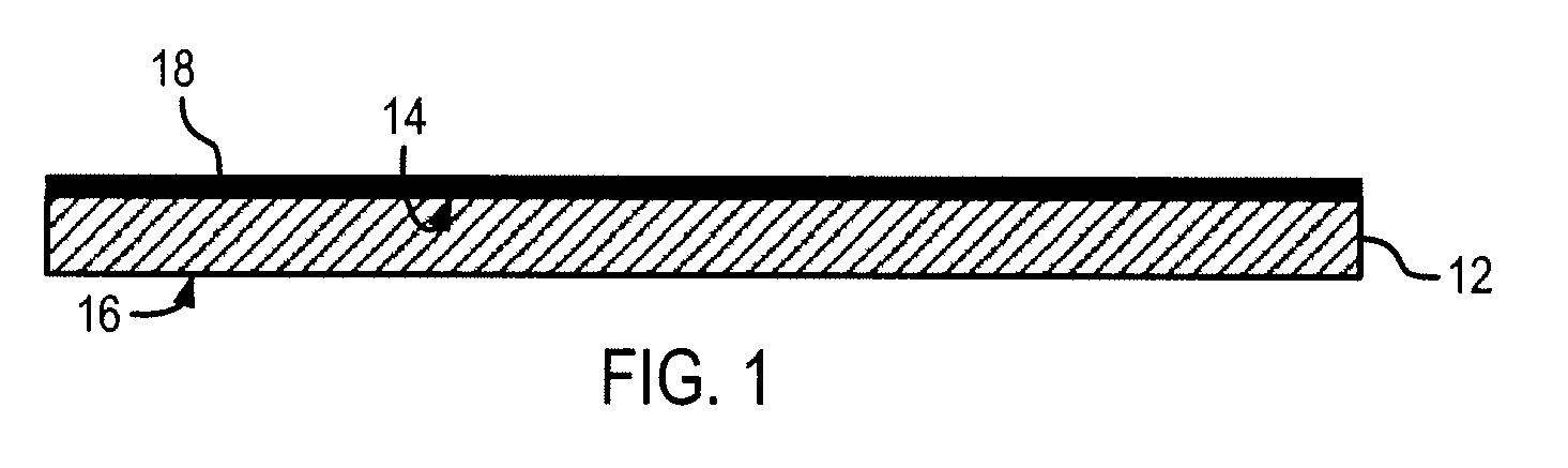
- steps in a technique for manufacturing a chip package 10 are set forth, according to an embodiment of the invention, with side cross-sectional views and top views of chip package 10 being shown at various stages of the build-up process.
- an initial flexible polymer laminate layer or dielectric substrate 12 such as Kapton®, Ultem®, polytetrafluoroethylene (PTFE), or another polymer/polyimide film, is provided.
- dielectric layer 12 comprises a top surface 14 and a bottom surface 16.
- a metal layer 18 is deposited on the top surface 14 of dielectric layer 12.
- metal layer 18 may be formed of a conductive material such as copper, titanium, chrome, and the like. Metal layer 18 may be formed on dielectric layer 12 using a sputtering and plating technique or added in any other suitable manner, such as electroplating.
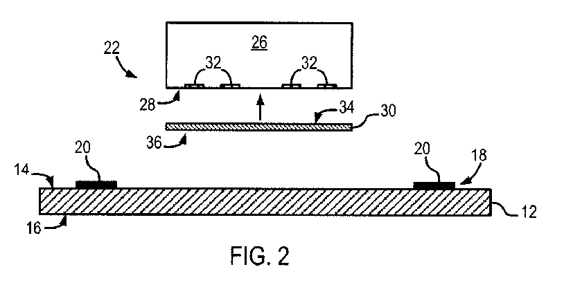
- metal layer 18 is patterned, using a common printed circuit board lithography process, for example, to form metallization paths 20.
- a die assembly 22 is aligned with a portion 24 of top surface 14 of dielectric layer 12 that is free of metallization paths 20.
- die assembly 22 includes a die 26 having an active surface 28 with an adhesive layer 30 affixed thereto.
- Active surface 28 of die 26 includes any number of die pads or contact pads 32.
- Die 26 may be any of various die types, such as, for example, a memory die type, a processing die type, a logic die type, and an application specific integrated circuit (ASIC) die type.
- ASIC application specific integrated circuit
- Adhesive layer 30 has a first surface 34 and a second surface 36 and is formed using a non-conductive adhesive material that is drillable once fully cured, such as an epoxy, for example. In one embodiment, adhesive layer 30 is partially cured after being applied to die 26. Adhesive layer 30 may be formed on active surface 28 of die 26 using a number of different techniques, as set forth in detail with respect to FIGS. 10-18 .
- die assembly 22 is affixed to dielectric layer 12 via adhesion between first surface 36 of adhesive layer 30 and top surface 14 of dielectric layer 12.
- a heated tip or collet of a pick-and-place machine or vacuum chuck is used to pick up and heat die assembly 22 prior to positioning assembly 22 on dielectric layer 12.
- heat from the vacuum chuck and/or dielectric layer 12 causes adhesive layer 30 to become tacky, and adhesive layer 30 bonds to dielectric layer 12. Any voids or air gaps between die assembly 22 and dielectric layer 12 may be removed using vacuum lamination.
- adhesive layer 30 remains tacky after being applied to die 26.
- a pick-and-place machine may be used to bond die assembly 22 to dielectric layer 12 without the need to apply heat.
- Securing die assembly 22 to dielectric layer 12 includes fully curing adhesive layer 30. As shown in FIG. 4 , adhesive layer 30 is affixed to a portion 38 of top surface 14 of dielectric layer 12 and portions 40, 42 of top surface 14, which are adjacent to portion 38, are substantially free of adhesive.
- dielectric layer 12 is patterned to form a plurality of vias 44 which are drilled either through the thickness 46 of the dielectric layer 12 or the combined thickness 48 of dielectric layer 12 and adhesive layer 30.
- vias 44 are formed at positions corresponding to metallization paths 20 and to contact pads 32 so as to expose metallization paths 20 and contact pads 32.
- vias 44 may be formed by way of other methods including plasma etching, photo-definition, or mechanical drilling processes.
- a next step of the build-up technique of chip package 10 includes the application of a second metal layer 50 to the bottom surface 16 of dielectric layer 12 by way of, for example, a sputtering or electroplating process.
- Second metallization layer 50 is subsequently patterned or etched to form metal interconnects 52.
- the metal layer/material is patterned and etched such that metal interconnects 52 are formed that extend from bottom surface 16 of dielectric layer 12 and down through vias 44.
- Metal interconnects 52 thus form an electrical connection with metallization paths 20 and contact pads 32. Together, dielectric layer 12, vias 44, and metal interconnects 52 form an initial re-distribution layer 54.
- one or more additional re-distribution layers 56 are formed on initial re-distribution layer 54 through a series of lamination and patterning steps.
- a conventional adhesive layer 58 is applied between initial re-distribution layer 54, and an additional dielectric layer 60 is applied thereto.
- a plurality of vias 62 is formed in additional dielectric layer 60, and metal interconnects 64 are formed/patterned to extend down through vias 62 and through additional dielectric layer 60 so as to electrically connect each additional re-distribution layer 56. While only one additional re-distribution layer 56 is shown in FIG. 7 , it is recognized that more re-distribution layers could be similarly applied based on a desired configuration.
- chip package 10 is illustrated as including one die 26, one skilled in the art will readily recognize that the manufacturing technique set forth with respect to FIGS. 1-7 is equally applicable for use in manufacturing a chip package with more than one die, such as multi-chip package 66 shown in FIG. 8 , which includes multiple dies 68, 70 each having contact pads 72 on respective active surfaces 74, 76.
- Multi-chip package 66 includes a re-distribution layer 78, similar to re-distribution layer 54 ( FIG. 6 ), comprising a dielectric layer 80 with vias 82 and metal interconnects 84. Similar to chip package 10 ( FIG. 6 ), metallization paths 86 formed are on a top surface 88 of dielectric layer 80.
- each die 68, 70 is attached to a dielectric layer 80, similar to dielectric layer 12 ( FIG. 1 ), by a respective adhesive layer 90, 92, similar to adhesive layer 30 ( FIG. 2 ). Because each adhesive layer 90, 92 is applied directly to a respective die 68, 70 rather than as a solid layer on top surface 88 of dielectric layer 80, adhesive 90, 92 is substantially limited to the surface area of dies 68, 70. Thus, an adhesive-free area 94 exists on top surface 88 of dielectric layer 80 and substantially surrounds dies 68, 70, as shown in FIG. 9 .
- the resulting gap 96 between respective adhesive layers 90, 92 allows dies 68, 70 to be positioned more accurately and closer together than in a package where the adhesive layer is formed across the entire surface of the dielectric layer. That is, because top surface 88 of dielectric layer 80 is free of adhesive in area 94, no continuous surface of adhesive exists between or around dies 68, 70 on which the die could swim out of position or be attracted together during the curing process.
- multiple dies 68, 70 may be configured to perform identical tasks.
- dies 68, 70 may be of one die type configured to perform memory functions or processor functions.
- dies 68, 70 are not all configured to perform identical tasks or to be of the same die type.
- a first die type may be configured to perform tasks of a first processor type
- a second die type may be configured to perform tasks of a second processor type
- a third die type may be configured to perform tasks of a memory type as examples.
- Other die types are also contemplated herein.
- Technique 98 may be used to apply adhesive layer 30 to die 26 ( FIG. 2 ) or adhesive 90, 92 to respective dies 68, 70 ( FIG. 8 ) as examples.
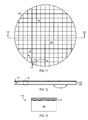
- Technique 98 begins at step 100 by applying an adhesive layer 102 to a top surface 104 of a silicon wafer 106.
- Wafer 106 is generally sliced from monosilicon crystal ingot or polysilicon crystal ingot and prepared such that a number of contact pads are positioned thereon. As shown, wafer 106 is divided into a plurality of dies 108 by scribe lines 110.
- Adhesive layer 102 is dispensed onto wafer 106 so as to cover the top surface 104 thereof. According to various embodiments, adhesive layer 102 is applied to wafer 106 in liquid form by film transfer or a spin-on or spray-coating process.
- the adhesive layer 102 is B-staged to partially cure adhesive layer 102.
- the material composition of adhesive layer 102 is selected such that adhesive layer 102 is not tacky following partial curing at step 112.
- wafer 106 is sawn or singulated into individual die assemblies 116 along scribe lines 110.
- Each die assembly 116 includes an individual die 108 with a portion of adhesive layer 102 bonded thereto.
- dies 108 are adhered to a dielectric layer, such as, for example, dielectric layer 12 of FIG. 1 , using a vacuum chuck as described with respect to FIGS. 3 and 4 . Heat from the vacuum chuck and/or dielectric layer 12 causes the partially cured adhesive layer 60 of dies 108 to become tacky, thereby allowing dies 108 to stick in position on the dielectric layer.
- steps 100, 112, 114, 118 may be repeated to position additional dies on the dielectric layer as desired.
- additional heat is applied to adhesive layer 102 to fully cure the adhesive.
- the vacuum chuck may be configured to heat dies 108 to a temperature that causes adhesive layer 102 to fully cure the adhesive after dies 108 are positioned on the dielectric layer.
- FIGS. 14-17 set forth an alternative technique 122 for applying an adhesive layer to a die.
- technique 122 begins at step 124 by applying an adhesive layer 126 to a top or active surface 128 of a silicon wafer 130, which is divided into a plurality of dies 132 via scribe lines 134 in a similar manner as wafer 106 ( FIG. 12 ).
- Adhesive layer 126 is applied to top surface 128 of wafer 130 in a similar manner as described above with respect to step 100 of technique 98.
- adhesive layer 126 is partially cured. The catalyst ratio in adhesive layer 126 is selected such that adhesive layer 102 remains tacky following the partial cure.
- a release sheet 140 is applied to the tacky surface 142 of adhesive layer 126 using low temperature lamination, roll lamination, or other similar technique.
- wafer 130 is sawn from the back side 146 into individual dies 132.
- An infrared camera may be used to locate scribe lines 134 and align the saw to wafer 130. The saw singulates wafer 130 such that the release sheet 140 remains intact and individual die assemblies 148 remain on release sheet 140 after dies 132 are singulated.
- each die assembly 148 comprises a die 132 with an adhesive layer 126 adhered thereto.
- a vacuum collect picks up individual die assemblies 148 for placement on a dielectric layer, such as dielectric layer 12 of FIG. 1 .
- a dielectric layer such as dielectric layer 12 of FIG. 1 .
- the vacuum chuck places the respective die assembly 148 adhesive layer side down onto the dielectric layer. After all desired dies are positioned on the dielectric layer using the process set forth in steps 124, 136, 138, 144, and 150, adhesive layer 126 is fully cured at step 152.
- an alternative technique 154 for applying an adhesive layer to a die prior to attaching the die to a dielectric layer is set forth.
- a release sheet is positioned on the processing system and coated with a layer of adhesive.
- the adhesive layer is partially cured to B-stage at step 158 and remains tacky after partial curing.
- a pick-and-place system is used to pick up a singulated die on the back surface of the die and touch down the active surface of the die into the tacky adhesive, thereby coating the active surface with adhesive.
- the adhesive-coated die is positioned adhesive side down onto the dielectric layer at step 162. After all desired die are positioned on the dielectric layer using the process set forth in steps 156-162, the adhesive is fully cured at step 164.
- a pick-and-place system is used to pick up a singulated die and touch the active surface of the die into a pot of liquid or paste adhesive, rather than an adhesive-coated release sheet as described above.
- the pick-and-place system then transfers the adhesive-coated die to the dielectric layer with or without applying heat to the die. Heating the die during the transfer process gets rid of extra solvent in the adhesive that may cause the die to "swim" or move out of position after being placed on the dielectric layer.
- a dielectric layer 166 is provided, similar to dielectric layer 12 ( FIG. 1 ). As shown in FIG. 19 , dielectric layer 166 comprises a top surface 168 and a bottom surface 170. According to an optional step of the build-up process, a pre-patterned metal layer 172, similar to metal layer 18 ( FIG. 1 ) may be deposited on the top surface 168 of dielectric layer 166.
- FIG. 20 a metal screen 174 having openings 176 formed therein is aligned atop top surface 168 of dielectric layer 166.
- FIG. 25 illustrates a top view of a portion of metal screen 174 corresponding to the cross-sectional view of FIG. 20 .
- openings 176 in metal screen 174 are sized to correspond to the surface area of corresponding die, as described in more detail below.
- metal screen 174 is aligned with dielectric layer 166 such that openings 176 are positioned atop corresponding die pocket locations 178 on top surface 168 of dielectric layer 166.
- adhesive 180 is dispensed along an edge 182 of metal screen 174.
- a squeegee 184 is brought into place adjacent adhesive 180.
- Squeegee 184 is drawn across metal screen 174, leaving a layer of adhesive 186 in respective die pockets 178, as shown in FIG. 21 .
- metal screen 174 is separated from dielectric layer 166 and removed. As shown in FIG. 22 , an adhesive-free gap 188 is formed between adjacent portions of the resulting adhesive layer 186. After metal screen 174 is removed, adhesive layer 186 is B stage cured to a tacky state.
- dies 190, 192 are aligned with die locations 178 and respective portions of adhesive layer 186, as shown in FIG. 23 , using a pick-and-place machine or vacuum chuck. As shown, each die 190, 192 has an active surface 194 with any number of die pads 196. Similar to die 26 of FIG. 2 , die 190, 192 may be any of various die types, such as, for example, a memory die type, a processing die type, a logic die type, and an application specific integrated circuit (ASIC) die type. Referring to FIG. 24 , after die 190, 192 are positioned atop adhesive 186, adhesive 186 is fully cured. As one skilled in the art will readily recognize, in subsequent steps of the build-up technique, vias and metallization paths may be formed on dielectric layer 166 in a similar manner as described with respect to FIG. 6 to form a chip package such as chip package 10.
- ASIC application specific integrated circuit
- a dielectric layer 198 is provided, similar to dielectric layer 12 ( FIG. 1 ), having a top surface 200 and a bottom surface 202.
- a metal layer 204 may be deposited or pre-patterned on top surface 168 of dielectric layer 198.
- an inkjet printerhead 206 filled with adhesive 208 is positioned at an edge 210 of dielectric layer 198, as shown in FIG. 27 .
- adhesive 208 is dispensed in a pattern across top surface 200 of dielectric layer 198 at respective die locations 212.
- adhesive 208 is dispensed such that a gap 214 is formed on top surface top surface 200 of dielectric layer 198 between adjacent die locations 212. Gap 214 is substantially free of adhesive.
- Adhesive 208 is then B stage cured to a tacky state.
- dies 216, 218 having any number of contact pads 220 are aligned with adhesive 208.
- the respective active surface 222 of each die 216, 218 is placed into adhesive 208 using a pick-and-place machine or vacuum chuck, as shown in FIG. 29 .
- Adhesive 208 is subsequently fully cured.
- vias and metallization paths may be formed on dielectric layer 198 in a similar manner as described with respect to FIG. 6 to form a chip package such as chip package 10.
- a release sheet 224 is coated with an adhesive layer 226.
- Adhesive layer 226 is then baked to B stage to partially cure adhesive layer 226.
- Adhesive layer 226 may be baked to a tacky state or non-tacky state, according to various embodiments.
- adhesive layer 226 is scribed or cut (e.g., via a laser) into individual adhesive portions 228 sized to substantially match the surface area of the active surface 230 of individual dies 232, 234 ( FIG. 34 ).
- top surface 236 of a polyimide flex layer or dielectric layer 238 has a pre-patterned metal interconnection layer 246 formed thereon.
- dies 232, 234 are aligned with respective die locations 240, 242 using, for example, a vacuum chuck or pick-and-place machine, as shown in FIG. 34 .
- adhesive layer 226 was cured to a tacky state
- the respective active surfaces 230 of dies 232, 234 are placed into respective adhesive portions 228.
- dies 232, 234 and/or dielectric layer 238 are heated prior to placement of dies 232, 234. Heat from dies 232, 234 and/or dielectric layer 238 causes adhesive portions 228 to become tacky and dies 232, 234 to bond to adhesive portions 228, as shown in FIG. 35 .
- Adhesive portions 228 are then fully cured.
- vias and metallization paths may be formed on dielectric layer 238 in a similar manner as described with respect to FIG. 6 to form a chip package such as chip package 10.
- embodiments of the invention overcome the aforementioned drawbacks in the prior art of coating the entire dielectric layer with adhesive by providing a method of chip fabrication in which the adhesive is applied directly to one of the active surface of the die and select portions of the dielectric layer corresponding to die locations prior to positioning the die on the dielectric layer.
- the surface of the dielectric substrate of the resulting integrated circuit device has at least one portion with adhesive thereon and at least one portion that is substantially free of adhesive.
- a chip package includes a first die comprising an active surface having at least one die pad positioned thereon; a first adhesive layer having a first surface coupled to the active surface of the first die and a second surface opposite the first surface; and a first dielectric layer having a top surface, wherein a first portion of the top surface of the first dielectric layer is coupled to the second surface of the first adhesive layer. A second portion of the top surface of the first dielectric layer, distinct from the first portion, is substantially free of adhesive.
- a method of forming an integrated chip package includes providing a first semiconductor die comprising an active surface having at least one contact pad positioned thereon, applying an adhesive layer to the active surface of the first semiconductor die, and adhering the first semiconductor die having the adhesive layer applied thereto to a top surface of a dielectric substrate by way of the adhesive layer.
- an integrated chip package includes a dielectric substrate and a first die assembly.
- the first die assembly includes a semiconductor die having an active surface with contact pads positioned thereon and a non-conductive adhesive layer having a first surface coupled to the active surface of the semiconductor die.
- a surface area of the first surface of the adhesive layer is substantially equal to a surface area of the active surface of the semiconductor die.
- a second surface of the adhesive layer, opposite the first surface, is coupled to a surface of the dielectric substrate.
- a subportion of the surface of the flexible substrate adjacent to the first die assembly is substantially free of adhesive.
- a method of forming an integrated chip package includes providing a dielectric substrate having a die location positioned on a top surface thereof, providing a first semiconductor die comprising an active surface having at least one contact pad positioned thereon, and applying an adhesive layer to one of the active surface of the first semiconductor die and the die location of the dielectric substrate.
- the adhesive layer has a surface area approximately equal to the surface area of the active surface of the first semiconductor die.
- the method further includes adhering the first semiconductor die to the top surface of the dielectric substrate by way of the adhesive layer.
- a method of forming an integrated chip package includes providing a dielectric substrate having a plurality of die locations positioned on a surface thereof and applying a patterned adhesive layer onto the plurality of die locations of the dielectric substrate such that a gap is formed on the surface of the dielectric substrate between adjacent die locations, the gap being substantially free of adhesive.
- the method also includes adhering a plurality of semiconductor dies to the dielectric substrate via the adhesive layer.
Landscapes
- Die Bonding (AREA)
- Engineering & Computer Science (AREA)
- Manufacturing & Machinery (AREA)
- Physics & Mathematics (AREA)
- Geometry (AREA)
- Wire Bonding (AREA)
- Production Of Multi-Layered Print Wiring Board (AREA)
Abstract


Description
- Embodiments of the invention relate generally to integrated circuit packages and, more particularly, to adhesive placement within the integrated circuit package.
- As integrated circuits become increasingly smaller and yield better operating performance, packaging technology for integrated circuit (IC) packaging has correspondingly evolved from leaded packaging to laminated-based ball grid array (BGA) packaging and eventually to chip scale packaging (CSP). Advancements in IC chip packaging technology are driven by ever-increasing needs for achieving better performance, greater miniaturization, and higher reliability. New packaging technology has to further provide for the possibilities of batch production for the purpose of large-scale manufacturing thereby allowing economy of scale.
- A standard CSP manufacturing process typically begins by mounting a dielectric substrate or flex layer to a frame that stabilizes the substrate during the manufacturing process. An adhesive is dispensed in liquid form onto the surface of the dielectric substrate and the frame is spun rapidly to spread the liquid adhesive to a uniform thickness across the entire surface of the dielectric. Next, one or more dies are positioned active side down into the adhesive and the adhesive is cured. A plurality of re-distribution layers are then deposited onto the dielectric substrate and patterned to form a thin-film metal re-routing and interconnection system, with eight or more re-distribution layers being common. The re-distribution layers are typically formed from a benzocyclobutene (BCB) or polyimide material, for example, and applied via a spin-on or lamination application process. The electrical connection between the laminate re-distribution layers and the die(s) form an input/output (I/O) system to and from the die(s).
- Advancements in IC packaging requirements pose challenges to the existing embedded chip build-up process. As IC packages become thinner, the adhesive layer may cause the IC package to warp or otherwise become distorted as a result of uneven stress distributions on the top and bottom surfaces of the dielectric layer. Further, in order to manufacture smaller and more complex multi-chip IC packages, dies must be positioned more closely together and with great precision on the dielectric. However, the adhesive layer that couples the dies to the dielectric can make precise alignment of closely spaced dies difficult. For example, when two or more dies are positioned in close proximity to one another on the dielectric, the dies have a tendency to "swim" or move out of the desired position during the adhesive curing process. In addition to merely moving out of the desired position, closely spaced dies may be attracted to one another while the adhesive is curing, a phenomenon that may cause the undesired result of dies touching or becoming stuck to one another in the final chip package.
- Accordingly, there is a need for a method of chip package fabrication that minimizes the warpage and distortion that can be caused by the adhesive layer and that allows for closer die spacing and precise die alignment in the IC package. There is a further need for the fabrication method to be readily incorporated into an assembly process, minimize processing time, and provide for a low cost assembly.
- In accordance with one aspect of the invention, a chip package includes a first die comprising an active surface having at least one die pad positioned thereon; a first adhesive layer having a first surface coupled to the active surface of the first die and a second surface opposite the first surface; and a first dielectric layer having a top surface, wherein a first portion of the top surface of the first dielectric layer is coupled to the second surface of the first adhesive layer. A second portion of the top surface of the first dielectric layer, distinct from the first portion, is substantially free of adhesive
- In accordance with another aspect of the invention, a method of forming an integrated chip package includes providing a first semiconductor die comprising an active surface having at least one contact pad positioned thereon, applying an adhesive layer to the active surface of the first semiconductor die, and adhering the first semiconductor die having the adhesive layer applied thereto to a top surface of a dielectric substrate by way of the adhesive layer.
- In accordance with another aspect of the invention, an integrated chip package includes a dielectric substrate and a first die assembly. The first die assembly includes a semiconductor die having an active surface with contact pads positioned thereon and a non-conductive adhesive layer having a first surface coupled to the active surface of the semiconductor die. A surface area of the first surface of the adhesive layer is substantially equal to a surface area of the active surface of the semiconductor die. A second surface of the adhesive layer, opposite the first surface, is coupled to a surface of the dielectric substrate. A subportion of the surface of the flexible substrate adjacent to the first die assembly is substantially free of adhesive.
- In accordance with another aspect of the invention, a method of forming an integrated chip package includes providing a dielectric substrate having a die location positioned on a top surface thereof, providing a first semiconductor die comprising an active surface having at least one contact pad positioned thereon, and applying an adhesive layer to one of the active surface of the first semiconductor die and the die location of the dielectric substrate. The adhesive layer has a surface area approximately equal to the surface area of the active surface of the first semiconductor die. The method further includes adhering the first semiconductor die to the top surface of the dielectric substrate by way of the adhesive layer.
- In accordance with another aspect of the invention, a method of forming an integrated chip package includes providing a dielectric substrate having a plurality of die locations positioned on a surface thereof and applying a patterned adhesive layer onto the plurality of die locations of the dielectric substrate such that a gap is formed on the surface of the dielectric substrate between adjacent die locations, the gap being substantially free of adhesive. The method also includes adhering a plurality of semiconductor dies to the dielectric substrate via the adhesive layer.
- Various other features and advantages will be made apparent from the following detailed description and the drawings.
- The drawings illustrate embodiments presently contemplated for carrying out the invention.
- In the drawings:
-
FIGS. 1-7 are schematic diagrams showing steps of making an integrated chip package in accordance with an embodiment of the invention. -
FIG. 8 is a sectional view of an integrated multi-chip package in accordance with an embodiment of the invention. -
FIG. 9 is a bottom view of the integrated multi-chip package ofFIG. 8 . -
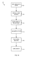
FIG. 10 is a flow chart illustrating steps of making an integrated chip package in accordance with an embodiment of the invention. -
FIG. 11 is a bottom view of a wafer assembly according to an embodiment of the invention. -
FIG. 12 is a sectional view of the wafer assembly ofFIG. 11 . -
FIG. 13 is a sectional view of a die assembly sawn from the wafer assembly ofFIG. 11 . -
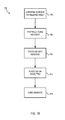
FIG. 14 is a flow chart illustrating steps of making an integrated chip package in accordance with another embodiment of the invention. -
FIG. 15 is a bottom view of a wafer assembly according to an embodiment of the invention. -
FIG. 16 is a sectional view of the wafer assembly ofFIG. 15 . -
FIG. 17 is a sectional view of a die assembly sawn from the wafer assembly ofFIG. 15 . -
FIG. 18 is a flow chart illustrating steps of making an integrated chip package in accordance with yet another embodiment of the invention. -
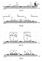
FIGS. 19-24 are schematic diagrams showing steps of a build-up process for an integrated chip package in accordance with another embodiment of the invention. -
FIG. 25 is a top view of a portion of a metal screen used to dispense a layer of adhesive in accordance with the embodiment set forth inFIGS. 19-24 . -
FIGS. 26-29 are schematic diagrams showing steps of a build-up process for an integrated chip package in accordance with another embodiment of the invention. -
FIG. 30 is a top view diagram of a release sheet coated with an adhesive layer in accordance with an embodiment of the invention. -
FIG. 31 is a top view diagram of the adhesive-coated release sheet ofFIG. 30 after scribing the adhesive layer into die sizes. -
FIGS. 32-35 are schematic diagrams showing steps of a build-up process for an integrated chip package in accordance with yet another embodiment of the invention. - Referring to
FIGS. 1-7 , steps in a technique for manufacturing a chip package 10 (i.e., a chip build-up) are set forth, according to an embodiment of the invention, with side cross-sectional views and top views ofchip package 10 being shown at various stages of the build-up process. Referring toFIG. 1 , an initial flexible polymer laminate layer ordielectric substrate 12, such as Kapton®, Ultem®, polytetrafluoroethylene (PTFE), or another polymer/polyimide film, is provided. As shown inFIG. 1 ,dielectric layer 12 comprises atop surface 14 and abottom surface 16. According to the build-up process, ametal layer 18 is deposited on thetop surface 14 ofdielectric layer 12. According to various embodiments,metal layer 18 may be formed of a conductive material such as copper, titanium, chrome, and the like.Metal layer 18 may be formed ondielectric layer 12 using a sputtering and plating technique or added in any other suitable manner, such as electroplating. - Referring to
FIG. 2 ,metal layer 18 is patterned, using a common printed circuit board lithography process, for example, to formmetallization paths 20. Next, a dieassembly 22 is aligned with aportion 24 oftop surface 14 ofdielectric layer 12 that is free ofmetallization paths 20. As shown, dieassembly 22 includes a die 26 having anactive surface 28 with anadhesive layer 30 affixed thereto.Active surface 28 ofdie 26 includes any number of die pads orcontact pads 32.Die 26 may be any of various die types, such as, for example, a memory die type, a processing die type, a logic die type, and an application specific integrated circuit (ASIC) die type.Adhesive layer 30 has afirst surface 34 and asecond surface 36 and is formed using a non-conductive adhesive material that is drillable once fully cured, such as an epoxy, for example. In one embodiment,adhesive layer 30 is partially cured after being applied to die 26.Adhesive layer 30 may be formed onactive surface 28 ofdie 26 using a number of different techniques, as set forth in detail with respect toFIGS. 10-18 . - Referring now to
FIGS. 3 and 4 , in a next step of the build-up technique ofchip package 10, dieassembly 22 is affixed todielectric layer 12 via adhesion betweenfirst surface 36 ofadhesive layer 30 andtop surface 14 ofdielectric layer 12. In one embodiment, a heated tip or collet of a pick-and-place machine or vacuum chuck is used to pick up and heat dieassembly 22 prior topositioning assembly 22 ondielectric layer 12. Whenheated die assembly 22 is placed onportion 24 ofdielectric layer 12, heat from the vacuum chuck and/ordielectric layer 12 causesadhesive layer 30 to become tacky, andadhesive layer 30 bonds todielectric layer 12. Any voids or air gaps betweendie assembly 22 anddielectric layer 12 may be removed using vacuum lamination. In an alternate embodiment,adhesive layer 30 remains tacky after being applied to die 26. Thus, a pick-and-place machine may be used to bond dieassembly 22 todielectric layer 12 without the need to apply heat. - Securing
die assembly 22 todielectric layer 12 includes fully curingadhesive layer 30. As shown inFIG. 4 ,adhesive layer 30 is affixed to aportion 38 oftop surface 14 ofdielectric layer 12 andportions top surface 14, which are adjacent toportion 38, are substantially free of adhesive. - Referring now to
FIG. 5 ,dielectric layer 12 is patterned to form a plurality ofvias 44 which are drilled either through thethickness 46 of thedielectric layer 12 or the combinedthickness 48 ofdielectric layer 12 andadhesive layer 30. According to an exemplary embodiment, vias 44 are formed at positions corresponding to metallizationpaths 20 and to contactpads 32 so as to exposemetallization paths 20 andcontact pads 32. Alternatively, it is also recognized thatvias 44 may be formed by way of other methods including plasma etching, photo-definition, or mechanical drilling processes. - As shown in
FIG. 6 , a next step of the build-up technique ofchip package 10 includes the application of asecond metal layer 50 to thebottom surface 16 ofdielectric layer 12 by way of, for example, a sputtering or electroplating process.Second metallization layer 50 is subsequently patterned or etched to form metal interconnects 52. According to one embodiment of the invention, the metal layer/material is patterned and etched such that metal interconnects 52 are formed that extend frombottom surface 16 ofdielectric layer 12 and down throughvias 44. Metal interconnects 52 thus form an electrical connection withmetallization paths 20 andcontact pads 32. Together,dielectric layer 12, vias 44, andmetal interconnects 52 form aninitial re-distribution layer 54. - As further shown in
FIG. 7 , in an optional next step of the manufacturing technique, one or more additionalre-distribution layers 56 are formed oninitial re-distribution layer 54 through a series of lamination and patterning steps. Aconventional adhesive layer 58 is applied between initialre-distribution layer 54, and anadditional dielectric layer 60 is applied thereto. A plurality ofvias 62 is formed in additionaldielectric layer 60, andmetal interconnects 64 are formed/patterned to extend down throughvias 62 and through additionaldielectric layer 60 so as to electrically connect eachadditional re-distribution layer 56. While only oneadditional re-distribution layer 56 is shown inFIG. 7 , it is recognized that more re-distribution layers could be similarly applied based on a desired configuration. - While
chip package 10 is illustrated as including onedie 26, one skilled in the art will readily recognize that the manufacturing technique set forth with respect toFIGS. 1-7 is equally applicable for use in manufacturing a chip package with more than one die, such asmulti-chip package 66 shown inFIG. 8 , which includes multiple dies 68, 70 each havingcontact pads 72 on respectiveactive surfaces 74, 76.Multi-chip package 66 includes are-distribution layer 78, similar to re-distribution layer 54 (FIG. 6 ), comprising adielectric layer 80 withvias 82 and metal interconnects 84. Similar to chip package 10 (FIG. 6 ),metallization paths 86 formed are on atop surface 88 ofdielectric layer 80. - As shown, each die 68, 70 is attached to a
dielectric layer 80, similar to dielectric layer 12 (FIG. 1 ), by a respectiveadhesive layer FIG. 2 ). Because eachadhesive layer respective die top surface 88 ofdielectric layer 80, adhesive 90, 92 is substantially limited to the surface area of dies 68, 70. Thus, an adhesive-free area 94 exists ontop surface 88 ofdielectric layer 80 and substantially surrounds dies 68, 70, as shown inFIG. 9 . - The resulting
gap 96 between respectiveadhesive layers top surface 88 ofdielectric layer 80 is free of adhesive inarea 94, no continuous surface of adhesive exists between or around dies 68, 70 on which the die could swim out of position or be attracted together during the curing process. - According to an embodiment of the invention, multiple dies 68, 70 may be configured to perform identical tasks. For example, dies 68, 70 may be of one die type configured to perform memory functions or processor functions. However, according to another embodiment of the invention, dies 68, 70 are not all configured to perform identical tasks or to be of the same die type. For example, a first die type may be configured to perform tasks of a first processor type, a second die type may be configured to perform tasks of a second processor type, and a third die type may be configured to perform tasks of a memory type as examples. Other die types are also contemplated herein.
- Referring now to
FIGS. 10-13 simultaneously, atechnique 98 for applying an adhesive layer to a die is set forth according to an embodiment of the invention.Technique 98 may be used to applyadhesive layer 30 to die 26 (FIG. 2 ) or adhesive 90, 92 to respective dies 68, 70 (FIG. 8 ) as examples.Technique 98 begins atstep 100 by applying anadhesive layer 102 to atop surface 104 of asilicon wafer 106.Wafer 106 is generally sliced from monosilicon crystal ingot or polysilicon crystal ingot and prepared such that a number of contact pads are positioned thereon. As shown,wafer 106 is divided into a plurality of dies 108 byscribe lines 110.Adhesive layer 102 is dispensed ontowafer 106 so as to cover thetop surface 104 thereof. According to various embodiments,adhesive layer 102 is applied towafer 106 in liquid form by film transfer or a spin-on or spray-coating process. - At
step 112, afterwafer 106 is coated withadhesive layer 102, theadhesive layer 102 is B-staged to partially cureadhesive layer 102. The material composition ofadhesive layer 102 is selected such thatadhesive layer 102 is not tacky following partial curing atstep 112. - At
step 114,wafer 106 is sawn or singulated intoindividual die assemblies 116 along scribe lines 110. Eachdie assembly 116 includes anindividual die 108 with a portion ofadhesive layer 102 bonded thereto. Atstep 118, dies 108 are adhered to a dielectric layer, such as, for example,dielectric layer 12 ofFIG. 1 , using a vacuum chuck as described with respect toFIGS. 3 and 4 . Heat from the vacuum chuck and/ordielectric layer 12 causes the partially curedadhesive layer 60 of dies 108 to become tacky, thereby allowing dies 108 to stick in position on the dielectric layer. - The process set forth in
steps adhesive layer 102 to fully cure the adhesive. Alternatively, the vacuum chuck may be configured to heat dies 108 to a temperature that causesadhesive layer 102 to fully cure the adhesive after dies 108 are positioned on the dielectric layer. -
FIGS. 14-17 set forth analternative technique 122 for applying an adhesive layer to a die. Referring toFIGS. 14-17 ,technique 122 begins atstep 124 by applying anadhesive layer 126 to a top oractive surface 128 of asilicon wafer 130, which is divided into a plurality of dies 132 viascribe lines 134 in a similar manner as wafer 106 (FIG. 12 ).Adhesive layer 126 is applied totop surface 128 ofwafer 130 in a similar manner as described above with respect to step 100 oftechnique 98. Atstep 136,adhesive layer 126 is partially cured. The catalyst ratio inadhesive layer 126 is selected such thatadhesive layer 102 remains tacky following the partial cure. - At
step 138, arelease sheet 140 is applied to thetacky surface 142 ofadhesive layer 126 using low temperature lamination, roll lamination, or other similar technique. Atstep 144,wafer 130 is sawn from theback side 146 into individual dies 132. An infrared camera may be used to locatescribe lines 134 and align the saw towafer 130. Thesaw singulates wafer 130 such that therelease sheet 140 remains intact andindividual die assemblies 148 remain onrelease sheet 140 after dies 132 are singulated. As shown, each dieassembly 148 comprises a die 132 with anadhesive layer 126 adhered thereto. - At
step 150, a vacuum collect picks upindividual die assemblies 148 for placement on a dielectric layer, such asdielectric layer 12 ofFIG. 1 . As each dieassembly 148 is removed fromrelease sheet 140, a portion ofadhesive layer 126 transfers fromrelease sheet 140 to theactive surface 128 of thecorresponding die 132. The vacuum chuck then places therespective die assembly 148 adhesive layer side down onto the dielectric layer. After all desired dies are positioned on the dielectric layer using the process set forth insteps adhesive layer 126 is fully cured atstep 152. - Referring now to
FIG. 18 , analternative technique 154 for applying an adhesive layer to a die prior to attaching the die to a dielectric layer is set forth. Atstep 156, a release sheet is positioned on the processing system and coated with a layer of adhesive. The adhesive layer is partially cured to B-stage atstep 158 and remains tacky after partial curing. - At
step 160, a pick-and-place system is used to pick up a singulated die on the back surface of the die and touch down the active surface of the die into the tacky adhesive, thereby coating the active surface with adhesive. The adhesive-coated die is positioned adhesive side down onto the dielectric layer atstep 162. After all desired die are positioned on the dielectric layer using the process set forth in steps 156-162, the adhesive is fully cured at step 164. - In an alternative embodiment, a pick-and-place system is used to pick up a singulated die and touch the active surface of the die into a pot of liquid or paste adhesive, rather than an adhesive-coated release sheet as described above. The pick-and-place system then transfers the adhesive-coated die to the dielectric layer with or without applying heat to the die. Heating the die during the transfer process gets rid of extra solvent in the adhesive that may cause the die to "swim" or move out of position after being placed on the dielectric layer.
- Referring now to
FIGS. 19-24 , steps in an alternative technique for manufacturing a chip package, such as chip package 10 (FIG. 6 ) are set forth, according to an embodiment of the invention, with side cross-sectional views shown at various stages of the build-up process. Referring toFIG. 19 , adielectric layer 166 is provided, similar to dielectric layer 12 (FIG. 1 ). As shown inFIG. 19 ,dielectric layer 166 comprises atop surface 168 and abottom surface 170. According to an optional step of the build-up process, apre-patterned metal layer 172, similar to metal layer 18 (FIG. 1 ) may be deposited on thetop surface 168 ofdielectric layer 166. - Referring to
FIG. 20 , ametal screen 174 havingopenings 176 formed therein is aligned atoptop surface 168 ofdielectric layer 166.FIG. 25 illustrates a top view of a portion ofmetal screen 174 corresponding to the cross-sectional view ofFIG. 20 . As shown,openings 176 inmetal screen 174 are sized to correspond to the surface area of corresponding die, as described in more detail below. - Referring back to
FIG. 20 ,metal screen 174 is aligned withdielectric layer 166 such thatopenings 176 are positioned atop correspondingdie pocket locations 178 ontop surface 168 ofdielectric layer 166. In a next step of the build-up technique, adhesive 180 is dispensed along anedge 182 ofmetal screen 174. Asqueegee 184 is brought into placeadjacent adhesive 180.Squeegee 184 is drawn acrossmetal screen 174, leaving a layer of adhesive 186 in respective diepockets 178, as shown inFIG. 21 . - Referring now to
FIG. 22 , in a next step of the build-up technique ofchip package 10,metal screen 174 is separated fromdielectric layer 166 and removed. As shown inFIG. 22 , an adhesive-free gap 188 is formed between adjacent portions of the resultingadhesive layer 186. Aftermetal screen 174 is removed,adhesive layer 186 is B stage cured to a tacky state. - Next, dies 190, 192 are aligned with
die locations 178 and respective portions ofadhesive layer 186, as shown inFIG. 23 , using a pick-and-place machine or vacuum chuck. As shown, each die 190, 192 has anactive surface 194 with any number ofdie pads 196. Similar to die 26 ofFIG. 2 , die 190, 192 may be any of various die types, such as, for example, a memory die type, a processing die type, a logic die type, and an application specific integrated circuit (ASIC) die type. Referring toFIG. 24 , afterdie dielectric layer 166 in a similar manner as described with respect toFIG. 6 to form a chip package such aschip package 10. - Referring now to
FIGS. 26-29 , steps in an alternative technique for manufacturing a chip package, such as chip package 10 (FIG. 6 ) are set forth, according to another embodiment of the invention, with side cross-sectional views ofchip package 10 being shown at various stages of the build-up process. Referring toFIG. 25 , adielectric layer 198 is provided, similar to dielectric layer 12 (FIG. 1 ), having atop surface 200 and abottom surface 202. Optionally, ametal layer 204 may be deposited or pre-patterned ontop surface 168 ofdielectric layer 198. - In a next step of the build-up technique, an
inkjet printerhead 206 filled with adhesive 208 is positioned at anedge 210 ofdielectric layer 198, as shown inFIG. 27 . Asinkjet 206 printer head travels acrossdielectric layer 198, adhesive 208 is dispensed in a pattern acrosstop surface 200 ofdielectric layer 198 atrespective die locations 212. As shown inFIG. 28 , adhesive 208 is dispensed such that agap 214 is formed on top surfacetop surface 200 ofdielectric layer 198 between adjacentdie locations 212.Gap 214 is substantially free of adhesive. -
Adhesive 208 is then B stage cured to a tacky state. Next, dies 216, 218 having any number ofcontact pads 220 are aligned withadhesive 208. The respectiveactive surface 222 of each die 216, 218 is placed into adhesive 208 using a pick-and-place machine or vacuum chuck, as shown inFIG. 29 .Adhesive 208 is subsequently fully cured. As one skilled in the art will readily recognize, in subsequent steps of the build-up technique, vias and metallization paths may be formed ondielectric layer 198 in a similar manner as described with respect toFIG. 6 to form a chip package such aschip package 10. - Referring now to
FIGS. 30-35 , steps in an alternative technique for manufacturing a chip package are set forth, according to yet another embodiment of the invention. Referring first toFIG. 30 , arelease sheet 224 is coated with anadhesive layer 226.Adhesive layer 226 is then baked to B stage to partially cureadhesive layer 226.Adhesive layer 226 may be baked to a tacky state or non-tacky state, according to various embodiments. In a next step of the manufacturing process,adhesive layer 226 is scribed or cut (e.g., via a laser) into individualadhesive portions 228 sized to substantially match the surface area of theactive surface 230 of individual dies 232, 234 (FIG. 34 ). - Referring now to
FIGS. 32 and 33 ,adhesive portions 228 are positioned on atop surface 236 of a polyimide flex layer ordielectric layer 238 atrespective die locations gap 244 ondielectric layer 238 between adjacentadhesive portions 228. In one embodiment,top surface 236 ofdielectric layer 238 has a pre-patternedmetal interconnection layer 246 formed thereon. In a next step of the manufacturing process, dies 232, 234 are aligned withrespective die locations FIG. 34 . In an embodiment whereadhesive layer 226 was cured to a tacky state, the respectiveactive surfaces 230 of dies 232, 234 are placed into respectiveadhesive portions 228. In an embodiment whereadhesive layer 226 was cured to a non-tacky state, dies 232, 234 and/ordielectric layer 238 are heated prior to placement of dies 232, 234. Heat from dies 232, 234 and/ordielectric layer 238 causesadhesive portions 228 to become tacky and dies 232, 234 to bond toadhesive portions 228, as shown inFIG. 35 .Adhesive portions 228 are then fully cured. As one skilled in the art will readily recognize, in subsequent steps of the build-up technique, vias and metallization paths may be formed ondielectric layer 238 in a similar manner as described with respect toFIG. 6 to form a chip package such aschip package 10. - Accordingly, embodiments of the invention overcome the aforementioned drawbacks in the prior art of coating the entire dielectric layer with adhesive by providing a method of chip fabrication in which the adhesive is applied directly to one of the active surface of the die and select portions of the dielectric layer corresponding to die locations prior to positioning the die on the dielectric layer. Thus, the surface of the dielectric substrate of the resulting integrated circuit device has at least one portion with adhesive thereon and at least one portion that is substantially free of adhesive. Applying adhesive to the die directly simplifies the processing steps, reduces subsequent processing steps, allows dies to be placed more closely together, and significantly reduces the amount of adhesive on the surface of the dielectric layer, thereby minimizing unbalanced stresses and reducing material costs.
- Therefore, according to one embodiment of the invention, a chip package includes a first die comprising an active surface having at least one die pad positioned thereon; a first adhesive layer having a first surface coupled to the active surface of the first die and a second surface opposite the first surface; and a first dielectric layer having a top surface, wherein a first portion of the top surface of the first dielectric layer is coupled to the second surface of the first adhesive layer. A second portion of the top surface of the first dielectric layer, distinct from the first portion, is substantially free of adhesive.
- According to another embodiment of the invention, a method of forming an integrated chip package includes providing a first semiconductor die comprising an active surface having at least one contact pad positioned thereon, applying an adhesive layer to the active surface of the first semiconductor die, and adhering the first semiconductor die having the adhesive layer applied thereto to a top surface of a dielectric substrate by way of the adhesive layer.
- According to yet another embodiment of the invention, an integrated chip package includes a dielectric substrate and a first die assembly. The first die assembly includes a semiconductor die having an active surface with contact pads positioned thereon and a non-conductive adhesive layer having a first surface coupled to the active surface of the semiconductor die. A surface area of the first surface of the adhesive layer is substantially equal to a surface area of the active surface of the semiconductor die. A second surface of the adhesive layer, opposite the first surface, is coupled to a surface of the dielectric substrate. A subportion of the surface of the flexible substrate adjacent to the first die assembly is substantially free of adhesive.
- According to yet another embodiment of the invention, a method of forming an integrated chip package includes providing a dielectric substrate having a die location positioned on a top surface thereof, providing a first semiconductor die comprising an active surface having at least one contact pad positioned thereon, and applying an adhesive layer to one of the active surface of the first semiconductor die and the die location of the dielectric substrate. The adhesive layer has a surface area approximately equal to the surface area of the active surface of the first semiconductor die. The method further includes adhering the first semiconductor die to the top surface of the dielectric substrate by way of the adhesive layer.
- According to yet another embodiment of the invention, a method of forming an integrated chip package includes providing a dielectric substrate having a plurality of die locations positioned on a surface thereof and applying a patterned adhesive layer onto the plurality of die locations of the dielectric substrate such that a gap is formed on the surface of the dielectric substrate between adjacent die locations, the gap being substantially free of adhesive. The method also includes adhering a plurality of semiconductor dies to the dielectric substrate via the adhesive layer.
- This written description uses examples to disclose the invention, including the best mode, and also to enable any person skilled in the art to practice the invention, including making and using any devices or systems and performing any incorporated methods. The patentable scope of the invention is defined by the claims, and may include other examples that occur to those skilled in the art. Such other examples are intended to be within the scope of the claims if they have structural elements that do not differ from the literal language of the claims, or if they include equivalent structural elements with insubstantial differences from the literal languages of the claims.
- Various aspects and embodiments of the present invention are defined by the following numbered clauses:
- 1. An integrated chip package comprising:
- a dielectric substrate; and
- a first die assembly comprising:
- a semiconductor die having an active surface with contact pads positioned thereon; and
- a non-conductive adhesive layer having a first surface coupled to the active surface of the semiconductor die;
wherein a surface area of the first surface of the adhesive layer is substantially equal to a surface area of the active surface of the semiconductor die; and
wherein a second surface of the adhesive layer, opposite the first surface, is coupled to a surface of the dielectric substrate; and
wherein a subportion of the surface of the flexible substrate adjacent to the first die assembly is substantially free of adhesive.
- 2. The integrated chip package of
clause 1, further comprising:- a second die assembly comprising:
- a semiconductor die having an active surface with contact pads positioned thereon; and
- an adhesive layer coupled to the active surface of the semiconductor die; wherein a surface area of the adhesive layer is substantially equal to a surface area of the active surface of the semiconductor die; and
- wherein the second die assembly is coupled to the surface of the flexible substrate.
- a second die assembly comprising:
- 3. The integrated chip package of
clause 1 or 2, wherein a gap formed on the surface of the flexible substrate between the first and second die assemblies is substantially free of adhesive. - 4. The integrated chip package of any preceding clause, wherein the second die assembly is positioned on the surface of the flexible substrate such that the adhesive layer of the first die assembly is not in contact with the adhesive layer of the second die assembly.
- 5. A method of forming an integrated chip package comprising:
- providing a dielectric substrate having a die location positioned on a top surface thereof;
- providing a first semiconductor die comprising an active surface having at least one contact pad positioned thereon;
- applying an adhesive layer to one of the active surface of the first semiconductor die and the die location of the dielectric substrate, the adhesive layer having a surface area approximately equal to the surface area of the active surface of the first semiconductor die; and
- adhering the first semiconductor die to the top surface of the dielectric substrate by way of the adhesive layer.
- 6. The method of any preceding clause, further comprising applying the adhesive layer to the active surface of the first semiconductor die prior to adhering the first semiconductor die to the dielectric substrate.
- 7. The method of any preceding clause, further comprising applying the adhesive layer to the die location on the top surface of the dielectric substrate die prior to adhering the first semiconductor die to the dielectric substrate.
- 8. The method of any preceding clause, further comprising positioning at least one partially-cured adhesive pad on the top surface of the dielectric substrate.
- 9. The method of any preceding clause, further comprising performing a masking operation to apply the adhesive layer to the die location on the top surface of the dielectric substrate.
- 10. The method of any preceding clause, further comprising:
- aligning a metal screen with the top surface of the dielectric substrate such that an opening in the metal screen is aligned with the die location on the top surface of the dielectric substrate; and
- dispensing an adhesive through the openings in the metal screen to form the adhesive layer.
- 11. The method of any preceding clause, further comprising inkjet printing the adhesive layer on the top surface of the dielectric substrate.
- 12. The method of any preceding clause, further comprising applying the adhesive layer such that an area of the top surface of the dielectric substrate surrounding the die location is substantially free of adhesive.
- 13. A method of forming an integrated chip package comprising:
- providing a dielectric substrate having a plurality of die locations positioned on a surface thereof;
- applying a patterned adhesive layer onto the plurality of die locations of the dielectric substrate such that a gap is formed on the surface of the dielectric substrate between adjacent die locations, the gap being substantially free of adhesive; and
- adhering a plurality of semiconductor dies to the dielectric substrate via the adhesive layer.
- 14. The method of any preceding clause, further comprising one of:
- inkjet printing the adhesive layer onto the plurality of die locations of the dielectric substrate; and
- patterning the adhesive layer onto the plurality of die locations of the dielectric substrate through a screen having a plurality of holes corresponding to the respective die locations formed therein.
- 15. The method of any preceding clause, further comprising:
- forming a plurality of partially-cured adhesive portions, each adhesive portion having a surface area substantially equal to a surface area of an active surface of a respective semiconductor die; and
- positioning the plurality of partially-cured adhesive portions onto the plurality of die locations of the dielectric substrate to form the patterned adhesive layer.
- 16. The method of any preceding clause, further comprising partially curing the adhesive layer prior to adhering the plurality of semiconductor dies thereto.
- 17. The method of any preceding clause, further comprising fully curing the adhesive layer after adhering the plurality of dies thereto.
- 18. The method of any preceding clause, further comprising patterning the adhesive layer such that subportions of the surface of the dielectric substrate surrounding the plurality of die locations are substantially free of adhesive.
- 19. The method of any preceding clause, further comprising:
- forming a first metallization layer on the surface of the dielectric substrate; and
- forming a first plurality of metalized connections through the dielectric substrate, the first plurality of metalized connections in contact with at least one of the first metallization layer and at least one contact pad of a die of the plurality of semiconductor dies.
Claims (15)
- A chip package (10) comprising:a first die (26) comprising an active surface (28) having at least one die pad (32) positioned thereon;a first adhesive layer (30) having a first surface (36) coupled to the active surface (28) of the first die (26) and a second surface (34) opposite the first surface (36);a first dielectric layer (12) having a top surface (14), wherein a first portion (38) of the top surface (14) of the first dielectric layer (12) is coupled to the second surface (34) of the first adhesive layer (30); andwherein a second portion (40,42) of the top surface (14) of the first dielectric layer (12), distinct from the first portion, is substantially free of adhesive.
- The chip package of claim 1, wherein the second portion (40,42) of the top surface (14) of the first dielectric layer (12) substantially surrounds the first portion (38) of the top surface (14) of the dielectric layer (12).
- The chip package of claim 1 or 2, wherein the first surface (36) of the first adhesive layer (30) has a surface area approximately equal to a surface (28) area of the active surface of the first die (26).
- The chip package of any of claims 1 to 3, further comprising:a second die (70) comprising an active surface (76) having at least one die pad (72) positioned thereon;a second adhesive layer (92) having a first surface coupled to the active surface (76) of the second die (70) and a second surface opposite the first surface; andwherein the second surface of the second adhesive layer (90) is coupled to a third portion of the top surface (88) of the first dielectric layer (80).
- The chip package of claim 4 wherein the first (68) and second dies (70) are positioned such that a gap (96) is formed therebetween; and
wherein a portion (94) the top surface (88) of the first dielectric layer (80) that is aligned with the gap (96) is substantially free of adhesive. - The chip package of any of claims 1 to 5, wherein the first adhesive layer (80) is non-conductive.
- The chip package of any of claims 1 to 6, further comprising a first metallization layer (18) coupled to the top surface (14) of the first dielectric layer (12).
- The chip package of claim 7, further comprising a first plurality of metalized connections (20) formed through the first dielectric layer (12) and in contact with at least one of the first metallization layer (18) and the at least one die pad (32).
- The chip package of any preceding claim, further comprising a re-distribution layer (56) coupled to a bottom surface of the dielectric layer (12), opposite the top surface, wherein the re-distribution layer comprises:a second dielectric layer (60);a second metallization layer (50) coupled to the second dielectric layer;
anda second plurality of metalized connections (64) formed through the second dielectric layer (60) and in electrical contact with the first and second metallization layers (18,50). - A method of forming an integrated chip package (10) comprising:providing a first semiconductor die (26) comprising an active surface (28) having at least one contact pad (32) positioned thereon;applying an adhesive layer (30) to the active surface (28) of the first semiconductor die (26); andadhering the first semiconductor die (26) having the adhesive layer (30) applied thereto to a top surface (14) of a dielectric substrate (12) by way of the adhesive layer (30).
- The method of claim 10, wherein applying the adhesive layer (30) to the active surface (28) of the first semiconductor die (26) comprises applying the adhesive layer (30) to a semiconductor wafer (106) such that a first surface of the adhesive layer (30) is in contact with an active surface of the semiconductor wafer (106); and
further comprising singulating (114) the first semiconductor die (108) from the semiconductor wafer (106). - The method of claim 11, further comprising coupling a release sheet (140) to a second surface (142) of the adhesive layer (126), opposite the first surface, prior to singulating the first semiconductor die (132).
- The method of claim 11 or 12, further comprising B-stage curing the adhesive layer prior (102) to singulating the first semiconductor die (26,28).
- The method of any of claims 10 to 13, further comprising:providing a second semiconductor die (70) comprising an active surface having at least one die pad positioned thereon;applying an adhesive layer (92) to the active surface of the second semiconductor die (70); andadhering the second semiconductor die (70) having the adhesive layer (92) applied thereto to the top surface (88) of the dielectric substrate (80).
- The method of claim 14, further comprising positioning the first semiconductor die (68) and the second semiconductor die (70) on the top surface (88) of the dielectric substrate (80) such that a gap (96) is formed on the top surface (88) of the dielectric substrate (80) between the adhesive layers (30,92) of the first and second semiconductor die (68,70).
Applications Claiming Priority (1)
| Application Number | Priority Date | Filing Date | Title |
|---|---|---|---|
| US13/524,369 US9117813B2 (en) | 2012-06-15 | 2012-06-15 | Integrated circuit package and method of making same |
Publications (2)
| Publication Number | Publication Date |
|---|---|
| EP2674970A2 true EP2674970A2 (en) | 2013-12-18 |
| EP2674970A3 EP2674970A3 (en) | 2014-03-26 |
Family
ID=48578955
Family Applications (1)
| Application Number | Title | Priority Date | Filing Date |
|---|---|---|---|
| EP20130171914 Ceased EP2674970A3 (en) | 2012-06-15 | 2013-06-13 | Integrated circuit build-up package and method of manufacturing the same with adhesive die mounting to a dielectric layer |
Country Status (6)
| Country | Link |
|---|---|
| US (2) | US9117813B2 (en) |
| EP (1) | EP2674970A3 (en) |
| JP (1) | JP2014003292A (en) |
| KR (1) | KR102027339B1 (en) |
| CA (1) | CA2818040C (en) |
| TW (1) | TWI578452B (en) |
Families Citing this family (9)
| Publication number | Priority date | Publication date | Assignee | Title |
|---|---|---|---|---|
| US11128786B2 (en) * | 2014-11-21 | 2021-09-21 | Apple Inc. | Bending a circuit-bearing die |
| US9666516B2 (en) * | 2014-12-01 | 2017-05-30 | General Electric Company | Electronic packages and methods of making and using the same |
| US20170064821A1 (en) * | 2015-08-31 | 2017-03-02 | Kristof Darmawikarta | Electronic package and method forming an electrical package |
| JP2017073472A (en) * | 2015-10-07 | 2017-04-13 | 株式会社ディスコ | Manufacturing method of semiconductor device |
| US20190148429A1 (en) | 2016-03-12 | 2019-05-16 | Ningbo Sunny Opotech Co., Ltd. | Camera module, and photosensitive component thereof and manufacturing method therefor |
| KR102555721B1 (en) | 2018-08-20 | 2023-07-17 | 삼성전자주식회사 | method for bonding flip chip |
| US12009319B2 (en) * | 2020-01-08 | 2024-06-11 | Texas Instruments Incorporated | Integrated circuit with metal stop ring outside the scribe seal |
| US12550417B2 (en) * | 2023-07-17 | 2026-02-10 | Taiwan Semiconductor Manufacturing Co., Ltd. | Integrated circuit packages and methods of forming the same |
| CN120229024B (en) * | 2025-05-29 | 2025-08-29 | 浙江鼎晶科技有限公司 | A method for inkjet printing of Micro OLED |
Citations (1)
| Publication number | Priority date | Publication date | Assignee | Title |
|---|---|---|---|---|
| US20100127409A1 (en) * | 2008-11-26 | 2010-05-27 | Micron Technology, Inc. | Microelectronic device wafers including an in-situ molded adhesive, molds for in-situ molding adhesives on microelectronic device wafers, and methods of molding adhesives on microelectronic device wafers |
Family Cites Families (19)
| Publication number | Priority date | Publication date | Assignee | Title |
|---|---|---|---|---|
| US4793883A (en) | 1986-07-14 | 1988-12-27 | National Starch And Chemical Corporation | Method of bonding a semiconductor chip to a substrate |
| US5353195A (en) | 1993-07-09 | 1994-10-04 | General Electric Company | Integral power and ground structure for multi-chip modules |
| US5527741A (en) | 1994-10-11 | 1996-06-18 | Martin Marietta Corporation | Fabrication and structures of circuit modules with flexible interconnect layers |
| US5776799A (en) * | 1996-11-08 | 1998-07-07 | Samsung Electronics Co., Ltd. | Lead-on-chip type semiconductor chip package using an adhesive deposited on chip active surfaces at a wafer level and method for manufacturing same |
| US6306680B1 (en) * | 1999-02-22 | 2001-10-23 | General Electric Company | Power overlay chip scale packages for discrete power devices |
| US6242282B1 (en) | 1999-10-04 | 2001-06-05 | General Electric Company | Circuit chip package and fabrication method |
| US6773962B2 (en) | 2001-03-15 | 2004-08-10 | General Electric Company | Microelectromechanical system device packaging method |
| KR100517075B1 (en) | 2003-08-11 | 2005-09-26 | 삼성전자주식회사 | Method for manufacturing semiconductor device |
| US7243421B2 (en) * | 2003-10-29 | 2007-07-17 | Conductive Inkjet Technology Limited | Electrical connection of components |
| US7101620B1 (en) * | 2004-09-07 | 2006-09-05 | National Semiconductor Corporation | Thermal release wafer mount tape with B-stage adhesive |
| US8049338B2 (en) | 2006-04-07 | 2011-11-01 | General Electric Company | Power semiconductor module and fabrication method |
| US9953910B2 (en) * | 2007-06-21 | 2018-04-24 | General Electric Company | Demountable interconnect structure |
| KR100999919B1 (en) * | 2008-09-08 | 2010-12-13 | 삼성전기주식회사 | Printed Circuit Board Manufacturing Method |
| EP2184774A1 (en) | 2008-11-05 | 2010-05-12 | General Electric Company | Low-temperature recoverable electronic component |
| US8008125B2 (en) | 2009-03-06 | 2011-08-30 | General Electric Company | System and method for stacked die embedded chip build-up |
| US20110156261A1 (en) | 2009-03-24 | 2011-06-30 | Christopher James Kapusta | Integrated circuit package and method of making same |
| JP2011253939A (en) * | 2010-06-02 | 2011-12-15 | Sony Chemical & Information Device Corp | Wafer dicing method, connecting method, connecting structure |
| US8623699B2 (en) | 2010-07-26 | 2014-01-07 | General Electric Company | Method of chip package build-up |
| US8114712B1 (en) | 2010-12-22 | 2012-02-14 | General Electric Company | Method for fabricating a semiconductor device package |
-
2012
- 2012-06-15 US US13/524,369 patent/US9117813B2/en active Active
-
2013
- 2013-05-31 TW TW102119463A patent/TWI578452B/en active
- 2013-06-06 CA CA2818040A patent/CA2818040C/en active Active
- 2013-06-11 JP JP2013122304A patent/JP2014003292A/en active Pending
- 2013-06-13 KR KR1020130067968A patent/KR102027339B1/en active Active
- 2013-06-13 EP EP20130171914 patent/EP2674970A3/en not_active Ceased
-
2015
- 2015-06-18 US US14/742,773 patent/US9613932B2/en active Active
Patent Citations (1)
| Publication number | Priority date | Publication date | Assignee | Title |
|---|---|---|---|---|
| US20100127409A1 (en) * | 2008-11-26 | 2010-05-27 | Micron Technology, Inc. | Microelectronic device wafers including an in-situ molded adhesive, molds for in-situ molding adhesives on microelectronic device wafers, and methods of molding adhesives on microelectronic device wafers |
Also Published As
| Publication number | Publication date |
|---|---|
| US20150287699A1 (en) | 2015-10-08 |
| JP2014003292A (en) | 2014-01-09 |
| TW201405724A (en) | 2014-02-01 |
| US20130334706A1 (en) | 2013-12-19 |
| EP2674970A3 (en) | 2014-03-26 |
| KR20130141387A (en) | 2013-12-26 |
| CA2818040A1 (en) | 2013-12-15 |
| KR102027339B1 (en) | 2019-10-01 |
| US9613932B2 (en) | 2017-04-04 |
| US9117813B2 (en) | 2015-08-25 |
| TWI578452B (en) | 2017-04-11 |
| CA2818040C (en) | 2020-09-22 |
Similar Documents
| Publication | Publication Date | Title |
|---|---|---|
| US9613932B2 (en) | Integrated circuit package and method of making same | |
| US8350377B2 (en) | Semiconductor device package structure and method for the same | |
| US10607929B2 (en) | Electronics package having a self-aligning interconnect assembly and method of making same | |
| KR102866272B1 (en) | Setting up ultra-small or ultra-thin discrete components for easy assembly | |
| US10068840B2 (en) | Electrical interconnect for an integrated circuit package and method of making same | |
| US12218098B2 (en) | Chip assembling on adhesion layer or dielectric layer, extending beyond chip, on substrate | |
| CN102376687A (en) | Semiconductor component packaging structure and manufacturing method thereof | |
| CN109494182B (en) | Holding method for ultrathin semiconductor wafer in semiconductor integration process | |
| KR102848651B1 (en) | Semiconductor devices and methods of manufacturing semiconductor devices | |
| CN104465418A (en) | Fan-out wafer-level encapsulating method | |
| US9570376B2 (en) | Electrical interconnect for an integrated circuit package and method of making same | |
| CN102034768A (en) | Substrate structure with embedded crystal grains and double-side covered re-adding layer and method thereof | |
| WO2008036208A2 (en) | Wafer level chip package and a method of fabricating thereof | |
| US20100112786A1 (en) | Method of manufacturing semiconductor device | |
| TWI425580B (en) | Method of manufacturing a semiconductor chip package module | |
| JP5023664B2 (en) | Manufacturing method of semiconductor device | |
| JP2024154576A (en) | Die attach film and method for manufacturing semiconductor device | |
| JP2012074715A (en) | Adhesive sheet |
Legal Events
| Date | Code | Title | Description |
|---|---|---|---|
| PUAI | Public reference made under article 153(3) epc to a published international application that has entered the european phase |
Free format text: ORIGINAL CODE: 0009012 |
|
| AK | Designated contracting states |
Kind code of ref document: A2 Designated state(s): AL AT BE BG CH CY CZ DE DK EE ES FI FR GB GR HR HU IE IS IT LI LT LU LV MC MK MT NL NO PL PT RO RS SE SI SK SM TR |
|
| AX | Request for extension of the european patent |
Extension state: BA ME |
|
| PUAL | Search report despatched |
Free format text: ORIGINAL CODE: 0009013 |
|
| AK | Designated contracting states |
Kind code of ref document: A3 Designated state(s): AL AT BE BG CH CY CZ DE DK EE ES FI FR GB GR HR HU IE IS IT LI LT LU LV MC MK MT NL NO PL PT RO RS SE SI SK SM TR |
|
| AX | Request for extension of the european patent |
Extension state: BA ME |
|
| RIC1 | Information provided on ipc code assigned before grant |
Ipc: H01L 23/538 20060101ALI20140217BHEP Ipc: H01L 21/60 20060101AFI20140217BHEP Ipc: H01L 23/498 20060101ALI20140217BHEP |
|
| 17P | Request for examination filed |
Effective date: 20140926 |
|
| RBV | Designated contracting states (corrected) |
Designated state(s): AL AT BE BG CH CY CZ DE DK EE ES FI FR GB GR HR HU IE IS IT LI LT LU LV MC MK MT NL NO PL PT RO RS SE SI SK SM TR |
|
| 17Q | First examination report despatched |
Effective date: 20160126 |
|
| STAA | Information on the status of an ep patent application or granted ep patent |
Free format text: STATUS: THE APPLICATION HAS BEEN REFUSED |
|
| 18R | Application refused |
Effective date: 20181021 |