EP2672784A1 - Constant current control buck converter without current sense - Google Patents
Constant current control buck converter without current sense Download PDFInfo
- Publication number
- EP2672784A1 EP2672784A1 EP20130167870 EP13167870A EP2672784A1 EP 2672784 A1 EP2672784 A1 EP 2672784A1 EP 20130167870 EP20130167870 EP 20130167870 EP 13167870 A EP13167870 A EP 13167870A EP 2672784 A1 EP2672784 A1 EP 2672784A1
- Authority
- EP
- European Patent Office
- Prior art keywords
- voltage
- switch
- inductor
- controller
- converter circuit
- Prior art date
- Legal status (The legal status is an assumption and is not a legal conclusion. Google has not performed a legal analysis and makes no representation as to the accuracy of the status listed.)
- Granted
Links
Images

Classifications
-
- H—ELECTRICITY
- H05—ELECTRIC TECHNIQUES NOT OTHERWISE PROVIDED FOR
- H05B—ELECTRIC HEATING; ELECTRIC LIGHT SOURCES NOT OTHERWISE PROVIDED FOR; CIRCUIT ARRANGEMENTS FOR ELECTRIC LIGHT SOURCES, IN GENERAL
- H05B31/00—Electric arc lamps
- H05B31/48—Electric arc lamps having more than two electrodes
- H05B31/50—Electric arc lamps having more than two electrodes specially adapted for AC
-
- H—ELECTRICITY
- H05—ELECTRIC TECHNIQUES NOT OTHERWISE PROVIDED FOR
- H05B—ELECTRIC HEATING; ELECTRIC LIGHT SOURCES NOT OTHERWISE PROVIDED FOR; CIRCUIT ARRANGEMENTS FOR ELECTRIC LIGHT SOURCES, IN GENERAL
- H05B45/00—Circuit arrangements for operating light-emitting diodes [LED]
- H05B45/30—Driver circuits
- H05B45/37—Converter circuits
- H05B45/3725—Switched mode power supply [SMPS]
- H05B45/375—Switched mode power supply [SMPS] using buck topology
-
- H—ELECTRICITY
- H05—ELECTRIC TECHNIQUES NOT OTHERWISE PROVIDED FOR
- H05B—ELECTRIC HEATING; ELECTRIC LIGHT SOURCES NOT OTHERWISE PROVIDED FOR; CIRCUIT ARRANGEMENTS FOR ELECTRIC LIGHT SOURCES, IN GENERAL
- H05B45/00—Circuit arrangements for operating light-emitting diodes [LED]
- H05B45/30—Driver circuits
- H05B45/37—Converter circuits
- H05B45/3725—Switched mode power supply [SMPS]
-
- H—ELECTRICITY
- H05—ELECTRIC TECHNIQUES NOT OTHERWISE PROVIDED FOR
- H05B—ELECTRIC HEATING; ELECTRIC LIGHT SOURCES NOT OTHERWISE PROVIDED FOR; CIRCUIT ARRANGEMENTS FOR ELECTRIC LIGHT SOURCES, IN GENERAL
- H05B45/00—Circuit arrangements for operating light-emitting diodes [LED]
- H05B45/30—Driver circuits
- H05B45/37—Converter circuits
- H05B45/3725—Switched mode power supply [SMPS]
- H05B45/38—Switched mode power supply [SMPS] using boost topology
-
- Y—GENERAL TAGGING OF NEW TECHNOLOGICAL DEVELOPMENTS; GENERAL TAGGING OF CROSS-SECTIONAL TECHNOLOGIES SPANNING OVER SEVERAL SECTIONS OF THE IPC; TECHNICAL SUBJECTS COVERED BY FORMER USPC CROSS-REFERENCE ART COLLECTIONS [XRACs] AND DIGESTS
- Y02—TECHNOLOGIES OR APPLICATIONS FOR MITIGATION OR ADAPTATION AGAINST CLIMATE CHANGE
- Y02B—CLIMATE CHANGE MITIGATION TECHNOLOGIES RELATED TO BUILDINGS, e.g. HOUSING, HOUSE APPLIANCES OR RELATED END-USER APPLICATIONS
- Y02B20/00—Energy efficient lighting technologies, e.g. halogen lamps or gas discharge lamps
- Y02B20/30—Semiconductor lamps, e.g. solid state lamps [SSL] light emitting diodes [LED] or organic LED [OLED]
Definitions
- the present invention relates to driving LED (Light-Emitting Diode) lamps and, more specifically, to controlling the current supplied to the LED lamps.
- LEDs are being adopted in a wide variety of electronics applications, for example, architectural lighting, automotive head and tail lights, backlights for liquid crystal display devices, flashlights, etc.
- LEDs Compared to conventional lighting sources such as incandescent lamps and fluorescent lamps, LEDs have significant advantages, including high power efficiency, good directionality, color stability, high reliability, long life time, small size, and environmental safety. Because of advantages over incandescent lamps, particularly the power efficiency (lumens per watt) and spectral quality, use of LED lamps rather than incandescent lamps is expected to increase. Additionally, LED lamps have lower environmental impact than fluorescent lighting systems (fluorescent ballast combined with fluorescent lamp), which that may cause mercury contamination during fluorescent lamp disposal.
- LED lamps are current-driven devices. Hence, conventional LED lamps cannot be direct replacements of incandescent lamps and fluorescent systems without modifications to current wiring and component infrastructure. Because LED lamps are current driven, different techniques for controlling them are required.
- a light emitting diode (LED) controller provides constant current regulation for a converter circuit providing current to an LED.
- the LED controller senses an inductor voltage and determines an inductor reset time from the sensed inductor voltage. Based on the determined inductor reset time, a switching on time and a switching period, the LED controller generates a control signal modifying the state of a switch coupling the converter circuit to an input voltage.
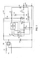
- FIG. 1 illustrates an LED lamp driver circuit 100 including a bridge rectifier D1, a LED controller 110 and a converter circuit 120.
- the LED lamp driver circuit may include different and/or additional components than those shown in FIG. 1 .
- converter circuit 120 senses and provides a voltage to the LED controller 110. Using the sensed voltage to control operation of the converter circuit 120 reduces the cost and complexity of the converter circuit 120 while mitigating power loss caused by current sensing.
- converter circuit 120 comprises resistors R2, R5 and R6, inductor L1, diodes D2 and D4, and capacitors C6 and C9. Additionally, switch Q1 is coupled to the output of the diode bridge D1 and to the converter circuit 120. Switch Q1 receives a control signal from the LED controller 110 and regulates a connection of the converter circuit 120 to the output of the diode bridge D1 accordingly.
- switch Q1 when the control signal has a high value, switch Q1 is in an on state where the rectified input voltage from the output of the diode bridge D1 is coupled to the converter circuit 120; conversely, when the control signal has a low value, switch Q1 is in an off state where the rectified input voltage from the output of the diode bridgeD1 is not coupled to the converter circuit 120.
- switch Q1 may be a bipolar junction transistor (BJT) or a metal oxide semiconductor field effect transistor (MOSFET).
- Inductor L1 stores power from rectified input voltage when switch Q1 is in the on state and releases stored power when switch Q1 is in an off state.
- Resistors R5 and R6 form a voltage divider providing a sensed voltage across inductor L1, "the sensed inductor voltage," to the LED controller 110. From the sensed inductor voltage, the LED controller 110 generates a regulation voltage used to generate the control signal for operating switch Q1, as further described below.
- the LED controller 110 controls converter circuit 120 to achieve constant current operation in which substantially constant current is maintained through LED lamps coupled to the LED driver circuit 100.
- the LED controller 110 maintains constant current operation by estimating output current of the converter circuit 120 from an inductor reset time obtained from the sensed inductor voltage, the length of time switch Q1 is in an on-state and the length of time between switch Q1 being in on-states, as further described below.
- the LED controller 110 receives sensed voltage input to the converter circuit 120, measured across a sensing resistor (resistor R is in FIG. 2 ) and sensed inductor voltage V L from the converter circuit 120. Based on the sensed inductor voltage V L and the sensed input voltage V Ris , the LED controller 110 generates a control signal modifying the state of a switch providing input voltage to the converter circuit 120. Hence, the LED controller 110 regulates the current output by the converter circuit 120. Additionally, by controlling supply of input voltage to the converter circuit 120, the LED controller 110 prevents the output of the converter circuit 120 from overshooting, protecting LED lamps coupled to the LED driver circuit 100.
- FIG. 2 illustrates an example embodiment of an LED controller 110 including a regulation voltage generator 210, a digital-to-analog converter (DAC) 220, a comparator 230 and a pulse width modulation (PWM) unit 240.
- An output of the LED controller 110 is coupled to a switch 250, which is coupled to an input voltage Vin as well as to an input sensing resistor R is .
- FIG. 2 also illustrates components of the converter circuit coupled to the input sensing resistor R is for purposes of illustration.
- the regulation voltage generator 210 generates a regulation voltage based on an inductor voltage V L from a voltage divider, formed by R5 and R6, in parallel to the inductor L1 in the converter circuit, data specifying the length of time time during which the switch 250 is on, T on , and the switching period, T p , of the switch 250.
- the switching period, T p is length of time between the switch entering an on state and again entering an on state. For example, T p is the length of time between the rising edges of a control signal applied to the switch 250.
- the regulation voltage generator 210 uses the inductor voltage V L , T on and T p , the regulation voltage generator 210 generates regulation voltage used to generate one or more control signals for the switch 250.
- the regulation voltage generated by the regulation voltage generator 210 is a digital value that is communicated to the DAC 220, which produces an analog regulation voltage V reg .
- the regulation voltage generator 210 uses the inductor voltage V L to determine a reset time, T rst , for the inductor L1. For example, the regulation voltage generator 210 receives the inductor voltage V L during operation and determines the reset time, T rst , as the time needed for the inductor voltage V L to transition from a first voltage level to a second voltage level. For example, the regulation voltage generator 210 determines T rst as the time for the inductor voltage V L to transition from a voltage of V o -V in to a voltage of V o , where V in is an input voltage to the converter circuit and V o is an output voltage of the converter circuit.
- V reg 2 ⁇ I out ⁇ R is ⁇ T p T on + T rst
- K cc may be determined as double the product of the specified output current I out and the resistance of the current sense resistor R is . From the stored constant, K cc , switch on time, T ON , of the switch 250 and switch period, T p , of the switch 250 and the inductor reset time, T rst .
- the DAC 220 outputs an analog version of the regulation voltage V reg as an input to the comparator 230, which also receives the voltage across the input sensing resistor V Ris as input.
- the comparator 230 determines whether the voltage across the current sense resistor V Ris exceeds the regulation voltage V reg and generates a control signal T on_cc based on the determination. If the voltage across the input sensing resistor V Ris exceeds the regulation voltage V reg , the control signal T on_cc has a first value that terminates the on state of the switch 250.
- the control signal T on_cc is communicated to the PWM unit 240 which modifies the state of the switch 250 accordingly.
- the PWM unit modifies the switch 250 to terminate the on state.
- the LED controller 310 determines a regulation voltage V reg from the inductor voltage V L and uses the regulation voltage V reg to produce a control signal modifying the state of the switch 250.
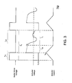
- FIG.3 illustrates example waveforms produced by the LED controller 110 illustrated in FIG. 2 .
- FIG. 3 shows the control signal applied to the switch 250 by the LED controller 110 to transition it between an on state and an off state.
- the switch is in an on state when the control signal is high and is in an off state when the control signal is low.
- the switch 250 is in the on state for the time the control signal is high, identified in FIG. 3 as T on .
- T off the switch 250 is in an off state.
- FIG. 3 also identifies the time between the control signal rising to a high level and the control signal again rising to the high level as the switching period, denoted as T p .
- the inductor voltage V L is the difference between the input voltage V in and the output voltage V o , denoted as V o -V in in FIG. 3 .
- the inductor voltage V L is V o .
- FIG. 3 also shows the inductor current, illustrating that the inductor current has a triangular waveform increasing from zero to a maximum value I max while the switch 250 is in the on state.
- the inductor current is maximized at the end of the interval when the control signal is high.
- the switch 250 enters an off state, and the inductor current decreases from the maximum value I max back to zero over a time interval, which is the reset time T rst .
- the reset time T rst also corresponds to the time elapsed for the inductor voltage to reach the output voltage V o .
- the LED controller 110 may determine the reset time T rst by monitoring the inductor voltage V L and calculating the time for the inductor voltage V L to reach the output voltage V o when the switch 250 transitions from the on state to the off state.
- FIG. 3 also shows the presence of dead time T d during the time the control signal is low. During the dead time T d , the inductor voltage V L continues to decrease from the output voltage Vo and the inductor current is zero.
- the switch 250 When the control signal transitions to a high state, the switch 250 again transitions to an on state, the inductor voltage V L transitions to the output voltage less the input voltage V o -V in and the inductor current begins linearly rising from zero to its maximum value I pk . The inductor current reaches its maximum value I pk when the switch 250 transitions to the off state. When the switch 250 transitions to the off state, the inductor current begins linearly decreasing from its maximum value I pk to zero during the reset time T rst .
- the inductor voltage V L transitions to the output voltage V o , reaching the output voltage V o at the end of the reset time T rst , when the inductor currents returns to having a value of zero.
Landscapes
- Circuit Arrangement For Electric Light Sources In General (AREA)
- Dc-Dc Converters (AREA)
Abstract
Description
- The present invention relates to driving LED (Light-Emitting Diode) lamps and, more specifically, to controlling the current supplied to the LED lamps.
- LEDs are being adopted in a wide variety of electronics applications, for example, architectural lighting, automotive head and tail lights, backlights for liquid crystal display devices, flashlights, etc. Compared to conventional lighting sources such as incandescent lamps and fluorescent lamps, LEDs have significant advantages, including high power efficiency, good directionality, color stability, high reliability, long life time, small size, and environmental safety. Because of advantages over incandescent lamps, particularly the power efficiency (lumens per watt) and spectral quality, use of LED lamps rather than incandescent lamps is expected to increase. Additionally, LED lamps have lower environmental impact than fluorescent lighting systems (fluorescent ballast combined with fluorescent lamp), which that may cause mercury contamination during fluorescent lamp disposal.
- However, while conventional incandescent lighting systems are voltage driven devices, LED lamps are current-driven devices. Hence, conventional LED lamps cannot be direct replacements of incandescent lamps and fluorescent systems without modifications to current wiring and component infrastructure. Because LED lamps are current driven, different techniques for controlling them are required.
- Conventional techniques for regulating current used to drive LED lamps use an output current sensing resistor or a transformer. However, use of an output current sensing resistor causes power loss, while use of a current transformer increases overall system cost. Additionally, conventional techniques monitor the current driving a LED lamp and the output voltage to prevent voltage overshoot and protect the LED lamp by using a separate sets of components, further increasing system complexity.
- A light emitting diode (LED) controller provides constant current regulation for a converter circuit providing current to an LED. The LED controller senses an inductor voltage and determines an inductor reset time from the sensed inductor voltage. Based on the determined inductor reset time, a switching on time and a switching period, the LED controller generates a control signal modifying the state of a switch coupling the converter circuit to an input voltage.
- The features and advantages described in the specification are not all inclusive and, in particular, many additional features and advantages will be apparent to one of ordinary skill in the art in view of the drawings and specification. Moreover, it should be noted that the language used in the specification has been principally selected for readability and instructional purposes, and may not have been selected to delineate or circumscribe the inventive subject matter.
- The teachings of the present invention can be readily understood by considering the following detailed description in conjunction with the accompanying drawings.
-
FIG. 1 illustrates a light emitting diode (LED) lamp driver circuit according to one embodiment of the present invention. -
FIG. 2 illustrates a block diagram of a LED controller providing constant current without using output current sense resistor or current transformer according to one embodiment of the present invention. -
FIG.3 illustrates example waveforms produced by the LED controller illustrated inFIG. 2 according to one embodiment. - The Figures (FIGS.) and the following description relate to preferred embodiments of the present invention by way of illustration only. It should be noted that from the following discussion, alternative embodiments of the structures and methods disclosed herein will be readily recognized as viable alternatives that may be employed without departing from the principles of the claimed invention.
- Reference will now be made in detail to several embodiments of the present invention(s), examples of which are illustrated in the accompanying Figures. It is noted that wherever practicable similar or like reference numbers may be used in the Figures and may indicate similar or like functionality. The Figures depict embodiments of the present invention for purposes of illustration only. One skilled in the art will readily recognize from the following description that alternative embodiments of the structures and methods illustrated herein may be employed without departing from the principles of the invention described herein.
-
FIG. 1 illustrates an LEDlamp driver circuit 100 including a bridge rectifier D1, aLED controller 110 and aconverter circuit 120. In other embodiments, the LED lamp driver circuit may include different and/or additional components than those shown inFIG. 1 . - Bridge rectifier D1 generates a rectified input voltage from an input voltage Vin. Converter circuit 120 generates a direct current (DC) voltage from the rectified input voltage and is controlled by a control signal from the
LED controller 110. In one embodiment,converter circuit 120 is a boost converter generating a DC boosted voltage output that is greater than its input voltage. In another embodiment,converter circuit 120 is a buck converter generating a DC voltage less than the input voltage. Alternatively, theconverter circuit 120 is a buck-boost converter capable of producing an output voltage that may be greater than or less than its input voltage. Theconverter circuit 120 also provides a sensed inductor voltage to theLED controller 110, which theLED controller 110 uses to generate the control signal for a switch Q1 regulating the input voltage to theconverter circuit 120. Unlike conventional converter circuits, which sense and provide both a current and a voltage to aLED controller 110,converter circuit 120 senses and provides a voltage to theLED controller 110. Using the sensed voltage to control operation of theconverter circuit 120 reduces the cost and complexity of theconverter circuit 120 while mitigating power loss caused by current sensing. - In one embodiment,
converter circuit 120 comprises resistors R2, R5 and R6, inductor L1, diodes D2 and D4, and capacitors C6 and C9. Additionally, switch Q1 is coupled to the output of the diode bridge D1 and to theconverter circuit 120. Switch Q1 receives a control signal from theLED controller 110 and regulates a connection of theconverter circuit 120 to the output of the diode bridge D1 accordingly. For example, when the control signal has a high value, switch Q1 is in an on state where the rectified input voltage from the output of the diode bridge D1 is coupled to theconverter circuit 120; conversely, when the control signal has a low value, switch Q1 is in an off state where the rectified input voltage from the output of the diode bridgeD1 is not coupled to theconverter circuit 120. In various embodiments, switch Q1 may be a bipolar junction transistor (BJT) or a metal oxide semiconductor field effect transistor (MOSFET). - Inductor L1 stores power from rectified input voltage when switch Q1 is in the on state and releases stored power when switch Q1 is in an off state. Resistors R5 and R6 form a voltage divider providing a sensed voltage across inductor L1, "the sensed inductor voltage," to the
LED controller 110. From the sensed inductor voltage, theLED controller 110 generates a regulation voltage used to generate the control signal for operating switch Q1, as further described below. In one embodiment, theLED controller 110controls converter circuit 120 to achieve constant current operation in which substantially constant current is maintained through LED lamps coupled to theLED driver circuit 100. In one embodiment, theLED controller 110 maintains constant current operation by estimating output current of theconverter circuit 120 from an inductor reset time obtained from the sensed inductor voltage, the length of time switch Q1 is in an on-state and the length of time between switch Q1 being in on-states, as further described below. - The
LED controller 110 receives sensed voltage input to theconverter circuit 120, measured across a sensing resistor (resistor Ris inFIG. 2 ) and sensed inductor voltage VL from theconverter circuit 120. Based on the sensed inductor voltage VL and the sensed input voltage VRis, theLED controller 110 generates a control signal modifying the state of a switch providing input voltage to theconverter circuit 120. Hence, theLED controller 110 regulates the current output by theconverter circuit 120. Additionally, by controlling supply of input voltage to theconverter circuit 120, theLED controller 110 prevents the output of theconverter circuit 120 from overshooting, protecting LED lamps coupled to theLED driver circuit 100. -
FIG. 2 illustrates an example embodiment of anLED controller 110 including aregulation voltage generator 210, a digital-to-analog converter (DAC) 220, acomparator 230 and a pulse width modulation (PWM)unit 240. An output of theLED controller 110 is coupled to aswitch 250, which is coupled to an input voltage Vin as well as to an input sensing resistor Ris.FIG. 2 also illustrates components of the converter circuit coupled to the input sensing resistor Ris for purposes of illustration. - The
regulation voltage generator 210 generates a regulation voltage based on an inductor voltage VL from a voltage divider, formed by R5 and R6, in parallel to the inductor L1 in the converter circuit, data specifying the length of time time during which theswitch 250 is on, Ton, and the switching period, Tp, of theswitch 250. The switching period, Tp, is length of time between the switch entering an on state and again entering an on state. For example, Tp is the length of time between the rising edges of a control signal applied to theswitch 250. Using the inductor voltage VL, Ton and Tp, theregulation voltage generator 210 generates regulation voltage used to generate one or more control signals for theswitch 250. In one embodiment, the regulation voltage generated by theregulation voltage generator 210 is a digital value that is communicated to theDAC 220, which produces an analog regulation voltage Vreg. - To generate the regulation voltage, the
regulation voltage generator 210 uses the inductor voltage VL to determine a reset time, Trst, for the inductor L1. For example, theregulation voltage generator 210 receives the inductor voltage VL during operation and determines the reset time, Trst, as the time needed for the inductor voltage VL to transition from a first voltage level to a second voltage level. For example, theregulation voltage generator 210 determines Trst as the time for the inductor voltage VL to transition from a voltage of Vo -Vin to a voltage of Vo, where Vin is an input voltage to the converter circuit and Vo is an output voltage of the converter circuit. In one embodiment, theregulation voltage generator 210 calculates the regulation voltage as:
where Kcc is a constant further described below, Tp is the switching period of theswitch 250, Ton is the time the switch 260 is in an on state and Trst is the reset time of the inductor L1. In one embodiment, thevoltage regulation generator 210 calculates Kcc as:
where Ris_nom is the resistance of the input sensing resistor Ris, which may be specified or predetermined, and Iout_nom, also identified as Ioux, is the specified, or desired, output current for the converter circuit. Based on Ris_nom and Iout_nom Kcc may be determined from the constant output current regulation theory, which provides:
- The peak current, ipk, can be expressed in terms of the voltage across the input sensing resistor Ris as ipk = Vreg/Ris. Substituting this in Equation (3) and solving for Vreg results in:

- Accordingly, Kcc may be determined as double the product of the specified output current Iout and the resistance of the current sense resistor Ris. From the stored constant, Kcc, switch on time, TON, of the
switch 250 and switch period, Tp, of theswitch 250 and the inductor reset time, Trst. - The
DAC 220 outputs an analog version of the regulation voltage Vreg as an input to thecomparator 230, which also receives the voltage across the input sensing resistor VRis as input. Thecomparator 230 determines whether the voltage across the current sense resistor VRis exceeds the regulation voltage Vreg and generates a control signal Ton_cc based on the determination. If the voltage across the input sensing resistor VRis exceeds the regulation voltage Vreg, the control signal Ton_cc has a first value that terminates the on state of theswitch 250. The control signal Ton_cc is communicated to thePWM unit 240 which modifies the state of theswitch 250 accordingly. For example, if the control signal Ton_cc has the first value, the PWM unit modifies theswitch 250 to terminate the on state. Hence, the LED controller 310 determines a regulation voltage Vreg from the inductor voltage VL and uses the regulation voltage Vreg to produce a control signal modifying the state of theswitch 250. -
FIG.3 illustrates example waveforms produced by theLED controller 110 illustrated inFIG. 2 .FIG. 3 shows the control signal applied to theswitch 250 by theLED controller 110 to transition it between an on state and an off state. InFIG. 3 , the switch is in an on state when the control signal is high and is in an off state when the control signal is low. Hence, inFIG. 3 , theswitch 250 is in the on state for the time the control signal is high, identified inFIG. 3 as Ton. During the time the control signal is low Toff theswitch 250 is in an off state.FIG. 3 also identifies the time between the control signal rising to a high level and the control signal again rising to the high level as the switching period, denoted as Tp. - In the example of
FIG. 3 , during Ton, when theswitch 250 is in an on state, the inductor voltage VL is the difference between the input voltage Vin and the output voltage Vo, denoted as Vo -Vin inFIG. 3 . However, when theswitch 250 is in an off state, the inductor voltage VL is Vo, -
FIG. 3 also shows the inductor current, illustrating that the inductor current has a triangular waveform increasing from zero to a maximum value Imax while theswitch 250 is in the on state. Thus, the inductor current is maximized at the end of the interval when the control signal is high. When the control signal transitions from a high level to a low level, theswitch 250 enters an off state, and the inductor current decreases from the maximum value Imax back to zero over a time interval, which is the reset time Trst. As shown inFIG. 3 , the reset time Trst also corresponds to the time elapsed for the inductor voltage to reach the output voltage Vo. Hence, theLED controller 110 may determine the reset time Trst by monitoring the inductor voltage VL and calculating the time for the inductor voltage VL to reach the output voltage Vo when theswitch 250 transitions from the on state to the off state.FIG. 3 also shows the presence of dead time Td during the time the control signal is low. During the dead time Td, the inductor voltage VL continues to decrease from the output voltage Vo and the inductor current is zero. - When the control signal transitions to a high state, the
switch 250 again transitions to an on state, the inductor voltage VL transitions to the output voltage less the input voltage Vo -Vin and the inductor current begins linearly rising from zero to its maximum value Ipk. The inductor current reaches its maximum value Ipk when theswitch 250 transitions to the off state. When theswitch 250 transitions to the off state, the inductor current begins linearly decreasing from its maximum value Ipk to zero during the reset time Trst. Also during the reset time Trst, the inductor voltage VL transitions to the output voltage Vo, reaching the output voltage Vo at the end of the reset time Trst, when the inductor currents returns to having a value of zero. - Upon reading this disclosure, those of skill in the art will appreciate still additional alternative designs for LED controllers providing constant current control without current sensing. Thus, while particular embodiments and applications of the present invention have been illustrated and described, it is to be understood that the invention is not limited to the precise construction and components disclosed herein and that various modifications, changes and variations which will be apparent to those skilled in the art may be made in the arrangement, operation and details of the method and apparatus of the present invention disclosed herein without departing from the scope of the invention.
Claims (15)
- A method for limiting an output current of a power supply, an output of the power supply coupled to an inductor, the method comprising:sensing a voltage across the inductor;sensing a voltage across a switching current sense resistor coupled to a switch and to the inductor;determining a reset time of the inductor using the voltage across the inductor, the reset time representing a duration for a current across the inductor to decrease from a peak value to a minimum value;determining a regulation voltage from the reset time, a period of the switch and a length of time the switch is in an on state;generating a control signal responsive to a comparison between the voltage across the switching current sense resistor and the regulation voltage, the control signal transitioning the switch to an off state responsive to the voltage across the switching current sense resistor exceeding the regulation voltage.
- The method of claim 1, wherein the regulation voltage is directly proportional to the period of the switch and inversely proportional to the sum of the reset time and the length of time the switch is in an on state.
- The method of claim 2, wherein the regulation voltage is directly proportional to a nominal output current value and a resistance of the switching current sense resistor.
- The method of claim 1, wherein generating the control signal comprises determining the duty cycle of the control signal based on the comparison between the voltage across the switching current sense resistor and the regulation voltage.
- The method of claim 1 further comprising:charging the inductor responsive to the switch being in an on state; anddischarging the inductor responsive to the switch being in an off state.
- The method of claim 5, wherein the inductor discharges through a light emitting diode (LED).
- A constant current controller comprising:a converter circuit, comprising:a switch configured to turn on or off responsive to a switch input voltage being active or inactive, andan inductor coupled to the switch configured to store power from a supply voltage when the switch is on and to transfer power to a load when the switch is off;a voltage sense coupled to the inductor of the converter circuit, the voltage sense configured to sense an inductor voltage across the inductor; anda controller comprising a first input coupled to the voltage sense and an output coupled to the switch of the converter circuit, the controller configured to receive the sensed inductor voltage from the voltage sense and generate the switch input voltage to turn the switch on or off based on the received sensed inductor voltage.
- The constant current controller of claim 7 further comprising a switching current sense resistor coupled to the switch of the converter circuit and to the inductor of the converter circuit, the switching current sense resistor configured to sense the current through the switch during the switch on time.
- The constant current controller of claim 8, wherein the controller comprises:a regulation voltage generator coupled to the first input of the controller, the regulation voltage generator configured to generate a regulation voltage based on the sensed inductor voltage, a length of time the switch of the converter circuit is on and a period of the switch.a comparator receiving the regulation voltage from the regulation voltage generator and the voltage across the switching current sense resistor, the comparator configured to generate a comparator output signal responsive to a comparison between the regulation voltage and the voltage across the switching current sense resistor.a pulse width modulator (PWM) configured to receive the comparator output signal and generate a control signal transitioning the switch to an off state responsive to the voltage across the switching current sense resistor exceeding the regulation voltage.
- The constant current controller of claim 9, wherein the regulation voltage is directly proportional to the period of the switch and inversely proportional to the sum of a reset time and the length of time the switch of the converter circuit is on, the reset time representing a duration for a current across the inductor of the converter circuit to decrease from a peak value to a minimum value.
- The constant current controller of claim 10, wherein the regulation voltage is directly proportional to a nominal output current value and a resistance of the switching current sense resistor.
- The constant current controller of claim 8 wherein the controller further comprises a digital to analog converter (DAC), an input of the DAC coupled to the output of the regulation voltage generator and an output of the DAC coupled to the comparator, the DAC configured to convert a digital representation of the regulation voltage into an analog representation of the regulation voltage.
- The constant current controller of claim 11 further comprising a bridge rectifier coupled to the switch, the bridge rectifier configured to rectify an alternating current (AC) supply voltage and generate a direct current (DC) supply voltage.
- The constant current controller of claim 7 wherein the switch is one of a bipolar junction transistor (BJT) and a field effect transistor (FET) such as a metal oxide semiconductor FET (MOSFET).
- The constant current controller of claim 7 wherein the load is a light emitting diode (LED).
Applications Claiming Priority (2)
| Application Number | Priority Date | Filing Date | Title |
|---|---|---|---|
| US201261648444P | 2012-05-17 | 2012-05-17 | |
| US13/891,163 US9420645B2 (en) | 2012-05-17 | 2013-05-09 | Constant current control buck converter without current sense |
Publications (2)
| Publication Number | Publication Date |
|---|---|
| EP2672784A1 true EP2672784A1 (en) | 2013-12-11 |
| EP2672784B1 EP2672784B1 (en) | 2016-07-20 |
Family
ID=48463767
Family Applications (1)
| Application Number | Title | Priority Date | Filing Date |
|---|---|---|---|
| EP13167870.8A Active EP2672784B1 (en) | 2012-05-17 | 2013-05-15 | Constant current control buck converter without current sense |
Country Status (4)
| Country | Link |
|---|---|
| US (1) | US9420645B2 (en) |
| EP (1) | EP2672784B1 (en) |
| CN (1) | CN103427642B (en) |
| TW (1) | TWI509963B (en) |
Families Citing this family (7)
| Publication number | Priority date | Publication date | Assignee | Title |
|---|---|---|---|---|
| US9214862B2 (en) * | 2014-04-17 | 2015-12-15 | Philips International, B.V. | Systems and methods for valley switching in a switching power converter |
| CN105722283A (en) * | 2014-12-02 | 2016-06-29 | 中兴通讯股份有限公司 | Current-type LCD backlight boosting method and current-type LCD backlight boosting circuit |
| US10523116B2 (en) * | 2018-03-30 | 2019-12-31 | Texas Instruments Incorporated | Timer for creating a stable on time |
| CN111416519B (en) * | 2020-05-07 | 2021-06-22 | 矽力杰半导体技术(杭州)有限公司 | Inductor current reconstruction circuit, reconstruction method and power converter using the same |
| KR102650608B1 (en) * | 2020-12-18 | 2024-03-25 | 세메스 주식회사 | Light processing member, substrate processing apparatus including the same and substrate processing method |
| US12362537B2 (en) * | 2021-08-13 | 2025-07-15 | Lumentum Operations Llc | Driver circuit for evaluation of an optical emitter |
| US12040692B2 (en) | 2022-06-02 | 2024-07-16 | Murata Manufacturing Co., Ltd. | Circuits and methods for generating a continuous current sense signal |
Citations (6)
| Publication number | Priority date | Publication date | Assignee | Title |
|---|---|---|---|---|
| US20050276294A1 (en) * | 2004-06-09 | 2005-12-15 | Crawford Ian D | Polyphase diode driver |
| US20080112193A1 (en) * | 2006-11-09 | 2008-05-15 | Iwatt Inc. | On-Time Control For Constant Current Mode In A Flyback Power Supply |
| US20090059632A1 (en) * | 2007-08-28 | 2009-03-05 | Yong Li | System And Method For Controlling A Current Limit With Primary Side Sensing Using A Hybrid PWM and PFM Control |
| US20090058323A1 (en) * | 2007-08-30 | 2009-03-05 | Ta-Yung Yang | Flyback LED drive circuit with constant current regulation |
| JP2011223800A (en) * | 2010-04-13 | 2011-11-04 | Minebea Co Ltd | Switching power supply circuit |
| US20120025736A1 (en) * | 2010-07-30 | 2012-02-02 | Rahul Singh | Integrated circuit switching power supply controller with selectable buck mode operation |
Family Cites Families (10)
| Publication number | Priority date | Publication date | Assignee | Title |
|---|---|---|---|---|
| US7285919B2 (en) * | 2001-06-22 | 2007-10-23 | Lutron Electronics Co., Inc. | Electronic ballast having improved power factor and total harmonic distortion |
| AU2002354249A1 (en) | 2001-11-29 | 2003-06-10 | Iwatt | Power converters with primary-only feedback |
| US6862194B2 (en) | 2003-06-18 | 2005-03-01 | System General Corp. | Flyback power converter having a constant voltage and a constant current output under primary-side PWM control |
| US7054170B2 (en) | 2004-01-05 | 2006-05-30 | System General Corp. | Power-mode controlled power converter |
| US7362593B2 (en) | 2004-09-16 | 2008-04-22 | System General Corp. | Switching control circuit having off-time modulation to improve efficiency of primary-side controlled power supply |
| ITTO20070859A1 (en) | 2007-11-29 | 2009-05-30 | St Microelectronics Srl | VOLTAGE ISOLATED CONVERTER WITH FEEDBACK TO THE PRIMARY, AND RELATIVE OUTPUT TENSION CONTROL METHOD |
| CN101997412B (en) | 2009-08-19 | 2013-06-26 | 通嘉科技股份有限公司 | Control Method |
| CN101841242B (en) | 2010-04-14 | 2012-11-21 | 上海明石光电科技有限公司 | Switch power supply and method for adjusting output current thereof |
| US8432109B2 (en) | 2010-10-01 | 2013-04-30 | System General Corp. | Method and apparatus for a LED driver with high power factor |
| CN102035415B (en) | 2010-12-24 | 2013-02-27 | 常州博拓电子科技有限公司 | Constant-current implementation method for isolated AC/DC switched power supply for LED illumination drive and special device thereof |
-
2013
- 2013-05-09 US US13/891,163 patent/US9420645B2/en active Active
- 2013-05-15 EP EP13167870.8A patent/EP2672784B1/en active Active
- 2013-05-17 CN CN201310191501.8A patent/CN103427642B/en active Active
- 2013-05-17 TW TW102117622A patent/TWI509963B/en active
Patent Citations (6)
| Publication number | Priority date | Publication date | Assignee | Title |
|---|---|---|---|---|
| US20050276294A1 (en) * | 2004-06-09 | 2005-12-15 | Crawford Ian D | Polyphase diode driver |
| US20080112193A1 (en) * | 2006-11-09 | 2008-05-15 | Iwatt Inc. | On-Time Control For Constant Current Mode In A Flyback Power Supply |
| US20090059632A1 (en) * | 2007-08-28 | 2009-03-05 | Yong Li | System And Method For Controlling A Current Limit With Primary Side Sensing Using A Hybrid PWM and PFM Control |
| US20090058323A1 (en) * | 2007-08-30 | 2009-03-05 | Ta-Yung Yang | Flyback LED drive circuit with constant current regulation |
| JP2011223800A (en) * | 2010-04-13 | 2011-11-04 | Minebea Co Ltd | Switching power supply circuit |
| US20120025736A1 (en) * | 2010-07-30 | 2012-02-02 | Rahul Singh | Integrated circuit switching power supply controller with selectable buck mode operation |
Non-Patent Citations (1)
| Title |
|---|
| TZUEN-LIH CHERN ET AL: "Single-stage Flyback converter for led driver with inductor voltage detection power factor correction", INDUSTRIAL ELECTRONICS AND APPLICATIONS (ICIEA), 2010 THE 5TH IEEE CONFERENCE ON, IEEE, PISCATAWAY, NJ, USA, 15 June 2010 (2010-06-15), pages 2082 - 2087, XP031712128, ISBN: 978-1-4244-5045-9 * |
Also Published As
| Publication number | Publication date |
|---|---|
| TWI509963B (en) | 2015-11-21 |
| CN103427642B (en) | 2017-04-12 |
| CN103427642A (en) | 2013-12-04 |
| EP2672784B1 (en) | 2016-07-20 |
| TW201401743A (en) | 2014-01-01 |
| US9420645B2 (en) | 2016-08-16 |
| US20130307425A1 (en) | 2013-11-21 |
Similar Documents
| Publication | Publication Date | Title |
|---|---|---|
| US9420645B2 (en) | Constant current control buck converter without current sense | |
| US8995150B2 (en) | Primary side sense output current regulation | |
| KR101240131B1 (en) | System and method for driving a light source | |
| US8508150B2 (en) | Controllers, systems and methods for controlling dimming of light sources | |
| TWI461105B (en) | Dimming controllers, driving circuits and methods for controlling power of light source | |
| EP2515611B1 (en) | Lighting device and illumination apparatus | |
| TWI388115B (en) | Power conversion drive circuit and lamp drive circuit | |
| US8575853B2 (en) | System and method for supplying constant power to luminuous loads | |
| US20100219764A1 (en) | Led dimming apparatus | |
| US9232581B2 (en) | Output current compensation for jitter in input voltage for dimmable LED lamps | |
| EP2498579A2 (en) | Controllers, systems and methods for controlling dimming of light sources | |
| US8049436B2 (en) | Dimmer and lighting apparatus | |
| JP2012216766A (en) | Led drive device and led lighting apparatus | |
| TW201301936A (en) | A cascade boost and inverting buck converter with independent control | |
| EP2706820A2 (en) | Solid-state light-emitting element drive device, lighting system and lighting fixture | |
| CN102695325A (en) | Drive circuit and control circuit | |
| JP2013140931A (en) | Circuits and methods for driving led light sources | |
| JP2006222376A (en) | Power supply device and lighting device | |
| EP3139483A1 (en) | Electronic reverse buck converter, and corresponding method of operating an electronic reverse buck converter | |
| KR101904806B1 (en) | LED Convertor for Constant Power | |
| JP2007073781A (en) | Light emitting diode drive device | |
| GB2513478A (en) | Circuits and methods for driving light sources | |
| US20160156269A1 (en) | Power converter circuitry with switching frequency control circuitry | |
| US9380670B2 (en) | Generating a voltage feedback signal in non-isolated LED drivers | |
| KR101188916B1 (en) | Driver for light source |
Legal Events
| Date | Code | Title | Description |
|---|---|---|---|
| PUAI | Public reference made under article 153(3) epc to a published international application that has entered the european phase |
Free format text: ORIGINAL CODE: 0009012 |
|
| 17P | Request for examination filed |
Effective date: 20130515 |
|
| AK | Designated contracting states |
Kind code of ref document: A1 Designated state(s): AL AT BE BG CH CY CZ DE DK EE ES FI FR GB GR HR HU IE IS IT LI LT LU LV MC MK MT NL NO PL PT RO RS SE SI SK SM TR |
|
| AX | Request for extension of the european patent |
Extension state: BA ME |
|
| RIN1 | Information on inventor provided before grant (corrected) |
Inventor name: YAN, LIANG Inventor name: CHEN, GORDON Inventor name: ZHENG, JUNJIE |
|
| RAP1 | Party data changed (applicant data changed or rights of an application transferred) |
Owner name: DIALOG SEMICONDUCTOR INC. |
|
| RIN1 | Information on inventor provided before grant (corrected) |
Inventor name: ZHENG, JUNJIE Inventor name: CHEN, GORDON Inventor name: YAN, LIANG |
|
| 17Q | First examination report despatched |
Effective date: 20140929 |
|
| GRAP | Despatch of communication of intention to grant a patent |
Free format text: ORIGINAL CODE: EPIDOSNIGR1 |
|
| INTG | Intention to grant announced |
Effective date: 20160212 |
|
| GRAS | Grant fee paid |
Free format text: ORIGINAL CODE: EPIDOSNIGR3 |
|
| GRAA | (expected) grant |
Free format text: ORIGINAL CODE: 0009210 |
|
| AK | Designated contracting states |
Kind code of ref document: B1 Designated state(s): AL AT BE BG CH CY CZ DE DK EE ES FI FR GB GR HR HU IE IS IT LI LT LU LV MC MK MT NL NO PL PT RO RS SE SI SK SM TR |
|
| REG | Reference to a national code |
Ref country code: GB Ref legal event code: FG4D |
|
| REG | Reference to a national code |
Ref country code: CH Ref legal event code: EP |
|
| REG | Reference to a national code |
Ref country code: IE Ref legal event code: FG4D |
|
| REG | Reference to a national code |
Ref country code: AT Ref legal event code: REF Ref document number: 814988 Country of ref document: AT Kind code of ref document: T Effective date: 20160815 |
|
| REG | Reference to a national code |
Ref country code: DE Ref legal event code: R096 Ref document number: 602013009510 Country of ref document: DE |
|
| REG | Reference to a national code |
Ref country code: LT Ref legal event code: MG4D |
|
| REG | Reference to a national code |
Ref country code: NL Ref legal event code: MP Effective date: 20160720 |
|
| REG | Reference to a national code |
Ref country code: AT Ref legal event code: MK05 Ref document number: 814988 Country of ref document: AT Kind code of ref document: T Effective date: 20160720 |
|
| PG25 | Lapsed in a contracting state [announced via postgrant information from national office to epo] |
Ref country code: RS Free format text: LAPSE BECAUSE OF FAILURE TO SUBMIT A TRANSLATION OF THE DESCRIPTION OR TO PAY THE FEE WITHIN THE PRESCRIBED TIME-LIMIT Effective date: 20160720 Ref country code: FI Free format text: LAPSE BECAUSE OF FAILURE TO SUBMIT A TRANSLATION OF THE DESCRIPTION OR TO PAY THE FEE WITHIN THE PRESCRIBED TIME-LIMIT Effective date: 20160720 Ref country code: LT Free format text: LAPSE BECAUSE OF FAILURE TO SUBMIT A TRANSLATION OF THE DESCRIPTION OR TO PAY THE FEE WITHIN THE PRESCRIBED TIME-LIMIT Effective date: 20160720 Ref country code: NO Free format text: LAPSE BECAUSE OF FAILURE TO SUBMIT A TRANSLATION OF THE DESCRIPTION OR TO PAY THE FEE WITHIN THE PRESCRIBED TIME-LIMIT Effective date: 20161020 Ref country code: IT Free format text: LAPSE BECAUSE OF FAILURE TO SUBMIT A TRANSLATION OF THE DESCRIPTION OR TO PAY THE FEE WITHIN THE PRESCRIBED TIME-LIMIT Effective date: 20160720 Ref country code: HR Free format text: LAPSE BECAUSE OF FAILURE TO SUBMIT A TRANSLATION OF THE DESCRIPTION OR TO PAY THE FEE WITHIN THE PRESCRIBED TIME-LIMIT Effective date: 20160720 Ref country code: IS Free format text: LAPSE BECAUSE OF FAILURE TO SUBMIT A TRANSLATION OF THE DESCRIPTION OR TO PAY THE FEE WITHIN THE PRESCRIBED TIME-LIMIT Effective date: 20161120 Ref country code: NL Free format text: LAPSE BECAUSE OF FAILURE TO SUBMIT A TRANSLATION OF THE DESCRIPTION OR TO PAY THE FEE WITHIN THE PRESCRIBED TIME-LIMIT Effective date: 20160720 |
|
| PG25 | Lapsed in a contracting state [announced via postgrant information from national office to epo] |
Ref country code: PL Free format text: LAPSE BECAUSE OF FAILURE TO SUBMIT A TRANSLATION OF THE DESCRIPTION OR TO PAY THE FEE WITHIN THE PRESCRIBED TIME-LIMIT Effective date: 20160720 Ref country code: SE Free format text: LAPSE BECAUSE OF FAILURE TO SUBMIT A TRANSLATION OF THE DESCRIPTION OR TO PAY THE FEE WITHIN THE PRESCRIBED TIME-LIMIT Effective date: 20160720 Ref country code: GR Free format text: LAPSE BECAUSE OF FAILURE TO SUBMIT A TRANSLATION OF THE DESCRIPTION OR TO PAY THE FEE WITHIN THE PRESCRIBED TIME-LIMIT Effective date: 20161021 Ref country code: ES Free format text: LAPSE BECAUSE OF FAILURE TO SUBMIT A TRANSLATION OF THE DESCRIPTION OR TO PAY THE FEE WITHIN THE PRESCRIBED TIME-LIMIT Effective date: 20160720 Ref country code: AT Free format text: LAPSE BECAUSE OF FAILURE TO SUBMIT A TRANSLATION OF THE DESCRIPTION OR TO PAY THE FEE WITHIN THE PRESCRIBED TIME-LIMIT Effective date: 20160720 Ref country code: PT Free format text: LAPSE BECAUSE OF FAILURE TO SUBMIT A TRANSLATION OF THE DESCRIPTION OR TO PAY THE FEE WITHIN THE PRESCRIBED TIME-LIMIT Effective date: 20161121 Ref country code: BE Free format text: LAPSE BECAUSE OF FAILURE TO SUBMIT A TRANSLATION OF THE DESCRIPTION OR TO PAY THE FEE WITHIN THE PRESCRIBED TIME-LIMIT Effective date: 20160720 Ref country code: LV Free format text: LAPSE BECAUSE OF FAILURE TO SUBMIT A TRANSLATION OF THE DESCRIPTION OR TO PAY THE FEE WITHIN THE PRESCRIBED TIME-LIMIT Effective date: 20160720 |
|
| REG | Reference to a national code |
Ref country code: DE Ref legal event code: R097 Ref document number: 602013009510 Country of ref document: DE |
|
| PG25 | Lapsed in a contracting state [announced via postgrant information from national office to epo] |
Ref country code: EE Free format text: LAPSE BECAUSE OF FAILURE TO SUBMIT A TRANSLATION OF THE DESCRIPTION OR TO PAY THE FEE WITHIN THE PRESCRIBED TIME-LIMIT Effective date: 20160720 Ref country code: RO Free format text: LAPSE BECAUSE OF FAILURE TO SUBMIT A TRANSLATION OF THE DESCRIPTION OR TO PAY THE FEE WITHIN THE PRESCRIBED TIME-LIMIT Effective date: 20160720 |
|
| PLBE | No opposition filed within time limit |
Free format text: ORIGINAL CODE: 0009261 |
|
| STAA | Information on the status of an ep patent application or granted ep patent |
Free format text: STATUS: NO OPPOSITION FILED WITHIN TIME LIMIT |
|
| PG25 | Lapsed in a contracting state [announced via postgrant information from national office to epo] |
Ref country code: DK Free format text: LAPSE BECAUSE OF FAILURE TO SUBMIT A TRANSLATION OF THE DESCRIPTION OR TO PAY THE FEE WITHIN THE PRESCRIBED TIME-LIMIT Effective date: 20160720 Ref country code: BG Free format text: LAPSE BECAUSE OF FAILURE TO SUBMIT A TRANSLATION OF THE DESCRIPTION OR TO PAY THE FEE WITHIN THE PRESCRIBED TIME-LIMIT Effective date: 20161020 Ref country code: SK Free format text: LAPSE BECAUSE OF FAILURE TO SUBMIT A TRANSLATION OF THE DESCRIPTION OR TO PAY THE FEE WITHIN THE PRESCRIBED TIME-LIMIT Effective date: 20160720 Ref country code: CZ Free format text: LAPSE BECAUSE OF FAILURE TO SUBMIT A TRANSLATION OF THE DESCRIPTION OR TO PAY THE FEE WITHIN THE PRESCRIBED TIME-LIMIT Effective date: 20160720 Ref country code: SM Free format text: LAPSE BECAUSE OF FAILURE TO SUBMIT A TRANSLATION OF THE DESCRIPTION OR TO PAY THE FEE WITHIN THE PRESCRIBED TIME-LIMIT Effective date: 20160720 |
|
| 26N | No opposition filed |
Effective date: 20170421 |
|
| PG25 | Lapsed in a contracting state [announced via postgrant information from national office to epo] |
Ref country code: SI Free format text: LAPSE BECAUSE OF FAILURE TO SUBMIT A TRANSLATION OF THE DESCRIPTION OR TO PAY THE FEE WITHIN THE PRESCRIBED TIME-LIMIT Effective date: 20160720 Ref country code: LU Free format text: LAPSE BECAUSE OF NON-PAYMENT OF DUE FEES Effective date: 20170531 |
|
| REG | Reference to a national code |
Ref country code: CH Ref legal event code: PL |
|
| GBPC | Gb: european patent ceased through non-payment of renewal fee |
Effective date: 20170515 |
|
| PG25 | Lapsed in a contracting state [announced via postgrant information from national office to epo] |
Ref country code: MC Free format text: LAPSE BECAUSE OF FAILURE TO SUBMIT A TRANSLATION OF THE DESCRIPTION OR TO PAY THE FEE WITHIN THE PRESCRIBED TIME-LIMIT Effective date: 20160720 |
|
| REG | Reference to a national code |
Ref country code: IE Ref legal event code: MM4A |
|
| PG25 | Lapsed in a contracting state [announced via postgrant information from national office to epo] |
Ref country code: CH Free format text: LAPSE BECAUSE OF NON-PAYMENT OF DUE FEES Effective date: 20170531 Ref country code: LI Free format text: LAPSE BECAUSE OF NON-PAYMENT OF DUE FEES Effective date: 20170531 |
|
| REG | Reference to a national code |
Ref country code: FR Ref legal event code: ST Effective date: 20180131 |
|
| PG25 | Lapsed in a contracting state [announced via postgrant information from national office to epo] |
Ref country code: LU Free format text: LAPSE BECAUSE OF NON-PAYMENT OF DUE FEES Effective date: 20170515 |
|
| PG25 | Lapsed in a contracting state [announced via postgrant information from national office to epo] |
Ref country code: GB Free format text: LAPSE BECAUSE OF NON-PAYMENT OF DUE FEES Effective date: 20170515 Ref country code: IE Free format text: LAPSE BECAUSE OF NON-PAYMENT OF DUE FEES Effective date: 20170515 |
|
| PG25 | Lapsed in a contracting state [announced via postgrant information from national office to epo] |
Ref country code: FR Free format text: LAPSE BECAUSE OF NON-PAYMENT OF DUE FEES Effective date: 20170531 |
|
| PG25 | Lapsed in a contracting state [announced via postgrant information from national office to epo] |
Ref country code: MT Free format text: LAPSE BECAUSE OF NON-PAYMENT OF DUE FEES Effective date: 20170515 |
|
| PG25 | Lapsed in a contracting state [announced via postgrant information from national office to epo] |
Ref country code: AL Free format text: LAPSE BECAUSE OF FAILURE TO SUBMIT A TRANSLATION OF THE DESCRIPTION OR TO PAY THE FEE WITHIN THE PRESCRIBED TIME-LIMIT Effective date: 20160720 |
|
| PG25 | Lapsed in a contracting state [announced via postgrant information from national office to epo] |
Ref country code: HU Free format text: LAPSE BECAUSE OF FAILURE TO SUBMIT A TRANSLATION OF THE DESCRIPTION OR TO PAY THE FEE WITHIN THE PRESCRIBED TIME-LIMIT; INVALID AB INITIO Effective date: 20130515 |
|
| PG25 | Lapsed in a contracting state [announced via postgrant information from national office to epo] |
Ref country code: CY Free format text: LAPSE BECAUSE OF NON-PAYMENT OF DUE FEES Effective date: 20160720 |
|
| REG | Reference to a national code |
Ref country code: DE Ref legal event code: R079 Ref document number: 602013009510 Country of ref document: DE Free format text: PREVIOUS MAIN CLASS: H05B0033080000 Ipc: H05B0045000000 |
|
| PG25 | Lapsed in a contracting state [announced via postgrant information from national office to epo] |
Ref country code: MK Free format text: LAPSE BECAUSE OF FAILURE TO SUBMIT A TRANSLATION OF THE DESCRIPTION OR TO PAY THE FEE WITHIN THE PRESCRIBED TIME-LIMIT Effective date: 20160720 |
|
| PG25 | Lapsed in a contracting state [announced via postgrant information from national office to epo] |
Ref country code: TR Free format text: LAPSE BECAUSE OF FAILURE TO SUBMIT A TRANSLATION OF THE DESCRIPTION OR TO PAY THE FEE WITHIN THE PRESCRIBED TIME-LIMIT Effective date: 20160720 |
|
| PGFP | Annual fee paid to national office [announced via postgrant information from national office to epo] |
Ref country code: DE Payment date: 20250506 Year of fee payment: 13 |