EP2672488A1 - MRAM element having improved data retention and low writing temperature - Google Patents
MRAM element having improved data retention and low writing temperature Download PDFInfo
- Publication number
- EP2672488A1 EP2672488A1 EP20120290196 EP12290196A EP2672488A1 EP 2672488 A1 EP2672488 A1 EP 2672488A1 EP 20120290196 EP20120290196 EP 20120290196 EP 12290196 A EP12290196 A EP 12290196A EP 2672488 A1 EP2672488 A1 EP 2672488A1
- Authority
- EP
- European Patent Office
- Prior art keywords
- layer
- storage
- antiferromagnetic
- temperature
- blocking temperature
- Prior art date
- Legal status (The legal status is an assumption and is not a legal conclusion. Google has not performed a legal analysis and makes no representation as to the accuracy of the status listed.)
- Granted
Links
Images


Classifications
-
- H—ELECTRICITY
- H10—SEMICONDUCTOR DEVICES; ELECTRIC SOLID-STATE DEVICES NOT OTHERWISE PROVIDED FOR
- H10N—ELECTRIC SOLID-STATE DEVICES NOT OTHERWISE PROVIDED FOR
- H10N50/00—Galvanomagnetic devices
- H10N50/10—Magnetoresistive devices
-
- G—PHYSICS
- G11—INFORMATION STORAGE
- G11C—STATIC STORES
- G11C11/00—Digital stores characterised by the use of particular electric or magnetic storage elements; Storage elements therefor
- G11C11/02—Digital stores characterised by the use of particular electric or magnetic storage elements; Storage elements therefor using magnetic elements
- G11C11/16—Digital stores characterised by the use of particular electric or magnetic storage elements; Storage elements therefor using magnetic elements using elements in which the storage effect is based on magnetic spin effect
-
- G—PHYSICS
- G11—INFORMATION STORAGE
- G11C—STATIC STORES
- G11C11/00—Digital stores characterised by the use of particular electric or magnetic storage elements; Storage elements therefor
- G11C11/02—Digital stores characterised by the use of particular electric or magnetic storage elements; Storage elements therefor using magnetic elements
- G11C11/16—Digital stores characterised by the use of particular electric or magnetic storage elements; Storage elements therefor using magnetic elements using elements in which the storage effect is based on magnetic spin effect
- G11C11/161—Digital stores characterised by the use of particular electric or magnetic storage elements; Storage elements therefor using magnetic elements using elements in which the storage effect is based on magnetic spin effect details concerning the memory cell structure, e.g. the layers of the ferromagnetic memory cell
-
- G—PHYSICS
- G11—INFORMATION STORAGE
- G11C—STATIC STORES
- G11C11/00—Digital stores characterised by the use of particular electric or magnetic storage elements; Storage elements therefor
- G11C11/02—Digital stores characterised by the use of particular electric or magnetic storage elements; Storage elements therefor using magnetic elements
- G11C11/16—Digital stores characterised by the use of particular electric or magnetic storage elements; Storage elements therefor using magnetic elements using elements in which the storage effect is based on magnetic spin effect
- G11C11/165—Auxiliary circuits
- G11C11/1675—Writing or programming circuits or methods
-
- H—ELECTRICITY
- H10—SEMICONDUCTOR DEVICES; ELECTRIC SOLID-STATE DEVICES NOT OTHERWISE PROVIDED FOR
- H10N—ELECTRIC SOLID-STATE DEVICES NOT OTHERWISE PROVIDED FOR
- H10N50/00—Galvanomagnetic devices
- H10N50/80—Constructional details
Definitions
- the present invention concerns a thermally assisted switching MRAM element having improved data retention and low writing mode operating temperature.
- Magnetoresistive random access memory (MRAM) devices are solid state, non-volatile memory devices which make use of the tunnel magnetoresistive effect.
- a conventional MRAM device includes a column of first electrical wires, referred to as word lines, and a row of second electrical wires, referred to as bit lines.
- An array of magnetic memory cells, located at the junctions of the word lines and bit lines, is used to record data signals.
- a typical magnetic memory cell comprises a hard magnetic layer, a soft magnetic layer, and a non-magnetic layer sandwiched between the hard magnetic layer and the soft magnetic layer.
- the hard magnetic layer has a magnetization vector fixed in one direction. The orientation of the magnetization vector does not change under a magnetic field applied thereon.
- the soft magnetic layer has an alterable magnetization vector under a magnetic field applied thereon, that either points to the same direction, hereinafter “parallel allignrnent”, or to the opposite direction, hereinafter “antiparallel alignment", of the magnetization vector of the hard magnetic layer. Since the resistances of the magnetic memory cell in the "parallel alignment” status and the “antiparallel alignment” status are different, the two types of alignment status can be used to record the two logical states, i.e., the "0"s or "1"s of a data bit.
- an electric current passes through the word line and the bit line adjacent to the memory cell.
- a magnetic field generated by the electric current will switch the orientation of the magnetization vector of the soft magnetic layer.
- the magnetization vector of the hard magnetic layer and the soft magnetic layer will be changed from one type of alignment, e.g. "parallel alignment", to the other type of alignment, e.g. "antiparallel alignment”, so that a data signal in form of one data bit can be recorded in the memory cell.
- Patent US5959880 describes an MRAM cell achieving bi-stable switching during the write operation, and good thermal and/or temporal stability of the written data when the ferromagnetic storage layer is made of a material having high magnetocrystalline anisotropy.
- Writing such a MRAM cell require high field currents able to switch the magnetization direction of the ferromagnetic storage layer from a stable logic state to another, resulting in high power consumption.
- a decrease in power consumption can be obtained by reducing the magnetocrystalline anisotropy but at the expense of thermal and temporal stability.
- the above conventional MRAM cells do not simultaneously fulfil low power consumption and thermal and temporal stability.
- the storage layer is pinned by an antiferromagnetic layer, such that the magnetization of the storage layer can be oriented only when the MRAM cell is heated at a high temperature threshold, above a critical temperature of the antiferromagnetic layer.
- TAS-MRAM cell An advantage of the TAS-MRAM cell is that a high selectivity to writing can be achieved by the selective heating of the cell to be written. Moreover, the written data can be maintained when the cell is exposed to parasite magnetic fields at ambient temperature. Another advantage is the possibility of reducing significantly the size of the cell without affecting much the writing stability (or data retention). Reduced power consumption during writing can also be achieved.
- Improving further data retention can be achieved by using an antiferromagnetic layer having a higher critical temperature.
- the high critical temperature antiferromagnetic layer requires heating the MRAM cell at higher temperature and, thus resulting in higher power consumption.
- the present disclosure concerns a MRAM element comprising a magnetic tunnel junction including a reference layer having a reference magnetization; a storage layer having a storage magnetization; a tunnel barrier layer included between the storage layer and the reference layer; and a storage antiferromagnetic layer exchange-coupling the storage layer such as to pin the storage magnetization at a low temperature threshold and to free it at a high temperature threshold; the antiferromagnetic layer comprising at least one first layer having a first storage blocking temperature, and at least one second antiferromagnetic layer having a second storage blocking temperature; the first storage blocking temperature being lower than the second storage blocking temperature.
- the first storage blocking temperature can be below 200°C and the second storage blocking temperature can be above 250°C.
- said at least one first layer can comprise a FeMn-based alloy.
- Said at least one second layer can comprise a Mn-based alloy.
- Said Mn-based alloy can be selected from IrMn, PtMn or NiMn, and preferably a NiMn alloy.
- the antiferromagnetic storage layer can comprise a plurality of the first layer and a plurality of the second layer, each of said plurality of the first antiferromagnetic layer alternating with each of said plurality of the second antiferromagnetic layers.
- the first layer can have a thickness comprised between 0.1 nm and 5 nm and the second layer can have a thickness comprised between 0.1 nm and 5 nm.
- the first layer has a thickness comprised between 0.5 nm and 5 nm and the second layer has a thickness comprised between 0.5 nm and 5 nm.
- the antiferromagnetic storage layer can have a thickness comprised between 5 nm and 50 nm, but preferably between 5 nm and 10 nm.
- the magnetic tunnel junction can further comprise an antiferromagnetic reference layer exchange-coupling the reference layer such as to pin the reference magnetization below a reference blocking temperature of the antiferromagnetic reference layer.
- the present disclosure also pertains to a MRAM device comprising a plurality of the MRAM element.
- An advantage of the antiferromagnetic storage layer disclosed herein is that it combines the stability of the second antiferromagnetic layer, thus better data retention, with the low Néel temperature of the first antiferromagnetic storage layer, thus low writing mode operating temperature. Another advantage is that the storage blocking temperature of the antiferromagnetic storage layer can be tuned by varying the composition and the thickness of each of the first and second antiferromagnetic layers.
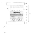
- Fig. 1 represents a thermally assisted switching MRAM element 1 comprising a magnetic tunnel junction 2 according to an embodiment.
- the magnetic tunnel junction 2 comprises a reference layer 21 having a reference magnetization 210, a storage layer 23 having a storage magnetization 320, and a tunnel barrier layer 22 included between the storage layer 23 and the reference layer 21.
- the ferromagnetic reference and storage layers 21, 23 typically comprise a transition metal-based alloy, such a Co, Fe, or Ni-based alloy.
- the tunnel barrier layer 22 is preferably made of a material selected from the group comprising Al 2 O 3 or MgO.
- the tunneling resistance of the magnetic tunnel junction 2 depends exponentially on the thickness of the tunnel barrier layer 22 and is measured by the resistance-area product (RA) of the magnetic tunnel junction 2.
- RA resistance-area product
- the RA must sufficiently small in order to flow a heating current 31 through the magnetic tunnel junction 2 which is sufficiently high to raise the temperature of the antiferromagnetic storage layer 24 at the high threshold temperature.
- the magnetic tunnel junction 2 further comprises an antiferromagnetic storage layer 24 exchange-coupling the storage layer 23 such as to pin the storage magnetization 230 of the storage layer 23 at a low temperature threshold, and to free it at a high temperature threshold.
- the MRAM element 1 can further comprise an electrode / conductive line 5 on each end of the magnetic tunnel junction 2 for passing a current in the magnetic tunnel junction 2.
- Fig. 2 shows the MRAM element 1 in another configuration wherein the storage layer 23 comprises a synthetic storage layer including a first storage ferromagnetic layer 231 having a first storage magnetization 234, a second ferromagnetic layer 233 having a second storage magnetization 235, and a non-magnetic coupling layer 232 separating the first and second ferromagnetic layers 231, 233.
- the dimensions (e.g., thickness) of the spacer layer 232 may be selected to cause the first and second storage layers 231 and 233 to be magnetically coupled via RKKY coupling, such that the first ferromagnetic magnetization 235 is oriented anti-parallel with the second ferromagnetic magnetization 235.
- the thickness may depend on the material that the spacer layer 232 is formed from.
- the spacer layer 232 can comprise a non-magnetic material selected from the group comprising, for example, ruthenium (Ru), rhenium (Re), rhodium (Rh), tellurium (Te), yttrium (Y), chromium (Cr), iridium (Ir), silver (Ag), copper (Cu), etc.
- the thickness may be comprised between about 0.2 nm and 3 nm. However, other thicknesses may be suitable to couple the two storage layers 231 and 233.
- the spacer layer 232 can preferably comprise ruthenium (Ru) and have a thickness being comprised between 0.7 nm and 0.9 nm.
- the antiferromagnetic storage layer 24 is arranged such as to pin the storage magnetization 234 of the first storage layer 231 at the low temperature threshold, and to free it at the high temperature threshold.
- the high threshold temperature corresponding to a writing mode operating temperature
- local ambient temperatures in the vicinity of the MRAM device can be as high as 200°C.
- the antiferromagnetic storage layer 24 has a storage blocking temperature T bs that is comprised between 150°C and 250°C.
- Mn-based metallic alloys are advantageous for antiferromagnetic layers since they combine a large enough exchange field at drive operating temperatures, are highly resistive such as to induce minimum current shunting, they require only low processing temperatures, are corrosion resistant, any they are thermally stable.
- FeMn-based antiferromagnetic layers allow for a relatively low writing mode operating temperature due to its low Néel temperature.
- Reference 1 Nozaires et. al., "Blocking temperature distribution and long-term stability of spin-valve structures with Mn-based antiferromagnets"; J. Appl. Phys. 87, 3920 (2000 ), reports a blocking temperature value of about 170°C for a FeMn layer, 10 nm in thickness.
- Mn-based antiferromagnetic alloys in particular NiMn, PtMn and IrMn-based alloys have a better data retention of the data written in the storage layer 23 than the FeMn-based layer but are also characterized by high writing mode operating temperatures.
- Reference 1 reports a blocking temperature of about 255°C for an IrMn layer 7.5 nm in thickness; of about 310°C for a PtMn layer 35 nm in thickness; and above 400°C for a NiMn layer 25 nm in thickness.
- Antiferromagnetic layers comprising NiMn, PtMn and IrMn thus allow enhancing data retention capability at the cost of a much higher writing mode operating temperature.
- the antiferromagnetic storage layer 24 includes a bilayer structure comprising a first antiferromagnetic layer 241 having a first storage blocking temperature T bs1 , and a second antiferromagnetic layer 242 having a second storage blocking temperature T bs2 .
- the first and second antiferromagnetic layers 241, 242 can be arranged such that the first storage blocking temperature T bs1 is lower than the second storage blocking temperature T bs2 .
- the first and second antiferromagnetic layers 241, 242 can be arranged such that the first storage blocking temperature T bs1 is below 200°C and the second blocking temperature T bs2 is above 250°C.
- the first antiferromagnetic layer 241 comprises a FeMn-based ferromagnetic alloy.
- the FeMn-based alloy is characterised by a relatively low Néel temperature and low first storage blocking temperature T bs1 .
- the first antiferromagnetic layer 241 comprising the FeMn-based ferromagnetic alloy is adjacent with the storage layer 23.
- the second antiferromagnetic layer 242 comprises a Mn-based alloy having a second storage blocking temperature being above 250°C.
- the second antiferromagnetic layer 242 can comprise a Mn-based alloy selected from IrMn, PtMn or NiMn.
- the second layer 242 can comprise a NiMn-based alloy such that the difference between the values of the first and second storage blocking temperature T bs1 , T bs2 is largest.
- the thickness of the first layer 241 and the thickness of the second layer 242 are selected such that the storage blocking temperature T bs of the antiferromagnetic storage layer 24 is comprised between 150°C and 300°C.
- the antiferromagnetic storage layer 24 comprises a multilayer structure including a plurality of the first antiferromagnetic layer 241 and a plurality of the second antiferromagnetic layer 242.
- the two antiferromagnetic layers 241, 242 behave as one antiferromagnetic storage layer 24 having an intermediate value of the storage blocking temperature T bs between the low storage blocking temperature of the FeMn-based first antiferromagnetic layer 241 and the high storage blocking temperature of the other Mn-based second antiferromagnetic layer 242.
- T bs storage blocking temperature
- the composition of the two layers 241, 242 intermix forming an alloy comprising FeMn and IrMn.
- the intermixing occurs in an interfacial region between the two layers 241, 242 that becomes proportionally smaller than the bulk region of the layers 241, 242 were no intermixing occurs. Consequently, increasing the thickness of the layers 241, 242 results in a value of the storage blocking temperature T bs that approaches the first storage blocking temperature T bs1 of the first storage antiferromagnetic layers 241 being made of FeMn. In this latter configuration, a magnetic coupling occurs between the first storage antiferromagnetic layer 241 and the second storage antiferromagnetic layer 242 below the first storage blocking temperature T bs1 .
- the storage blocking temperature T bs of the antiferromagnetic storage layer 24 can thus be tuned by varying the composition and the thickness of each of the first and second antiferromagnetic layers 241, 242.
- each of said plurality of the first antiferromagnetic layer 241 can be magnetically coupled with each of said plurality of the second antiferromagnetic layer 242, and behave as one antiferromagnetic storage layer 24 having an averaged value of the storage blocking temperature T bs . This happens when the operating temperature is below the first storage blocking temperature T bs1 of said each of said plurality of the first antiferromagnetic layer 241, and below the second storage blocking temperature T bs2 of said plurality of the second antiferromagnetic layer 242.
- the storage blocking temperature T bs can further be tuned by varying the composition of each of said plurality of the first and of the second antiferromagnetic layer 241, 242.
- the storage blocking temperature T bs can also be tuned by varying the thickness of each of said plurality of the first and of the second antiferromagnetic layer 241, 242.
- the thickness the first antiferromagnetic layer, 241 is comprised between 0.1 nm and 1 nm, and the thickness of the second antiferromagnetic layer 242 is comprised between 0.1 nm and 5 nm.
- the thickness the first antiferromagnetic layer 241 is comprised between 0.5 nm and 5 nm
- the thickness of the second antiferromagnetic layer 242 is comprised between 0.5 nm and 5 nm.
- the total thickness of the antiferromagnetic storage layer 24 comprising the bilayer structure or the multilayer structure as described herein can be comprised between 5 nm and 50 nm but preferably between 5 nm and 10 nm.
- the temperature dependence of exchange bias field (Hex) is reported in Fig. 4 for the antiferromagnetic storage layer 24 having the multilayer structure (curves 3 to 6).
- the magnetic tunnel junction 2 further comprises a synthetic storage layer 23 wherein the 2 nm thick first storage ferromagnetic layer 231 comprises a CoFeB alloy, the1.5 nm thick second ferromagnetic layer 233 comprises a NiFe alloy, and the 0.2 nm thick non-magnetic coupling layer 232 comprises Ta; a 2 nm thick reference layer 21 comprising a CoFeB alloy; and a tunnel barrier layer 22 made of MgO.
- Fig. 4 also reports the temperature dependence of the exchange bias field (Hex) for the antiferromagnetic storage layer 24 comprising a single layer including a FeMn alloy (curve 2), and an IrMn alloy (curve 1).
- the exchange bias field (Hex) decreases substantially linearly with increasing temperature in all cases (curves 1 to 6).
- the exchange bias field (Hex) decreases faster for the antiferromagnetic storage layer 24 being made of the single FeMn layer (curve 2) than for the multi-layered antiferromagnetic storage layer 24 (curves 3 to 6),
- the antiferromagnetic storage layer 24 comprising the single IrMn layer (curve 1) has the lowest decreases in exchange bias field (Hex) with increasing temperature.
- Curves 5 and 6 represent the case wherein one of the first antiferromagnetic storage layers 241 is in contact with the storage layer 23 (i.e. a sequence of alternating layers of FeMn / IrMn from the storage layer 23).
- Curves 3 and 4 represent the case wherein one of the second antiferromagnetic storage layers 242 is in contact with the storage layer 23 (i.e. a sequence of alternating layers of IrMn / FeMn from the storage layer 23).
- curves 4 and 6 correspond to the antiferromagnetic storage layer 24 comprising ten of each first and second antiferromagnetic storage layers 241, 242, each layer, 241, 242 being 0.5 nm in thickness.
- Curves 3 and 5 correspond to the antiferromagnetic storage layer 24 comprising five of each first and second antiferromagnetic storage layers 241, 242, each layer 241, 242 being 1 nm in thickness.
- higher exchange blas field (Hex) is obtained when one of the antiferromagnetic storage layer 241 in contact with the storage layer 23 comprises the FeMn alloy (curves 5 and 6) than when it comprises the IrMn alloy (curves 3 and 4).
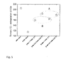
- Fig. 5 reports the storage blocking temperature T bs for the different configurations of the antiferromagnetic storage layer 24 of Fig. 4 .
- the storage blocking temperature T bs is extrapolated at 0°C from the curves 1 to 6.
- the highest storage blocking temperature T bs (about 205°C) is obtained for the antiferromagnetic storage layer 24 having the single IrMn layer while the lowest storage blocking temperature T bs (about 115°C) is obtained for the antiferromagnetic storage layer 24 having the single FeMn layer.
- the antiferromagnetic storage layer 24 comprising the multilayer structure with the 0.5 nm thick layers 241, 242 yields higher storage blocking temperature T bs , i.e., about 180°C and 185°C for the IrMn / FeMn sequence and the FeMn / IrMn sequence, respectively, than for the antiferromagnetic storage layer 24 comprising the multilayer structure with the 1 nm thick layers 241, 242 (data points denoted B in figure 5 ).
- the magnetic tunnel junction 2 further comprises an antiferromagnetic reference layer 25 exchange-coupling the reference layer 21 such as to pin the reference magnetization 210 below a reference blocking temperature T br of the antiferromagnetic reference layer 25.
- the reference magnetization 210 should remain pinned in the whole range of operating temperatures of the MRAM cell in order to avoid losing data written in the reference layer 21.
- the reference magnetization 210 should thus remain pinned at the low and high temperature threshold.
- the difference between the storage blocking temperature T bs of the antiferromagnetic storage layer 23 and the reference blocking temperature T br of the antiferromagnetic storage layer 23 should be larger than at least 50°C in order to achieve a reliable MRAM device.
- a large difference between the storage and reference blocking temperature T bs , T br can be obtained, for example, by the antiferromagnetic reference layer 25 being thick and comprising a NiMn-based alloy having a reference blocking temperature T br that is above 400°C.
- the antiferromagnetic reference layer 25 can also comprise a PtMn or IrMn-based alloy.
- the antiferromagnetic reference layer 25 can further comprise a bilayer structure or a multilayer structure comprising one or a plurality of antiferromagnetic reference layers 25.
- An advantage of the antiferromagnetic storage layer 23 having the bilayer or multilayer structure as disclosed herein is that it combines better data retention, due to the high second storage blocking temperature T bs2 of the second antiferromagnetic layer 242, with low writing mode operating temperatures, due to the low Néel temperature (or low first storage blocking temperature T bs1 ) of the FeMn-based first antiferromagnetic storage layer 241.
Landscapes
- Engineering & Computer Science (AREA)
- Computer Hardware Design (AREA)
- Hall/Mr Elements (AREA)
- Mram Or Spin Memory Techniques (AREA)
- Semiconductor Memories (AREA)
Abstract
Description
- The present invention concerns a thermally assisted switching MRAM element having improved data retention and low writing mode operating temperature.
- Magnetoresistive random access memory (MRAM) devices are solid state, non-volatile memory devices which make use of the tunnel magnetoresistive effect. A conventional MRAM device includes a column of first electrical wires, referred to as word lines, and a row of second electrical wires, referred to as bit lines. An array of magnetic memory cells, located at the junctions of the word lines and bit lines, is used to record data signals. A typical magnetic memory cell comprises a hard magnetic layer, a soft magnetic layer, and a non-magnetic layer sandwiched between the hard magnetic layer and the soft magnetic layer. The hard magnetic layer has a magnetization vector fixed in one direction. The orientation of the magnetization vector does not change under a magnetic field applied thereon. The soft magnetic layer has an alterable magnetization vector under a magnetic field applied thereon, that either points to the same direction, hereinafter "parallel allignrnent", or to the opposite direction, hereinafter "antiparallel alignment", of the magnetization vector of the hard magnetic layer. Since the resistances of the magnetic memory cell in the "parallel alignment" status and the "antiparallel alignment" status are different, the two types of alignment status can be used to record the two logical states, i.e., the "0"s or "1"s of a data bit.
- In a writing operation, an electric current passes through the word line and the bit line adjacent to the memory cell. When the electric current reaches a certain threshold, a magnetic field generated by the electric current will switch the orientation of the magnetization vector of the soft magnetic layer. As a result, the magnetization vector of the hard magnetic layer and the soft magnetic layer will be changed from one type of alignment, e.g. "parallel alignment", to the other type of alignment, e.g. "antiparallel alignment", so that a data signal in form of one data bit can be recorded in the memory cell.
- In MRAM structure design, lower writing power dissipation and a higher cell density are most desired. Unfortunately, a reduction of cell size, i.e. an increase in cell density, will lead to a reduction in the available energy to store the bit data. Further, the error rate increases very rapidly as the cell size scales down. However, in order to reduce the error rate, high anisotropy energy is required to overcome thermal fluctuations. Hard magnetic material has higher anisotropy energy compared with soft magnetic material, but in that case a higher writing current is required. The higher anisotropy energy results in higher writing current density, which unfortunately has the disadvantage of efectro-migration.
- Patent
US5959880 describes an MRAM cell achieving bi-stable switching during the write operation, and good thermal and/or temporal stability of the written data when the ferromagnetic storage layer is made of a material having high magnetocrystalline anisotropy. Writing such a MRAM cell, however, require high field currents able to switch the magnetization direction of the ferromagnetic storage layer from a stable logic state to another, resulting in high power consumption. A decrease in power consumption can be obtained by reducing the magnetocrystalline anisotropy but at the expense of thermal and temporal stability. In other words, the above conventional MRAM cells do not simultaneously fulfil low power consumption and thermal and temporal stability. - In a thermally assisted switching (TAS) -MRAM cell, the storage layer is pinned by an antiferromagnetic layer, such that the magnetization of the storage layer can be oriented only when the MRAM cell is heated at a high temperature threshold, above a critical temperature of the antiferromagnetic layer. An advantage of the TAS-MRAM cell is that a high selectivity to writing can be achieved by the selective heating of the cell to be written. Moreover, the written data can be maintained when the cell is exposed to parasite magnetic fields at ambient temperature. Another advantage is the possibility of reducing significantly the size of the cell without affecting much the writing stability (or data retention). Reduced power consumption during writing can also be achieved.
- Improving further data retention can be achieved by using an antiferromagnetic layer having a higher critical temperature. However, the high critical temperature antiferromagnetic layer requires heating the MRAM cell at higher temperature and, thus resulting in higher power consumption.
- The present disclosure concerns a MRAM element comprising a magnetic tunnel junction including a reference layer having a reference magnetization; a storage layer having a storage magnetization; a tunnel barrier layer included between the storage layer and the reference layer; and a storage antiferromagnetic layer exchange-coupling the storage layer such as to pin the storage magnetization at a low temperature threshold and to free it at a high temperature threshold; the antiferromagnetic layer comprising at least one first layer having a first storage blocking temperature, and at least one second antiferromagnetic layer having a second storage blocking temperature; the first storage blocking temperature being lower than the second storage blocking temperature.
- In an embodiment, the first storage blocking temperature can be below 200°C and the second storage blocking temperature can be above 250°C.
- In another embodiment, said at least one first layer can comprise a FeMn-based alloy. Said at least one second layer can comprise a Mn-based alloy. Said Mn-based alloy can be selected from IrMn, PtMn or NiMn, and preferably a NiMn alloy.
- In yet another embodiment, the antiferromagnetic storage layer can comprise a plurality of the first layer and a plurality of the second layer, each of said plurality of the first antiferromagnetic layer alternating with each of said plurality of the second antiferromagnetic layers.
- In yet another embodiment, the first layer can have a thickness comprised between 0.1 nm and 5 nm and the second layer can have a thickness comprised between 0.1 nm and 5 nm. Preferably, the first layer has a thickness comprised between 0.5 nm and 5 nm and the second layer has a thickness comprised between 0.5 nm and 5 nm. The antiferromagnetic storage layer can have a thickness comprised between 5 nm and 50 nm, but preferably between 5 nm and 10 nm.
- In yet another embodiment, the magnetic tunnel junction can further comprise an antiferromagnetic reference layer exchange-coupling the reference layer such as to pin the reference magnetization below a reference blocking temperature of the antiferromagnetic reference layer.
- The present disclosure also pertains to a MRAM device comprising a plurality of the MRAM element.
- An advantage of the antiferromagnetic storage layer disclosed herein is that it combines the stability of the second antiferromagnetic layer, thus better data retention, with the low Néel temperature of the first antiferromagnetic storage layer, thus low writing mode operating temperature. Another advantage is that the storage blocking temperature of the antiferromagnetic storage layer can be tuned by varying the composition and the thickness of each of the first and second antiferromagnetic layers.
- The invention will be better understood with the aid of the description of an embodiment given by way of example and illustrated by the figures, in which:
-
Fig. 1 represents a MRAM element comprising an antiferromagnetic storage layer according to an embodiment; and -
Fig. 2 shows the MRAM element according to another embodiment; -
Fig. 3 illustrates the antiferromagnetic storage layer 4 comprising a multilayer structure, according to an embodiment; -
Fig. 4 reports the temperature dependence of exchange bias field for the antiferromagnetic storage layer, according to an embodiment; and -
Fig. 5 reports the storage blocking temperature for the antiferromagnetic storage layer ofFig. 4 . -
Fig. 1 represents a thermally assistedswitching MRAM element 1 comprising amagnetic tunnel junction 2 according to an embodiment. Themagnetic tunnel junction 2 comprises areference layer 21 having areference magnetization 210, astorage layer 23 having a storage magnetization 320, and atunnel barrier layer 22 included between thestorage layer 23 and thereference layer 21. The ferromagnetic reference andstorage layers tunnel barrier layer 22 is preferably made of a material selected from the group comprising Al2O3 or MgO. The tunneling resistance of themagnetic tunnel junction 2 depends exponentially on the thickness of thetunnel barrier layer 22 and is measured by the resistance-area product (RA) of themagnetic tunnel junction 2. The RA must sufficiently small in order to flow a heating current 31 through themagnetic tunnel junction 2 which is sufficiently high to raise the temperature of theantiferromagnetic storage layer 24 at the high threshold temperature. Themagnetic tunnel junction 2 further comprises anantiferromagnetic storage layer 24 exchange-coupling thestorage layer 23 such as to pin thestorage magnetization 230 of thestorage layer 23 at a low temperature threshold, and to free it at a high temperature threshold. TheMRAM element 1 can further comprise an electrode /conductive line 5 on each end of themagnetic tunnel junction 2 for passing a current in themagnetic tunnel junction 2. -
Fig. 2 shows theMRAM element 1 in another configuration wherein thestorage layer 23 comprises a synthetic storage layer including a first storageferromagnetic layer 231 having afirst storage magnetization 234, a secondferromagnetic layer 233 having asecond storage magnetization 235, and anon-magnetic coupling layer 232 separating the first and secondferromagnetic layers spacer layer 232 may be selected to cause the first andsecond storage layers ferromagnetic magnetization 235 is oriented anti-parallel with the secondferromagnetic magnetization 235. The thickness may depend on the material that thespacer layer 232 is formed from. For example, thespacer layer 232 can comprise a non-magnetic material selected from the group comprising, for example, ruthenium (Ru), rhenium (Re), rhodium (Rh), tellurium (Te), yttrium (Y), chromium (Cr), iridium (Ir), silver (Ag), copper (Cu), etc. In an embodiment, the thickness may be comprised between about 0.2 nm and 3 nm. However, other thicknesses may be suitable to couple the twostorage layers spacer layer 232 can preferably comprise ruthenium (Ru) and have a thickness being comprised between 0.7 nm and 0.9 nm. In the particular example ofFig. 2 , theantiferromagnetic storage layer 24 is arranged such as to pin thestorage magnetization 234 of thefirst storage layer 231 at the low temperature threshold, and to free it at the high temperature threshold. - Typically, the high threshold temperature, corresponding to a writing mode operating temperature, can range from 150°C up to 250°C. This temperature range is determined in part by the fact that the high threshold temperature should be higher than the highest temperature to which a MRAM device, comprising a plurality of the
MRAM element 1, is submitted during its normal use. For example, in extreme environments such as in spatial, military, automotive applications, local ambient temperatures in the vicinity of the MRAM device can be as high as 200°C. Preferably, theantiferromagnetic storage layer 24 has a storage blocking temperature Tbs that is comprised between 150°C and 250°C. - Mn-based metallic alloys are advantageous for antiferromagnetic layers since they combine a large enough exchange field at drive operating temperatures, are highly resistive such as to induce minimum current shunting, they require only low processing temperatures, are corrosion resistant, any they are thermally stable. FeMn-based antiferromagnetic layers allow for a relatively low writing mode operating temperature due to its low Néel temperature. Reference 1: Nozières et. al., "Blocking temperature distribution and long-term stability of spin-valve structures with Mn-based antiferromagnets"; J. Appl. Phys. 87, 3920 (2000), reports a blocking temperature value of about 170°C for a FeMn layer, 10 nm in thickness.
- On the other hand, other Mn-based antiferromagnetic alloys, in particular NiMn, PtMn and IrMn-based alloys have a better data retention of the data written in the
storage layer 23 than the FeMn-based layer but are also characterized by high writing mode operating temperatures.Reference 1 reports a blocking temperature of about 255°C for an IrMn layer 7.5 nm in thickness; of about 310°C for a PtMn layer 35 nm in thickness; and above 400°C for aNiMn layer 25 nm in thickness. Antiferromagnetic layers comprising NiMn, PtMn and IrMn thus allow enhancing data retention capability at the cost of a much higher writing mode operating temperature. - In the embodiment represented in
Figs. 1 and2 , theantiferromagnetic storage layer 24 includes a bilayer structure comprising a firstantiferromagnetic layer 241 having a first storage blocking temperature Tbs1, and a secondantiferromagnetic layer 242 having a second storage blocking temperature Tbs2. The first and secondantiferromagnetic layers antiferromagnetic layers - In an embodiment, the first
antiferromagnetic layer 241 comprises a FeMn-based ferromagnetic alloy. As discussed above, the FeMn-based alloy is characterised by a relatively low Néel temperature and low first storage blocking temperature Tbs1. Preferably, the firstantiferromagnetic layer 241 comprising the FeMn-based ferromagnetic alloy is adjacent with thestorage layer 23. - In another embodiment, the second
antiferromagnetic layer 242 comprises a Mn-based alloy having a second storage blocking temperature being above 250°C. In particular, the secondantiferromagnetic layer 242 can comprise a Mn-based alloy selected from IrMn, PtMn or NiMn. preferably, thesecond layer 242 can comprise a NiMn-based alloy such that the difference between the values of the first and second storage blocking temperature Tbs1, Tbs2 is largest. - In yet another embodiment, the thickness of the
first layer 241 and the thickness of thesecond layer 242 are selected such that the storage blocking temperature Tbs of theantiferromagnetic storage layer 24 is comprised between 150°C and 300°C. - In yet another embodiment, the
antiferromagnetic storage layer 24 comprises a multilayer structure including a plurality of the firstantiferromagnetic layer 241 and a plurality of the secondantiferromagnetic layer 242. An example of theantiferromagnetic storage layer 24 comprising such multilayer structure represented inFig. 3 wherein each of said plurality of the firstantiferromagnetic layer 241 alternates with each of said plurality of the secondantiferromagnetic layers 242. - In the case the first and second
antiferromagnetic layer antiferromagnetic storage layer 24 are thin, i.e., having a thickness of 1 nm and below, the twoantiferromagnetic layers antiferromagnetic storage layer 24 having an intermediate value of the storage blocking temperature Tbs between the low storage blocking temperature of the FeMn-based firstantiferromagnetic layer 241 and the high storage blocking temperature of the other Mn-based secondantiferromagnetic layer 242. Indeed, during post-deposition annealing of thelayers layers antiferromagnetic layers layers layers layers antiferromagnetic layers 241 being made of FeMn. In this latter configuration, a magnetic coupling occurs between the first storageantiferromagnetic layer 241 and the second storageantiferromagnetic layer 242 below the first storage blocking temperature Tbs1. At and above the first storage blocking temperature Tbs1, the magnetic coupling between the first storageantiferromagnetic layer 241 and the second storageantiferromagnetic layer 242 disappears and the storageantiferromagnetic layers 24 is no more exchange-coupled with thestorage layer 23. The storage blocking temperature Tbs of theantiferromagnetic storage layer 24 can thus be tuned by varying the composition and the thickness of each of the first and secondantiferromagnetic layers - Similarly to the bilayer structure of the
antiferromagnetic storage layer 24 as shown in the examples ofFigs. 1 and2 , each of said plurality of the firstantiferromagnetic layer 241 can be magnetically coupled with each of said plurality of the secondantiferromagnetic layer 242, and behave as oneantiferromagnetic storage layer 24 having an averaged value of the storage blocking temperature Tbs. This happens when the operating temperature is below the first storage blocking temperature Tbs1 of said each of said plurality of the firstantiferromagnetic layer 241, and below the second storage blocking temperature Tbs2 of said plurality of the secondantiferromagnetic layer 242. - Similarly to the bilayer structure, the storage blocking temperature Tbs can further be tuned by varying the composition of each of said plurality of the first and of the second
antiferromagnetic layer antiferromagnetic layer - In an embodiment, the thickness the first antiferromagnetic layer, 241 is comprised between 0.1 nm and 1 nm, and the thickness of the second
antiferromagnetic layer 242 is comprised between 0.1 nm and 5 nm. Preferably the thickness the firstantiferromagnetic layer 241 is comprised between 0.5 nm and 5 nm, and the thickness of the secondantiferromagnetic layer 242 is comprised between 0.5 nm and 5 nm. The total thickness of theantiferromagnetic storage layer 24 comprising the bilayer structure or the multilayer structure as described herein can be comprised between 5 nm and 50 nm but preferably between 5 nm and 10 nm. - The temperature dependence of exchange bias field (Hex) is reported in
Fig. 4 for theantiferromagnetic storage layer 24 having the multilayer structure (curves 3 to 6). Here, themagnetic tunnel junction 2 further comprises asynthetic storage layer 23 wherein the 2 nm thick first storageferromagnetic layer 231 comprises a CoFeB alloy, the1.5 nm thick secondferromagnetic layer 233 comprises a NiFe alloy, and the 0.2 nm thicknon-magnetic coupling layer 232 comprises Ta; a 2 nmthick reference layer 21 comprising a CoFeB alloy; and atunnel barrier layer 22 made of MgO.Fig. 4 . also reports the temperature dependence of the exchange bias field (Hex) for theantiferromagnetic storage layer 24 comprising a single layer including a FeMn alloy (curve 2), and an IrMn alloy (curve 1). - The exchange bias field (Hex) decreases substantially linearly with increasing temperature in all cases (
curves 1 to 6). The exchange bias field (Hex) decreases faster for theantiferromagnetic storage layer 24 being made of the single FeMn layer (curve 2) than for the multi-layered antiferromagnetic storage layer 24 (curves 3 to 6), Theantiferromagnetic storage layer 24 comprising the single IrMn layer (curve 1) has the lowest decreases in exchange bias field (Hex) with increasing temperature. -
Curves 5 and 6 represent the case wherein one of the first antiferromagnetic storage layers 241 is in contact with the storage layer 23 (i.e. a sequence of alternating layers of FeMn / IrMn from the storage layer 23). Curves 3 and 4 represent the case wherein one of the second antiferromagnetic storage layers 242 is in contact with the storage layer 23 (i.e. a sequence of alternating layers of IrMn / FeMn from the storage layer 23). Moreover, curves 4 and 6 correspond to theantiferromagnetic storage layer 24 comprising ten of each first and second antiferromagnetic storage layers 241, 242, each layer, 241, 242 being 0.5 nm in thickness.Curves 3 and 5 correspond to theantiferromagnetic storage layer 24 comprising five of each first and second antiferromagnetic storage layers 241, 242, eachlayer Fig. 4 , higher exchange blas field (Hex) is obtained when one of theantiferromagnetic storage layer 241 in contact with thestorage layer 23 comprises the FeMn alloy (curves 5 and 6) than when it comprises the IrMn alloy (curves 3 and 4). Higher exchange bias field (Hex) is also obtained for theantiferromagnetic storage layer 24 comprising 0.5 nm thick antiferromagnetic storage layers 241, 242 (curves 4 and 6) than for theantiferromagnetic storage layer 24 comprising 1 nm thick antiferromagnetic storage layers 241, 242 (curves 3 and 5). -
Fig. 5 reports the storage blocking temperature Tbs for the different configurations of theantiferromagnetic storage layer 24 ofFig. 4 . The storage blocking temperature Tbs is extrapolated at 0°C from thecurves 1 to 6. The highest storage blocking temperature Tbs (about 205°C) is obtained for theantiferromagnetic storage layer 24 having the single IrMn layer while the lowest storage blocking temperature Tbs (about 115°C) is obtained for theantiferromagnetic storage layer 24 having the single FeMn layer. Theantiferromagnetic storage layer 24 comprising the multilayer structure with the 0.5 nmthick layers 241, 242 (data points denoted A infigure 5 ) yields higher storage blocking temperature Tbs, i.e., about 180°C and 185°C for the IrMn / FeMn sequence and the FeMn / IrMn sequence, respectively, than for theantiferromagnetic storage layer 24 comprising the multilayer structure with the 1 nmthick layers 241, 242 (data points denoted B infigure 5 ). - In yet another embodiment, the
magnetic tunnel junction 2 further comprises anantiferromagnetic reference layer 25 exchange-coupling thereference layer 21 such as to pin thereference magnetization 210 below a reference blocking temperature Tbr of theantiferromagnetic reference layer 25. Here, thereference magnetization 210 should remain pinned in the whole range of operating temperatures of the MRAM cell in order to avoid losing data written in thereference layer 21. In particular, thereference magnetization 210 should thus remain pinned at the low and high temperature threshold. Moreover, the difference between the storage blocking temperature Tbs of theantiferromagnetic storage layer 23 and the reference blocking temperature Tbr of theantiferromagnetic storage layer 23 should be larger than at least 50°C in order to achieve a reliable MRAM device. A large difference between the storage and reference blocking temperature Tbs, Tbr can be obtained, for example, by theantiferromagnetic reference layer 25 being thick and comprising a NiMn-based alloy having a reference blocking temperature Tbr that is above 400°C. Alternatively, theantiferromagnetic reference layer 25 can also comprise a PtMn or IrMn-based alloy. Theantiferromagnetic reference layer 25 can further comprise a bilayer structure or a multilayer structure comprising one or a plurality of antiferromagnetic reference layers 25. - An advantage of the
antiferromagnetic storage layer 23 having the bilayer or multilayer structure as disclosed herein is that it combines better data retention, due to the high second storage blocking temperature Tbs2 of the secondantiferromagnetic layer 242, with low writing mode operating temperatures, due to the low Néel temperature (or low first storage blocking temperature Tbs1) of the FeMn-based firstantiferromagnetic storage layer 241. -
- 1
- magnetic random access memory (MRAM) cell
- 2
- magnetic tunnel junction
- 21
- reference layer
- 210
- reference magnetization
- 22
- tunnel barrier layer
- 23
- storage layer
- 230
- storage magnetization
- 231
- first storage ferromagnetic layer
- 232
- spacer layer
- 233
- second storage ferromagnetic layer
- 234
- first storage magnetization
- 235
- second storage magnetization
- 24
- antiferromagnetic storage layer
- 241
- first antiferromagnetic layer
- 242
- second antiferromagnetic layer
- 5
- electrode / conductive line
- Tbs
- storage blocking temperature
- Tbs1
- first storage blocking temperature
- Tbs2
- second storage blocking temperature
- Tbr
- reference blocking temperature
Claims (12)
- A MRAM element (1) comprising a magnetic tunnel junction (2) including a reference layer (21) having a reference magnetization (210); a storage layer (23) having a storage magnetization (230, 234, 235); a tunnel barrier layer (22) included between the storage layer (23) and the reference layer (21); and a storage antiferromagnetic layer (24) exchange-coupling the storage layer (23) such as to pin the storage magnetization (230, 234, 235) at a low temperature threshold and to free it at a high temperature threshold;
the antiferromagnetic layer (24) comprising at least one first layer (241) having a first storage blocking temperature (Tbs1), and at least one second antiferromagnetic layer (242) having a second storage blocking temperature (Tbs2); the first storage blocking temperature (Tbs1) being lower than the second storage blocking temperature (Tbs2). - MRAM element (1) according to claim 1, wherein the first storage blocking temperature (Tbs1) is below 200°C and the second storage blocking temperature (Tbs2) is above 250°C
- MRAM element (1) according to the claims 1 or 2, wherein said at least one first layer (241) comprises a FeMn-based alloy.
- MRAM element (1) according to any one of claims 1 to 3, wherein
said at least one second layer (242) comprises a Mn-based alloy. - MRAM element (1) according to claim 4, wherein
said Mn-based alloy is selected from IrMn, PtMn or NiMn. - MRAM element (1) according to claim 4, wherein
said Mn-based alloy is a NiMn alloy. - MRAM element (1) according to any of the claims 1 to 6,
wherein
the antiferromagnetic storage layer (24) comprises a plurality of the first layer (241) and a plurality of the second layer (242), wherein each of said plurality of the first antiferromagnetic layer (241) alternates with each of said plurality of the second antiferromagnetic layers (242). - MRAM element (1) according to any of the claims 1 to 7,
wherein
the first layer (241) has a thickness comprised between 0.1 nm and 5 nm and the second layer (242) has a thickness comprised between 0.1 nm and 5 nm. - MRAM element (1) according to any of the claims 1 to 7,
wherein
the first layer (241) has a thickness comprised between 0.5 nm and 5 nm and the second layer (242) has a thickness comprised between 0.5 nm and 5 nm. - MRAM element (1) according to any of the claim 1 to 9,
wherein
the antiferromagnetic storage layer (24) has a thickness comprised between 5 nm and 50 nm, but preferably between 5 nm and 10 nm. - MRAM element (1) according to any of the claims 1 to 9,
wherein
the magnetic tunnel junction (2) further comprises an antiferromagnetic reference layer (25) exchange-coupling the reference layer (21) such as to pin the reference magnetization (210) below a reference blocking temperature (Tbr) of the antiferromagnetic reference layer (25). - MRAM device, comprising a plurality of the MRAM element (1) characterized by any one of the claims 1 to 11.
Priority Applications (3)
| Application Number | Priority Date | Filing Date | Title |
|---|---|---|---|
| EP12290196.0A EP2672488B1 (en) | 2012-06-08 | 2012-06-08 | MRAM element having improved data retention and low writing temperature |
| US14/405,918 US9331268B2 (en) | 2012-06-08 | 2013-06-07 | MRAM element having improved data retention and low writing temperature |
| PCT/EP2013/061851 WO2013182701A1 (en) | 2012-06-08 | 2013-06-07 | Mram element having improved data retention and low writing temperature |
Applications Claiming Priority (1)
| Application Number | Priority Date | Filing Date | Title |
|---|---|---|---|
| EP12290196.0A EP2672488B1 (en) | 2012-06-08 | 2012-06-08 | MRAM element having improved data retention and low writing temperature |
Publications (2)
| Publication Number | Publication Date |
|---|---|
| EP2672488A1 true EP2672488A1 (en) | 2013-12-11 |
| EP2672488B1 EP2672488B1 (en) | 2015-08-19 |
Family
ID=46758701
Family Applications (1)
| Application Number | Title | Priority Date | Filing Date |
|---|---|---|---|
| EP12290196.0A Not-in-force EP2672488B1 (en) | 2012-06-08 | 2012-06-08 | MRAM element having improved data retention and low writing temperature |
Country Status (3)
| Country | Link |
|---|---|
| US (1) | US9331268B2 (en) |
| EP (1) | EP2672488B1 (en) |
| WO (1) | WO2013182701A1 (en) |
Families Citing this family (5)
| Publication number | Priority date | Publication date | Assignee | Title |
|---|---|---|---|---|
| US9384811B2 (en) | 2014-04-10 | 2016-07-05 | Samsung Electronics Co., Ltd. | Method and system for providing a thermally assisted spin transfer torque magnetic device including smart thermal barriers |
| US9324939B2 (en) | 2014-07-01 | 2016-04-26 | Qualcomm Incorporated | Synthetic antiferromagnet (SAF) coupled free layer for perpendicular magnetic tunnel junction (p-MTJ) |
| US9685604B2 (en) * | 2015-08-31 | 2017-06-20 | Taiwan Semiconductor Manufacturing Company, Ltd. | Magnetoresistive random access memory cell and fabricating the same |
| KR20170064018A (en) * | 2015-11-30 | 2017-06-09 | 에스케이하이닉스 주식회사 | Electronic device |
| US11630002B2 (en) * | 2021-02-08 | 2023-04-18 | Macronix International Co., Ltd. | Method for sensing temperature in memory die, memory die and memory with temperature sensing function |
Citations (3)
| Publication number | Priority date | Publication date | Assignee | Title |
|---|---|---|---|---|
| US5959880A (en) | 1997-12-18 | 1999-09-28 | Motorola, Inc. | Low aspect ratio magnetoresistive tunneling junction |
| US20100072524A1 (en) * | 2005-09-20 | 2010-03-25 | Yiming Huai | Magnetic Devices Having Oxide Antiferromagnetic Layer Next To Free Ferromagnetic Layer |
| US20110110151A1 (en) * | 2009-05-08 | 2011-05-12 | Crocus Technology Sa | Magnetic memory with a thermally assisted spin transfer torque writing procedure using a low writing current |
-
2012
- 2012-06-08 EP EP12290196.0A patent/EP2672488B1/en not_active Not-in-force
-
2013
- 2013-06-07 US US14/405,918 patent/US9331268B2/en active Active
- 2013-06-07 WO PCT/EP2013/061851 patent/WO2013182701A1/en not_active Ceased
Patent Citations (3)
| Publication number | Priority date | Publication date | Assignee | Title |
|---|---|---|---|---|
| US5959880A (en) | 1997-12-18 | 1999-09-28 | Motorola, Inc. | Low aspect ratio magnetoresistive tunneling junction |
| US20100072524A1 (en) * | 2005-09-20 | 2010-03-25 | Yiming Huai | Magnetic Devices Having Oxide Antiferromagnetic Layer Next To Free Ferromagnetic Layer |
| US20110110151A1 (en) * | 2009-05-08 | 2011-05-12 | Crocus Technology Sa | Magnetic memory with a thermally assisted spin transfer torque writing procedure using a low writing current |
Non-Patent Citations (1)
| Title |
|---|
| NOZIÈRCS: "Blocking temperature distribution and long-term stability of spin-valve structures with Mn-based antiferromagnets", J. APPL. PHYS., vol. 87, 2000, pages 3920 |
Also Published As
| Publication number | Publication date |
|---|---|
| US9331268B2 (en) | 2016-05-03 |
| WO2013182701A1 (en) | 2013-12-12 |
| US20150123224A1 (en) | 2015-05-07 |
| EP2672488B1 (en) | 2015-08-19 |
Similar Documents
| Publication | Publication Date | Title |
|---|---|---|
| US6593608B1 (en) | Magneto resistive storage device having double tunnel junction | |
| CN102473450B (en) | Magnetic stack having reference layers with orthogonal magnetization orientation directions | |
| US7359235B2 (en) | Separate write and read access architecture for a magnetic tunnel junction | |
| US8362534B2 (en) | Flux-closed STRAM with electronically reflective insulative spacer | |
| US8288023B2 (en) | Magnetic memory cell construction | |
| EP2385529B1 (en) | STRAM with electronically reflective insulative spacers | |
| US6576969B2 (en) | Magneto-resistive device having soft reference layer | |
| EP2575135B1 (en) | Magnetic random access memory (MRAM) cell and method for reading the MRAM cell using a self-referenced read operation | |
| US7983075B2 (en) | Nonvolatile memory device | |
| EP2447949B1 (en) | Multi level magnetic element | |
| US20170092851A1 (en) | Magnetic memory device and method of fabricating the same | |
| US8743597B2 (en) | Self-referenced magnetic random access memory element comprising a synthetic storage layer | |
| US20180061887A1 (en) | Magnetoresistive random access memory (mram) with an interconnect that generates a spin current and a magnetic field effect | |
| US20130108889A1 (en) | Magnetoresistance Device and Memory Device Including the Magnetoresistance Device | |
| EP2249349B1 (en) | Magnetic memory with a thermally assisted writing procedure and reduced writng field | |
| US9331268B2 (en) | MRAM element having improved data retention and low writing temperature | |
| US20100103565A1 (en) | St-ram employing heusler alloys | |
| US5828598A (en) | MRAM with high GMR ratio | |
| US20100091564A1 (en) | Magnetic stack having reduced switching current | |
| US9679624B2 (en) | Magnetic random access memory (MRAM) cell with low power consumption | |
| KR20240009333A (en) | Spin-orbit torque magnetic random-access memory(SOT-MRAM) device |
Legal Events
| Date | Code | Title | Description |
|---|---|---|---|
| PUAI | Public reference made under article 153(3) epc to a published international application that has entered the european phase |
Free format text: ORIGINAL CODE: 0009012 |
|
| AK | Designated contracting states |
Kind code of ref document: A1 Designated state(s): AL AT BE BG CH CY CZ DE DK EE ES FI FR GB GR HR HU IE IS IT LI LT LU LV MC MK MT NL NO PL PT RO RS SE SI SK SM TR |
|
| AX | Request for extension of the european patent |
Extension state: BA ME |
|
| 17P | Request for examination filed |
Effective date: 20140512 |
|
| RBV | Designated contracting states (corrected) |
Designated state(s): AL AT BE BG CH CY CZ DE DK EE ES FI FR GB GR HR HU IE IS IT LI LT LU LV MC MK MT NL NO PL PT RO RS SE SI SK SM TR |
|
| GRAP | Despatch of communication of intention to grant a patent |
Free format text: ORIGINAL CODE: EPIDOSNIGR1 |
|
| INTG | Intention to grant announced |
Effective date: 20150409 |
|
| GRAS | Grant fee paid |
Free format text: ORIGINAL CODE: EPIDOSNIGR3 |
|
| GRAA | (expected) grant |
Free format text: ORIGINAL CODE: 0009210 |
|
| AK | Designated contracting states |
Kind code of ref document: B1 Designated state(s): AL AT BE BG CH CY CZ DE DK EE ES FI FR GB GR HR HU IE IS IT LI LT LU LV MC MK MT NL NO PL PT RO RS SE SI SK SM TR |
|
| REG | Reference to a national code |
Ref country code: GB Ref legal event code: FG4D |
|
| REG | Reference to a national code |
Ref country code: CH Ref legal event code: EP |
|
| REG | Reference to a national code |
Ref country code: IE Ref legal event code: FG4D |
|
| REG | Reference to a national code |
Ref country code: AT Ref legal event code: REF Ref document number: 744298 Country of ref document: AT Kind code of ref document: T Effective date: 20150915 |
|
| REG | Reference to a national code |
Ref country code: DE Ref legal event code: R096 Ref document number: 602012009734 Country of ref document: DE |
|
| REG | Reference to a national code |
Ref country code: FR Ref legal event code: GC Effective date: 20151118 |
|
| REG | Reference to a national code |
Ref country code: AT Ref legal event code: MK05 Ref document number: 744298 Country of ref document: AT Kind code of ref document: T Effective date: 20150819 |
|
| REG | Reference to a national code |
Ref country code: LT Ref legal event code: MG4D |
|
| REG | Reference to a national code |
Ref country code: NL Ref legal event code: MP Effective date: 20150819 |
|
| PG25 | Lapsed in a contracting state [announced via postgrant information from national office to epo] |
Ref country code: GR Free format text: LAPSE BECAUSE OF FAILURE TO SUBMIT A TRANSLATION OF THE DESCRIPTION OR TO PAY THE FEE WITHIN THE PRESCRIBED TIME-LIMIT Effective date: 20151120 Ref country code: NO Free format text: LAPSE BECAUSE OF FAILURE TO SUBMIT A TRANSLATION OF THE DESCRIPTION OR TO PAY THE FEE WITHIN THE PRESCRIBED TIME-LIMIT Effective date: 20151119 Ref country code: LV Free format text: LAPSE BECAUSE OF FAILURE TO SUBMIT A TRANSLATION OF THE DESCRIPTION OR TO PAY THE FEE WITHIN THE PRESCRIBED TIME-LIMIT Effective date: 20150819 Ref country code: LT Free format text: LAPSE BECAUSE OF FAILURE TO SUBMIT A TRANSLATION OF THE DESCRIPTION OR TO PAY THE FEE WITHIN THE PRESCRIBED TIME-LIMIT Effective date: 20150819 Ref country code: FI Free format text: LAPSE BECAUSE OF FAILURE TO SUBMIT A TRANSLATION OF THE DESCRIPTION OR TO PAY THE FEE WITHIN THE PRESCRIBED TIME-LIMIT Effective date: 20150819 |
|
| PG25 | Lapsed in a contracting state [announced via postgrant information from national office to epo] |
Ref country code: SE Free format text: LAPSE BECAUSE OF FAILURE TO SUBMIT A TRANSLATION OF THE DESCRIPTION OR TO PAY THE FEE WITHIN THE PRESCRIBED TIME-LIMIT Effective date: 20150819 Ref country code: AT Free format text: LAPSE BECAUSE OF FAILURE TO SUBMIT A TRANSLATION OF THE DESCRIPTION OR TO PAY THE FEE WITHIN THE PRESCRIBED TIME-LIMIT Effective date: 20150819 Ref country code: RS Free format text: LAPSE BECAUSE OF FAILURE TO SUBMIT A TRANSLATION OF THE DESCRIPTION OR TO PAY THE FEE WITHIN THE PRESCRIBED TIME-LIMIT Effective date: 20150819 Ref country code: IS Free format text: LAPSE BECAUSE OF FAILURE TO SUBMIT A TRANSLATION OF THE DESCRIPTION OR TO PAY THE FEE WITHIN THE PRESCRIBED TIME-LIMIT Effective date: 20151219 Ref country code: PL Free format text: LAPSE BECAUSE OF FAILURE TO SUBMIT A TRANSLATION OF THE DESCRIPTION OR TO PAY THE FEE WITHIN THE PRESCRIBED TIME-LIMIT Effective date: 20150819 Ref country code: ES Free format text: LAPSE BECAUSE OF FAILURE TO SUBMIT A TRANSLATION OF THE DESCRIPTION OR TO PAY THE FEE WITHIN THE PRESCRIBED TIME-LIMIT Effective date: 20150819 Ref country code: PT Free format text: LAPSE BECAUSE OF FAILURE TO SUBMIT A TRANSLATION OF THE DESCRIPTION OR TO PAY THE FEE WITHIN THE PRESCRIBED TIME-LIMIT Effective date: 20151221 |
|
| PG25 | Lapsed in a contracting state [announced via postgrant information from national office to epo] |
Ref country code: NL Free format text: LAPSE BECAUSE OF FAILURE TO SUBMIT A TRANSLATION OF THE DESCRIPTION OR TO PAY THE FEE WITHIN THE PRESCRIBED TIME-LIMIT Effective date: 20150819 |
|
| PG25 | Lapsed in a contracting state [announced via postgrant information from national office to epo] |
Ref country code: CZ Free format text: LAPSE BECAUSE OF FAILURE TO SUBMIT A TRANSLATION OF THE DESCRIPTION OR TO PAY THE FEE WITHIN THE PRESCRIBED TIME-LIMIT Effective date: 20150819 Ref country code: IT Free format text: LAPSE BECAUSE OF FAILURE TO SUBMIT A TRANSLATION OF THE DESCRIPTION OR TO PAY THE FEE WITHIN THE PRESCRIBED TIME-LIMIT Effective date: 20150819 Ref country code: DK Free format text: LAPSE BECAUSE OF FAILURE TO SUBMIT A TRANSLATION OF THE DESCRIPTION OR TO PAY THE FEE WITHIN THE PRESCRIBED TIME-LIMIT Effective date: 20150819 Ref country code: EE Free format text: LAPSE BECAUSE OF FAILURE TO SUBMIT A TRANSLATION OF THE DESCRIPTION OR TO PAY THE FEE WITHIN THE PRESCRIBED TIME-LIMIT Effective date: 20150819 Ref country code: SK Free format text: LAPSE BECAUSE OF FAILURE TO SUBMIT A TRANSLATION OF THE DESCRIPTION OR TO PAY THE FEE WITHIN THE PRESCRIBED TIME-LIMIT Effective date: 20150819 |
|
| REG | Reference to a national code |
Ref country code: DE Ref legal event code: R097 Ref document number: 602012009734 Country of ref document: DE |
|
| PG25 | Lapsed in a contracting state [announced via postgrant information from national office to epo] |
Ref country code: RO Free format text: LAPSE BECAUSE OF FAILURE TO SUBMIT A TRANSLATION OF THE DESCRIPTION OR TO PAY THE FEE WITHIN THE PRESCRIBED TIME-LIMIT Effective date: 20150819 |
|
| PLBE | No opposition filed within time limit |
Free format text: ORIGINAL CODE: 0009261 |
|
| STAA | Information on the status of an ep patent application or granted ep patent |
Free format text: STATUS: NO OPPOSITION FILED WITHIN TIME LIMIT |
|
| REG | Reference to a national code |
Ref country code: FR Ref legal event code: PLFP Year of fee payment: 5 |
|
| 26N | No opposition filed |
Effective date: 20160520 |
|
| PG25 | Lapsed in a contracting state [announced via postgrant information from national office to epo] |
Ref country code: SI Free format text: LAPSE BECAUSE OF FAILURE TO SUBMIT A TRANSLATION OF THE DESCRIPTION OR TO PAY THE FEE WITHIN THE PRESCRIBED TIME-LIMIT Effective date: 20150819 |
|
| PG25 | Lapsed in a contracting state [announced via postgrant information from national office to epo] |
Ref country code: BE Free format text: LAPSE BECAUSE OF FAILURE TO SUBMIT A TRANSLATION OF THE DESCRIPTION OR TO PAY THE FEE WITHIN THE PRESCRIBED TIME-LIMIT Effective date: 20150819 |
|
| PG25 | Lapsed in a contracting state [announced via postgrant information from national office to epo] |
Ref country code: MC Free format text: LAPSE BECAUSE OF FAILURE TO SUBMIT A TRANSLATION OF THE DESCRIPTION OR TO PAY THE FEE WITHIN THE PRESCRIBED TIME-LIMIT Effective date: 20150819 |
|
| REG | Reference to a national code |
Ref country code: CH Ref legal event code: PL |
|
| REG | Reference to a national code |
Ref country code: IE Ref legal event code: MM4A |
|
| PG25 | Lapsed in a contracting state [announced via postgrant information from national office to epo] |
Ref country code: CH Free format text: LAPSE BECAUSE OF NON-PAYMENT OF DUE FEES Effective date: 20160630 Ref country code: LI Free format text: LAPSE BECAUSE OF NON-PAYMENT OF DUE FEES Effective date: 20160630 |
|
| PG25 | Lapsed in a contracting state [announced via postgrant information from national office to epo] |
Ref country code: IE Free format text: LAPSE BECAUSE OF NON-PAYMENT OF DUE FEES Effective date: 20160608 |
|
| REG | Reference to a national code |
Ref country code: FR Ref legal event code: PLFP Year of fee payment: 6 |
|
| PG25 | Lapsed in a contracting state [announced via postgrant information from national office to epo] |
Ref country code: HU Free format text: LAPSE BECAUSE OF FAILURE TO SUBMIT A TRANSLATION OF THE DESCRIPTION OR TO PAY THE FEE WITHIN THE PRESCRIBED TIME-LIMIT; INVALID AB INITIO Effective date: 20120608 Ref country code: SM Free format text: LAPSE BECAUSE OF FAILURE TO SUBMIT A TRANSLATION OF THE DESCRIPTION OR TO PAY THE FEE WITHIN THE PRESCRIBED TIME-LIMIT Effective date: 20150819 Ref country code: CY Free format text: LAPSE BECAUSE OF FAILURE TO SUBMIT A TRANSLATION OF THE DESCRIPTION OR TO PAY THE FEE WITHIN THE PRESCRIBED TIME-LIMIT Effective date: 20150819 |
|
| REG | Reference to a national code |
Ref country code: FR Ref legal event code: PLFP Year of fee payment: 7 |
|
| PG25 | Lapsed in a contracting state [announced via postgrant information from national office to epo] |
Ref country code: TR Free format text: LAPSE BECAUSE OF FAILURE TO SUBMIT A TRANSLATION OF THE DESCRIPTION OR TO PAY THE FEE WITHIN THE PRESCRIBED TIME-LIMIT Effective date: 20150819 Ref country code: MK Free format text: LAPSE BECAUSE OF FAILURE TO SUBMIT A TRANSLATION OF THE DESCRIPTION OR TO PAY THE FEE WITHIN THE PRESCRIBED TIME-LIMIT Effective date: 20150819 Ref country code: LU Free format text: LAPSE BECAUSE OF NON-PAYMENT OF DUE FEES Effective date: 20160608 Ref country code: MT Free format text: LAPSE BECAUSE OF NON-PAYMENT OF DUE FEES Effective date: 20160630 Ref country code: HR Free format text: LAPSE BECAUSE OF FAILURE TO SUBMIT A TRANSLATION OF THE DESCRIPTION OR TO PAY THE FEE WITHIN THE PRESCRIBED TIME-LIMIT Effective date: 20150819 |
|
| PG25 | Lapsed in a contracting state [announced via postgrant information from national office to epo] |
Ref country code: BG Free format text: LAPSE BECAUSE OF FAILURE TO SUBMIT A TRANSLATION OF THE DESCRIPTION OR TO PAY THE FEE WITHIN THE PRESCRIBED TIME-LIMIT Effective date: 20150819 |
|
| PG25 | Lapsed in a contracting state [announced via postgrant information from national office to epo] |
Ref country code: AL Free format text: LAPSE BECAUSE OF FAILURE TO SUBMIT A TRANSLATION OF THE DESCRIPTION OR TO PAY THE FEE WITHIN THE PRESCRIBED TIME-LIMIT Effective date: 20150819 |
|
| REG | Reference to a national code |
Ref country code: DE Ref legal event code: R082 Ref document number: 602012009734 Country of ref document: DE Representative=s name: BECK & ROESSIG EUROPEAN PATENT ATTORNEYS, DE Ref country code: DE Ref legal event code: R082 Ref document number: 602012009734 Country of ref document: DE Representative=s name: BECK & ROESSIG - EUROPEAN PATENT ATTORNEYS, DE |
|
| P01 | Opt-out of the competence of the unified patent court (upc) registered |
Effective date: 20230620 |
|
| REG | Reference to a national code |
Ref country code: DE Ref legal event code: R081 Ref document number: 602012009734 Country of ref document: DE Owner name: CROCUS TECHNOLOGY SA, FR Free format text: FORMER OWNER: CROCUS TECHNOLOGY S.A., GRENOBLE, FR Ref country code: DE Ref legal event code: R081 Ref document number: 602012009734 Country of ref document: DE Owner name: ALLEGRO MICRO SYSTEMS LLC, MANCHESTER, US Free format text: FORMER OWNER: CROCUS TECHNOLOGY S.A., GRENOBLE, FR Ref country code: DE Ref legal event code: R081 Ref document number: 602012009734 Country of ref document: DE Owner name: ALLEGRO MICRO SYSTEMS LLC, WILMINGTON, US Free format text: FORMER OWNER: CROCUS TECHNOLOGY S.A., GRENOBLE, FR |
|
| REG | Reference to a national code |
Ref country code: DE Ref legal event code: R081 Ref document number: 602012009734 Country of ref document: DE Owner name: ALLEGRO MICRO SYSTEMS LLC, MANCHESTER, US Free format text: FORMER OWNER: CROCUS TECHNOLOGY SA, GRENOBLE, FR Ref country code: DE Ref legal event code: R081 Ref document number: 602012009734 Country of ref document: DE Owner name: ALLEGRO MICRO SYSTEMS LLC, WILMINGTON, US Free format text: FORMER OWNER: CROCUS TECHNOLOGY SA, GRENOBLE, FR |
|
| REG | Reference to a national code |
Ref country code: DE Ref legal event code: R081 Ref document number: 602012009734 Country of ref document: DE Owner name: ALLEGRO MICRO SYSTEMS LLC, MANCHESTER, US Free format text: FORMER OWNER: ALLEGRO MICRO SYSTEMS LLC, WILMINGTON, DE, US |
|
| REG | Reference to a national code |
Ref country code: GB Ref legal event code: 732E Free format text: REGISTERED BETWEEN 20240229 AND 20240306 |
|
| PGFP | Annual fee paid to national office [announced via postgrant information from national office to epo] |
Ref country code: GB Payment date: 20240509 Year of fee payment: 13 |
|
| PGFP | Annual fee paid to national office [announced via postgrant information from national office to epo] |
Ref country code: DE Payment date: 20240507 Year of fee payment: 13 |
|
| PGFP | Annual fee paid to national office [announced via postgrant information from national office to epo] |
Ref country code: FR Payment date: 20240509 Year of fee payment: 13 |
|
| REG | Reference to a national code |
Ref country code: DE Ref legal event code: R119 Ref document number: 602012009734 Country of ref document: DE |
|
| GBPC | Gb: european patent ceased through non-payment of renewal fee |
Effective date: 20250608 |
|
| PG25 | Lapsed in a contracting state [announced via postgrant information from national office to epo] |
Ref country code: GB Free format text: LAPSE BECAUSE OF NON-PAYMENT OF DUE FEES Effective date: 20250608 |
|
| PG25 | Lapsed in a contracting state [announced via postgrant information from national office to epo] |
Ref country code: DE Free format text: LAPSE BECAUSE OF NON-PAYMENT OF DUE FEES Effective date: 20260101 |
|
| PG25 | Lapsed in a contracting state [announced via postgrant information from national office to epo] |
Ref country code: FR Free format text: LAPSE BECAUSE OF NON-PAYMENT OF DUE FEES Effective date: 20250630 |