EP2667612A2 - Display device and control method thereof - Google Patents
Display device and control method thereof Download PDFInfo
- Publication number
- EP2667612A2 EP2667612A2 EP20130169060 EP13169060A EP2667612A2 EP 2667612 A2 EP2667612 A2 EP 2667612A2 EP 20130169060 EP20130169060 EP 20130169060 EP 13169060 A EP13169060 A EP 13169060A EP 2667612 A2 EP2667612 A2 EP 2667612A2
- Authority
- EP
- European Patent Office
- Prior art keywords
- image
- generate
- read
- resolution
- processing
- Prior art date
- Legal status (The legal status is an assumption and is not a legal conclusion. Google has not performed a legal analysis and makes no representation as to the accuracy of the status listed.)
- Granted
Links
Images




Classifications
-
- G—PHYSICS
- G09—EDUCATION; CRYPTOGRAPHY; DISPLAY; ADVERTISING; SEALS
- G09G—ARRANGEMENTS OR CIRCUITS FOR CONTROL OF INDICATING DEVICES USING STATIC MEANS TO PRESENT VARIABLE INFORMATION
- G09G5/00—Control arrangements or circuits for visual indicators common to cathode-ray tube indicators and other visual indicators
- G09G5/36—Control arrangements or circuits for visual indicators common to cathode-ray tube indicators and other visual indicators characterised by the display of a graphic pattern, e.g. using an all-points-addressable [APA] memory
- G09G5/39—Control of the bit-mapped memory
- G09G5/393—Arrangements for updating the contents of the bit-mapped memory
-
- H—ELECTRICITY
- H04—ELECTRIC COMMUNICATION TECHNIQUE
- H04N—PICTORIAL COMMUNICATION, e.g. TELEVISION
- H04N19/00—Methods or arrangements for coding, decoding, compressing or decompressing digital video signals
- H04N19/10—Methods or arrangements for coding, decoding, compressing or decompressing digital video signals using adaptive coding
- H04N19/102—Methods or arrangements for coding, decoding, compressing or decompressing digital video signals using adaptive coding characterised by the element, parameter or selection affected or controlled by the adaptive coding
- H04N19/103—Selection of coding mode or of prediction mode
- H04N19/112—Selection of coding mode or of prediction mode according to a given display mode, e.g. for interlaced or progressive display mode
-
- H—ELECTRICITY
- H04—ELECTRIC COMMUNICATION TECHNIQUE
- H04N—PICTORIAL COMMUNICATION, e.g. TELEVISION
- H04N19/00—Methods or arrangements for coding, decoding, compressing or decompressing digital video signals
- H04N19/10—Methods or arrangements for coding, decoding, compressing or decompressing digital video signals using adaptive coding
- H04N19/134—Methods or arrangements for coding, decoding, compressing or decompressing digital video signals using adaptive coding characterised by the element, parameter or criterion affecting or controlling the adaptive coding
- H04N19/157—Assigned coding mode, i.e. the coding mode being predefined or preselected to be further used for selection of another element or parameter
- H04N19/16—Assigned coding mode, i.e. the coding mode being predefined or preselected to be further used for selection of another element or parameter for a given display mode, e.g. for interlaced or progressive display mode
-
- G—PHYSICS
- G09—EDUCATION; CRYPTOGRAPHY; DISPLAY; ADVERTISING; SEALS
- G09G—ARRANGEMENTS OR CIRCUITS FOR CONTROL OF INDICATING DEVICES USING STATIC MEANS TO PRESENT VARIABLE INFORMATION
- G09G2340/00—Aspects of display data processing
- G09G2340/02—Handling of images in compressed format, e.g. JPEG, MPEG
-
- G—PHYSICS
- G09—EDUCATION; CRYPTOGRAPHY; DISPLAY; ADVERTISING; SEALS
- G09G—ARRANGEMENTS OR CIRCUITS FOR CONTROL OF INDICATING DEVICES USING STATIC MEANS TO PRESENT VARIABLE INFORMATION
- G09G2360/00—Aspects of the architecture of display systems
- G09G2360/18—Use of a frame buffer in a display terminal, inclusive of the display panel
Definitions
- the processing unit 204 processes the outputs of the transformation units 202 and 203 to generate the output image S DATA1 and S DATA2 .
- the display panel 101 sequentially displays two images according to the output images S DATA1 and S DATA2 .
- the invention does not limit how the processing unit 204 processes the outputs of the transformation units 202 and 203.
- the processing unit 204 processes the outputs of the transformation units 202 and 203 according to an over-driving (OD) process.
- OD over-driving
- the storage module 205 stores another input image S I2 and provides the read-out image S R2 according to the stored input image S I2 .
- the read-out image S R2 is the same as the input image S I2 . Since the input image S I2 is a second image, the storage module 205 serves the previous image (i.e. the input image S I1 ) as the processing image S P1 .
Landscapes
- Engineering & Computer Science (AREA)
- Multimedia (AREA)
- Signal Processing (AREA)
- Physics & Mathematics (AREA)
- Computer Hardware Design (AREA)
- General Physics & Mathematics (AREA)
- Theoretical Computer Science (AREA)
- Control Of Indicators Other Than Cathode Ray Tubes (AREA)
- Transforming Electric Information Into Light Information (AREA)
- Controls And Circuits For Display Device (AREA)
Abstract
Description
- This Application claims priority of Taiwan Patent Application No.
101118467, filed on May 24, 2012 101118661, filed on May 25, 2012 - The disclosure relates to a display device, and more particularly to a display device, which is capable of reducing a bandwidth of a memory.
- Because cathode ray tubes (CRTs) are inexpensive and provide high definition, they are utilized extensively in televisions and computers. With technological development, new flat-panel displays are continually being developed. When a larger display panel is required, the weight of the flat-panel display does not substantially change when compared to CRT displays.
- With an increase in the resolution of the display panel, an amount of image data required by the display panel is increased. To access the image data, a conventional method increases the number and bandwidth of memory. Thus, the cost of the flat-panel display is increased.
- In accordance with an embodiment, a display device comprises a display panel and a timing controller. The display panel displays an image according to an output image. The timing controller comprises a receiving unit, a first transformation unit, a second transformation unit and a processing unit. The receiving unit generates a processing image and a read-out image according to a first input image and a second input image. The first transformation unit transforms the processing image to generate a first transformed image. The second transformation unit transforms the read-out image to generate a second transformed image. The processing unit processes the first and the second transformed images to generate the output image. A resolution of the processing image and a resolution of the read-out image are less than a resolution of the display panel.
- In accordance with a further embodiment, a method comprises: receiving a first input image and a second input image; storing the first and the second input images and generating a processing image and a read-out image; transforming the processing image to generate a first transformed image; transforming the read-out image to generate a second transformed image; processing the first and the second transformed images to generate an output image; and providing the output image to a display device to display an image. A resolution of the processing image and a resolution of the read-out image are less than a resolution of the display device.
- A detailed description is given in the following embodiments with reference to the accompanying drawings.
- The invention can be more fully understood by referring to the following detailed description and examples with references made to the accompanying drawings, wherein:
-
FIG. 1 is a schematic diagram of an exemplary embodiment of a display device; -
FIGs. 2-5 are schematic diagrams of other exemplary embodiments of the timing controller; and -
FIGs. 6-7 are schematic diagrams of other exemplary embodiments of a control method. - The following description is exemplary embodiments of carrying out the invention. This description is made for the purpose of illustrating the general principles of the invention and should not be taken in a limiting sense. The scope of the invention is best determined by reference to the appended claims.
-
FIG. 1 is a schematic diagram of an exemplary embodiment of a display device. Thedisplay device 100 comprises adisplay panel 101 and a timing controller (TCON) 102. In this embodiment, thetiming controller 102 controls thedisplay panel 101 via a flexible printed circuit (FPC) 103 such that an image is displayed by thedisplay panel 101. The invention does not limit the kind of thedisplay panel 101. In one embodiment, thedisplay panel 101 is a self-luminescent panel or a reflective panel. In another embodiment, the resolution of thedisplay panel 101 is 3840x2160. - The invention does not limit the kind of the
display device 100. In one embodiment, thedisplay device 100 is a personal digital assistant (PDA), a cellular phone, a digital camera (DSC), a television, a global positioning system (GPS), a car display, an avionics display, a digital photo frame, a notebook computer (NB), or a personal computer (PC). - In this embodiment, the
display panel 101 comprisesscan groups data group 130 and adisplay region 160, but the disclosure is not limited thereto. In other embodiments, any circuit structure can be applied in thedisplay panel 101, as long as the circuit structure is capable of displaying an image in thedisplay region 160. - As shown in
FIG. 1 , thescan group 110 is placed on the left hand side of thedisplay region 160 and comprisesgate drivers 111∼114. Thescan group 120 is placed on the right hand side of thedisplay region 160 and comprises gate drivers 115∼118. Thegate drivers 111∼118 provide a plurality of scan signals to pixels in thedisplay region 160. The invention does not limit the number and the position of the scan groups. In one embodiment, thedisplay panel 101 only comprises a single scan group and is placed on any side of thedisplay region 160. In another embodiment, the number of the gate drivers is proportional to the number of the pixels in thedisplay region 160. - In this embodiment, the
data group 130 comprisessource drivers 131∼154 to provide a plurality of data signals to the pixels in thedisplay region 160. The invention does not limit the number of the source drivers. In one embodiment, the number of the source drivers is proportional to the number of the pixels in thedisplay region 160. - The
timing controller 102 generates a serial output image SDATA to thedisplay panel 101 according to a serial input image SI such that thedisplay panel 101 displays a serial image according to the serial output image SDATA. The invention does not limit the format of the input image SI. In one embodiment, the input image SI is a low voltage differential signaling (LVDS) format. -
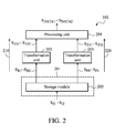
FIG. 2 is a schematic diagram of an exemplary embodiment of the timing controller. Thetiming controller 102 sequentially receives input images SI1 and SI2 and sequentially generates output images SDATA1∼SDATA2. In this embodiment, thetiming controller 102 comprises areceiving unit 201,transformation units processing unit 204. - The
receiving unit 201 generates read-out images SR1∼SR2 according to the input images SI1∼SI2. In this embodiment, thereceiving unit 201 comprises astorage module 205 to store the input images SI1∼SI2 and serves the input images SI1∼SI2 as the read-out images SR1∼SR2. In one embodiment, the resolutions of the read-out images SR1∼SR2 are equal to the resolutions of the input images SI1∼SI2, such as 1920x1080. - In this embodiment, the
receiving unit 201 further provides processing images SP0∼SP1. The invention does not limit the relationship between the processing images SP0∼SP1 and the read-out images SR1∼SR2. In one embodiment, the resolutions of the processing images SP0∼SP1 are equal to the resolutions of the read-out images SR1∼SR2. In another embodiment, the processing image SP0 is a pre-determined image, and the processing image SP1 is the same as the read-out image SR1. In other embodiments, the resolutions of the processing images SP0∼SP1 and read-out images SR1∼SR2 are less than the resolution of thedisplay panel 101. The resolution of thedisplay panel 101 may be 3840x2160. - The
transformation unit 202 transforms the read-out images SR1∼SR2 to generate transformed images ST21∼ST22. In this embodiment, after transformation, the resolutions of the transformed images ST21∼ST22 are larger than the resolutions of the read-out images SR1 ∼SR2. In one embodiment, the resolution of one of the transformed images ST21∼ST22 is equal to the resolution of thedisplay panel 101. - The
transformation unit 203 transforms the processing images SP0∼SP1 to generate transformed images ST31∼ST32. Similarly, after transformation, the resolutions of the transformed images ST31∼ST32 are larger than the resolutions of the processing images SP0∼SP1. In this embodiment, the resolution of one of the transformed images ST31∼ST32 is equal to the resolution of thedisplay panel 101. - The invention does not limit the circuit structures of the
transformation units transformation unit 202 as an example, any circuit structure can serve as thetransformation unit 202, as long as the circuit structure is capable of adjusting the resolutions of the read-out images SR1 and SR2. In one embodiment, thetransformation unit 202 is a Scaler or a super resolution processor. - The
processing unit 204 processes the outputs of thetransformation units display panel 101 sequentially displays two images according to the output images SDATA1 and SDATA2. The invention does not limit how theprocessing unit 204 processes the outputs of thetransformation units processing unit 204 processes the outputs of thetransformation units - In this embodiment, the
transformation unit 202 provides afirst path 210 to transmit present image information and thetransformation unit 203 provides asecond path 220 to transmit previous image information for an OD process. Theprocessing unit 204 executes the OD process for the image information transmitted by thepaths - During a first period, the
storage module 205 stores the input signal SI1 and provides the read-out image SR1 according to the stored input signal SI1. In this embodiment, the input signal SI1 is the same as the read-out image SR1. Since the input signal SI1 is a first image, thestorage module 205 provides a pre-determined image (e.g. SP0) to thetransformation unit 203. In this embodiment, the processing image SP0 is served as a previous image information. - The
transformation units processing unit 204 processes a present image (i.e. the transformed image ST21) and a previous image (i.e. the transformed image ST31) to generate the output image SDATA1 according to an OD process. - During a second period, the
storage module 205 stores another input image SI2 and provides the read-out image SR2 according to the stored input image SI2. In this embodiment, the read-out image SR2 is the same as the input image SI2. Since the input image SI2 is a second image, thestorage module 205 serves the previous image (i.e. the input image SI1) as the processing image SP1. - The
transformation units processing unit 204 processes the transformed images ST22 and ST32 to generate the output image SDATA2 according to an OD process. - In this embodiment, since the resolution of each image stored in the
storage module 205 is less than the resolution of thedisplay panel 101, the bandwidth of thestorage module 205 is reduced. Taking a display panel as an example, assume the resolution of the display panel is 4k2k (i.e. 3840x2160). When the resolutions of the input images SI1 and SI2 are 3840x2160, the bandwidth and amount of thestorage module 205 are required to be increased to store large image information. However, in this embodiment, the resolutions of the input images SI1 and SI2 are less than the resolution of the display panel. Thus, the bandwidth and amount of thestorage module 205 are not required to be increased. In other embodiments, with an increase in the resolution of the display panel, the resolution of the display panel may be higher than 4k2k. In this case, the bandwidth and amount of thestorage module 205 are not increased. -
FIG. 3 is a schematic diagram of another exemplary embodiment of the timing controller.FIG. 3 is similar toFIG. 2 with the exception that the receivingunit 301 comprises astorage module 305, acompression module 306 and adecompression module 307. Since the operations of thetransformation units processing unit 304 are the same as the operations of thetransformation units processing unit 204, the descriptions of thetransformation units processing unit 304 are omitted for brevity. - In this embodiment, when the
transformation unit 302 transforms the read-out image SR1 or SR2, thecompression module 306 compresses the read-out image SR1 or SR2 to generate a compressed image SRC1 or SRC2. Thedecompression module 307 decompresses the compressed image SRC0 or SRC1 stored in thestorage module 305 and serves the decompressed result (e.g. the decompressed image SRCD0 or SRCD1) as the processing image SP0 or SP1. - The compressed image SRC1 or SRC2 generated by the
compression module 306 is stored in thestorage module 305 to replace the un-compressed image (e.g. SI1 or SI2). Thus, the bandwidth of thestorage module 305 can be reduced. -
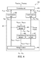
FIG. 4 is a schematic diagram of another exemplary embodiment of the timing controller.FIG. 4 is similar toFIG. 3 except for the addition of an adjustment module 408. Since the operations of the transformation units 402, 403 and theprocessing unit 404 are the same as the operations of thetransformation units processing unit 304, the descriptions of the transformation units 402, 403 and theprocessing unit 404 are omitted for brevity. - In this embodiment, when the transformation unit 402 processes the read-out image SR1 or SR2, the adjustment module 408 adjusts the read-out image SR1 or SR2 to generate an adjusted image SA1 or SA2 according to the reference condition SREF1 or SREF2. The
compression module 406 compresses the adjusted image SA1 or SA2 and stores the compressed result (e.g. SAC1 or SAC2) in thestorage module 405. - The invention does not limit the source of the reference condition SREF1 or SREF2. In one embodiment, the reference conditions SREF1 and SREF2 are pre-determined. In another embodiment, the reference conditions SREF1 and SREF2 are previous images, such as the processing image SP0 and SP1.
- The invention does not limit how the adjustment module 408 adjusts the read-out images SR1∼SR2. In one embodiment, the adjustment module 408 executes an OD process. Taking the read-out images SR2 as an example, the adjustment module 408 utilizes the OD process to process the reference condition SREF2 and the read-out images SR2 to generate an adjusted image SA2, wherein the reference condition SREF2 is the processing image SP1.
-
FIG. 5 is a schematic diagram of another exemplary embodiment of the timing controller.FIG. 5 is similar toFIG. 4 except for the additions of acompression module 509 and adecompression module 510. Since the operations of thetransformation units processing unit 504 are the same as the operations of the transformation units 402, 403 and theprocessing unit 404, the descriptions of thetransformation units processing unit 504 are omitted for brevity. - The
compression module 509 compresses the input images SI1 and SI2 to generate compressed images SC1 and SC2. The compressed images SC1 and SC2 are stored in thestorage module 505. Thedecompression module 510 decompresses the compressed images SC1 and SC2 stored in thestorage module 505 to generate decompressed images SCD1 and SCD2. In this embodiment, the decompressed images SCD1 and SCD2 are served as the read-out images SR1 and SR2. -
FIG. 6 is a schematic diagram of an exemplary embodiment of a control method. The control method is applied in a display device to display an image. First, a first input image and a second input image are received (step S601). The invention does not limit the formats of the first and the second input images. In one embodiment, the formats of the first and the second input images are LVDS formats. In another embodiment, the resolutions of the first and the second input images are 1920x1080. - The first and the second input images are stored and a processing image and a read-out image are generated (step S602). In one embodiment, the first and the second input images are stored in a DRAM. Additionally, the invention does not limit the generations of the processing image and the read-out image. In one embodiment, the processing image and the read-out image relate to the first and the second input images.
- For example, during a first period, the first input image is stored and served as a read-out image. At this time, no a previous image occurred before the first input image such that a pre-determined image is beforehand stored and served as a processing image.
- During a second period, the second input image is stored and served as another read-out image. At this time, since the first input image is a previous image occurring before the second input image, the first input image is served as a processing image. In this embodiment, the processing image is previous information and the read-out image is the present information.
-
FIG. 7 is a schematic diagram of an exemplary embodiment of step S602. In step S701, an input image is compressed to generate a compressed image. The compressed image is stored (step S702). In step S703, the stored compressed image is decompressed. The decompressed result is served as a read-out image or a processing image. - For example, after receiving the first and the second input images, the first and the second input images are compressed to generate a first compressed image and a second compressed image. The first and the second compressed images are stored in a memory. Since the memory directly stores the compressed images, the usable space of the memory is increased and the bandwidth of the memory is reduced. When the memory is accessed, the stored compressed image is decompressed and the decompressed image is served as a processing image or a read-out image.
- Refer to
FIG. 6 , step S603 is to transform the processing image to generate a first transformed image. In this embodiment, after transformation of the processing image, the resolution of the first transformed image is larger than the resolution of the processing image. In one embodiment, the resolution of the first transformed image is four times the resolution of the processing image. - The read-out image is transformed to generate a second transformed image (step S604). In this embodiment, the resolution of the second transformed image is larger than the resolution of the read-out image. In one embodiment, the resolutions of the first and the second transformed images are the same. Additionally, the resolution of the read-out image is the same as the resolution of the processing image.
- The first and the second transformed images are processed to generate an output image (step S605) and the output image is provided to the display device to display an image (step S606). The invention does not limit how the first and the second transformed images are processed. In one embodiment, step S605 is to execute an OD process, but the disclosure is not limited thereto. In other embodiments, the first and the second transformed images are processed to generate information to be displayed in the display device according to other image processes.
- In this embodiment, the resolutions of the processing image and the read-out image generated by step S602 are less than the resolution of the display device. For example, the resolutions of the processing image and the read-out image may be 1920x1080 and the resolution of the display device may be 3840x2160. In another embodiment, the resolution of the first transformed image generated by step S603 and the resolution of the second transformed image generated by step S604 are equal to the resolution of the display device.
- In one embodiment, step S602 is to store the first and the second input images in a DRAM. Thus, data stored in the DRAM is directly served as a processing image or a read-out image. In another embodiment, step S602 is to compress the first and the second input images and then store the compressed images into the DRAM. In this case, data stored in the DRAM is first decompressed and then the decompressed result is served as the processing image or the read-out image.
- In other embodiments, since the read-out image transformed by step S604 is present image information, when the read-out image is transformed, a transformed image segment of the read-out image is compressed and the compressed result replaces a portion of the read-out image stored in the DRAM. The stored compressed result can be served as previous image information. Since the DRAM is not required to store a transformed image, the bandwidth of the DRAM can be reduced, wherein the transformed image is not be compressed.
- Before compressing, a reference condition is utilized to adjust an image data segment of a transformed image and the adjusted result is compressed. In one embodiment, the image data segment of the transformed image and the reference condition are processed by an OD process. In another embodiment, the reference condition is previous image information.
- Since the data stored in the memory is replaced by the compressed image, the bandwidth of the memory can be reduced. Additionally, if the memory stores an un-compressed image, since the resolution of the un-compressed image is less than the resolution of the display device, the memory still has a large usable space.
- Unless otherwise defined, all terms (including technical and scientific terms) used herein have the same meaning as commonly understood by one of ordinary skill in the art to which this invention belongs. It will be further understood that terms, such as those defined in commonly used dictionaries, should be interpreted as having a meaning that is consistent with their meaning in the context of the relevant art and will not be interpreted in an idealized or overly formal sense unless expressly so defined herein.
- While the invention has been described by way of example and in terms of the preferred embodiments, it is to be understood that the invention is not limited to the disclosed embodiments. To the contrary, it is intended to cover various modifications and similar arrangements (as would be apparent to those skilled in the art). Therefore, the scope of the appended claims should be accorded the broadest interpretation so as to encompass all such modifications and similar arrangements.
Claims (20)
- A display device (100), comprising:a display panel (101) displaying an image according to an output image; anda timing controller (102) comprising:a receiving unit (201; 301) generating a processing image and a read-out image according to a first input image and a second input image;a first transformation unit (202; 302) transforming the processing image to generate a first transformed image;a second transformation unit (203; 303) transforming the read-out image to generate a second transformed image; anda processing unit (204; 304) processing the first and the second transformed images to generate the output image, wherein a resolution of the processing image and a resolution of the read-out image are less than a resolution of the display panel.
- The display device (100) as claimed in claim 1, wherein a resolution of the first transformed image is larger than the resolution of the processing image.
- The display device (100) as claimed in claim 1 or 2, wherein a resolution of the second transformed image is larger than the resolution of the read-out image.
- The display device (100) as claimed in one of the preceding claims, wherein a resolution of the first transformed image is equal to the resolution of the display panel.
- The display device (100) as claimed in one of the preceding claims, wherein the processing unit processes the first and the second transformed images according to an over-driving process.
- The display device (100) as claimed in one of the preceding claims, wherein the receiving unit (301) comprises:a compression module (306) compressing the read-out image to generate a compressed image;a storage module (305) storing the compressed image; anda decompression module (307) decompressing the compressed image stored in the storage module to generate the processing image.
- The display device as claimed in one of the preceding claims, wherein the receiving unit (301) comprises:an adjustment module (408; 508) adjusting the read-out image to generate an adjusted image according to a reference condition;a first compression module (406; 506) compressing the adjusted image to generate a first compressed image;a storage module (405) storing the first compressed image; anda first decompression module (407; 507) decompressing the first compressed image stored in the storage module to generate the processing image.
- The display device as claimed in claim 7, wherein the receiving unit further comprises
a second compression module (509) compressing the first input image to generate a second compressed image, wherein the second compressed image is stored in the storage module; and
a second decompression module (510) decompressing the second compressed image stored in the storage module to generate the read-out image. - The display device as claimed in claim 7, wherein the reference condition is the processing image.
- The display device as claimed in claim 9, wherein the adjustment module (408; 508) adjusts the reference condition and the read-out image according to an over-driving process to generate the adjusted image.
- A control method, comprising:receiving a first input image and a second input image (S601);storing the first and the second input images and generating a processing image and a read-out image (S602);transforming the processing image to generate a first transformed image (S603);transforming the read-out image to generate a second transformed image (S604);processing the first and the second transformed images to generate an output image (S605); andproviding the output image to a display device to display an image (S606), wherein a resolution of the processing image and a resolution of the read-out image are less than a resolution of the display device.
- The control method as claimed in claim 11, wherein a resolution of the first transformed image is larger than the resolution of the processing image.
- The control method as claimed in claim 12, wherein the resolution of the first transformed image is four times the resolution of the processing image.
- The control method as claimed in claim 12 or 13, wherein the resolution of the first transformed image is equal to the resolution of the display device.
- The control method as claimed in one of claims 11 - 14, wherein the step of processing the first and the second transformed images to generate the output image is to execute an over-driving process for the first and the second transformed images.
- The control method as claimed in one of claims 11 - 15, further comprising:compressing the read-out image to generate a compressed image (S701);storing the compressed image to generate a stored compressed image (S702); anddecompressing the stored compressed image to generate the processing image (S703);.
- The control method as claimed in one of claims 11-16, further comprising:adjusting the read-out image to generate an adjusted image according to a reference condition;compressing the adjusted image to generate a first compressed image;storing the first compressed image to generate a first stored compressed image; anddecompressing the first stored compressed image to generate the processing image.
- The control method as claimed in claim 17, further comprising:compressing the first input image to generate a second compressed image;storing the second compressed image to generate a second stored compressed image; anddecompressing the second stored compressed image to generate the read-out image.
- The control method as claimed in claim 17 or 18, wherein the reference condition is the processing image.
- The control method as claimed in claim 19, wherein the step of adjusting the read-out image to generate the adjusted image according to the reference condition is to execute an over-driving process for the reference condition and the read-out image.
Applications Claiming Priority (2)
| Application Number | Priority Date | Filing Date | Title |
|---|---|---|---|
| TW101118467A TWI490851B (en) | 2012-05-24 | 2012-05-24 | Display device and control method thereof |
| TW101118661A TWI533282B (en) | 2012-05-25 | 2012-05-25 | Display device and control method thereof |
Publications (3)
| Publication Number | Publication Date |
|---|---|
| EP2667612A2 true EP2667612A2 (en) | 2013-11-27 |
| EP2667612A3 EP2667612A3 (en) | 2014-10-22 |
| EP2667612B1 EP2667612B1 (en) | 2016-02-24 |
Family
ID=48607013
Family Applications (2)
| Application Number | Title | Priority Date | Filing Date |
|---|---|---|---|
| EP13169059.6A Withdrawn EP2667611A3 (en) | 2012-05-24 | 2013-05-24 | Display device and control method thereof |
| EP13169060.4A Active EP2667612B1 (en) | 2012-05-24 | 2013-05-24 | Display device and control method thereof |
Family Applications Before (1)
| Application Number | Title | Priority Date | Filing Date |
|---|---|---|---|
| EP13169059.6A Withdrawn EP2667611A3 (en) | 2012-05-24 | 2013-05-24 | Display device and control method thereof |
Country Status (1)
| Country | Link |
|---|---|
| EP (2) | EP2667611A3 (en) |
Family Cites Families (5)
| Publication number | Priority date | Publication date | Assignee | Title |
|---|---|---|---|---|
| US7773099B2 (en) * | 2007-06-28 | 2010-08-10 | Mitsubishi Electric Research Laboratories, Inc. | Context aware image conversion method and playback system |
| TWI391895B (en) * | 2007-07-16 | 2013-04-01 | Novatek Microelectronics Corp | Display driving apparatus and method thereof |
| TW200921612A (en) * | 2007-11-08 | 2009-05-16 | Etron Technology Inc | An overdrive device for enhancing the response time of LCD display |
| KR100973561B1 (en) * | 2008-06-25 | 2010-08-03 | 삼성전자주식회사 | Display |
| JP5358482B2 (en) * | 2010-02-24 | 2013-12-04 | 株式会社ルネサスエスピードライバ | Display drive circuit |
-
2013
- 2013-05-24 EP EP13169059.6A patent/EP2667611A3/en not_active Withdrawn
- 2013-05-24 EP EP13169060.4A patent/EP2667612B1/en active Active
Non-Patent Citations (1)
| Title |
|---|
| None |
Also Published As
| Publication number | Publication date |
|---|---|
| EP2667611A3 (en) | 2014-10-08 |
| EP2667611A2 (en) | 2013-11-27 |
| EP2667612B1 (en) | 2016-02-24 |
| EP2667612A3 (en) | 2014-10-22 |
Similar Documents
| Publication | Publication Date | Title |
|---|---|---|
| CN110322821B (en) | Source driver and display driver including the same | |
| US20090160883A1 (en) | Information processing apparatus | |
| US10186226B2 (en) | Transparent display device and method of compensating an image for the same | |
| EP3116228B1 (en) | Method and device for adaptively compressing image data | |
| US10559241B2 (en) | Display device and method for displaying image using the same | |
| US9898986B2 (en) | Display device capable of performing black frame insertion | |
| US11837190B2 (en) | Display apparatus and control method thereof | |
| JP6389279B2 (en) | Display interface bandwidth modulation | |
| US7495647B2 (en) | LCD blur reduction through frame rate control | |
| US20130314422A1 (en) | Display device and control method thereof | |
| EP2669886A1 (en) | Image processing method and image display system utilizing the same | |
| CN103426386B (en) | Display device and control method thereof | |
| EP2667612B1 (en) | Display device and control method thereof | |
| US8345055B2 (en) | Image display device | |
| US9530383B2 (en) | Display apparatus and driving method thereof | |
| US8970568B2 (en) | Display device and control method thereof | |
| US8494253B2 (en) | Three-dimensional (3D) image processing method and system | |
| US9355604B2 (en) | Overdriving control method with image compression control and related circuit | |
| CN109102770B (en) | Low-power-consumption low-bandwidth display panel driving chip for high-performance calculation | |
| CN101114429B (en) | Flat panel display and image driving method thereof | |
| CN111028753B (en) | Data-driven delay compensation device and method thereof, and display device | |
| US20240221585A1 (en) | Display device and electronic equipment | |
| KR101578208B1 (en) | Liquid crystal display device and driving method thereof | |
| CN103426387A (en) | Display device and control method thereof | |
| US20120002104A1 (en) | Portable display apparatus of video signal |
Legal Events
| Date | Code | Title | Description |
|---|---|---|---|
| PUAI | Public reference made under article 153(3) epc to a published international application that has entered the european phase |
Free format text: ORIGINAL CODE: 0009012 |
|
| AK | Designated contracting states |
Kind code of ref document: A2 Designated state(s): AL AT BE BG CH CY CZ DE DK EE ES FI FR GB GR HR HU IE IS IT LI LT LU LV MC MK MT NL NO PL PT RO RS SE SI SK SM TR |
|
| AX | Request for extension of the european patent |
Extension state: BA ME |
|
| PUAL | Search report despatched |
Free format text: ORIGINAL CODE: 0009013 |
|
| AK | Designated contracting states |
Kind code of ref document: A3 Designated state(s): AL AT BE BG CH CY CZ DE DK EE ES FI FR GB GR HR HU IE IS IT LI LT LU LV MC MK MT NL NO PL PT RO RS SE SI SK SM TR |
|
| AX | Request for extension of the european patent |
Extension state: BA ME |
|
| RIC1 | Information provided on ipc code assigned before grant |
Ipc: H04N 19/112 20140101ALI20140925BHEP Ipc: H04N 19/16 20140101ALI20140925BHEP Ipc: G09G 5/393 20060101AFI20140925BHEP |
|
| 17P | Request for examination filed |
Effective date: 20150417 |
|
| RBV | Designated contracting states (corrected) |
Designated state(s): AL AT BE BG CH CY CZ DE DK EE ES FI FR GB GR HR HU IE IS IT LI LT LU LV MC MK MT NL NO PL PT RO RS SE SI SK SM TR |
|
| REG | Reference to a national code |
Ref country code: DE Ref legal event code: R079 Ref document number: 602013005115 Country of ref document: DE Free format text: PREVIOUS MAIN CLASS: H04N0007260000 Ipc: G09G0005393000 |
|
| RIC1 | Information provided on ipc code assigned before grant |
Ipc: H04N 19/16 20140101ALI20150619BHEP Ipc: H04N 19/112 20140101ALI20150619BHEP Ipc: G09G 5/393 20060101AFI20150619BHEP |
|
| GRAP | Despatch of communication of intention to grant a patent |
Free format text: ORIGINAL CODE: EPIDOSNIGR1 |
|
| INTG | Intention to grant announced |
Effective date: 20150813 |
|
| GRAS | Grant fee paid |
Free format text: ORIGINAL CODE: EPIDOSNIGR3 |
|
| GRAA | (expected) grant |
Free format text: ORIGINAL CODE: 0009210 |
|
| AK | Designated contracting states |
Kind code of ref document: B1 Designated state(s): AL AT BE BG CH CY CZ DE DK EE ES FI FR GB GR HR HU IE IS IT LI LT LU LV MC MK MT NL NO PL PT RO RS SE SI SK SM TR |
|
| REG | Reference to a national code |
Ref country code: GB Ref legal event code: FG4D |
|
| REG | Reference to a national code |
Ref country code: CH Ref legal event code: EP |
|
| REG | Reference to a national code |
Ref country code: AT Ref legal event code: REF Ref document number: 777091 Country of ref document: AT Kind code of ref document: T Effective date: 20160315 |
|
| REG | Reference to a national code |
Ref country code: IE Ref legal event code: FG4D |
|
| REG | Reference to a national code |
Ref country code: DE Ref legal event code: R096 Ref document number: 602013005115 Country of ref document: DE |
|
| REG | Reference to a national code |
Ref country code: FR Ref legal event code: PLFP Year of fee payment: 4 |
|
| REG | Reference to a national code |
Ref country code: LT Ref legal event code: MG4D |
|
| REG | Reference to a national code |
Ref country code: NL Ref legal event code: MP Effective date: 20160224 |
|
| REG | Reference to a national code |
Ref country code: AT Ref legal event code: MK05 Ref document number: 777091 Country of ref document: AT Kind code of ref document: T Effective date: 20160224 |
|
| PG25 | Lapsed in a contracting state [announced via postgrant information from national office to epo] |
Ref country code: ES Free format text: LAPSE BECAUSE OF FAILURE TO SUBMIT A TRANSLATION OF THE DESCRIPTION OR TO PAY THE FEE WITHIN THE PRESCRIBED TIME-LIMIT Effective date: 20160224 Ref country code: GR Free format text: LAPSE BECAUSE OF FAILURE TO SUBMIT A TRANSLATION OF THE DESCRIPTION OR TO PAY THE FEE WITHIN THE PRESCRIBED TIME-LIMIT Effective date: 20160525 Ref country code: HR Free format text: LAPSE BECAUSE OF FAILURE TO SUBMIT A TRANSLATION OF THE DESCRIPTION OR TO PAY THE FEE WITHIN THE PRESCRIBED TIME-LIMIT Effective date: 20160224 Ref country code: FI Free format text: LAPSE BECAUSE OF FAILURE TO SUBMIT A TRANSLATION OF THE DESCRIPTION OR TO PAY THE FEE WITHIN THE PRESCRIBED TIME-LIMIT Effective date: 20160224 Ref country code: IT Free format text: LAPSE BECAUSE OF FAILURE TO SUBMIT A TRANSLATION OF THE DESCRIPTION OR TO PAY THE FEE WITHIN THE PRESCRIBED TIME-LIMIT Effective date: 20160224 Ref country code: NO Free format text: LAPSE BECAUSE OF FAILURE TO SUBMIT A TRANSLATION OF THE DESCRIPTION OR TO PAY THE FEE WITHIN THE PRESCRIBED TIME-LIMIT Effective date: 20160524 |
|
| PG25 | Lapsed in a contracting state [announced via postgrant information from national office to epo] |
Ref country code: RS Free format text: LAPSE BECAUSE OF FAILURE TO SUBMIT A TRANSLATION OF THE DESCRIPTION OR TO PAY THE FEE WITHIN THE PRESCRIBED TIME-LIMIT Effective date: 20160224 Ref country code: LV Free format text: LAPSE BECAUSE OF FAILURE TO SUBMIT A TRANSLATION OF THE DESCRIPTION OR TO PAY THE FEE WITHIN THE PRESCRIBED TIME-LIMIT Effective date: 20160224 Ref country code: BE Free format text: LAPSE BECAUSE OF NON-PAYMENT OF DUE FEES Effective date: 20160531 Ref country code: NL Free format text: LAPSE BECAUSE OF FAILURE TO SUBMIT A TRANSLATION OF THE DESCRIPTION OR TO PAY THE FEE WITHIN THE PRESCRIBED TIME-LIMIT Effective date: 20160224 Ref country code: SE Free format text: LAPSE BECAUSE OF FAILURE TO SUBMIT A TRANSLATION OF THE DESCRIPTION OR TO PAY THE FEE WITHIN THE PRESCRIBED TIME-LIMIT Effective date: 20160224 Ref country code: PL Free format text: LAPSE BECAUSE OF FAILURE TO SUBMIT A TRANSLATION OF THE DESCRIPTION OR TO PAY THE FEE WITHIN THE PRESCRIBED TIME-LIMIT Effective date: 20160224 Ref country code: PT Free format text: LAPSE BECAUSE OF FAILURE TO SUBMIT A TRANSLATION OF THE DESCRIPTION OR TO PAY THE FEE WITHIN THE PRESCRIBED TIME-LIMIT Effective date: 20160624 Ref country code: LT Free format text: LAPSE BECAUSE OF FAILURE TO SUBMIT A TRANSLATION OF THE DESCRIPTION OR TO PAY THE FEE WITHIN THE PRESCRIBED TIME-LIMIT Effective date: 20160224 Ref country code: AT Free format text: LAPSE BECAUSE OF FAILURE TO SUBMIT A TRANSLATION OF THE DESCRIPTION OR TO PAY THE FEE WITHIN THE PRESCRIBED TIME-LIMIT Effective date: 20160224 |
|
| PG25 | Lapsed in a contracting state [announced via postgrant information from national office to epo] |
Ref country code: EE Free format text: LAPSE BECAUSE OF FAILURE TO SUBMIT A TRANSLATION OF THE DESCRIPTION OR TO PAY THE FEE WITHIN THE PRESCRIBED TIME-LIMIT Effective date: 20160224 Ref country code: DK Free format text: LAPSE BECAUSE OF FAILURE TO SUBMIT A TRANSLATION OF THE DESCRIPTION OR TO PAY THE FEE WITHIN THE PRESCRIBED TIME-LIMIT Effective date: 20160224 |
|
| REG | Reference to a national code |
Ref country code: DE Ref legal event code: R097 Ref document number: 602013005115 Country of ref document: DE |
|
| PG25 | Lapsed in a contracting state [announced via postgrant information from national office to epo] |
Ref country code: RO Free format text: LAPSE BECAUSE OF FAILURE TO SUBMIT A TRANSLATION OF THE DESCRIPTION OR TO PAY THE FEE WITHIN THE PRESCRIBED TIME-LIMIT Effective date: 20160224 Ref country code: SK Free format text: LAPSE BECAUSE OF FAILURE TO SUBMIT A TRANSLATION OF THE DESCRIPTION OR TO PAY THE FEE WITHIN THE PRESCRIBED TIME-LIMIT Effective date: 20160224 Ref country code: SM Free format text: LAPSE BECAUSE OF FAILURE TO SUBMIT A TRANSLATION OF THE DESCRIPTION OR TO PAY THE FEE WITHIN THE PRESCRIBED TIME-LIMIT Effective date: 20160224 Ref country code: CZ Free format text: LAPSE BECAUSE OF FAILURE TO SUBMIT A TRANSLATION OF THE DESCRIPTION OR TO PAY THE FEE WITHIN THE PRESCRIBED TIME-LIMIT Effective date: 20160224 |
|
| PG25 | Lapsed in a contracting state [announced via postgrant information from national office to epo] |
Ref country code: LU Free format text: LAPSE BECAUSE OF FAILURE TO SUBMIT A TRANSLATION OF THE DESCRIPTION OR TO PAY THE FEE WITHIN THE PRESCRIBED TIME-LIMIT Effective date: 20160524 Ref country code: BE Free format text: LAPSE BECAUSE OF FAILURE TO SUBMIT A TRANSLATION OF THE DESCRIPTION OR TO PAY THE FEE WITHIN THE PRESCRIBED TIME-LIMIT Effective date: 20160224 |
|
| PLBE | No opposition filed within time limit |
Free format text: ORIGINAL CODE: 0009261 |
|
| REG | Reference to a national code |
Ref country code: CH Ref legal event code: PL |
|
| STAA | Information on the status of an ep patent application or granted ep patent |
Free format text: STATUS: NO OPPOSITION FILED WITHIN TIME LIMIT |
|
| PG25 | Lapsed in a contracting state [announced via postgrant information from national office to epo] |
Ref country code: CH Free format text: LAPSE BECAUSE OF NON-PAYMENT OF DUE FEES Effective date: 20160531 Ref country code: LI Free format text: LAPSE BECAUSE OF NON-PAYMENT OF DUE FEES Effective date: 20160531 |
|
| 26N | No opposition filed |
Effective date: 20161125 |
|
| REG | Reference to a national code |
Ref country code: IE Ref legal event code: MM4A |
|
| PG25 | Lapsed in a contracting state [announced via postgrant information from national office to epo] |
Ref country code: SI Free format text: LAPSE BECAUSE OF FAILURE TO SUBMIT A TRANSLATION OF THE DESCRIPTION OR TO PAY THE FEE WITHIN THE PRESCRIBED TIME-LIMIT Effective date: 20160224 Ref country code: BG Free format text: LAPSE BECAUSE OF FAILURE TO SUBMIT A TRANSLATION OF THE DESCRIPTION OR TO PAY THE FEE WITHIN THE PRESCRIBED TIME-LIMIT Effective date: 20160524 |
|
| REG | Reference to a national code |
Ref country code: FR Ref legal event code: PLFP Year of fee payment: 5 |
|
| PG25 | Lapsed in a contracting state [announced via postgrant information from national office to epo] |
Ref country code: IE Free format text: LAPSE BECAUSE OF NON-PAYMENT OF DUE FEES Effective date: 20160524 |
|
| REG | Reference to a national code |
Ref country code: FR Ref legal event code: PLFP Year of fee payment: 6 |
|
| PG25 | Lapsed in a contracting state [announced via postgrant information from national office to epo] |
Ref country code: HU Free format text: LAPSE BECAUSE OF FAILURE TO SUBMIT A TRANSLATION OF THE DESCRIPTION OR TO PAY THE FEE WITHIN THE PRESCRIBED TIME-LIMIT; INVALID AB INITIO Effective date: 20130524 Ref country code: CY Free format text: LAPSE BECAUSE OF FAILURE TO SUBMIT A TRANSLATION OF THE DESCRIPTION OR TO PAY THE FEE WITHIN THE PRESCRIBED TIME-LIMIT Effective date: 20160224 |
|
| PG25 | Lapsed in a contracting state [announced via postgrant information from national office to epo] |
Ref country code: TR Free format text: LAPSE BECAUSE OF FAILURE TO SUBMIT A TRANSLATION OF THE DESCRIPTION OR TO PAY THE FEE WITHIN THE PRESCRIBED TIME-LIMIT Effective date: 20160224 Ref country code: IS Free format text: LAPSE BECAUSE OF FAILURE TO SUBMIT A TRANSLATION OF THE DESCRIPTION OR TO PAY THE FEE WITHIN THE PRESCRIBED TIME-LIMIT Effective date: 20160224 Ref country code: MK Free format text: LAPSE BECAUSE OF FAILURE TO SUBMIT A TRANSLATION OF THE DESCRIPTION OR TO PAY THE FEE WITHIN THE PRESCRIBED TIME-LIMIT Effective date: 20160224 Ref country code: MT Free format text: LAPSE BECAUSE OF NON-PAYMENT OF DUE FEES Effective date: 20160531 Ref country code: MC Free format text: LAPSE BECAUSE OF FAILURE TO SUBMIT A TRANSLATION OF THE DESCRIPTION OR TO PAY THE FEE WITHIN THE PRESCRIBED TIME-LIMIT Effective date: 20160224 |
|
| PG25 | Lapsed in a contracting state [announced via postgrant information from national office to epo] |
Ref country code: AL Free format text: LAPSE BECAUSE OF FAILURE TO SUBMIT A TRANSLATION OF THE DESCRIPTION OR TO PAY THE FEE WITHIN THE PRESCRIBED TIME-LIMIT Effective date: 20160224 |
|
| PGFP | Annual fee paid to national office [announced via postgrant information from national office to epo] |
Ref country code: GB Payment date: 20260324 Year of fee payment: 14 |
|
| PGFP | Annual fee paid to national office [announced via postgrant information from national office to epo] |
Ref country code: DE Payment date: 20260512 Year of fee payment: 14 |
|
| PGFP | Annual fee paid to national office [announced via postgrant information from national office to epo] |
Ref country code: FR Payment date: 20260521 Year of fee payment: 14 |