EP2667589A1 - Solid-state imaging device - Google Patents
Solid-state imaging device Download PDFInfo
- Publication number
- EP2667589A1 EP2667589A1 EP11856136.4A EP11856136A EP2667589A1 EP 2667589 A1 EP2667589 A1 EP 2667589A1 EP 11856136 A EP11856136 A EP 11856136A EP 2667589 A1 EP2667589 A1 EP 2667589A1
- Authority
- EP
- European Patent Office
- Prior art keywords
- row selection
- shift register
- binning
- wiring lines
- selection wiring
- Prior art date
- Legal status (The legal status is an assumption and is not a legal conclusion. Google has not performed a legal analysis and makes no representation as to the accuracy of the status listed.)
- Granted
Links
Images



Classifications
-
- H—ELECTRICITY
- H04—ELECTRIC COMMUNICATION TECHNIQUE
- H04N—PICTORIAL COMMUNICATION, e.g. TELEVISION
- H04N25/00—Circuitry of solid-state image sensors [SSIS]; Control thereof
- H04N25/40—Extracting pixel data from image sensors by controlling scanning circuits, e.g. by modifying the number of pixels sampled or to be sampled
- H04N25/42—Extracting pixel data from image sensors by controlling scanning circuits, e.g. by modifying the number of pixels sampled or to be sampled by switching between different modes of operation using different resolutions or aspect ratios, e.g. switching between interlaced and non-interlaced mode
-
- H—ELECTRICITY
- H04—ELECTRIC COMMUNICATION TECHNIQUE
- H04N—PICTORIAL COMMUNICATION, e.g. TELEVISION
- H04N25/00—Circuitry of solid-state image sensors [SSIS]; Control thereof
- H04N25/40—Extracting pixel data from image sensors by controlling scanning circuits, e.g. by modifying the number of pixels sampled or to be sampled
- H04N25/46—Extracting pixel data from image sensors by controlling scanning circuits, e.g. by modifying the number of pixels sampled or to be sampled by combining or binning pixels
-
- H—ELECTRICITY
- H04—ELECTRIC COMMUNICATION TECHNIQUE
- H04N—PICTORIAL COMMUNICATION, e.g. TELEVISION
- H04N25/00—Circuitry of solid-state image sensors [SSIS]; Control thereof
- H04N25/70—SSIS architectures; Circuits associated therewith
- H04N25/76—Addressed sensors, e.g. MOS or CMOS sensors
-
- H—ELECTRICITY
- H04—ELECTRIC COMMUNICATION TECHNIQUE
- H04N—PICTORIAL COMMUNICATION, e.g. TELEVISION
- H04N25/00—Circuitry of solid-state image sensors [SSIS]; Control thereof
- H04N25/70—SSIS architectures; Circuits associated therewith
- H04N25/76—Addressed sensors, e.g. MOS or CMOS sensors
- H04N25/767—Horizontal readout lines, multiplexers or registers
-
- H—ELECTRICITY
- H04—ELECTRIC COMMUNICATION TECHNIQUE
- H04N—PICTORIAL COMMUNICATION, e.g. TELEVISION
- H04N25/00—Circuitry of solid-state image sensors [SSIS]; Control thereof
- H04N25/70—SSIS architectures; Circuits associated therewith
- H04N25/76—Addressed sensors, e.g. MOS or CMOS sensors
- H04N25/779—Circuitry for scanning or addressing the pixel array
-
- H—ELECTRICITY
- H04—ELECTRIC COMMUNICATION TECHNIQUE
- H04N—PICTORIAL COMMUNICATION, e.g. TELEVISION
- H04N25/00—Circuitry of solid-state image sensors [SSIS]; Control thereof
- H04N25/70—SSIS architectures; Circuits associated therewith
- H04N25/76—Addressed sensors, e.g. MOS or CMOS sensors
- H04N25/78—Readout circuits for addressed sensors, e.g. output amplifiers or A/D converters
-
- H—ELECTRICITY
- H10—SEMICONDUCTOR DEVICES; ELECTRIC SOLID-STATE DEVICES NOT OTHERWISE PROVIDED FOR
- H10F—INORGANIC SEMICONDUCTOR DEVICES SENSITIVE TO INFRARED RADIATION, LIGHT, ELECTROMAGNETIC RADIATION OF SHORTER WAVELENGTH OR CORPUSCULAR RADIATION
- H10F39/00—Integrated devices, or assemblies of multiple devices, comprising at least one element covered by group H10F30/00, e.g. radiation detectors comprising photodiode arrays
- H10F39/10—Integrated devices
- H10F39/12—Image sensors
- H10F39/18—Complementary metal-oxide-semiconductor [CMOS] image sensors; Photodiode array image sensors
- H10F39/182—Colour image sensors
-
- H—ELECTRICITY
- H10—SEMICONDUCTOR DEVICES; ELECTRIC SOLID-STATE DEVICES NOT OTHERWISE PROVIDED FOR
- H10F—INORGANIC SEMICONDUCTOR DEVICES SENSITIVE TO INFRARED RADIATION, LIGHT, ELECTROMAGNETIC RADIATION OF SHORTER WAVELENGTH OR CORPUSCULAR RADIATION
- H10F39/00—Integrated devices, or assemblies of multiple devices, comprising at least one element covered by group H10F30/00, e.g. radiation detectors comprising photodiode arrays
- H10F39/10—Integrated devices
- H10F39/12—Image sensors
- H10F39/18—Complementary metal-oxide-semiconductor [CMOS] image sensors; Photodiode array image sensors
- H10F39/189—X-ray, gamma-ray or corpuscular radiation imagers
Definitions
- the present invention relates to a solid-state imaging device.
- Patent Document 1 describes a device for which optical sensors are arrayed in the row direction and column direction.
- the device described in this document includes a shift register array that supplies vertical scanning signals, switches for connecting neighboring vertical signal wiring lines to each other, and a shift register array that controls the opening and closing of the switches, and enables a vertical binning operation by closing the above-mentioned switch.
- binning methods include a method of collectively reading out charges from a plurality of adjacent pixels and a method of generating digital data of each pixel by a normal operation, and then adding and outputting the digital data of a plurality of adjacent pixels.
- the method of collectively reading out charges from a plurality of pixels is preferable because this allows making the frame rate faster than that by the method of adding and outputting the digital data of a plurality of pixels.
- a solid-state imaging device includes a photodetecting section having M ⁇ N (M is an even number not less than 2, N is an integer not less than 2) pixels each including a photodiode and a readout switch connected at one end to the photodiode that are arrayed two-dimensionally in M rows and N columns, M row selection wiring lines arranged for each row, and connected to control terminals of the readout switches included in the pixels of corresponding rows, and a vertical shift register section for providing row selection control signals for controlling opening and closing of the readout switches to the M row selection wiring lines, the vertical shift register section includes a shift register array including M/2 shift register circuits formed of a semiconductor material containing polycrystalline silicon, and disposed for every two row selection wiring lines, M logic circuits for outputting the row selection control signals respectively to the M row selection wiring lines, a first binning selection wiring line for providing one-side input terminals of M/2 logic circuits connected to one of each two row selection wiring lines with a first
- This solid-state imaging device can operate, for example, as follows. First, in the normal operation mode, one input terminal of a logic circuit connected to one of the first two row selection wiring lines is provided with a significant value of a first binning control signal. Simultaneously, to the other input terminal of the logic circuit, a significant value of an output signal from the first-stage shift register circuit is provided. Accordingly, the readout switches of the respective pixels of the first row close due to a row selection control signal output from the logic circuit, so that charges are output from the photodiodes of the respective pixels of the first row.
- the significant value of the output signal from the first-stage shift register circuit is maintained, while one input terminal of a logic circuit connected to the other of the first two row selection wiring lines is provided with a significant value of a second binning control signal. Accordingly, the readout switches of the respective pixels of the second row close due to a row selection control signal output from the logic circuit, so that charges are output from the photodiodes of the respective pixels of the second row. Subsequently, the same operation is performed also for the next two row selection wiring lines, and thereafter, the same operation is performed until the M-th row.
- one input terminal of a logic circuit connected to one of the first two row selection wiring lines is provided with a significant value of a first binning control signal.
- one input terminal of a logic circuit connected to the other of the two row selection wiring lines is provided with a significant value of a second binning control signal.
- a significant value of an output signal from the first-stage shift register circuit is provided.
- the readout switches of the respective pixels of the first row and the second row close due to row selection control signals output from the two logic circuits connected to the two row selection wiring lines, so that charges are collectively output from the photodiodes of the respective pixels of the first row and the second row.
- both the normal operation and vertical binning operation can be favorably realized.
- the shift register circuits of the vertical shift register section are provided for every two row selection wiring lines, the vertical shift register section can be made smaller than that of a conventional solid-state imaging device for which shift register circuits are disposed for each row.
- the shift register circuits are formed of a semiconductor material containing polycrystalline silicon as in the solid-state imaging device of the present invention, such an effect is more remarkable.
- the solid-state imaging device by the present invention allows realizing a vertical binning operation by a small vertical shift register.
- the solid-state imaging device is used for, for example, a medical X-ray imaging system, and used particularly for a system for taking X-ray images of the jaw of a subject being tested by imaging modes such as panoramic radiography, cephalography, and CT in dentistry medical treatment. Therefore, the solid-state imaging device of the present embodiment includes thin-film transistors formed by polycrystalline silicon deposited on a large-area glass substrate and photodiodes formed by amorphous silicon deposited thereon, and has a remarkably wide photodetecting area as compared with that of a conventional solid-state imaging device prepared from a monocrystalline silicon wafer.
- Fig. 1 to Fig. 3 are views showing a configuration of the solid-state imaging device 1 of the present embodiment. Fig.
- Fig. 1 is a plan view showing the solid-state imaging device 1
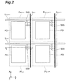
- Fig. 2 is a partially enlarged plan view of the solid-state imaging device 1.
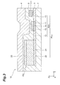
- Fig. 3 is a side sectional view showing a section taken along a line I-I of Fig. 2 .
- an XYZ orthogonal coordinate system is also shown for easy understanding.
- the solid-state imaging device 1 includes a glass substrate 7, a photodetecting section 10 fabricated on a principal surface of the glass substrate 7, a vertical shift register section 40a (first vertical shift register section), and a vertical shift register section 40b (second vertical shift register section). Moreover, the solid-state imaging device 1 includes a signal connecting section 20 disposed outside of the glass substrate 7.
- the signal connecting section 20 is composed of, for example, a plurality of C-MOS IC chips 20a electrically connected with the photodetecting section 10.
- the two vertical shift register sections 40a and 40b are respectively disposed on opposite sides of the photodetecting section 10.
- the photodetecting section 10 and the vertical shift register sections 40a and 40b may be respectively provided on separate glass substrates 7. Further, the signal connecting section 20 may be provided on the glass substrate 7 with the photodetecting section 10 and the vertical shift register sections 40a and 40b.
- the photodetecting section 10 is composed of M ⁇ N pixels two-dimensionally arrayed in M rows and N columns.
- the pixel P m,n shown in Fig. 2 is a pixel located on the m-th row and the n-th column.
- m is an integer not less than 1 and not more than M
- n is an integer not less than 1 and not more than N.
- M and N are each an even number not less than 2.
- the column direction is coincident with the X-axis direction
- the row direction is coincident with the Y-axis direction.
- Each of the plurality of pixels P 1,1 to P M,N included in the photodetecting section 10 includes a photodiode PD and a readout switch SW 1 .
- One end (one current terminal) of the readout switch SW 1 is connected to the photodiode PD. Further, the other end (the other current terminal) of the readout switch SW 1 is connected to a corresponding readout wiring line (for example, in the case of the pixel P m,n , an n-th column readout wiring line L O,n ). A control terminal of the readout switch SW 1 is connected to a corresponding row selection wiring line (for example, in the case of the pixel P m,n , an m-th row selection wiring line L V,m ).
- a silicon film 3 is provided over the entire surface on the glass substrate 7.
- the photodiode PD, the readout switch SW 1 , and the n-th column readout wiring line L O,n are formed on the surface of the silicon film 3.
- the photodiode PD, the readout switch SW 1 , and the n-th column readout wiring line L O,n are covered with an insulating layer 5, and on the insulating layer 5, a scintillator 4 is provided so as to cover the entire surface of the glass substrate 7.
- the photodiode PD is constructed containing, for example, amorphous silicon.
- the photodiode PD of the present embodiment includes an n-type semiconductor layer 21 made of n-type polycrystalline silicon, an i-type semiconductor layer 22 made of i-type amorphous silicon provided on the n-type semiconductor layer 21, and a p-type semiconductor layer 23 made of p-type amorphous silicon provided on the i-type semiconductor layer 22.
- the readout switch SW 1 is an FET formed of polycrystalline silicon, and includes a channel region 11, a source region 12 disposed along one side surface of the channel region 11, a drain region 13 disposed along the other side surface of the channel region 11, and a gate insulating film 14 and a gate electrode 15 formed on the channel region 11.
- the n-th column readout wiring line L O,n is made of metal.
- the scintillator 4 generates scintillation light in response to incident X-rays to convert an X-ray image into an optical image, and outputs the optical image to the photodetecting section 10.
- the polycrystalline silicon that forms the readout switch SW 1 is more preferably low-temperature polycrystalline silicon.
- the low-temperature polycrystalline silicon is polycrystalline silicon that is formed at a process temperature of 100 to 600°C. Because the range of the process temperature of 100 to 600°C is a temperature range where alkali-free glass can be used as a substrate, it becomes possible to produce a large-area photodetecting section 10 on a glass substrate.
- the alkali-free glass is, for example, sheet glass having a thickness of 0.3 to 1.2mm, and used as so-called glass for substrates.
- the alkali-free glass contains little alkali, has a low coefficient of expansion and high heat resistance, and has stable characteristics.
- the mobility of a low-temperature polycrystalline silicon-based device is 10 to 600cm 2 /Vs, and can be made greater than the mobility (0.3 to 1.0cm 2 /Vs) of amorphous silicon. That is, the on-resistance can be lowered.
- the pixel P m,n as shown in Fig. 3 is produced, for example, by the following process.
- amorphous silicon is film-formed on the glass substrate 7.
- the film forming method for example, plasma CVD is favorable.
- the amorphous silicon film is sequentially irradiated with laser beams by excimer laser annealing to make the entire surface of the amorphous silicon film into polycrystalline silicon.
- a silicon film 3 is formed.
- a SiO 2 film to serve as a gate insulating film 14 is formed on a partial region of the silicon film 3 being a polycrystalline silicon layer
- a gate electrode 15 is formed thereon.
- ions are implanted into regions to be the source region 12 and the drain region 13.
- ions are implanted into a region to be the pixel P m,n in the silicon film 3 so as to become n-type, i-type and p-type amorphous silicon layers (i.e. an i-type semiconductor layer 22 and a p-type semiconductor layer 23) are deposited thereon in order to form a PIN photodiode PD.
- a passivation film to serve as the insulating layer 5 is formed.
- the signal connecting section 20 shown in Fig. 1 holds voltage values according to the amounts of charges output from the respective pixels P 1,1 to P M,N of the photodetecting section 10, and outputs the held voltage values successively row by row.
- the signal connecting section 20 of the present embodiment has a normal operation mode and a binning operation mode. In the normal operation mode, the signal connecting section converts charges sent from the pixels P of respective rows into voltage values on a one-row basis, and sequentially outputs these voltage values. Moreover, in the binning operation mode, the signal connecting section converts charges sent from the pixels P of respective rows into voltage values on a two-row basis, and sequentially outputs these voltage values.
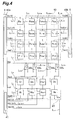
- Fig. 4 is a diagram showing an internal configuration of the solid-state imaging device 1.
- the photodetecting section 10 consists of M ⁇ N pixels P 1,1 to P M,N arrayed two-dimensionally in M rows and N columns.
- Each of the M row selection wiring lines L V,1 to L V,M is constructed by a single wiring line extending from the first column to the N-th column.
- the N pixels P m,1 to P m,N of the m-th row are connected to the vertical shift register sections 40a and 40b via the m-th row selection wiring line L V,m . Also, as shown in Fig.
- the vertical shift register section 40a is connected to one end of the m-th row selection wiring line L V,m
- the vertical shift register section 40b is connected to the other end of the m-th row selection wiring line L V,m .
- the two vertical shift register sections 40a and 40b are both included in a controlling section 6.
- the signal connecting section 20 includes N integration circuits S 1 to S N and N holding circuits H 1 to H N provided for each column.
- the integration circuits S 1 to S N and the holding circuits H 1 to H N are connected in series with each other for each column.
- the respective integration circuits S 1 to S N have a common configuration.
- the respective holding circuits H 1 to H N have a common configuration.
- N/2 horizontal binning changeover switches SW 4 are provided for every two columns.
- An output terminal of each of the M pixels P 1,n to P M,n contained in each of the odd-numbered columns is connected, via the n-th column readout wiring line L O,n , to an input terminal of the integration circuit S n of the signal connecting section 20.
- an output end of each of the M pixels P 1,n to P M,n contained in each of the even-numbered columns is connected to an input terminal of the horizontal binning changeover switch SW 4 .
- the horizontal binning changeover switch SW 4 has two output terminals, and one output terminal is connected to the integration circuit S n of the even-numbered column concerned, and the other output terminal is connected to the integration circuit S n-1 of an adjacent odd-numbered column.
- Control terminals of the N/2 horizontal binning changeover switches SW 4 are connected to the controlling section 6 via a common binning changeover wiring line L B .
- the integration circuits S 1 to S N have input terminals connected to the column readout wiring lines L O,1 to L O,N , respectively, and accumulate charges input to the input terminals, and output voltage values according to the accumulated charge amounts from output terminals to the holding circuits H 1 to H N .
- the integration circuits S 1 to S N are connected to the controlling section 6 via a common reset wiring line L R .
- the holding circuits H 1 to H N have input terminals connected to the output terminals of the integration circuits S 1 to S N , respectively, hold voltage values input to the input terminals, and output the held voltage values from output terminals to a voltage output wiring line L out .
- the holding circuits H 1 to H N are connected to the controlling section 6 via a common hold wiring line L H .
- each of the holding circuits H 1 to H N is connected to a horizontal shift register section 41 of the controlling section 6 via each of the first column selection wiring line L S,1 to the N-th column selection wiring line L S,N .
- the vertical shift register sections 40a and 40b of the controlling section 6 output an m-th row selection control signal Vsel(m) to the m-th row selection wiring line L V,m to provide this m-th row selection control signal Vsel(m) to each of the N pixels P m,1 to P m,N of the m-th row.
- M row selection control signals Vsel(1) to Vsel(M) sequentially take significant values.
- the horizontal shift register section 41 of the controlling section 6 outputs column selection control signals Hshift(1) to Hshift(N) to the column selection wiring lines L S,1 to L S,N to provide these column selection control signals Hshift(1) to Hshift(N) to the holding circuits H 1 to H N .
- the column selection control signals Hshift(1) to Hshift(N) also sequentially take significant values.
- the controlling section 6 outputs a reset control signal Reset to the reset wiring line L R to provide this reset control signal Reset to each of the N integration circuits S 1 to S N .
- the controlling section 6 outputs a hold control signal Hold to the hold wiring line L H to provide this hold control signal Hold to each of the N holding circuits H 1 to H N .
- the controlling section 6 outputs a horizontal binning control signal Hbin to the binning changeover wiring line L B to provide this horizontal binning control signal Hbin to each of the N/2 horizontal binning changeover switches SW 4 .
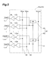
- Fig. 5 is a circuit diagram showing a configuration of the vertical shift register sections 40a, 40b.
- the vertical shift register section 40a, 40b of the present embodiment includes a shift register array 42, M logic circuits LO 1 to LO M , a first binning selection wiring line 45, and a second binning selection wiring line 46.
- the shift register array 42 is composed of M/2 shift register circuits 43 connected in series. These shift register circuits 43 are provided, for the M row selection wiring lines L V,1 to L V,M , one each for every two row selection wiring lines. In Fig. 5 , one shift register circuit 43 is disposed corresponding to two row selection wiring lines L V,1 and L V,2 , and one shift register circuit 43 is disposed corresponding to two row selection wiring lines L V,M-1 to L V,M .
- the shift register circuit 43 is composed of a plurality of FETs formed of a semiconductor material containing polycrystalline silicon, having the similar structure as that of the readout switch SW 1 shown in Fig. 3 . Each shift register circuit 43 is connected with a clock wiring line L C , and a clock signal Vclock with a given period is provided from the clock wiring line L C to each shift register circuit 43.
- the first binning selection wiring line 45 when reading out charges from the respective pixels P 1 , 1 to P M,N , provides a first binning control signal Vbin 1 to select one row selection wiring line L V,1 , L V,3 ..., L V,M-1 of each two row selection wiring lines connected to each shift register circuit 43.
- the second binning selection wiring line 46 when reading out charges from the respective pixels P 1,1 to P M,N , provides a second binning control signal Vbin 2 to select the other row selection wiring line L V,2 , L V,4 ..., L V,M of each two row selection wiring lines connected to each shift register circuit 43.
- the vertical shift register sections 40a and 40b by controlling the timing of the first binning control signal Vbin 1 and the second binning control signal Vbin 2 , realize a normal operation mode for successively selecting the two row selection wiring lines and a binning operation mode for simultaneously selecting the two row selection wiring lines. That is, in the normal operation mode, the first binning control signal Vbin 1 and the second binning control signal Vbin 2 successively take significant values. On the other hand, in the binning operation mode, the first binning control signal Vbin 1 and the second binning control signal Vbin 2 simultaneously take significant values.
- the M logic circuits LO 1 to LO M correspond one-to-one to the M row selection wiring lines L V,1 to L V,M .
- An output terminal of each of the logic circuits LO 1 to LO M is connected, via a buffer 44 provided for each row, to each of the row selection wiring lines L V,1 to L V,M .
- one-side input terminals of the respective logic circuits LO 1 to LO M are alternately connected to the first binning selection wiring line 45 and the second binning selection wiring line 46.
- the first binning selection wiring line 45 is connected to one input terminal of the logic circuit LO m connected to one row selection wiring line L V,m of the two row selection wiring lines L V,m and L V,m+1 corresponding to one shift register circuit 43.
- the second binning selection wiring line 46 is connected to one input terminal of the logic circuit LO m+1 connected to the other row selection wiring line L V,m+1 .
- one-side input ends of M/2 logic circuits LO 1 , LO 3 , ..., LO M-1 connected to one of each two row selection wiring lines corresponding to each shift register circuit 43 are connected with the first binning selection wiring line 45, and one-side input ends of the remaining M/2 logic circuits LO 2 , LO 4 , ..., LO M connected to the other are connected with the second binning selection wiring line 46.
- an output terminal of the shift register circuit 43 provided corresponding to a row selection wiring line to which the logic circuit concerned is connected is connected to the other input terminal of each of the logic circuits LO 1 to LO M .
- the output terminal of the shift register circuit 43 provided corresponding to the row selection wiring lines L V,1 and L V,2 is connected to the-other-side input terminals of the logic circuits LO M-1 and LO M .
- the output terminal of the shift register circuit 43 provided corresponding to the row selection wiring lines L V,M-1 and L V,M is connected.
- Each of the M logic circuits LO 1 to LO M when the first binning control signal Vbin 1 or the second binning control signal Vbin 2 and an output signal from the shift register circuit 43 corresponding to the logic circuit concerned both have significant values, outputs each of the row selection control signals Vsel(1) to Vsel(M) so as to close the readout switch SW 1 .
- the significant values of the first binning control signal Vbin 1 and the second binning control signal Vbin 2 are low level and the significant value of an output signal from the shift register circuit 43 is low level
- the M logic circuits LO 1 to LO M output negative OR (NOR) of the first binning control signal Vbin 1 or the second binning control signal Vbin 2 and the output signal from the shift register circuit 43.
- the logic circuits LO 1 to LO M are illustrated with the symbols standing for NOR circuits in Fig. 5 , the logic circuits LO 1 to LO M may be constructed by combination of other various logic circuits.
- Fig. 6 is a diagram showing a circuit configuration of each of the pixels P m,n and P m,n+1 , integration circuits S n and S n+1 , and holding circuits H n and H n+1 of the solid-state imaging device 1.
- circuit diagrams of the pixels P m,n and P m,n+1 are shown as representatives of the M ⁇ N pixels P 1,1 to P M,N
- circuit diagrams of the integration circuits S n and S n+1 are shown as representatives of the N integration circuits S 1 to S N
- circuit diagrams of the holding circuits H n and H n+1 are shown as representatives of the N holding circuits H 1 to H N .
- a circuit portion relating to the pixel P m,n on the m-th row and the n-th column and the n-th column readout wiring line L O,n and a circuit portion relating to the pixel P m,n+1 on the m-th row and the (n+1)-th column and the (n+1)-th column readout wiring line L O,n+1 are shown.
- the pixels P m,n and P m,n+1 include photodiodes PD and readout switches SW 1 .
- the anode terminals of the photodiodes PD are grounded, and the cathode terminals are connected with the corresponding readout wiring lines L O,n and L O,n+1 , respectively, via the readout switches SW 1 .
- Each photodiode PD generates charge of an amount according to an incident light intensity, and accumulates the generated charge in a junction capacitance section.
- Each readout switch SW 1 is provided with an m-th row selection control signal Vsel(m) via the m-th row selection wiring line L V,m from the vertical shift register section 40a or 40b.
- the m-th row selection control signal Vsel(m) instructs an opening and closing operation of the readout switch SW 1 in each of the N pixels P m,1 to P m,N of the m-th row in the photodetecting section 10.
- one readout wiring line L O,n+1 of the two readout wiring lines L O,n and L O,n+1 is connected with a horizontal binning changeover switch SW 4 .
- the horizontal binning changeover switch SW 4 is provided with a horizontal binning control signal Hbin via the horizontal binning changeover wiring line L B from the controlling section 6.
- the horizontal binning control signal Hbin instructs a switching operation of the N/2 horizontal binning changeover switches SW 4 .
- the horizontal binning changeover switch SW 4 when the horizontal binning control signal Hbin has a non-significant value (for example, low level), connects the readout wiring line L O,n+1 and the integration circuit S n+1 . At this time, a charge flowing through the readout wiring line L O,n+1 is output to the integration circuit S n+1 , and a charge flowing through the readout wiring line L O,n is output to the integration circuit S n (normal operation mode).
- the horizontal binning changeover switch SW 4 when the horizontal binning control signal Hbin has a significant value (for example, high level), connects the readout wiring line L O,n+1 and the integration circuit S n . At this time, a charge flowing through the readout wiring line L O,n+1 is output to the integration circuit S n together with a charge flowing through the readout wiring line L O,n (binning operation mode).
- the integration circuits S n and S n+1 include amplifiers A 2 , integrating capacitive elements C 21 serving as feedback capacitance sections, and discharge switches SW 21 .
- Each integrating capacitive element C 21 and each discharge switch SW 21 are connected in parallel with each other, and provided between an input terminal and an output terminal of each amplifier A 2 .
- the input terminals of the amplifiers A 2 are connected with the corresponding readout wiring lines L O,n and L O,n+1 , respectively.
- Each discharge switch SW 21 is provided with a reset control signal Reset via the reset wiring line L R from the controlling section 6.
- the reset control signal Reset instructs an opening and closing operation of the discharge switch SW 21 in each of the N integration circuits S 1 to S N .
- the holding circuits H n and H n+1 include input switches SW 31 , output switches SW 32 , and holding capacitive elements C 3 .
- One-side ends of the holding capacitive elements C 3 are grounded.
- The-other-side ends of the holding capacitive elements C 3 are connected to the output terminals of the corresponding integration circuits S n and S n+1 via the input switches SW 31 , and connected with the voltage output wiring line L out via the output switches SW 32 .
- Each input switch SW 31 is provided with a hold control signal Hold via the hold wiring line L H from the controlling section 6.
- the hold control signal Hold instructs an opening and closing operation of the input switch SW 31 in each of the N holding circuits H 1 to H N .
- the output switch SW 32 of the holding circuit H n is provided with an n-th column selection control signal Hshift(n) passed through the n-th column selection wiring line L S,n from the controlling section 6.
- the output switch SW 32 of the holding circuit H n+1 is provided with an (n+1)-th column selection control signal Hshift(n+1) passed through the (n+1)-th column selection wiring line L S,n+1 from the controlling section 6.
- the selection control signals Hshift(1) to Hshift(N) instruct an opening and closing operation of the output switches SW 32 of the respective holding circuits H 1 to H N .
- each input switch SW 31 switches from a closed state to an open state, and a voltage value being input to the input terminal at this time is held in each holding capacitive element C 3 .
- the output switch SW 32 of the holding circuit H n closes, and the voltage value held in the holding capacitive element C 3 of the holding circuit H n is output to the voltage output wiring line L out .
- the output switch SW 32 of the holding circuit H n+1 closes, and the voltage value held in the holding capacitive element C 3 of the holding circuit H n+1 is output to the voltage output wiring line L out .
- the controlling section 6 when outputting a voltage value according to a received light intensity in each of the N pixels P m,1 to P m,N of the m-th row in the photodetecting section 10, instructs opening after closing for a predetermined period of the discharge switch SW 21 in each of the N integration circuits S 1 to S N by a reset control signal Reset, and then instructs opening after closing for a predetermined period of the readout switch SW 1 in each of the N pixels P m,1 to P m,N of the m-th row in the photodetecting section 10 by an m-th row selection control signal Vsel(m).
- the controlling section 6 instructs switching of the input switch SW 31 in each of the N holding circuits H 1 to H N from a closed state to an open state by a hold control signal Hold. Then, the controlling section 6 instructs sequential closing of the output switches SW 32 of the respective N holding circuits H 1 to H N for a given period by column selection control signals Hshift(1) to Hshift(N). The controlling section 6 performs such control as in the above for the respective rows in sequence.
- the controlling section 6 controls an opening and closing operation of a readout switch SW 1 in each of the M ⁇ N pixels P 1,1 to P M,N in the photodetecting section 10, and controls a holding operation and an output operation of a voltage value in the signal connecting section 20. Accordingly, the controlling section 6 causes a voltage value according to the amount of charge generated in the photodiode PD of each of the M ⁇ N pixels P 1,1 to P M,N in the photodetecting section 10 to be repeatedly output as frame data from the signal connecting section 20.
- Fig. 7 is a timing chart for explaining a normal operation of the solid-state imaging device 1 according to the present embodiment.
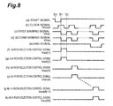
- Fig. 8 is a timing chart for explaining a binning operation of the solid-state imaging device 1 according to the present embodiment.
- each of the start signal, the first binning signal, the second binning signal, and the end signal has a non-significant value (high level).
- each of the M row selection control signals Vsel(1) to Vsel(M) has a non-significant value (low level).
- the start signal to be output from the controlling section 6 takes a significant value (low level).
- the first binning signal Vbin 1 in response thereto takes a significant value (low level) for a period from the time t 11 to the time t 12 .
- an output signal from the first-stage shift register circuit 43 takes a significant value (low level).
- the first row selection control signal Vsel(1) to be output from the logic circuit LO 1 to the first row selection wiring line L V,1 takes a significant value (high level) for the period from the time t 11 to the time t 12 , and the readout switch SW 1 in each of the N pixels P 1,1 to P 1,N of the first row in the photodetecting section 10 reaches a connected state.
- Charges generated in the photodiodes PD of the respective N pixels P 1 , 1 to P 1,N and accumulated in the junction capacitance sections are output to the integration circuits S 1 to S N through the readout switches SW 1 and the column readout wiring lines L O,1 to L O,N , and accumulated in the integrating capacitive elements C 21 . From the integration circuits S 1 to S N , voltages of the magnitudes according to the amounts of charges accumulated in the integrating capacitive elements C 21 are output.
- the input switches SW 31 of the N holding circuits H 1 to H N reach a connected state, and the magnitudes of voltages output from the integration circuits S 1 to S N are held by the holding circuits H 1 to H N .
- the column selection control signals Hshift(1) to Hshift(N) to be output to the column selection wiring lines L S,1 to L S,N from the horizontal shift register section 41 sequentially take significant values (high level) for a given period, and the output switches SW 32 of the respective N holding circuits H 1 to H N sequentially reach a connected state for the given period, so that the voltage values held in the holding capacitive elements C 3 of the respective holding circuits H 1 to H N are sequentially output to the voltage output wiring line L out through the output switches SW 32 ⁇
- the clock signal Vclock falls, and the second binning signal Vbin 2 in response thereto takes a significant value (low level) for a period from the time t 13 to the time t 14 after the time t 12 .
- the output signal from the first-stage shift register circuit 43 is maintained at a significant value (low level).
- the second row selection control signal Vsel(2) to be output from the logic circuit LO 2 to the second row selection wiring line L V,2 takes a significant value (high level) for the period from the time t 13 to the time t 14 , and the readout switch SW 1 in each of the N pixels P 2,1 to P 2,N of the second row in the photodetecting section 10 reaches a connected state.
- Charges generated in the photodiodes PD of the respective N pixels P 2,1 to P 2,N and accumulated in the junction capacitance sections are output to the integration circuits S 1 to S N , and accumulated in the integrating capacitive elements C 21 . Subsequently, by the same operation as the operation in the case of the first row, voltage values of the magnitudes according to these charges are sequentially output to the voltage output wiring line L out .
- the same operation is performed for the third row to the M-th row, so that frame data indicating an image captured in one time imaging is obtained. Also, when the operation ends with respect to the M-th row, the same operation is again performed in a range from the first row to the M-th row, and frame data indicating a next image is obtained.
- each of the start signal, the first binning signal, the second binning signal, and the end signal has a non-significant value (high level).
- each of the M row selection control signals Vsel(1) to Vsel(M) has a non-significant value (low level).
- the start signal to be output from the controlling section 6 takes a significant value (low level).
- the first binning signal Vbin 1 and the second binning signal Vbin 2 in response thereto take significant values (low level) for a period from the time t 21 to the time t 22 .
- an output signal from the first-stage shift register circuit 43 takes a significant value (low level).
- the first row selection control signal Vsel(1) to be output from the logic circuit LO 1 to the first row selection wiring line L V,1 and the second row selection control signal Vsel(2) to be output from the logic circuit LO 2 to the second row selection wiring line L V,2 take significant values (high level) for the period from the time t 21 to the time t 22 , and the readout switches SW 1 in the N pixels P 1,1 to P 1,N of the first row and the N pixels P 2,1 to P 2,N of the second row in the photodetecting section 10 reach a connected state.
- the input switches SW 31 of the N holding circuits H 1 to H N reach a connected state, and the magnitudes of voltages output from the integration circuits S 1 to S N are held by the holding circuits H 1 to H N .
- the column selection control signals Hshift(1), Hshift(3), ..., Hshift(N-1) sequentially take significant values (high level) for a given period, and the output switches SW 32 of respective N/2 holding circuits H 1 , H 3 , ..., H N-1 sequentially reach a connected state for the given period, so that the voltage values held in the holding capacitive elements C 3 of the respective holding circuits H 1 , H 3 , ..., H N-1 are sequentially output to the voltage output wiring line L out through the output switches SW 32 ⁇
- the same operation is performed for the third row to the M-th row, so that frame data indicating an image captured in one time imaging is obtained. Also, when the operation ends with respect to the M-th row, the same operation is again performed in a range from the first row to the M-th row, and frame data indicating a next image is obtained.
- the solid-state imaging device 1 By the solid-state imaging device 1 according to the present embodiment described in the above, the following effects are obtained. That is, by the solid-state imaging device 1, as a result of the vertical shift register sections 40a and 40b having the configuration shown in Fig. 5 , both the normal operation and binning operation can be favorably realized. Moreover, because the shift register circuits 43 of the vertical shift register sections 40a, 40b are provided for every two row selection wiring lines, the vertical shift register sections 40a, 40b can be made smaller than that of a conventional solid-state imaging device for which shift register circuits are disposed for each row. Particularly, in the solid-state imaging device 1 of the present embodiment, because the shift register circuits 43 are formed of a semiconductor material containing polycrystalline silicon, such an effect is more remarkable.
- each of the M row selection wiring lines L V,1 to L V,M may be constructed by a single wiring line extending from the first column to the N-th column.
- each of the vertical shift register sections 40a and 40b provides a row selection control signal Vsel to each of both ends of the M row selection wiring lines L V,1 to L V,M .
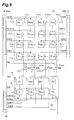
- FIG. 9 is a diagram showing the internal configuration of a solid-state imaging device of the present modification.
- the difference in configuration between the present modification and the above-mentioned embodiment is in the configuration of row selection wiring lines.
- each of the M row selection wiring lines L V,1 to L V,M has a first part extending from the pixel P m,1 to the pixel P m,Na (provided that Na is an integer not less than 2 and not more than N-1) and a second part extending from the pixel P m,Na+1 to the pixel P m,N , and these parts are electrically separated from each other.
- one part (pixels P m,1 to P m,Na ) of the N pixels P m,1 to P m,N of the m-th row is connected to one vertical shift register section 40a via the first part of the m-th row selection wiring line L V,m .
- the other part (pixels P m,Na+1 to P m,N ) of the N pixels P m,1 to P m,N of the m-th row is connected to the other vertical shift register section 40b via the second part of the m-th row selection wiring line L V,m .
- the two vertical shift register sections 40a and 40b are both included in the controlling section 6.
- the vertical shift register section 40a of the controlling section 6 outputs an m-th row selection control signal Vsel(m) to the m-th row selection wiring line L V,m to provide this m-th row selection control signal Vsel(m) to each of the Na pixels P m,1 to P m,Na of the m-th row.
- the vertical shift register section 40b outputs an m-th row selection control signal Vsel(m) to the m-th row selection wiring line L V,m to provide this m-th row selection control signal Vsel(m) to each of the (N-Na) pixels P m,Na+1 to P m,N of the m-th row.
- M row selection control signals Vsel(1) to Vsel(M) sequentially take significant values.
- a delay in the row selection control signals Vsel(1) to Vsel(M) to be provided for the large-area photodetecting section 10 can be effectively suppressed.
- the solid-state imaging device by the present invention is not limited to the embodiments described above, and various other modifications can be made.
- description has been given of an example in which the present invention is applied to a solid-state imaging device formed by film-forming of polycrystalline silicon or amorphous silicon on a glass substrate, but the present invention is not limited to such a configuration, and can also be applied to, for example, a solid-state imaging element that is fabricated on a monocrystalline silicon substrate.
- the solid-state imaging device of the above-mentioned embodiment includes a light receiving section consisting of M ⁇ N (M is an even number not less than 2, N is an integer not less than 2) pixels each including a photodiode and a readout switch connected at one end to the photodiode that are arrayed two-dimensionally in M rows and N columns, M row selection wiring lines arranged for each row, and connected to control terminals of the readout switches included in the pixels of corresponding rows, and a vertical shift register section for providing row selection control signals for controlling opening and closing of the readout switches to the M row selection wiring lines, the vertical shift register section includes a shift register array including M/2 shift register circuits formed of a semiconductor material containing polycrystalline silicon, and disposed for every two row selection wiring lines, M logic circuits for outputting the row selection control signals respectively to the M row selection wiring lines, a first binning selection wiring line for providing one-side input terminals of M/2 logic circuits connected to one of each two row selection wiring lines with a first binning control signal
- the solid-state imaging device may be arranged such that each of the M row selection wiring lines is constructed by a single wiring line extending from the first column to the N-th column, and the solid-state imaging device includes a first vertical shift register section for providing the row selection control signals to one-side ends of the M row selection wiring lines, and a second vertical shift register section for providing the row selection control signals to the-other-side ends of the M row selection wiring lines.
- the solid-state imaging device may be arranged such that the M row selection wiring lines include first parts connected to control terminals of the readout switches included in the pixels of the first column through the Na-th column (Na is an integer not less than 2 and not more than N-1) out of the N columns and second parts connected to control terminals of the readout switches included in the pixels of the (Na+1)-th column through the N-th column out of the N columns, and the solid-state imaging device includes a first vertical shift register section for providing the row selection control signals to the first parts of the M row selection wiring lines, and a second vertical shift register section for providing the row selection control signals to the second parts of the M row selection wiring lines. Accordingly, a delay in the row selection control signals to be provided for the large-area photodetecting section can be suppressed.
- the present invention can be applied as a solid-state imaging device which allows realizing a vertical binning operation by a small vertical shift register.
- 1 - solid-state imaging device 6 - controlling section, 10 - photodetecting section, 20 - signal connecting section, 40a, 40b - vertical shift register section, 43 - shift register circuit, 45 - first binning selection wiring line, 46 - second binning selection wiring line, PD - photodiode, P - pixel, SW 1 - readout switch, SW 31 - input switch, SW 32 - output switch, SW 4 - horizontal binning changeover switch, S 1 to S N - integration circuit, H 1 to H N - holding circuit, C 21 - integrating capacitive element, A 2 - amplifier, L B - horizontal binning changeover wiring line, L O,1 to L O,N - column readout wiring line, L V,1 to L V,M - row selection wiring line.
Landscapes
- Engineering & Computer Science (AREA)
- Multimedia (AREA)
- Signal Processing (AREA)
- Transforming Light Signals Into Electric Signals (AREA)
- Solid State Image Pick-Up Elements (AREA)
- Health & Medical Sciences (AREA)
- Toxicology (AREA)
Abstract
Description
- The present invention relates to a solid-state imaging device.
-
Patent Document 1 describes a device for which optical sensors are arrayed in the row direction and column direction. The device described in this document includes a shift register array that supplies vertical scanning signals, switches for connecting neighboring vertical signal wiring lines to each other, and a shift register array that controls the opening and closing of the switches, and enables a vertical binning operation by closing the above-mentioned switch. -
- Patent Document 1: Japanese Patent Application Laid-Open No.
2001-189891 - In recent years, for example, for solid-state imaging elements such as two-dimensional flat panel image sensors to be used for medical purposes (such as dental radiography), wider photodetecting surfaces have been demanded. However, if photodetecting sections (photodiode arrays) are fabricated on monocrystalline silicon wafers as in prior solid-state imaging elements, the extent of photodetecting surfaces of the solid-state imaging elements is limited due to the size of the monocrystalline silicon wafers that are at most 12 inches in diameter. Therefore, the present inventors have studied, for example, a technique of forming a film of polycrystalline silicon on an insulating substrate such as a glass substrate, and forming photodiodes and other electronic components such as transistors on the surface of the polycrystalline silicon. Providing solid-state imaging elements with such structures enables making the photodetecting surfaces remarkably wide as compared with those of conventional solid-state imaging elements formed with use of monocrystalline silicon wafers.
- Meanwhile, for a solid-state imaging element, it is sometimes desired to output data of a plurality of adjacent pixels collectively, a so-called binning operation. For example, when the solid-state imaging element is used for medical purposes, performing a binning operation enables quickly identifying a region that is desired to be observed, observation through a moving image, and the like. Also, binning methods include a method of collectively reading out charges from a plurality of adjacent pixels and a method of generating digital data of each pixel by a normal operation, and then adding and outputting the digital data of a plurality of adjacent pixels. Of these, the method of collectively reading out charges from a plurality of pixels is preferable because this allows making the frame rate faster than that by the method of adding and outputting the digital data of a plurality of pixels.
- However, when charges from a plurality of adjacent pixels are collectively read out, if a vertical shift register that is used for a normal operation is added with a circuit for making the same correspond to a vertical binning operation, the vertical shift register is increased in size. In particular, when vertical shift registers are formed on the surface of polycrystalline silicon film-formed on an insulating substrate, it is difficult to use such a microfabrication process as used when forming the same on a monocrystalline silicon wafer, and the only outcome is a relatively low degree of integration. Accordingly, as a result of the addition of a circuit for vertical binning as described above, the increase in size of the vertical shift register becomes more remarkable.
- It is therefore an object of the present invention to provide a solid-state imaging device which allows realizing a vertical binning operation by a small vertical shift register.
- In order to solve the above-described problem, a solid-state imaging device according to the present invention includes a photodetecting section having M×N (M is an even number not less than 2, N is an integer not less than 2) pixels each including a photodiode and a readout switch connected at one end to the photodiode that are arrayed two-dimensionally in M rows and N columns, M row selection wiring lines arranged for each row, and connected to control terminals of the readout switches included in the pixels of corresponding rows, and a vertical shift register section for providing row selection control signals for controlling opening and closing of the readout switches to the M row selection wiring lines, the vertical shift register section includes a shift register array including M/2 shift register circuits formed of a semiconductor material containing polycrystalline silicon, and disposed for every two row selection wiring lines, M logic circuits for outputting the row selection control signals respectively to the M row selection wiring lines, a first binning selection wiring line for providing one-side input terminals of M/2 logic circuits connected to one of each two row selection wiring lines with a first binning control signal for selecting the one row selection wiring line, and a second binning selection wiring line for providing one-side input terminals of M/2 logic circuits connected to the other of each two row selection wiring lines with a second binning control signal for selecting the other row selection wiring line, and in the device, to the-other-side input terminal of each of the M logic circuits, an output terminal of the shift register circuit corresponding to the row selection wiring line connected to the logic circuit is connected, each of the M logic circuits, when the first binning control signal or the second binning control signal and an output signal from the shift register circuit both have significant values, outputs the row selection control signal so as to close the readout switch, and the vertical shift register section has a normal operation mode for successively selecting the two row selection wiring lines and a binning operation mode for simultaneously selecting the two row selection wiring lines, by controlling the timings at which the first binning control signal and the second binning control signal take significant values.
- This solid-state imaging device can operate, for example, as follows. First, in the normal operation mode, one input terminal of a logic circuit connected to one of the first two row selection wiring lines is provided with a significant value of a first binning control signal. Simultaneously, to the other input terminal of the logic circuit, a significant value of an output signal from the first-stage shift register circuit is provided. Accordingly, the readout switches of the respective pixels of the first row close due to a row selection control signal output from the logic circuit, so that charges are output from the photodiodes of the respective pixels of the first row. Next, the significant value of the output signal from the first-stage shift register circuit is maintained, while one input terminal of a logic circuit connected to the other of the first two row selection wiring lines is provided with a significant value of a second binning control signal. Accordingly, the readout switches of the respective pixels of the second row close due to a row selection control signal output from the logic circuit, so that charges are output from the photodiodes of the respective pixels of the second row. Subsequently, the same operation is performed also for the next two row selection wiring lines, and thereafter, the same operation is performed until the M-th row.
- On the other hand, in the binning operation mode, one input terminal of a logic circuit connected to one of the first two row selection wiring lines is provided with a significant value of a first binning control signal. Simultaneously, one input terminal of a logic circuit connected to the other of the two row selection wiring lines is provided with a significant value of a second binning control signal. Moreover, simultaneously with these operations, to the-other-side input terminals of the logic circuits, a significant value of an output signal from the first-stage shift register circuit is provided. Accordingly, the readout switches of the respective pixels of the first row and the second row close due to row selection control signals output from the two logic circuits connected to the two row selection wiring lines, so that charges are collectively output from the photodiodes of the respective pixels of the first row and the second row.
- Thus, by the solid-state imaging device described above, both the normal operation and vertical binning operation can be favorably realized. Moreover, because the shift register circuits of the vertical shift register section are provided for every two row selection wiring lines, the vertical shift register section can be made smaller than that of a conventional solid-state imaging device for which shift register circuits are disposed for each row. Particularly, when the shift register circuits are formed of a semiconductor material containing polycrystalline silicon as in the solid-state imaging device of the present invention, such an effect is more remarkable.
- The solid-state imaging device by the present invention allows realizing a vertical binning operation by a small vertical shift register.
-
- [
Fig. 1] Fig. 1 is a plan view showing a solid-state imaging device according to an embodiment. - [
Fig. 2] Fig. 2 is a partially enlarged plan view of the solid-state imaging device. - [
Fig. 3] Fig. 3 is a side sectional view showing a section taken along a line I-I ofFig. 2 . - [
Fig. 4] Fig. 4 is a diagram showing an internal configuration of the solid-state imaging device. - [
Fig. 5] Fig. 5 is a circuit diagram showing a configuration of a vertical shift register section. - [
Fig. 6] Fig. 6 is a diagram showing a circuit configuration of each of the pixels, integration circuits, and holding circuits of the solid-state imaging device. - [
Fig. 7] Fig. 7 is a timing chart for explaining a normal operation of the solid-state imaging device. - [
Fig. 8] Fig. 8 is a timing chart for explaining a binning operation of the solid-state imaging device. - [
Fig. 9] Fig. 9 is a diagram showing another example of the internal configuration of the solid-state imaging device. - Hereinafter, embodiments of a solid-state imaging device according to the present invention will be described in detail with reference to the accompanying drawings. Also, the same components will be denoted with the same reference symbols in the description of the drawings, and overlapping description will be omitted.
- The solid-state imaging device according to the present embodiment is used for, for example, a medical X-ray imaging system, and used particularly for a system for taking X-ray images of the jaw of a subject being tested by imaging modes such as panoramic radiography, cephalography, and CT in dentistry medical treatment. Therefore, the solid-state imaging device of the present embodiment includes thin-film transistors formed by polycrystalline silicon deposited on a large-area glass substrate and photodiodes formed by amorphous silicon deposited thereon, and has a remarkably wide photodetecting area as compared with that of a conventional solid-state imaging device prepared from a monocrystalline silicon wafer.
Fig. 1 to Fig. 3 are views showing a configuration of the solid-state imaging device 1 of the present embodiment.Fig. 1 is a plan view showing the solid-state imaging device 1, andFig. 2 is a partially enlarged plan view of the solid-state imaging device 1. Further,Fig. 3 is a side sectional view showing a section taken along a line I-I ofFig. 2 . Also, inFig. 1 to Fig. 3 , an XYZ orthogonal coordinate system is also shown for easy understanding. - As shown in
Fig. 1 , the solid-state imaging device 1 includes aglass substrate 7, a photodetectingsection 10 fabricated on a principal surface of theglass substrate 7, a verticalshift register section 40a (first vertical shift register section), and a verticalshift register section 40b (second vertical shift register section). Moreover, the solid-state imaging device 1 includes asignal connecting section 20 disposed outside of theglass substrate 7. Thesignal connecting section 20 is composed of, for example, a plurality of C-MOS IC chips 20a electrically connected with the photodetectingsection 10. The two verticalshift register sections section 10. Also, the photodetectingsection 10 and the verticalshift register sections separate glass substrates 7. Further, thesignal connecting section 20 may be provided on theglass substrate 7 with the photodetectingsection 10 and the verticalshift register sections - The photodetecting
section 10 is composed of M×N pixels two-dimensionally arrayed in M rows and N columns. The pixel Pm,n shown inFig. 2 is a pixel located on the m-th row and the n-th column. Here, m is an integer not less than 1 and not more than M, and n is an integer not less than 1 and not more than N. M and N are each an even number not less than 2. Also, inFig. 2 , the column direction is coincident with the X-axis direction, and the row direction is coincident with the Y-axis direction. Each of the plurality of pixels P1,1 to PM,N included in thephotodetecting section 10 includes a photodiode PD and a readout switch SW1. One end (one current terminal) of the readout switch SW1 is connected to the photodiode PD. Further, the other end (the other current terminal) of the readout switch SW1 is connected to a corresponding readout wiring line (for example, in the case of the pixel Pm,n, an n-th column readout wiring line LO,n). A control terminal of the readout switch SW1 is connected to a corresponding row selection wiring line (for example, in the case of the pixel Pm,n, an m-th row selection wiring line LV,m). - As shown in
Fig. 3 , over the entire surface on theglass substrate 7, asilicon film 3 is provided. The photodiode PD, the readout switch SW1, and the n-th column readout wiring line LO,n are formed on the surface of thesilicon film 3. The photodiode PD, the readout switch SW1, and the n-th column readout wiring line LO,n are covered with an insulatinglayer 5, and on the insulatinglayer 5, ascintillator 4 is provided so as to cover the entire surface of theglass substrate 7. The photodiode PD is constructed containing, for example, amorphous silicon. - The photodiode PD of the present embodiment includes an n-
type semiconductor layer 21 made of n-type polycrystalline silicon, an i-type semiconductor layer 22 made of i-type amorphous silicon provided on the n-type semiconductor layer 21, and a p-type semiconductor layer 23 made of p-type amorphous silicon provided on the i-type semiconductor layer 22. Moreover, the readout switch SW1 is an FET formed of polycrystalline silicon, and includes achannel region 11, asource region 12 disposed along one side surface of thechannel region 11, adrain region 13 disposed along the other side surface of thechannel region 11, and agate insulating film 14 and agate electrode 15 formed on thechannel region 11. The n-th column readout wiring line LO,n is made of metal. Thescintillator 4 generates scintillation light in response to incident X-rays to convert an X-ray image into an optical image, and outputs the optical image to thephotodetecting section 10. - The polycrystalline silicon that forms the readout switch SW1 is more preferably low-temperature polycrystalline silicon. The low-temperature polycrystalline silicon is polycrystalline silicon that is formed at a process temperature of 100 to 600°C. Because the range of the process temperature of 100 to 600°C is a temperature range where alkali-free glass can be used as a substrate, it becomes possible to produce a large-
area photodetecting section 10 on a glass substrate. The alkali-free glass is, for example, sheet glass having a thickness of 0.3 to 1.2mm, and used as so-called glass for substrates. The alkali-free glass contains little alkali, has a low coefficient of expansion and high heat resistance, and has stable characteristics. Moreover, the mobility of a low-temperature polycrystalline silicon-based device is 10 to 600cm2/Vs, and can be made greater than the mobility (0.3 to 1.0cm2/Vs) of amorphous silicon. That is, the on-resistance can be lowered. - The pixel Pm,n as shown in
Fig. 3 is produced, for example, by the following process. First, amorphous silicon is film-formed on theglass substrate 7. As the film forming method, for example, plasma CVD is favorable. Next, the amorphous silicon film is sequentially irradiated with laser beams by excimer laser annealing to make the entire surface of the amorphous silicon film into polycrystalline silicon. Thus, asilicon film 3 is formed. Then, after a SiO2 film to serve as agate insulating film 14 is formed on a partial region of thesilicon film 3 being a polycrystalline silicon layer, agate electrode 15 is formed thereon. Then, ions are implanted into regions to be thesource region 12 and thedrain region 13. Subsequently, by carrying out patterning of thesilicon film 3, exposure and etching are repeatedly carried out to form other electrodes and contact holes, etc. Moreover, after ions are implanted into a region to be the pixel Pm,n in thesilicon film 3 so as to become n-type, i-type and p-type amorphous silicon layers (i.e. an i-type semiconductor layer 22 and a p-type semiconductor layer 23) are deposited thereon in order to form a PIN photodiode PD. Subsequently, a passivation film to serve as the insulatinglayer 5 is formed. - The
signal connecting section 20 shown inFig. 1 holds voltage values according to the amounts of charges output from the respective pixels P1,1 to PM,N of thephotodetecting section 10, and outputs the held voltage values successively row by row. Thesignal connecting section 20 of the present embodiment has a normal operation mode and a binning operation mode. In the normal operation mode, the signal connecting section converts charges sent from the pixels P of respective rows into voltage values on a one-row basis, and sequentially outputs these voltage values. Moreover, in the binning operation mode, the signal connecting section converts charges sent from the pixels P of respective rows into voltage values on a two-row basis, and sequentially outputs these voltage values. - Next, a detailed configuration of the solid-
state imaging device 1 according to the present embodiment will be described.Fig. 4 is a diagram showing an internal configuration of the solid-state imaging device 1. As in the above, thephotodetecting section 10 consists of M×N pixels P1,1 to PM,N arrayed two-dimensionally in M rows and N columns. Each of the M row selection wiring lines LV,1 to LV,M is constructed by a single wiring line extending from the first column to the N-th column. The N pixels Pm,1 to Pm,N of the m-th row are connected to the verticalshift register sections Fig. 4 , the verticalshift register section 40a is connected to one end of the m-th row selection wiring line LV,m, and the verticalshift register section 40b is connected to the other end of the m-th row selection wiring line LV,m. The two verticalshift register sections section 6. - The
signal connecting section 20 includes N integration circuits S1 to SN and N holding circuits H1 to HN provided for each column. The integration circuits S1 to SN and the holding circuits H1 to HN are connected in series with each other for each column. The respective integration circuits S1 to SN have a common configuration. Moreover, the respective holding circuits H1 to HN have a common configuration. - Moreover, in the present embodiment, N/2 horizontal binning changeover switches SW4 are provided for every two columns. An output terminal of each of the M pixels P1,n to PM,n contained in each of the odd-numbered columns is connected, via the n-th column readout wiring line LO,n, to an input terminal of the integration circuit Sn of the
signal connecting section 20. Moreover, an output end of each of the M pixels P1,n to PM,n contained in each of the even-numbered columns is connected to an input terminal of the horizontal binning changeover switch SW4. The horizontal binning changeover switch SW4 has two output terminals, and one output terminal is connected to the integration circuit Sn of the even-numbered column concerned, and the other output terminal is connected to the integration circuit Sn-1 of an adjacent odd-numbered column. Control terminals of the N/2 horizontal binning changeover switches SW4 are connected to the controllingsection 6 via a common binning changeover wiring line LB. - The integration circuits S1 to SN have input terminals connected to the column readout wiring lines LO,1 to LO,N, respectively, and accumulate charges input to the input terminals, and output voltage values according to the accumulated charge amounts from output terminals to the holding circuits H1 to HN. The integration circuits S1 to SN are connected to the controlling
section 6 via a common reset wiring line LR. The holding circuits H1 to HN have input terminals connected to the output terminals of the integration circuits S1 to SN, respectively, hold voltage values input to the input terminals, and output the held voltage values from output terminals to a voltage output wiring line Lout. The holding circuits H1 to HN are connected to the controllingsection 6 via a common hold wiring line LH. Moreover, each of the holding circuits H1 to HN is connected to a horizontalshift register section 41 of the controllingsection 6 via each of the first column selection wiring line LS,1 to the N-th column selection wiring line LS,N. - The vertical
shift register sections section 6 output an m-th row selection control signal Vsel(m) to the m-th row selection wiring line LV,m to provide this m-th row selection control signal Vsel(m) to each of the N pixels Pm,1 to Pm,N of the m-th row. In each of the verticalshift register sections shift register section 41 of the controllingsection 6 outputs column selection control signals Hshift(1) to Hshift(N) to the column selection wiring lines LS,1 to LS,N to provide these column selection control signals Hshift(1) to Hshift(N) to the holding circuits H1 to HN. The column selection control signals Hshift(1) to Hshift(N) also sequentially take significant values. - Moreover, the controlling
section 6 outputs a reset control signal Reset to the reset wiring line LR to provide this reset control signal Reset to each of the N integration circuits S1 to SN. The controllingsection 6 outputs a hold control signal Hold to the hold wiring line LH to provide this hold control signal Hold to each of the N holding circuits H1 to HN. The controllingsection 6 outputs a horizontal binning control signal Hbin to the binning changeover wiring line LB to provide this horizontal binning control signal Hbin to each of the N/2 horizontal binning changeover switches SW4. -
Fig. 5 is a circuit diagram showing a configuration of the verticalshift register sections Fig. 5 , the verticalshift register section shift register array 42, M logic circuits LO1 to LOM, a first binningselection wiring line 45, and a second binningselection wiring line 46. - The
shift register array 42 is composed of M/2shift register circuits 43 connected in series. Theseshift register circuits 43 are provided, for the M row selection wiring lines LV,1 to LV,M, one each for every two row selection wiring lines. InFig. 5 , oneshift register circuit 43 is disposed corresponding to two row selection wiring lines LV,1 and LV,2, and oneshift register circuit 43 is disposed corresponding to two row selection wiring lines LV,M-1 to LV,M. Theshift register circuit 43 is composed of a plurality of FETs formed of a semiconductor material containing polycrystalline silicon, having the similar structure as that of the readout switch SW1 shown inFig. 3 . Eachshift register circuit 43 is connected with a clock wiring line LC, and a clock signal Vclock with a given period is provided from the clock wiring line LC to eachshift register circuit 43. - The first binning
selection wiring line 45, when reading out charges from the respective pixels P1,1 to PM,N, provides a first binning control signal Vbin1 to select one row selection wiring line LV,1, LV,3 ..., LV,M-1 of each two row selection wiring lines connected to eachshift register circuit 43. The second binningselection wiring line 46, when reading out charges from the respective pixels P1,1 to PM,N, provides a second binning control signal Vbin2 to select the other row selection wiring line LV,2, LV,4 ..., LV,M of each two row selection wiring lines connected to eachshift register circuit 43. The verticalshift register sections - The M logic circuits LO1 to LOM correspond one-to-one to the M row selection wiring lines LV,1 to LV,M. An output terminal of each of the logic circuits LO1 to LOM is connected, via a
buffer 44 provided for each row, to each of the row selection wiring lines LV,1 to LV,M. Moreover, one-side input terminals of the respective logic circuits LO1 to LOM are alternately connected to the first binningselection wiring line 45 and the second binningselection wiring line 46. That is, to one input terminal of the logic circuit LOm connected to one row selection wiring line LV,m of the two row selection wiring lines LV,m and LV,m+1 corresponding to oneshift register circuit 43, the first binningselection wiring line 45 is connected. On the other hand, to one input terminal of the logic circuit LOm+1 connected to the other row selection wiring line LV,m+1, the second binningselection wiring line 46 is connected. Thus, one-side input ends of M/2 logic circuits LO1, LO3, ..., LOM-1 connected to one of each two row selection wiring lines corresponding to eachshift register circuit 43 are connected with the first binningselection wiring line 45, and one-side input ends of the remaining M/2 logic circuits LO2, LO4, ..., LOM connected to the other are connected with the second binningselection wiring line 46. - To the other input terminal of each of the logic circuits LO1 to LOM, an output terminal of the
shift register circuit 43 provided corresponding to a row selection wiring line to which the logic circuit concerned is connected is connected. Specifically, as shown inFig. 5 , to the-other-side input terminals of the logic circuits LO1 and LO2, the output terminal of theshift register circuit 43 provided corresponding to the row selection wiring lines LV,1 and LV,2 is connected. Further, to the-other-side input terminals of the logic circuits LOM-1 and LOM, the output terminal of theshift register circuit 43 provided corresponding to the row selection wiring lines LV,M-1 and LV,M is connected. - Each of the M logic circuits LO1 to LOM, when the first binning control signal Vbin1 or the second binning control signal Vbin2 and an output signal from the
shift register circuit 43 corresponding to the logic circuit concerned both have significant values, outputs each of the row selection control signals Vsel(1) to Vsel(M) so as to close the readout switch SW1. For example, the significant values of the first binning control signal Vbin1 and the second binning control signal Vbin2 are low level and the significant value of an output signal from theshift register circuit 43 is low level, the M logic circuits LO1 to LOM output negative OR (NOR) of the first binning control signal Vbin1 or the second binning control signal Vbin2 and the output signal from theshift register circuit 43. Although the logic circuits LO1 to LOM are illustrated with the symbols standing for NOR circuits inFig. 5 , the logic circuits LO1 to LOM may be constructed by combination of other various logic circuits. -
Fig. 6 is a diagram showing a circuit configuration of each of the pixels Pm,n and Pm,n+1, integration circuits Sn and Sn+1, and holding circuits Hn and Hn+1 of the solid-state imaging device 1. Here, circuit diagrams of the pixels Pm,n and Pm,n+1 are shown as representatives of the M×N pixels P1,1 to PM,N, circuit diagrams of the integration circuits Sn and Sn+1 are shown as representatives of the N integration circuits S1 to SN, and circuit diagrams of the holding circuits Hn and Hn+1 are shown as representatives of the N holding circuits H1 to HN. That is, a circuit portion relating to the pixel Pm,n on the m-th row and the n-th column and the n-th column readout wiring line LO,n and a circuit portion relating to the pixel Pm,n+1 on the m-th row and the (n+1)-th column and the (n+1)-th column readout wiring line LO,n+1 are shown. - The pixels Pm,n and Pm,n+1 include photodiodes PD and readout switches SW1. The anode terminals of the photodiodes PD are grounded, and the cathode terminals are connected with the corresponding readout wiring lines LO,n and LO,n+1, respectively, via the readout switches SW1. Each photodiode PD generates charge of an amount according to an incident light intensity, and accumulates the generated charge in a junction capacitance section. Each readout switch SW1 is provided with an m-th row selection control signal Vsel(m) via the m-th row selection wiring line LV,m from the vertical
shift register section photodetecting section 10. - In these pixels Pm,n and Pm,n+1, when the m-th row selection control signal Vsel(m) has a non-significant value (for example, low level), the readout switches SW1 open. At this time, charges generated in the photodiodes PD are not output to the column readout wiring lines Lo,n and LO,n+1, respectively, but are accumulated in the junction capacitance sections. On the other hand, when the m-th row selection control signal Vsel(m) has a significant value (for example, high level), the readout switches SW1 close. At this time, the charges generated in the photodiodes PD and accumulated in the junction capacitance sections until then are output to the readout wiring lines LO,n and LO,n+1, respectively, through the readout switches SW1.
- In the circuits shown in
Fig. 6 , one readout wiring line LO,n+1 of the two readout wiring lines LO,n and LO,n+1 is connected with a horizontal binning changeover switch SW4. The horizontal binning changeover switch SW4 is provided with a horizontal binning control signal Hbin via the horizontal binning changeover wiring line LB from the controllingsection 6. The horizontal binning control signal Hbin instructs a switching operation of the N/2 horizontal binning changeover switches SW4. - The horizontal binning changeover switch SW4, when the horizontal binning control signal Hbin has a non-significant value (for example, low level), connects the readout wiring line LO,n+1 and the integration circuit Sn+1. At this time, a charge flowing through the readout wiring line LO,n+1 is output to the integration circuit Sn+1, and a charge flowing through the readout wiring line LO,n is output to the integration circuit Sn (normal operation mode). On the other hand, the horizontal binning changeover switch SW4, when the horizontal binning control signal Hbin has a significant value (for example, high level), connects the readout wiring line LO,n+1 and the integration circuit Sn. At this time, a charge flowing through the readout wiring line LO,n+1 is output to the integration circuit Sn together with a charge flowing through the readout wiring line LO,n (binning operation mode).
- The integration circuits Sn and Sn+1 include amplifiers A2, integrating capacitive elements C21 serving as feedback capacitance sections, and discharge switches SW21. Each integrating capacitive element C21 and each discharge switch SW21 are connected in parallel with each other, and provided between an input terminal and an output terminal of each amplifier A2. The input terminals of the amplifiers A2 are connected with the corresponding readout wiring lines LO,n and LO,n+1, respectively.
- Each discharge switch SW21 is provided with a reset control signal Reset via the reset wiring line LR from the controlling
section 6. The reset control signal Reset instructs an opening and closing operation of the discharge switch SW21 in each of the N integration circuits S1 to SN. - In these integration circuits Sn and Sn+1, when the reset control signal Reset has a non-significant value (for example, high level), the discharge switches SW21 close, the feedback capacitance sections (integrating capacitive elements C21) are discharged, and output voltage values are initialized. On the other hand, when the reset control signal Reset has a significant value (for example, low level), the discharge switches SW21 open, charges input to the input terminals are accumulated in the feedback capacitance sections (integrating capacitive elements C21), and voltage values according to the accumulated charge amounts are output from the integration circuits Sn and Sn+1.
- The holding circuits Hn and Hn+1 include input switches SW31, output switches SW32, and holding capacitive elements C3. One-side ends of the holding capacitive elements C3 are grounded. The-other-side ends of the holding capacitive elements C3 are connected to the output terminals of the corresponding integration circuits Sn and Sn+1 via the input switches SW31, and connected with the voltage output wiring line Lout via the output switches SW32. Each input switch SW31 is provided with a hold control signal Hold via the hold wiring line LH from the controlling
section 6. The hold control signal Hold instructs an opening and closing operation of the input switch SW31 in each of the N holding circuits H1 to HN. The output switch SW32 of the holding circuit Hn is provided with an n-th column selection control signal Hshift(n) passed through the n-th column selection wiring line LS,n from the controllingsection 6. Similarly, the output switch SW32 of the holding circuit Hn+1 is provided with an (n+1)-th column selection control signal Hshift(n+1) passed through the (n+1)-th column selection wiring line LS,n+1 from the controllingsection 6. The selection control signals Hshift(1) to Hshift(N) instruct an opening and closing operation of the output switches SW32 of the respective holding circuits H1 to HN. - In these holding circuits Hn and Hn+1, when the hold control signal Hold switches, for example, from high level to low level, each input switch SW31 switches from a closed state to an open state, and a voltage value being input to the input terminal at this time is held in each holding capacitive element C3. Moreover, when the n-th column selection control signal Hshift(n) has a significant value (for example, high level), the output switch SW32 of the holding circuit Hn closes, and the voltage value held in the holding capacitive element C3 of the holding circuit Hn is output to the voltage output wiring line Lout. Moreover, when the (n+1)-th column selection control signal Hshift(n+1) has a significant value (for example, high level), the output switch SW32 of the holding circuit Hn+1 closes, and the voltage value held in the holding capacitive element C3 of the holding circuit Hn+1 is output to the voltage output wiring line Lout.
- The controlling
section 6, when outputting a voltage value according to a received light intensity in each of the N pixels Pm,1 to Pm,N of the m-th row in thephotodetecting section 10, instructs opening after closing for a predetermined period of the discharge switch SW21 in each of the N integration circuits S1 to SN by a reset control signal Reset, and then instructs opening after closing for a predetermined period of the readout switch SW1 in each of the N pixels Pm,1 to Pm,N of the m-th row in thephotodetecting section 10 by an m-th row selection control signal Vsel(m). - After the readout switch SW1 opens, the controlling
section 6 instructs switching of the input switch SW31 in each of the N holding circuits H1 to HN from a closed state to an open state by a hold control signal Hold. Then, the controllingsection 6 instructs sequential closing of the output switches SW32 of the respective N holding circuits H1 to HN for a given period by column selection control signals Hshift(1) to Hshift(N). The controllingsection 6 performs such control as in the above for the respective rows in sequence. - Thus, the controlling
section 6 controls an opening and closing operation of a readout switch SW1 in each of the M×N pixels P1,1 to PM,N in thephotodetecting section 10, and controls a holding operation and an output operation of a voltage value in thesignal connecting section 20. Accordingly, the controllingsection 6 causes a voltage value according to the amount of charge generated in the photodiode PD of each of the M×N pixels P1,1 to PM,N in thephotodetecting section 10 to be repeatedly output as frame data from thesignal connecting section 20. - The operation of the solid-
state imaging device 1 according to the present embodiment is as follows.Fig. 7 is a timing chart for explaining a normal operation of the solid-state imaging device 1 according to the present embodiment. Moreover,Fig. 8 is a timing chart for explaining a binning operation of the solid-state imaging device 1 according to the present embodiment.Fig. 7 andFig. 8 show, in order from the top, (a) the start signal indicating the timing for stating output of frame data, (b) the clock signal Vclock, (c) the first binning signal Vbin1, (d) the second binning signal Vbin2, (e) the end signal indicating the timing for ending output of frame data, (f) the first row selection control signal Vsel(1), (g) the second row selection control signal Vsel(2), (h) the third row selection control signal Vsel(3), (i) the fourth row selection control signal Vsel(4), (j) the M-1-th row selection control signal Vsel(M-1), and (k) the M-th row selection control signal Vsel(M). - [Normal operation mode]
- In the normal operation mode, charges generated in the photodiodes PD of the pixels P1,1 to PM,N and accumulated in the junction capacitance sections are read out as follows. As shown in
Fig. 7 , before the time t10, each of the start signal, the first binning signal, the second binning signal, and the end signal has a non-significant value (high level). Moreover, each of the M row selection control signals Vsel(1) to Vsel(M) has a non-significant value (low level). - During a period from the time t10 to the time t11, the start signal to be output from the controlling
section 6 takes a significant value (low level). In this period, when the clock signal Vclock rises, the first binning signal Vbin1 in response thereto takes a significant value (low level) for a period from the time t11 to the time t12. Moreover, in response to the rise of the clock signal Vclock, an output signal from the first-stageshift register circuit 43 takes a significant value (low level). Accordingly, the first row selection control signal Vsel(1) to be output from the logic circuit LO1 to the first row selection wiring line LV,1 takes a significant value (high level) for the period from the time t11 to the time t12, and the readout switch SW1 in each of the N pixels P1,1 to P1,N of the first row in thephotodetecting section 10 reaches a connected state. Charges generated in the photodiodes PD of the respective N pixels P1,1 to P1,N and accumulated in the junction capacitance sections are output to the integration circuits S1 to SN through the readout switches SW1 and the column readout wiring lines LO,1 to LO,N, and accumulated in the integrating capacitive elements C21. From the integration circuits S1 to SN, voltages of the magnitudes according to the amounts of charges accumulated in the integrating capacitive elements C21 are output. - And, as a result of the hold control signal Hold to be output to the hold wiring line LH from the controlling
section 6 taking a significant value (high level), the input switches SW31 of the N holding circuits H1 to HN reach a connected state, and the magnitudes of voltages output from the integration circuits S1 to SN are held by the holding circuits H1 to HN. Subsequently, the column selection control signals Hshift(1) to Hshift(N) to be output to the column selection wiring lines LS,1 to LS,N from the horizontalshift register section 41 sequentially take significant values (high level) for a given period, and the output switches SW32 of the respective N holding circuits H1 to HN sequentially reach a connected state for the given period, so that the voltage values held in the holding capacitive elements C3 of the respective holding circuits H1 to HN are sequentially output to the voltage output wiring line Lout through the output switches SW32· - Then, the clock signal Vclock falls, and the second binning signal Vbin2 in response thereto takes a significant value (low level) for a period from the time t13 to the time t14 after the time t12. Moreover, the output signal from the first-stage
shift register circuit 43 is maintained at a significant value (low level). Accordingly, the second row selection control signal Vsel(2) to be output from the logic circuit LO2 to the second row selection wiring line LV,2 takes a significant value (high level) for the period from the time t13 to the time t14, and the readout switch SW1 in each of the N pixels P2,1 to P2,N of the second row in thephotodetecting section 10 reaches a connected state. Charges generated in the photodiodes PD of the respective N pixels P2,1 to P2,N and accumulated in the junction capacitance sections are output to the integration circuits S1 to SN, and accumulated in the integrating capacitive elements C21. Subsequently, by the same operation as the operation in the case of the first row, voltage values of the magnitudes according to these charges are sequentially output to the voltage output wiring line Lout. - In the normal operation mode, subsequent to the operation for the first row and the second row as in the above, the same operation is performed for the third row to the M-th row, so that frame data indicating an image captured in one time imaging is obtained. Also, when the operation ends with respect to the M-th row, the same operation is again performed in a range from the first row to the M-th row, and frame data indicating a next image is obtained.
- [Binning operation mode]
- In the binning operation mode, charges generated in the photodiodes PD of the pixels P1,1 to PM,N and accumulated in the junction capacitance sections are read out as follows. As shown in
Fig. 8 , before the time t20, each of the start signal, the first binning signal, the second binning signal, and the end signal has a non-significant value (high level). Moreover, each of the M row selection control signals Vsel(1) to Vsel(M) has a non-significant value (low level). - During a period from the time t20 to the time t21, the start signal to be output from the controlling
section 6 takes a significant value (low level). In this period, when the clock signal Vclock rises, the first binning signal Vbin1 and the second binning signal Vbin2 in response thereto take significant values (low level) for a period from the time t21 to the time t22. Moreover, in response to the rise of the clock signal Vclock, an output signal from the first-stageshift register circuit 43 takes a significant value (low level). Accordingly, the first row selection control signal Vsel(1) to be output from the logic circuit LO1 to the first row selection wiring line LV,1 and the second row selection control signal Vsel(2) to be output from the logic circuit LO2 to the second row selection wiring line LV,2 take significant values (high level) for the period from the time t21 to the time t22, and the readout switches SW1 in the N pixels P1,1 to P1,N of the first row and the N pixels P2,1 to P2,N of the second row in thephotodetecting section 10 reach a connected state. Accordingly, charges generated in the photodiodes PD of the pixels P1,1 to P1,N and P2,1 to P2,N and accumulated in the junction capacitance sections are output to the column readout wiring lines LO,1 to LO,N through the readout switches SW1. Moreover, at this time, as a result of the horizontal binning control signal Hbin to be output to the horizontal binning changeover wiring line LB from the controllingsection 6 taking a significant value (high level), the N/2 horizontal binning changeover switches SW4 change over. Accordingly, charges output to two neighboring column readout wiring lines are both output to a single integration circuit S. For example, charges output to the column readout wiring lines LO,1 and LO,2 are both output to the integration circuit S1. These charges are respectively accumulated in the integrating capacitive elements C21 of the integration circuits S1, S3, ..., SN-1. From the integration circuits S1, S3, ..., SN-1, voltages of the magnitudes according to the amounts of charges accumulated in the integrating capacitive elements C21 are output. - Subsequently, as a result of the hold control signal Hold taking a significant value (high level), the input switches SW31 of the N holding circuits H1 to HN reach a connected state, and the magnitudes of voltages output from the integration circuits S1 to SN are held by the holding circuits H1 to HN. And, the column selection control signals Hshift(1), Hshift(3), ..., Hshift(N-1) sequentially take significant values (high level) for a given period, and the output switches SW32 of respective N/2 holding circuits H1, H3, ..., HN-1 sequentially reach a connected state for the given period, so that the voltage values held in the holding capacitive elements C3 of the respective holding circuits H1, H3, ..., HN-1 are sequentially output to the voltage output wiring line Lout through the output switches SW32·
- In the binning operation mode, subsequent to the operation for the first row and the second row as in the above, the same operation is performed for the third row to the M-th row, so that frame data indicating an image captured in one time imaging is obtained. Also, when the operation ends with respect to the M-th row, the same operation is again performed in a range from the first row to the M-th row, and frame data indicating a next image is obtained.
- By the solid-
state imaging device 1 according to the present embodiment described in the above, the following effects are obtained. That is, by the solid-state imaging device 1, as a result of the verticalshift register sections Fig. 5 , both the normal operation and binning operation can be favorably realized. Moreover, because theshift register circuits 43 of the verticalshift register sections shift register sections state imaging device 1 of the present embodiment, because theshift register circuits 43 are formed of a semiconductor material containing polycrystalline silicon, such an effect is more remarkable. - Moreover, as in the present embodiment, each of the M row selection wiring lines LV,1 to LV,M may be constructed by a single wiring line extending from the first column to the N-th column. In this case, it is preferable that each of the vertical
shift register sections shift register sections - (Modification)
- Next, a modification of the above-mentioned embodiment will be described.
Fig. 9 is a diagram showing the internal configuration of a solid-state imaging device of the present modification. The difference in configuration between the present modification and the above-mentioned embodiment is in the configuration of row selection wiring lines. In the present modification, each of the M row selection wiring lines LV,1 to LV,M has a first part extending from the pixel Pm,1 to the pixel Pm,Na (provided that Na is an integer not less than 2 and not more than N-1) and a second part extending from the pixel Pm,Na+1 to the pixel Pm,N, and these parts are electrically separated from each other. And, one part (pixels Pm,1 to Pm,Na) of the N pixels Pm,1 to Pm,N of the m-th row is connected to one verticalshift register section 40a via the first part of the m-th row selection wiring line LV,m. The other part (pixels Pm,Na+1 to Pm,N) of the N pixels Pm,1 to Pm,N of the m-th row is connected to the other verticalshift register section 40b via the second part of the m-th row selection wiring line LV,m. Also, inFig. 9 , the two verticalshift register sections section 6. - The vertical
shift register section 40a of the controllingsection 6 outputs an m-th row selection control signal Vsel(m) to the m-th row selection wiring line LV,m to provide this m-th row selection control signal Vsel(m) to each of the Na pixels Pm,1 to Pm,Na of the m-th row. Similarly, the verticalshift register section 40b outputs an m-th row selection control signal Vsel(m) to the m-th row selection wiring line LV,m to provide this m-th row selection control signal Vsel(m) to each of the (N-Na) pixels Pm,Na+1 to Pm,N of the m-th row. In each of the verticalshift register sections - According to the configuration of the present modification, a delay in the row selection control signals Vsel(1) to Vsel(M) to be provided for the large-
area photodetecting section 10 can be effectively suppressed. - The solid-state imaging device by the present invention is not limited to the embodiments described above, and various other modifications can be made. For example, in the above-mentioned embodiment, description has been given of an example in which the present invention is applied to a solid-state imaging device formed by film-forming of polycrystalline silicon or amorphous silicon on a glass substrate, but the present invention is not limited to such a configuration, and can also be applied to, for example, a solid-state imaging element that is fabricated on a monocrystalline silicon substrate.
- The solid-state imaging device of the above-mentioned embodiment includes a light receiving section consisting of M×N (M is an even number not less than 2, N is an integer not less than 2) pixels each including a photodiode and a readout switch connected at one end to the photodiode that are arrayed two-dimensionally in M rows and N columns, M row selection wiring lines arranged for each row, and connected to control terminals of the readout switches included in the pixels of corresponding rows, and a vertical shift register section for providing row selection control signals for controlling opening and closing of the readout switches to the M row selection wiring lines, the vertical shift register section includes a shift register array including M/2 shift register circuits formed of a semiconductor material containing polycrystalline silicon, and disposed for every two row selection wiring lines, M logic circuits for outputting the row selection control signals respectively to the M row selection wiring lines, a first binning selection wiring line for providing one-side input terminals of M/2 logic circuits connected to one of each two row selection wiring lines with a first binning control signal for selecting the one row selection wiring line, and a second binning selection wiring line for providing one-side input terminals of M/2 logic circuits connected to the other of each two row selection wiring lines with a second binning control signal for selecting the other row selection wiring line, and the device is arranged such that, to the-other-side input terminal of each of the M logic circuits, an output terminal of the shift register circuit corresponding to the row selection wiring line connected to the logic circuit is connected, each of the M logic circuits, when the first binning control signal or the second binning control signal and an output signal from the shift register circuit both have significant values, outputs the row selection control signal so as to close the readout switch, and the vertical shift register section has a normal operation mode for successively selecting the two row selection wiring lines and a binning operation mode for simultaneously selecting the two row selection wiring lines, by controlling the timing at which the first binning control signal and the second binning control signal take significant values.
- Moreover, the solid-state imaging device may be arranged such that each of the M row selection wiring lines is constructed by a single wiring line extending from the first column to the N-th column, and the solid-state imaging device includes a first vertical shift register section for providing the row selection control signals to one-side ends of the M row selection wiring lines, and a second vertical shift register section for providing the row selection control signals to the-other-side ends of the M row selection wiring lines. Thus, as a result of the vertical shift register sections being provided at both ends of the respective row selection wiring lines, even when any of the M row selection wiring lines is disconnected, the range of pixels to be inoperative can be reduced, and the occurrence of a large-scale line defect can be suppressed.
- Moreover, the solid-state imaging device may be arranged such that the M row selection wiring lines include first parts connected to control terminals of the readout switches included in the pixels of the first column through the Na-th column (Na is an integer not less than 2 and not more than N-1) out of the N columns and second parts connected to control terminals of the readout switches included in the pixels of the (Na+1)-th column through the N-th column out of the N columns, and the solid-state imaging device includes a first vertical shift register section for providing the row selection control signals to the first parts of the M row selection wiring lines, and a second vertical shift register section for providing the row selection control signals to the second parts of the M row selection wiring lines. Accordingly, a delay in the row selection control signals to be provided for the large-area photodetecting section can be suppressed.
- The present invention can be applied as a solid-state imaging device which allows realizing a vertical binning operation by a small vertical shift register.
- 1 - solid-state imaging device, 6 - controlling section, 10 - photodetecting section, 20 - signal connecting section, 40a, 40b - vertical shift register section, 43 - shift register circuit, 45 - first binning selection wiring line, 46 - second binning selection wiring line, PD - photodiode, P - pixel, SW1 - readout switch, SW31- input switch, SW32 - output switch, SW4 - horizontal binning changeover switch, S1 to SN - integration circuit, H1 to HN - holding circuit, C21 - integrating capacitive element, A2 - amplifier, LB - horizontal binning changeover wiring line, LO,1 to LO,N - column readout wiring line, LV,1 to LV,M - row selection wiring line.
Claims (3)
- A solid-state imaging device comprising:a photodetecting section having M×N (M is an even number not less than 2, N is an integer not less than 2) pixels each including a photodiode and a readout switch connected at one end to the photodiode that are arrayed two-dimensionally in M rows and N columns;M row selection wiring lines arranged for each row, and connected to control terminals of the readout switches included in the pixels of corresponding rows; anda vertical shift register section for providing row selection control signals for controlling opening and closing of the readout switches to the M row selection wiring lines,the vertical shift register section including:a shift register array including M/2 shift register circuits formed of a semiconductor material containing polycrystalline silicon, and disposed for every two row selection wiring lines;M logic circuits for outputting the row selection control signals respectively to the M row selection wiring lines;a first binning selection wiring line for providing one-side input terminals of M/2 logic circuits connected to one of each two row selection wiring lines with a first binning control signal for selecting the one row selection wiring line; anda second binning selection wiring line for providing one-side input terminals of M/2 logic circuits connected to the other of each two row selection wiring lines with a second binning control signal for selecting the other row selection wiring line, whereinto the-other-side input terminal of each of the M logic circuits, an output terminal of the shift register circuit corresponding to the row selection wiring line connected to the logic circuit is connected,each of the M logic circuits, when the first binning control signal or the second binning control signal and an output signal from the shift register circuit both have significant values, outputs the row selection control signal so as to close the readout switch, andthe vertical shift register section has a normal operation mode for successively selecting the two row selection wiring lines and a binning operation mode for simultaneously selecting the two row selection wiring lines, by controlling the timings at which the first binning control signal and the second binning control signal take significant values.
- The solid-state imaging device according to Claim 1, wherein
each of the M row selection wiring lines is constructed by a single wiring line extending from the first column to the N-th column, and
the solid-state imaging device comprises:a first vertical shift register section for providing the row selection control signals to one-side ends of the M row selection wiring lines; anda second vertical shift register section for providing the row selection control signals to the-other-side ends of the M row selection wiring lines. - The solid-state imaging device according to Claim 1,
wherein
the M row selection wiring lines include first parts connected to control terminals of the readout switches included in the pixels of the first column through the Na-th column (Na is an integer not less than 2 and not more than N-1) out of the N columns and second parts connected to control terminals of the readout switches included in the pixels of the (Na+1)-th column through the N-th column out of the N columns, and
the solid-state imaging device comprises:a first vertical shift register section for providing the row selection control signals to the first parts of the M row selection wiring lines; anda second vertical shift register section for providing the row selection control signals to the second parts of the M row selection wiring lines.
Applications Claiming Priority (2)
| Application Number | Priority Date | Filing Date | Title |
|---|---|---|---|
| JP2011006945A JP5730030B2 (en) | 2011-01-17 | 2011-01-17 | Solid-state imaging device |
| PCT/JP2011/078324 WO2012098777A1 (en) | 2011-01-17 | 2011-12-07 | Solid-state imaging device |
Publications (3)
| Publication Number | Publication Date |
|---|---|
| EP2667589A1 true EP2667589A1 (en) | 2013-11-27 |
| EP2667589A4 EP2667589A4 (en) | 2017-03-08 |
| EP2667589B1 EP2667589B1 (en) | 2021-01-20 |
Family
ID=46515414
Family Applications (1)
| Application Number | Title | Priority Date | Filing Date |
|---|---|---|---|
| EP11856136.4A Active EP2667589B1 (en) | 2011-01-17 | 2011-12-07 | Solid-state imaging device |
Country Status (6)
| Country | Link |
|---|---|
| US (1) | US9369643B2 (en) |
| EP (1) | EP2667589B1 (en) |
| JP (1) | JP5730030B2 (en) |
| KR (1) | KR101916483B1 (en) |
| CN (1) | CN103314573B (en) |
| WO (1) | WO2012098777A1 (en) |
Cited By (1)
| Publication number | Priority date | Publication date | Assignee | Title |
|---|---|---|---|---|
| WO2016171544A1 (en) * | 2015-04-22 | 2016-10-27 | Teledyne Dalsa B.V. | Shifted binning in x-ray sensors |
Families Citing this family (11)
| Publication number | Priority date | Publication date | Assignee | Title |
|---|---|---|---|---|
| JP5730030B2 (en) * | 2011-01-17 | 2015-06-03 | 浜松ホトニクス株式会社 | Solid-state imaging device |
| KR102226707B1 (en) * | 2013-05-02 | 2021-03-11 | 주식회사 레이언스 | Image sensor and method for driving same |
| JP6184761B2 (en) * | 2013-06-11 | 2017-08-23 | 浜松ホトニクス株式会社 | Solid-state imaging device |
| JP2016019708A (en) * | 2014-07-16 | 2016-02-04 | 浜松ホトニクス株式会社 | Solid-state imaging device, X-ray imaging system, and solid-state imaging device driving method |
| JP6285995B2 (en) * | 2016-08-10 | 2018-02-28 | 浜松ホトニクス株式会社 | Solid-state imaging device, radiation imaging system, and control method for solid-state imaging device |
| US10313611B2 (en) * | 2017-06-03 | 2019-06-04 | United Microelectronics Corp. | Image sensor with pixel binning device |
| KR102018189B1 (en) * | 2017-12-20 | 2019-09-04 | 주식회사 에이치앤아비즈 | Apparatus and method for controlling a binning mode of an x-ray detector |
| WO2020070994A1 (en) * | 2018-10-01 | 2020-04-09 | 株式会社テックイデア | Image sensor |
| JP2025079421A (en) * | 2023-11-10 | 2025-05-22 | 浜松ホトニクス株式会社 | Photodetector |
| JP2025079422A (en) * | 2023-11-10 | 2025-05-22 | 浜松ホトニクス株式会社 | Photodetector |
| WO2025239288A1 (en) * | 2024-05-16 | 2025-11-20 | ソニーセミコンダクタソリューションズ株式会社 | Light detecting device |
Family Cites Families (39)
| Publication number | Priority date | Publication date | Assignee | Title |
|---|---|---|---|---|
| JPS6153766A (en) * | 1984-08-24 | 1986-03-17 | Hitachi Ltd | Interline-type electric charge transferring image pick-up sensor |
| JP2656475B2 (en) * | 1986-10-01 | 1997-09-24 | 株式会社日立製作所 | Solid-state imaging device |
| US4922138A (en) * | 1987-05-25 | 1990-05-01 | Canon Kabushiki Kaisha | Scan circuit using a plural bootstrap effect for forming scan pulses |
| US5070380A (en) * | 1990-08-13 | 1991-12-03 | Eastman Kodak Company | Transfer gate for photodiode to CCD image sensor |
| JP3097121B2 (en) * | 1990-09-27 | 2000-10-10 | ソニー株式会社 | Measurement method of charge / voltage conversion efficiency |
| JP3018546B2 (en) * | 1991-03-18 | 2000-03-13 | ソニー株式会社 | Solid-state imaging device |
| JPH04337670A (en) * | 1991-05-14 | 1992-11-25 | Sony Corp | Ccd shift register |
| JP3042042B2 (en) * | 1991-06-21 | 2000-05-15 | ソニー株式会社 | Solid-state imaging device |
| JP2757624B2 (en) * | 1991-10-21 | 1998-05-25 | 日本電気株式会社 | Infrared solid-state imaging device and method of manufacturing the same |
| US5210049A (en) * | 1992-04-28 | 1993-05-11 | Eastman Kodak Company | Method of making a solid state image sensor |
| JPH05316431A (en) * | 1992-05-06 | 1993-11-26 | Sony Corp | Solid-state image pickup device |
| US5338946A (en) * | 1993-01-08 | 1994-08-16 | Eastman Kodak Company | Solid state image sensor with fast reset |
| JPH07255013A (en) * | 1994-01-31 | 1995-10-03 | Sony Corp | Solid-state imaging device |
| US5504527A (en) * | 1994-06-28 | 1996-04-02 | Eastman Kodak Company | Image sensor with improved charge transfer inefficiency characteristics |
| JP3529190B2 (en) * | 1995-04-03 | 2004-05-24 | オリンパス株式会社 | Solid-state imaging device |
| US6037123A (en) * | 1995-09-15 | 2000-03-14 | Microcide Pharmaceuticals, Inc. | Methods of screening for compounds active on Staphylococcus aureus target genes |
| JP3511772B2 (en) * | 1995-12-21 | 2004-03-29 | ソニー株式会社 | Solid-state imaging device, driving method of solid-state imaging device, camera device and camera system |
| JPH10191184A (en) * | 1996-12-20 | 1998-07-21 | Olympus Optical Co Ltd | Solid-state imaging device |
| JP3697827B2 (en) * | 1997-03-31 | 2005-09-21 | 株式会社島津製作所 | Flat panel type sensor |
| JP3667081B2 (en) * | 1998-04-24 | 2005-07-06 | キヤノン株式会社 | Solid-state imaging device and driving method thereof |
| US6963372B1 (en) * | 1998-04-24 | 2005-11-08 | Canon Kabushiki Kaisha | Solid-state image sensing apparatus and method of operating the same |
| JP2000165747A (en) * | 1998-11-27 | 2000-06-16 | Sharp Corp | X-ray imaging device |
| DE19947536A1 (en) | 1999-10-02 | 2001-04-05 | Philips Corp Intellectual Pty | Sensor array read-out method e.g. for diagnostic X-ray imaging, has controlled switches between adjacent addressing lines and adjacent read-out lines |
| JP2001251557A (en) * | 1999-12-27 | 2001-09-14 | Canon Inc | Area sensor, image input device having the area sensor, and method of driving the area sensor |
| JP4356231B2 (en) * | 2000-11-21 | 2009-11-04 | コニカミノルタホールディングス株式会社 | Scanning circuit and imaging apparatus including the same |
| JP3901048B2 (en) * | 2002-07-24 | 2007-04-04 | 日本ビクター株式会社 | Active matrix liquid crystal display device |
| JP2004228874A (en) * | 2003-01-22 | 2004-08-12 | Seiko Epson Corp | Image processing device, image processing method, and solid-state imaging device |
| JP4276879B2 (en) * | 2003-04-28 | 2009-06-10 | オリンパス株式会社 | Image sensor |
| US7119341B2 (en) * | 2003-12-08 | 2006-10-10 | General Electric Company | Split scan line and combined data line x-ray detectors |
| US7129883B2 (en) * | 2004-02-23 | 2006-10-31 | Sony Corporation | Method and apparatus for AD conversion, semiconductor device for detecting distribution of physical quantity, and electronic apparatus |
| JP4773768B2 (en) * | 2005-08-16 | 2011-09-14 | キヤノン株式会社 | Radiation imaging apparatus, control method therefor, and radiation imaging system |
| JP4723994B2 (en) * | 2005-12-19 | 2011-07-13 | 株式会社東芝 | Solid-state imaging device |
| JP4949964B2 (en) * | 2007-08-10 | 2012-06-13 | 富士フイルム株式会社 | Radiation image detector |
| JP5096946B2 (en) * | 2008-01-30 | 2012-12-12 | 浜松ホトニクス株式会社 | Solid-state imaging device |
| JP4686582B2 (en) * | 2008-08-28 | 2011-05-25 | 株式会社東芝 | Solid-state imaging device |
| JP5178458B2 (en) * | 2008-10-31 | 2013-04-10 | キヤノン株式会社 | Solid-state imaging device, imaging system, and driving method of solid-state imaging device |
| JP5730030B2 (en) * | 2011-01-17 | 2015-06-03 | 浜松ホトニクス株式会社 | Solid-state imaging device |
| EP2667591B1 (en) * | 2011-01-17 | 2019-01-23 | Hamamatsu Photonics K.K. | Solid imaging device |
| JP5714982B2 (en) * | 2011-02-01 | 2015-05-07 | 浜松ホトニクス株式会社 | Control method of solid-state image sensor |
-
2011
- 2011-01-17 JP JP2011006945A patent/JP5730030B2/en active Active
- 2011-12-07 KR KR1020137011205A patent/KR101916483B1/en active Active
- 2011-12-07 WO PCT/JP2011/078324 patent/WO2012098777A1/en not_active Ceased
- 2011-12-07 CN CN201180065227.9A patent/CN103314573B/en active Active
- 2011-12-07 US US13/979,504 patent/US9369643B2/en active Active
- 2011-12-07 EP EP11856136.4A patent/EP2667589B1/en active Active
Non-Patent Citations (1)
| Title |
|---|
| See references of WO2012098777A1 * |
Cited By (2)
| Publication number | Priority date | Publication date | Assignee | Title |
|---|---|---|---|---|
| WO2016171544A1 (en) * | 2015-04-22 | 2016-10-27 | Teledyne Dalsa B.V. | Shifted binning in x-ray sensors |
| US10057507B2 (en) | 2015-04-22 | 2018-08-21 | Teledyne Dalsa B.V. | Shifted binning in X-ray sensors |
Also Published As
| Publication number | Publication date |
|---|---|
| US20130284892A1 (en) | 2013-10-31 |
| EP2667589B1 (en) | 2021-01-20 |
| JP2012151551A (en) | 2012-08-09 |
| CN103314573B (en) | 2016-10-05 |
| CN103314573A (en) | 2013-09-18 |
| EP2667589A4 (en) | 2017-03-08 |
| KR101916483B1 (en) | 2019-01-07 |
| JP5730030B2 (en) | 2015-06-03 |
| US9369643B2 (en) | 2016-06-14 |
| KR20140003416A (en) | 2014-01-09 |
| WO2012098777A1 (en) | 2012-07-26 |
Similar Documents
| Publication | Publication Date | Title |
|---|---|---|
| EP2667589B1 (en) | Solid-state imaging device | |
| EP2672700B1 (en) | Method for controlling solid-state image pickup device | |
| US9225924B2 (en) | Solid-state imaging device including signal connecting section and solid-state imaging device driving method | |
| EP2667591B1 (en) | Solid imaging device | |
| EP2667590B1 (en) | Solid-state imaging device and solid-state imaging device driving method | |
| JP5749873B1 (en) | Control method of solid-state image sensor |
Legal Events
| Date | Code | Title | Description |
|---|---|---|---|
| PUAI | Public reference made under article 153(3) epc to a published international application that has entered the european phase |
Free format text: ORIGINAL CODE: 0009012 |
|
| 17P | Request for examination filed |
Effective date: 20130723 |
|
| AK | Designated contracting states |
Kind code of ref document: A1 Designated state(s): AL AT BE BG CH CY CZ DE DK EE ES FI FR GB GR HR HU IE IS IT LI LT LU LV MC MK MT NL NO PL PT RO RS SE SI SK SM TR |
|
| DAX | Request for extension of the european patent (deleted) | ||
| RA4 | Supplementary search report drawn up and despatched (corrected) |
Effective date: 20170208 |
|
| RIC1 | Information provided on ipc code assigned before grant |
Ipc: H04N 5/347 20110101AFI20170202BHEP Ipc: H01L 27/146 20060101ALI20170202BHEP Ipc: H04N 3/14 20060101ALI20170202BHEP Ipc: H04N 5/376 20110101ALI20170202BHEP |
|
| STAA | Information on the status of an ep patent application or granted ep patent |
Free format text: STATUS: EXAMINATION IS IN PROGRESS |
|
| 17Q | First examination report despatched |
Effective date: 20191114 |
|
| GRAP | Despatch of communication of intention to grant a patent |
Free format text: ORIGINAL CODE: EPIDOSNIGR1 |
|
| STAA | Information on the status of an ep patent application or granted ep patent |
Free format text: STATUS: GRANT OF PATENT IS INTENDED |
|
| RIC1 | Information provided on ipc code assigned before grant |
Ipc: H04N 5/347 20110101AFI20200821BHEP Ipc: H04N 5/376 20110101ALI20200821BHEP Ipc: H04N 5/374 20110101ALI20200821BHEP Ipc: H04N 5/378 20110101ALI20200821BHEP Ipc: H01L 27/146 20060101ALI20200821BHEP Ipc: H04N 5/343 20110101ALI20200821BHEP |
|
| INTG | Intention to grant announced |
Effective date: 20200914 |
|
| GRAS | Grant fee paid |
Free format text: ORIGINAL CODE: EPIDOSNIGR3 |
|
| GRAA | (expected) grant |
Free format text: ORIGINAL CODE: 0009210 |
|
| STAA | Information on the status of an ep patent application or granted ep patent |
Free format text: STATUS: THE PATENT HAS BEEN GRANTED |
|
| AK | Designated contracting states |
Kind code of ref document: B1 Designated state(s): AL AT BE BG CH CY CZ DE DK EE ES FI FR GB GR HR HU IE IS IT LI LT LU LV MC MK MT NL NO PL PT RO RS SE SI SK SM TR |
|
| REG | Reference to a national code |
Ref country code: GB Ref legal event code: FG4D |
|
| REG | Reference to a national code |
Ref country code: CH Ref legal event code: EP |
|
| REG | Reference to a national code |
Ref country code: DE Ref legal event code: R096 Ref document number: 602011070024 Country of ref document: DE |
|
| REG | Reference to a national code |
Ref country code: AT Ref legal event code: REF Ref document number: 1357359 Country of ref document: AT Kind code of ref document: T Effective date: 20210215 Ref country code: CH Ref legal event code: NV Representative=s name: SERVOPATENT GMBH, CH |
|
| REG | Reference to a national code |
Ref country code: IE Ref legal event code: FG4D |
|
| REG | Reference to a national code |
Ref country code: FI Ref legal event code: FGE |
|
| REG | Reference to a national code |
Ref country code: NL Ref legal event code: MP Effective date: 20210120 |
|
| REG | Reference to a national code |
Ref country code: LT Ref legal event code: MG9D |
|
| REG | Reference to a national code |
Ref country code: AT Ref legal event code: MK05 Ref document number: 1357359 Country of ref document: AT Kind code of ref document: T Effective date: 20210120 |
|
| PG25 | Lapsed in a contracting state [announced via postgrant information from national office to epo] |
Ref country code: GR Free format text: LAPSE BECAUSE OF FAILURE TO SUBMIT A TRANSLATION OF THE DESCRIPTION OR TO PAY THE FEE WITHIN THE PRESCRIBED TIME-LIMIT Effective date: 20210421 Ref country code: HR Free format text: LAPSE BECAUSE OF FAILURE TO SUBMIT A TRANSLATION OF THE DESCRIPTION OR TO PAY THE FEE WITHIN THE PRESCRIBED TIME-LIMIT Effective date: 20210120 Ref country code: PT Free format text: LAPSE BECAUSE OF FAILURE TO SUBMIT A TRANSLATION OF THE DESCRIPTION OR TO PAY THE FEE WITHIN THE PRESCRIBED TIME-LIMIT Effective date: 20210520 Ref country code: LT Free format text: LAPSE BECAUSE OF FAILURE TO SUBMIT A TRANSLATION OF THE DESCRIPTION OR TO PAY THE FEE WITHIN THE PRESCRIBED TIME-LIMIT Effective date: 20210120 Ref country code: NO Free format text: LAPSE BECAUSE OF FAILURE TO SUBMIT A TRANSLATION OF THE DESCRIPTION OR TO PAY THE FEE WITHIN THE PRESCRIBED TIME-LIMIT Effective date: 20210420 Ref country code: NL Free format text: LAPSE BECAUSE OF FAILURE TO SUBMIT A TRANSLATION OF THE DESCRIPTION OR TO PAY THE FEE WITHIN THE PRESCRIBED TIME-LIMIT Effective date: 20210120 Ref country code: BG Free format text: LAPSE BECAUSE OF FAILURE TO SUBMIT A TRANSLATION OF THE DESCRIPTION OR TO PAY THE FEE WITHIN THE PRESCRIBED TIME-LIMIT Effective date: 20210420 |
|
| PG25 | Lapsed in a contracting state [announced via postgrant information from national office to epo] |
Ref country code: AT Free format text: LAPSE BECAUSE OF FAILURE TO SUBMIT A TRANSLATION OF THE DESCRIPTION OR TO PAY THE FEE WITHIN THE PRESCRIBED TIME-LIMIT Effective date: 20210120 Ref country code: RS Free format text: LAPSE BECAUSE OF FAILURE TO SUBMIT A TRANSLATION OF THE DESCRIPTION OR TO PAY THE FEE WITHIN THE PRESCRIBED TIME-LIMIT Effective date: 20210120 Ref country code: PL Free format text: LAPSE BECAUSE OF FAILURE TO SUBMIT A TRANSLATION OF THE DESCRIPTION OR TO PAY THE FEE WITHIN THE PRESCRIBED TIME-LIMIT Effective date: 20210120 Ref country code: LV Free format text: LAPSE BECAUSE OF FAILURE TO SUBMIT A TRANSLATION OF THE DESCRIPTION OR TO PAY THE FEE WITHIN THE PRESCRIBED TIME-LIMIT Effective date: 20210120 Ref country code: SE Free format text: LAPSE BECAUSE OF FAILURE TO SUBMIT A TRANSLATION OF THE DESCRIPTION OR TO PAY THE FEE WITHIN THE PRESCRIBED TIME-LIMIT Effective date: 20210120 |
|
| PG25 | Lapsed in a contracting state [announced via postgrant information from national office to epo] |
Ref country code: IS Free format text: LAPSE BECAUSE OF FAILURE TO SUBMIT A TRANSLATION OF THE DESCRIPTION OR TO PAY THE FEE WITHIN THE PRESCRIBED TIME-LIMIT Effective date: 20210520 |
|
| REG | Reference to a national code |
Ref country code: DE Ref legal event code: R097 Ref document number: 602011070024 Country of ref document: DE |
|
| PG25 | Lapsed in a contracting state [announced via postgrant information from national office to epo] |
Ref country code: EE Free format text: LAPSE BECAUSE OF FAILURE TO SUBMIT A TRANSLATION OF THE DESCRIPTION OR TO PAY THE FEE WITHIN THE PRESCRIBED TIME-LIMIT Effective date: 20210120 Ref country code: CZ Free format text: LAPSE BECAUSE OF FAILURE TO SUBMIT A TRANSLATION OF THE DESCRIPTION OR TO PAY THE FEE WITHIN THE PRESCRIBED TIME-LIMIT Effective date: 20210120 Ref country code: SM Free format text: LAPSE BECAUSE OF FAILURE TO SUBMIT A TRANSLATION OF THE DESCRIPTION OR TO PAY THE FEE WITHIN THE PRESCRIBED TIME-LIMIT Effective date: 20210120 |
|
| PLBE | No opposition filed within time limit |
Free format text: ORIGINAL CODE: 0009261 |
|
| STAA | Information on the status of an ep patent application or granted ep patent |
Free format text: STATUS: NO OPPOSITION FILED WITHIN TIME LIMIT |
|
| PG25 | Lapsed in a contracting state [announced via postgrant information from national office to epo] |
Ref country code: DK Free format text: LAPSE BECAUSE OF FAILURE TO SUBMIT A TRANSLATION OF THE DESCRIPTION OR TO PAY THE FEE WITHIN THE PRESCRIBED TIME-LIMIT Effective date: 20210120 Ref country code: ES Free format text: LAPSE BECAUSE OF FAILURE TO SUBMIT A TRANSLATION OF THE DESCRIPTION OR TO PAY THE FEE WITHIN THE PRESCRIBED TIME-LIMIT Effective date: 20210120 Ref country code: SK Free format text: LAPSE BECAUSE OF FAILURE TO SUBMIT A TRANSLATION OF THE DESCRIPTION OR TO PAY THE FEE WITHIN THE PRESCRIBED TIME-LIMIT Effective date: 20210120 Ref country code: RO Free format text: LAPSE BECAUSE OF FAILURE TO SUBMIT A TRANSLATION OF THE DESCRIPTION OR TO PAY THE FEE WITHIN THE PRESCRIBED TIME-LIMIT Effective date: 20210120 |
|
| 26N | No opposition filed |
Effective date: 20211021 |
|
| PG25 | Lapsed in a contracting state [announced via postgrant information from national office to epo] |
Ref country code: AL Free format text: LAPSE BECAUSE OF FAILURE TO SUBMIT A TRANSLATION OF THE DESCRIPTION OR TO PAY THE FEE WITHIN THE PRESCRIBED TIME-LIMIT Effective date: 20210120 |
|
| PG25 | Lapsed in a contracting state [announced via postgrant information from national office to epo] |
Ref country code: SI Free format text: LAPSE BECAUSE OF FAILURE TO SUBMIT A TRANSLATION OF THE DESCRIPTION OR TO PAY THE FEE WITHIN THE PRESCRIBED TIME-LIMIT Effective date: 20210120 |
|
| PG25 | Lapsed in a contracting state [announced via postgrant information from national office to epo] |
Ref country code: IT Free format text: LAPSE BECAUSE OF FAILURE TO SUBMIT A TRANSLATION OF THE DESCRIPTION OR TO PAY THE FEE WITHIN THE PRESCRIBED TIME-LIMIT Effective date: 20210120 |
|
| PG25 | Lapsed in a contracting state [announced via postgrant information from national office to epo] |
Ref country code: IS Free format text: LAPSE BECAUSE OF FAILURE TO SUBMIT A TRANSLATION OF THE DESCRIPTION OR TO PAY THE FEE WITHIN THE PRESCRIBED TIME-LIMIT Effective date: 20210520 |
|
| PG25 | Lapsed in a contracting state [announced via postgrant information from national office to epo] |
Ref country code: MC Free format text: LAPSE BECAUSE OF FAILURE TO SUBMIT A TRANSLATION OF THE DESCRIPTION OR TO PAY THE FEE WITHIN THE PRESCRIBED TIME-LIMIT Effective date: 20210120 |
|
| REG | Reference to a national code |
Ref country code: BE Ref legal event code: MM Effective date: 20211231 |
|
| PG25 | Lapsed in a contracting state [announced via postgrant information from national office to epo] |
Ref country code: LU Free format text: LAPSE BECAUSE OF NON-PAYMENT OF DUE FEES Effective date: 20211207 Ref country code: IE Free format text: LAPSE BECAUSE OF NON-PAYMENT OF DUE FEES Effective date: 20211207 |
|
| REG | Reference to a national code |
Ref country code: DE Ref legal event code: R079 Ref document number: 602011070024 Country of ref document: DE Free format text: PREVIOUS MAIN CLASS: H04N0005347000 Ipc: H04N0025460000 |
|
| PG25 | Lapsed in a contracting state [announced via postgrant information from national office to epo] |
Ref country code: BE Free format text: LAPSE BECAUSE OF NON-PAYMENT OF DUE FEES Effective date: 20211231 |
|
| PG25 | Lapsed in a contracting state [announced via postgrant information from national office to epo] |
Ref country code: HU Free format text: LAPSE BECAUSE OF FAILURE TO SUBMIT A TRANSLATION OF THE DESCRIPTION OR TO PAY THE FEE WITHIN THE PRESCRIBED TIME-LIMIT; INVALID AB INITIO Effective date: 20111207 Ref country code: CY Free format text: LAPSE BECAUSE OF FAILURE TO SUBMIT A TRANSLATION OF THE DESCRIPTION OR TO PAY THE FEE WITHIN THE PRESCRIBED TIME-LIMIT Effective date: 20210120 |
|
| P01 | Opt-out of the competence of the unified patent court (upc) registered |
Effective date: 20230509 |
|
| PG25 | Lapsed in a contracting state [announced via postgrant information from national office to epo] |
Ref country code: MK Free format text: LAPSE BECAUSE OF FAILURE TO SUBMIT A TRANSLATION OF THE DESCRIPTION OR TO PAY THE FEE WITHIN THE PRESCRIBED TIME-LIMIT Effective date: 20210120 |
|
| PG25 | Lapsed in a contracting state [announced via postgrant information from national office to epo] |
Ref country code: TR Free format text: LAPSE BECAUSE OF FAILURE TO SUBMIT A TRANSLATION OF THE DESCRIPTION OR TO PAY THE FEE WITHIN THE PRESCRIBED TIME-LIMIT Effective date: 20210120 |
|
| PG25 | Lapsed in a contracting state [announced via postgrant information from national office to epo] |
Ref country code: MT Free format text: LAPSE BECAUSE OF FAILURE TO SUBMIT A TRANSLATION OF THE DESCRIPTION OR TO PAY THE FEE WITHIN THE PRESCRIBED TIME-LIMIT Effective date: 20210120 |
|
| REG | Reference to a national code |
Ref country code: CH Ref legal event code: U11 Free format text: ST27 STATUS EVENT CODE: U-0-0-U10-U11 (AS PROVIDED BY THE NATIONAL OFFICE) Effective date: 20260101 |
|
| PGFP | Annual fee paid to national office [announced via postgrant information from national office to epo] |
Ref country code: DE Payment date: 20251028 Year of fee payment: 15 |
|
| PGFP | Annual fee paid to national office [announced via postgrant information from national office to epo] |
Ref country code: GB Payment date: 20251030 Year of fee payment: 15 |
|
| PGFP | Annual fee paid to national office [announced via postgrant information from national office to epo] |
Ref country code: FI Payment date: 20251211 Year of fee payment: 15 |
|
| PGFP | Annual fee paid to national office [announced via postgrant information from national office to epo] |
Ref country code: FR Payment date: 20251110 Year of fee payment: 15 |
|
| PGFP | Annual fee paid to national office [announced via postgrant information from national office to epo] |
Ref country code: CH Payment date: 20260101 Year of fee payment: 15 |