EP2667399A1 - Improved phase plate for a TEM - Google Patents
Improved phase plate for a TEM Download PDFInfo
- Publication number
- EP2667399A1 EP2667399A1 EP20120168997 EP12168997A EP2667399A1 EP 2667399 A1 EP2667399 A1 EP 2667399A1 EP 20120168997 EP20120168997 EP 20120168997 EP 12168997 A EP12168997 A EP 12168997A EP 2667399 A1 EP2667399 A1 EP 2667399A1
- Authority
- EP
- European Patent Office
- Prior art keywords
- ctf
- thin film
- phase plate
- phase
- phase shift
- Prior art date
- Legal status (The legal status is an assumption and is not a legal conclusion. Google has not performed a legal analysis and makes no representation as to the accuracy of the status listed.)
- Withdrawn
Links
- 230000010363 phase shift Effects 0.000 claims abstract description 60
- 239000010409 thin film Substances 0.000 claims abstract description 60
- 239000010408 film Substances 0.000 claims abstract description 21
- OKTJSMMVPCPJKN-UHFFFAOYSA-N Carbon Chemical compound [C] OKTJSMMVPCPJKN-UHFFFAOYSA-N 0.000 claims description 14
- 239000000463 material Substances 0.000 claims description 6
- 229910021389 graphene Inorganic materials 0.000 claims description 4
- 239000000523 sample Substances 0.000 description 21
- 239000011888 foil Substances 0.000 description 11
- 229910052799 carbon Inorganic materials 0.000 description 10
- 230000003287 optical effect Effects 0.000 description 6
- 229910003481 amorphous carbon Inorganic materials 0.000 description 5
- 239000002245 particle Substances 0.000 description 5
- XUIMIQQOPSSXEZ-UHFFFAOYSA-N Silicon Chemical group [Si] XUIMIQQOPSSXEZ-UHFFFAOYSA-N 0.000 description 4
- BASFCYQUMIYNBI-UHFFFAOYSA-N platinum Chemical compound [Pt] BASFCYQUMIYNBI-UHFFFAOYSA-N 0.000 description 4
- 239000011248 coating agent Substances 0.000 description 3
- 238000000576 coating method Methods 0.000 description 3
- 229910052710 silicon Inorganic materials 0.000 description 3
- 239000010703 silicon Substances 0.000 description 3
- 238000007600 charging Methods 0.000 description 2
- 238000011109 contamination Methods 0.000 description 2
- 230000007423 decrease Effects 0.000 description 2
- 238000010894 electron beam technology Methods 0.000 description 2
- 238000001493 electron microscopy Methods 0.000 description 2
- 238000003384 imaging method Methods 0.000 description 2
- 238000010884 ion-beam technique Methods 0.000 description 2
- 238000000386 microscopy Methods 0.000 description 2
- 229910052697 platinum Inorganic materials 0.000 description 2
- 238000004627 transmission electron microscopy Methods 0.000 description 2
- 229910052581 Si3N4 Inorganic materials 0.000 description 1
- 230000004075 alteration Effects 0.000 description 1
- 230000003190 augmentative effect Effects 0.000 description 1
- 230000009286 beneficial effect Effects 0.000 description 1
- 239000012472 biological sample Substances 0.000 description 1
- 230000005540 biological transmission Effects 0.000 description 1
- 230000015572 biosynthetic process Effects 0.000 description 1
- 230000003292 diminished effect Effects 0.000 description 1
- 230000000694 effects Effects 0.000 description 1
- 238000001803 electron scattering Methods 0.000 description 1
- 239000011521 glass Substances 0.000 description 1
- 238000010438 heat treatment Methods 0.000 description 1
- 238000005304 joining Methods 0.000 description 1
- 238000004519 manufacturing process Methods 0.000 description 1
- 238000000034 method Methods 0.000 description 1
- 238000003801 milling Methods 0.000 description 1
- HQVNEWCFYHHQES-UHFFFAOYSA-N silicon nitride Chemical compound N12[Si]34N5[Si]62N3[Si]51N64 HQVNEWCFYHHQES-UHFFFAOYSA-N 0.000 description 1
- 238000007738 vacuum evaporation Methods 0.000 description 1
Images


Classifications
-
- H—ELECTRICITY
- H01—ELECTRIC ELEMENTS
- H01J—ELECTRIC DISCHARGE TUBES OR DISCHARGE LAMPS
- H01J37/00—Discharge tubes with provision for introducing objects or material to be exposed to the discharge, e.g. for the purpose of examination or processing thereof
- H01J37/26—Electron or ion microscopes; Electron or ion diffraction tubes
- H01J37/261—Details
- H01J37/263—Contrast, resolution or power of penetration
-
- H—ELECTRICITY
- H01—ELECTRIC ELEMENTS
- H01J—ELECTRIC DISCHARGE TUBES OR DISCHARGE LAMPS
- H01J2237/00—Discharge tubes exposing object to beam, e.g. for analysis treatment, etching, imaging
- H01J2237/26—Electron or ion microscopes
- H01J2237/2614—Holography or phase contrast, phase related imaging in general, e.g. phase plates
-
- H—ELECTRICITY
- H01—ELECTRIC ELEMENTS
- H01J—ELECTRIC DISCHARGE TUBES OR DISCHARGE LAMPS
- H01J2237/00—Discharge tubes exposing object to beam, e.g. for analysis treatment, etching, imaging
- H01J2237/26—Electron or ion microscopes
- H01J2237/28—Scanning microscopes
- H01J2237/2802—Transmission microscopes
Definitions
- the invention relates to a phase plate for an electron microscope, the microscope generating a beam of electrons, said beam of electrons passing through a sample, the beam of electrons after passing through the sample divided in an undiffracted beam and a diffracted beam, the sample imaged in an image plane where the undiffracted and the diffracted beams interfere to form an image, the phase plate placed in a plane where the undiffracted and the diffracted beam are focused, the phase plate comprising:
- phase plate is known from " Phase Contrast Enhancement with Phase Plates in Biological Electron Microscopy", K. Nagayama et al., Microscopy Today, Vol. 18 No. 4, July 2010, pages 10-13 , further referred to as Nagayama [-1-], and is also known as a Zernike phase plate.
- TEM Transmission Electron Microscope
- CTF Contrast Transfer Function
- phase plate the phase plate introducing a phase difference between the diffracted beams and the undiffracted beam.
- phase plates There are two main types of phase plates: the so-called Zernike phase plate leaves the undiffracted beam unchanged, and causes a phase shift of the diffracted beams, while the so-called Boersch phase plate shifts the undiffracted beam while leaving the diffracted beams unchanged.
- the introduction of the phase difference by the phase plate changes the sine-like behavior of the CTF to a cosine-like behavior, and thus a maximum contrast for low spatial frequencies.
- the invention described here relates to a Zernike phase plate as described by Nagayama [-1-], more specifically in its figure 5 .
- the phase plate is positioned in the diffraction plane of the objective lens, also known as the back-focal plane of this lens. In this plane the parallel beam impinging on the sample, and the parallel diffracted beams originating from the sample, are focused into spots.
- the central spot in this plane is passed through a central through-hole in the phase plate, and thus experiences no phase shift. Electrons passing outside the hole pass through a foil and experience a phase shift ⁇ of preferable - ⁇ /2.
- the interference of the undiffracted and the diffracted beams now results in intensity modulation instead of phase modulation.
- phase plate as described is mounted in the diffraction plane of the TEM, but that the phase plate can be mounted in any plane downstream of the diffraction plane that is an image plane thereof.
- phase plate can be a coated phase plate as shown in Nagayama [-1-], figure 5 , but that coating is not essential: as long as the electrons pass through sufficient material to experience a phase shift with respect to the electrons passing through the central area or through-hole, phase modulation is translated in intensity modulation.
- phase modulation is at least in part translated in an intensity modulation.
- phase plate A problem with the known phase plate is that part of the electrons passing through the foil are scattered by the foil and do not contribute to the image formation in the image plane of the sample. This is mentioned in e.g. " Optimizing phase contrast in transmission electron microscopy with an electrostatic (Boersch) phase plate", E. Majorovits et al., Ultramicroscopy Vol. 107 (2007), pages 213-226 , further referred to as Majorowits [-2-].
- Boersch phase plate An advantage of the Boersch type phase plate over the Zernike type phase plate: "The advantage of the Boersch phase plate is obvious: no further electron scattering is introduced into the beam path, which avoids possible contamination problems and additional inelastic or plural scattering. High-resolution information is not affected and is transferred in the phase contrast image at its full signal strength.”
- Another problem is that, although at another spatial frequency, the CTF shows zeros, and thus spatial frequency bands with low contrast, resulting in low visibility of objects/structures with corresponding dimensions.
- the invention aims to provide at least a partial solution for one or both of these problems.
- a phase plate according to the invention is characterized in that between the first thin film and the holder structure at least one further thin film is present, said further thin film in working causing a further phase shift differing from the second phase shift, the difference between first phase shift and further phase shift for a further range of spatial frequencies causing an improvement of the contrast in the image compared to the situation where the further phase shift would equal the second phase shift.
- the invention is based on the insight that for a first part of the CTF, corresponding to low spatial frequencies, it is beneficial to introduce a phase shift of approximately - ⁇ /2, thus changing the CTF from a sine-like behavior to a cosine-like behavior, but when for higher spatial frequencies the resulting absolute value of the CTF,
- CTF k A k ⁇ E k ⁇ sin X k + ⁇
- k is the spatial frequency
- A(k) is the aperture function
- E(k) the attenuation of the wave for higher spatial frequencies k, also called envelope function
- X (k) a function of the aberrations of the electron optical system
- ⁇ the phase shift introduced by a phase plate (if present).
- the value of A(k) and E(k) are always less than unity, and thus the maximum attainable is a function of the spatial frequency k and less than one.
- the improved phase plate described here preferably comprises a first thin film preferably formed as a first annulus causing a second phase shift and a further thin film preferably formed as an annulus surrounding and bordering the first annular area causing a further phase shift different from the second phase shift. This enables tuning the CTF for different spatial frequencies with different phase shifts.
- the CTF caused by the outer edge of the first thin film equals the CTF of the inner edge of the further thin film, thereby joining the CTF for both films without discontinuity.
- the central area of the phase plate is a through-hole.
- the central beam passes through a through-hole in the film, thereby avoiding electrons from the intense central beam to impinge on the foil and cause problems like heating, contamination, charging and the like.
- the first phase shift caused by the first thin film is approximately - ⁇ /2, although small deviations do not change the CTF for low spatial frequencies much: a deviation of, for example, ⁇ /10, resulting in a phase shift of (- ⁇ /2 ⁇ ⁇ /10) gives an almost identical contrast for low spatial frequencies.
- the first thin film changes the
- the further thin film preferably causes a phase shift such that the
- the first and the further thin film should cause aphase shifts resulting in a
- the further thin film improves the
- the phase plate according to the invention shows a first spatial frequency range where the sine-like function is phase shifted to a cosine-like function, and a further spatial frequency range where the CTF is (almost) identical to the CTF of a microscope without phase plate.
- the phase plate according to the invention thus has an improved
- phase plate resembling a Zone plate may be constructed, where correction of the CTF for numerous frequency intervals may be used.
- Figure 1 schematically shows a TEM 100 equipped with a phase plate.
- Figure 1 shows a particle source 104 producing a beam of particles, such as electrons, along optical axis 102.
- the particles have a selectable energy of typically between 80 - 300 keV, although higher energies, e.g. 400 keV - 1 MeV, or lower energies, e.g. 50 keV, may be used.
- the beam of particles is manipulated by condenser system 106 to form a parallel beam impinging on a sample 108, the sample positioned with a sample holder 110.
- the sample holder can position the sample with respect to the optical axis and may shift the sample in the plane perpendicular to the optical axis and tilt the sample with respect to said axis.
- Objective lens 112 forms a magnified image of the sample.
- the objective lens is followed by a magnifying system 116, e.g. a doublet of lenses, forming an enlarged image of the back-focal plane 114 of the objective lens.
- a phase plate 118 is placed in an enlarged image of the back-focal plane of the objective lens, this conjugated plane positioned between the magnifying system and a projection system 122.
- the magnifying system 122 thus forms an image of the back-focal plane with a variable magnification.
- the phase plate is positioned with a manipulator 120, allowing the phase plate to be centered round the optical axis.
- the projection system forms a magnified image of the sample on a detector 124, thereby revealing sample details of e.g. 0.1 nm.
- the detector may take the form of a fluorescent screen, or e.g. a CCD camera. In the case of e.g. a fluorescent screen the screen can be viewed via the glass window 126.
- the TEM comprises a large number of deflectors, schematically shown as 128-1..128-7, although other deflectors on other places may be included.
- phase plate may also be positioned in the back-focal plane itself.
- FIG. 2 a schematically shows a prior art phase plate, known from e.g. Nagayama [-1-]. It shows a holder structure 20 in the form of, for example, a standard platinum diaphragm with an aperture, as routinely used in electron microscopes. The outer diameter of such a standard platinum diaphragm is typically 3.05 mm, although other diameters are used.
- a thin foil 22 of amorphous carbon is placed on this holder structure.
- the last fabrication steps involves covering the layer 24 with a carbon coating.
- the carbon coating is typically made by vacuum evaporation, resulting in an additional amorphous carbon layer.
- the centre of the foil shows a through-hole 26 for passing the undiffracted beam.
- This hole has a diameter sufficient to pass the undiffracted beam, but preferably not much more, as then slightly scattered electrons, corresponding with electrons scattered by large structures (low spatial frequencies) do not pass through the foil to get the required phase shift but instead through the central hole.
- the through-hole shows a diameter of less than 1 ⁇ m, formed in the foil using a focused ion beam.
- the phase plate preferable shows rotational symmetry around axis 28.
- the electrons passing through the carbon exhibit a phase shift as a result of the internal potential of the carbon.
- V av is the averaged inner potential of amorphous carbon
- e the elementary electric charge of an electron
- h Plank's constant
- V e is the velocity of an incident electron.
- the averaged inner potential of amorphous carbon is 7.8 V and ⁇ is 0.00892 (V ⁇ nm) -1 for 300 keV electrons.
- this prior art phase plate uses a round diaphragm as holder structure (support structure), but that also silicon structures (with a round or square inner or outer perimeter) are known to be used.
- silicon phase plate can be made using lithographic techniques, optionally combined with ion beam milling for forming the central through-hole in the thin film.
- carbon is used for the thin film of prior art phase plates.
- other materials such as silicon may be used.
- Figure 2 b schematically shows the CTF of the prior art Zernike phase plate shown in figure 2 a , compared to the CTF obtained without phase plate.
- the CTF is shown in the so-called Scherzer defocus.
- the aperture function as mentioned in formula -1- is represented by curve 204
- the envelope function E(k) is represented by curve 206.
- the product 208 of these two, the CTF m (k), is typically almost identical to the envelop function.
- the resultant CTF is represented by the sine-like function 200.
- the CTF changes to the cosine-like function 202.
- the result is that the introduction of phase shift enables imaging large structures (low spatial frequencies). However, zero crossings will occur at higher spatial frequencies in both cases, although the zero crossings occur at different spatial frequencies.
- phase plate A disadvantage of this type of phase plate is that electrons scattered by the sample must pass through the carbon film, said carbon film again scattering part of the electrons from the beam, resulting in the loss of information, and thus an increase of the signal-to-noise ratio in the image. Also, the introduction of the phase plate introduces zeros where the absolute value of the CTF without phase plate has a maximum, and at these spatial frequencies thus decreases the visibility of the corresponding structures compared to a situation where no phase plate would have been used.
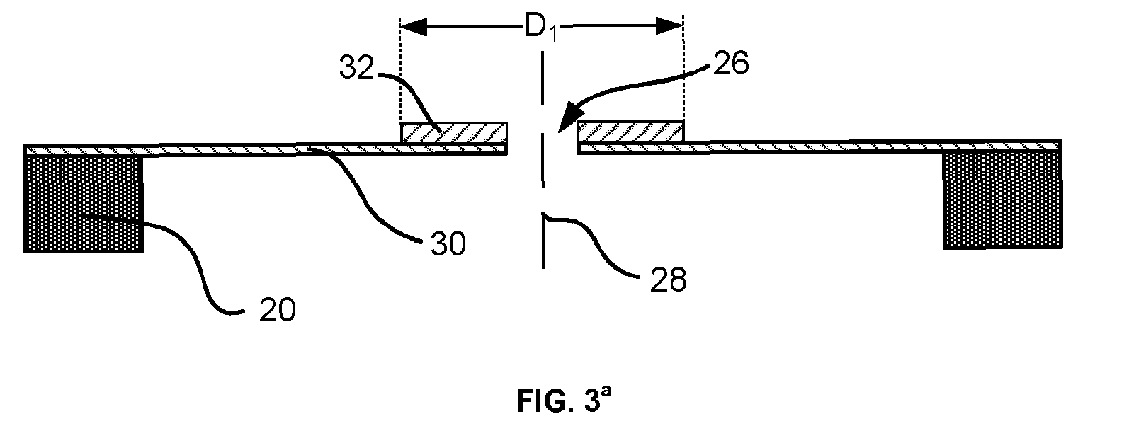
- FIG. 3 a schematically shows a first embodiment of a phase plate according to the invention.
- the phase plate shows a similar holder structure 20 as the prior art phase plate.
- a thin film 30 is mounted on the holder, the thin layer having little effect on the beam.
- an extra layer 32 is added to the thin layer, thus forming a first thin film with added thickness, whereby the part of the phase plate inside D 1 resembles the prior art phase plate, showing a thin film that causes a phase shift of - ⁇ /2, but between D 1 and the inner perimeter of the holder the film is much thinner and the phase shift much smaller than in prior art phase plates.
- Figure 3 b shows the CTF of said phase plate.
- the CTF of this phase plate is given by curve 300. It shows a first region at low spatial frequencies where the CTF is modified from a sine-like behavior to a cosine-like behavior, similar to curve 202 shown in figure 2 b . Following this region is a second region where it equals the CTF of a conventional microscope without phase plate, similar to curve 200 shown in figure 2 b . the two regions are stitched together at point 302, corresponding with a diameter D 1 of the film shown in figure 3 a , chosen such that the two regions show continuity. It is noted that it is possible to have continuity in
- Figure 4 a shows another embodiment of the phase plate according to the invention, in which another thin film ring surrounds the further thin film.
- This embodiment shows a phase plate comprising a further thin film formed as a first annulus 32 as described in the first embodiment, augmented with another annulus 34 surrounding the first annulus.
- the annuli 32 and 34 may have the same thickness, or different thicknesses (as shown).
- the result of this embodiment is that for a first range of spatial frequencies, corresponding with all electrons falling on the phase plate within diameter D 1 (but outside of the central hole) a first phase shift ⁇ 1 is achieved, for a second range of spatial frequencies corresponding with electrons falling on the phase plate between diameters D 1 and D 2 , a phase shift ⁇ 2 ⁇ 0, and a third range of spatial frequencies corresponding with electrons falling on the phase plate outside diameter D 2 , a phase shift ⁇ 3 .
- the CTF can be tuned for optimal contrast for a large range of spatial frequencies.
- annulus 34 shown is separated from the annulus 32, but the annuli 32 and 34 may also touch each other.
- phase plate comprising a number of annuli, thus showing resemblance with a zone plate as used in e.g. x-ray optics.
- modulation of the thickness of the annulus or annuli in a discrete or non-discrete fashion is possible.
- the CTF is also a function of the defocus, too many annuli or thickness modulation over a too large diameter may become impractical.
- Figure 4 b schematically shows the CTF of the phase plate shown in figure 4 a .
- Figure 5 shows a third embodiment of the phase plate according to the invention.
- the scattering of the further thin film is further diminished by forming the film as a number of spokes 50.
- the first thin film is now only partly surrounded by the further thin film, but most of the first thin film is surrounded by empty spaces 52. Electrons passing through these empty spaces are not scattered, and only part of the electrons impinging on the spokes are scattered.
- the phase difference of the electrons passing through the empty space and the spokes is small, and therefore the CTF of electrons falling on the spokes and those passing between the spokes is minimal. Therefore the image reconstructed by the interference of electrons in the image plane (at the detector or fluorescent screen) will be isotropic: it does not or hardly show an angular dependency in CTF caused by the phase plate.
- the scattering of electrons by the thin film does not lead to a different CTF, but in a decrease in signal-to-noise. This implies that more signal (impinging electrons) should be used to obtain an image with the same signal-to-noise. As known to the skilled artisan this may lead to damage of the sample, and thus to a lower quality of the images.
Landscapes
- Chemical & Material Sciences (AREA)
- Analytical Chemistry (AREA)
- Analysing Materials By The Use Of Radiation (AREA)
Abstract
Description
- The invention relates to a phase plate for an electron microscope, the microscope generating a beam of electrons, said beam of electrons passing through a sample, the beam of electrons after passing through the sample divided in an undiffracted beam and a diffracted beam, the sample imaged in an image plane where the undiffracted and the diffracted beams interfere to form an image, the phase plate placed in a plane where the undiffracted and the diffracted beam are focused, the phase plate comprising:
- A central area, said central area in working causing a first phase shift,
- A first thin film surrounding and bordering the central area, said first thin film in working causing a second phase shift differing from the first phase shift,
- A holder structure surrounding the first thin film for holding the phase plate,
- Such a phase plate is known from "Phase Contrast Enhancement with Phase Plates in Biological Electron Microscopy", K. Nagayama et al., Microscopy Today, Vol. 18 No. 4, July 2010, pages 10-13, further referred to as Nagayama [-1-], and is also known as a Zernike phase plate.
- In a Transmission Electron Microscope (TEM) a sample is imaged by passing a beam of energetic electrons with a selectable energy of, for example, between 40 keV and 400 keV, through the sample. For so-called weak-phase samples, such as biological samples, most electrons pass through the sample while some electrons are elastically or inelastically scattered, the elastically scattered electrons forming diffracted beams. The image is formed by interference of the elastically scattered and unscattered electrons (diffracted and undiffracted beams).
- A problem arises in that the Contrast Transfer Function (CTF) for low spatial frequencies in the image is zero or close to zero, resulting in low visibility of large objects/structures. This is caused by the fact that a camera or fluorescent screen at the image plane is sensitive to intensity variations, but not to phase variations of the impinging electron beam.
- A solution to this is the use of a phase plate, the phase plate introducing a phase difference between the diffracted beams and the undiffracted beam. There are two main types of phase plates: the so-called Zernike phase plate leaves the undiffracted beam unchanged, and causes a phase shift of the diffracted beams, while the so-called Boersch phase plate shifts the undiffracted beam while leaving the diffracted beams unchanged.
- The introduction of the phase difference by the phase plate changes the sine-like behavior of the CTF to a cosine-like behavior, and thus a maximum contrast for low spatial frequencies.
The invention described here relates to a Zernike phase plate as described by Nagayama [-1-], more specifically in itsfigure 5 . The phase plate is positioned in the diffraction plane of the objective lens, also known as the back-focal plane of this lens. In this plane the parallel beam impinging on the sample, and the parallel diffracted beams originating from the sample, are focused into spots. The central spot in this plane is passed through a central through-hole in the phase plate, and thus experiences no phase shift. Electrons passing outside the hole pass through a foil and experience a phase shift ϕ of preferable -π/2. The interference of the undiffracted and the diffracted beams now results in intensity modulation instead of phase modulation. - It is noted that the phase plate as described is mounted in the diffraction plane of the TEM, but that the phase plate can be mounted in any plane downstream of the diffraction plane that is an image plane thereof.
- It is further noted that the phase plate can be a coated phase plate as shown in Nagayama [-1-],
figure 5 , but that coating is not essential: as long as the electrons pass through sufficient material to experience a phase shift with respect to the electrons passing through the central area or through-hole, phase modulation is translated in intensity modulation. - It is also noted that, although a phase shift ϕ of -π/2 is preferred, for other phase shifts the phase modulation is at least in part translated in an intensity modulation.
- A problem with the known phase plate is that part of the electrons passing through the foil are scattered by the foil and do not contribute to the image formation in the image plane of the sample. This is mentioned in e.g. "Optimizing phase contrast in transmission electron microscopy with an electrostatic (Boersch) phase plate", E. Majorovits et al., Ultramicroscopy Vol. 107 (2007), pages 213-226, further referred to as Majorowits [-2-]. At page 215, left column, it mentions as an advantage of the Boersch type phase plate over the Zernike type phase plate: "The advantage of the Boersch phase plate is obvious: no further electron scattering is introduced into the beam path, which avoids possible contamination problems and additional inelastic or plural scattering. High-resolution information is not affected and is transferred in the phase contrast image at its full signal strength."
- Another problem is that, although at another spatial frequency, the CTF shows zeros, and thus spatial frequency bands with low contrast, resulting in low visibility of objects/structures with corresponding dimensions.
- The invention aims to provide at least a partial solution for one or both of these problems.
- To that end a phase plate according to the invention is characterized in that between the first thin film and the holder structure at least one further thin film is present, said further thin film in working causing a further phase shift differing from the second phase shift, the difference between first phase shift and further phase shift for a further range of spatial frequencies causing an improvement of the contrast in the image compared to the situation where the further phase shift would equal the second phase shift.
- The invention is based on the insight that for a first part of the CTF, corresponding to low spatial frequencies, it is beneficial to introduce a phase shift of approximately -π/2, thus changing the CTF from a sine-like behavior to a cosine-like behavior, but when for higher spatial frequencies the resulting absolute value of the CTF, |CTF|, is less than the |CTF| achieved without phase plate, it would have been better to do without this phase shift.
- It is noted that the CTF can be written as

where k is the spatial frequency, A(k) is the aperture function, E(k) the attenuation of the wave for higher spatial frequencies k, also called envelope function, X(k) a function of the aberrations of the electron optical system and ϕ the phase shift introduced by a phase plate (if present).
The value of A(k) and E(k) are always less than unity, and thus the maximum attainable is a function of the spatial frequency k and less than one. As the maximum value of sin(X(k)+ ϕ) for a proper ϕ equals 1, the maximum attainable contrast transfer function is denoted by
- The improved phase plate described here preferably comprises a first thin film preferably formed as a first annulus causing a second phase shift and a further thin film preferably formed as an annulus surrounding and bordering the first annular area causing a further phase shift different from the second phase shift. This enables tuning the CTF for different spatial frequencies with different phase shifts.
- Preferably the CTF caused by the outer edge of the first thin film equals the CTF of the inner edge of the further thin film, thereby joining the CTF for both films without discontinuity.
- In a preferred embodiment the central area of the phase plate is a through-hole.
- Although strictly only a phase difference between the central, undiffracted beam and the diffracted beam is required, preferably the central beam passes through a through-hole in the film, thereby avoiding electrons from the intense central beam to impinge on the foil and cause problems like heating, contamination, charging and the like.
- Preferably the first phase shift caused by the first thin film is approximately -π/2, although small deviations do not change the CTF for low spatial frequencies much: a deviation of, for example, π/10, resulting in a phase shift of (-π/2 ± π/10) gives an almost identical contrast for low spatial frequencies.
- Preferably the first thin film changes the |CTF| such, that |CTF| ≥ 0.5 x CTFm for electrons impinging on this first thin film, whereas the |CTF| without the phase plate would be below 0.5 x CTFm.
Likewise the further thin film preferably causes a phase shift such that the |CTF| is kept above 0.5 x CTFm for electrons impinging on this further thin film, where the phase plate described by Nagayama [-1-] would give a |CTFm| below 0.5 x CTFm for said range of frequencies. More preferably the first and the further thin film should cause aphase shifts resulting in a |CTF| ≥ 0.7 x CTFm for electrons impinging on these thin films. - The skilled artisan will recognize that a graphene layer or a graphene double layer is preferred as further thin layer.
- Preferably the further thin film improves the |CTF| for the electrons impinging on said further thin film from a value of less than 0.5 x CTFm(k) to a value in excess of 0.5 x CTFm(k) for electrons impinging on this further thin film, at least at the position where first thin film and second thin film border, more specifically from a value of less than 0.7 x CTFm(k) to a value of at least 0.7 x CTFm.
- For electrons impinging further from the central beam (from the axis), the electrons fall on the thinner film, and hardly experience any phase shift or scattering. This is thus a situation that corresponds with the first maximum of the |CTF| in microscopes without a conventional phase plate. Therefore the phase plate according to the invention shows a first spatial frequency range where the sine-like function is phase shifted to a cosine-like function, and a further spatial frequency range where the CTF is (almost) identical to the CTF of a microscope without phase plate.
- The phase plate according to the invention thus has an improved |CTF| over a microscope equipped with a conventional phase plate and a microscope without a phase plate. Compared to a microscope with a conventional phase plate the scattering of electrons out of the beam by the phase plate is also less, resulting in more electrons contributing to the image.
- It is noted that more thin films, preferably in the form of concentric annuli, may be used. The phase shift of these annuli may differ from each other, either by using different materials or by using different thicknesses. In this way a phase plate resembling a Zone plate may be constructed, where correction of the CTF for numerous frequency intervals may be used.
- The invention is now elucidated using figures, where identical reference numerals indicate corresponding features.
To that end: -
Figure 1 schematically shows a TEM equipped with a phase plate -
Figure 2 a schematically shows a prior art phase plate, and -
Figure 2 b schematically shows the corresponding CTF, compared to the CTF of a conventional TEM without phase plate; -
Figure 3 a schematically shows a first embodiment of a phase plate according to the invention, and -
Figure 3 b schematically shows the corresponding CTF; -
Figure 4 a schematically shows a second embodiment of a phase plate according to the invention, and -
Figure 4 b schematically shows the corresponding CTF; -
Figure 5 schematically shows a third embodiment of a phase plate -
Figure 1 schematically shows a TEM 100 equipped with a phase plate. -
Figure 1 shows aparticle source 104 producing a beam of particles, such as electrons, along optical axis 102. The particles have a selectable energy of typically between 80 - 300 keV, although higher energies, e.g. 400 keV - 1 MeV, or lower energies, e.g. 50 keV, may be used. The beam of particles is manipulated bycondenser system 106 to form a parallel beam impinging on asample 108, the sample positioned with asample holder 110. The sample holder can position the sample with respect to the optical axis and may shift the sample in the plane perpendicular to the optical axis and tilt the sample with respect to said axis.Objective lens 112 forms a magnified image of the sample. The objective lens is followed by a magnifyingsystem 116, e.g. a doublet of lenses, forming an enlarged image of the back-focal plane 114 of the objective lens. Aphase plate 118 is placed in an enlarged image of the back-focal plane of the objective lens, this conjugated plane positioned between the magnifying system and aprojection system 122. The magnifyingsystem 122 thus forms an image of the back-focal plane with a variable magnification. The phase plate is positioned with amanipulator 120, allowing the phase plate to be centered round the optical axis. The projection system forms a magnified image of the sample on adetector 124, thereby revealing sample details of e.g. 0.1 nm. The detector may take the form of a fluorescent screen, or e.g. a CCD camera. In the case of e.g. a fluorescent screen the screen can be viewed via theglass window 126.
To align the optical components on the axis the TEM comprises a large number of deflectors, schematically shown as 128-1..128-7, although other deflectors on other places may be included. - It is noted that the phase plate may also be positioned in the back-focal plane itself.
-
Figure 2 a schematically shows a prior art phase plate, known from e.g. Nagayama [-1-].
It shows aholder structure 20 in the form of, for example, a standard platinum diaphragm with an aperture, as routinely used in electron microscopes. The outer diameter of such a standard platinum diaphragm is typically 3.05 mm, although other diameters are used. On this holder structure athin foil 22 of amorphous carbon is placed. As such foils are often contaminated with charging particles or such like (not shown), one of the last fabrication steps involves covering thelayer 24 with a carbon coating. The carbon coating is typically made by vacuum evaporation, resulting in an additional amorphous carbon layer.
The centre of the foil shows a through-hole 26 for passing the undiffracted beam. This hole has a diameter sufficient to pass the undiffracted beam, but preferably not much more, as then slightly scattered electrons, corresponding with electrons scattered by large structures (low spatial frequencies) do not pass through the foil to get the required phase shift but instead through the central hole. Typically the through-hole shows a diameter of less than 1 µm, formed in the foil using a focused ion beam.
The phase plate preferable shows rotational symmetry aroundaxis 28. - The electrons passing through the carbon exhibit a phase shift as a result of the internal potential of the carbon. The relation of the thickness T of the amorphous carbon film(s) and the phase shift ϕ caused by passing through said film is described by Motoki [-3-]:


h is Plank's constant and Ve is the velocity of an incident electron. The averaged inner potential of amorphous carbon is 7.8 V and σ is 0.00892 (V · nm)-1 for 300 keV electrons.
With these values, the thickness T of a carbon phase plate is calculated to be 31 nm for a phase shift ϕ = -π/2 (for 300 keV electrons).
It is noted that this prior art phase plate uses a round diaphragm as holder structure (support structure), but that also silicon structures (with a round or square inner or outer perimeter) are known to be used. Such a silicon phase plate can be made using lithographic techniques, optionally combined with ion beam milling for forming the central through-hole in the thin film. It is further noted that traditionally carbon is used for the thin film of prior art phase plates. However, other materials such as silicon may be used.
An overview of inner potentials and foil thicknesses for carbon, silicon and silicon nitride for different electron beam energies is given in table 1.Tabel 1: calculated film thickness to achieve ϕ = -π/2 for a Zernike phase plate as a function of beam energy for different materials. Film thickness [nm] for ϕ = -π/2 Material Vav [V] 100 keV 200 keV 300 keV C 7.8 21.8 27.6 30.9 Si 12.6 13.5 17.1 19.1 SiN 12.6 13.5 17.1 19.1 -
Figure 2 b schematically shows the CTF of the prior art Zernike phase plate shown infigure 2 a, compared to the CTF obtained without phase plate. - In
figure 2 b the CTF is shown in the so-called Scherzer defocus. The aperture function as mentioned in formula -1- is represented bycurve 204, the envelope function E(k) is represented bycurve 206. Theproduct 208 of these two, the CTFm(k), is typically almost identical to the envelop function. Without phase shift (without phase plate), so with ϕ = 0, the resultant CTF is represented by the sine-like function 200. With a phase shift of -π/2 the CTF changes to the cosine-like function 202. The result is that the introduction of phase shift enables imaging large structures (low spatial frequencies). However, zero crossings will occur at higher spatial frequencies in both cases, although the zero crossings occur at different spatial frequencies. - A disadvantage of this type of phase plate is that electrons scattered by the sample must pass through the carbon film, said carbon film again scattering part of the electrons from the beam, resulting in the loss of information, and thus an increase of the signal-to-noise ratio in the image. Also, the introduction of the phase plate introduces zeros where the absolute value of the CTF without phase plate has a maximum, and at these spatial frequencies thus decreases the visibility of the corresponding structures compared to a situation where no phase plate would have been used.
- It is noted that typically approximately 20% of the electrons impinging on
foil 22 are scattered from the beam, and thus lost for imaging. -
Figure 3 a schematically shows a first embodiment of a phase plate according to the invention.
The phase plate shows asimilar holder structure 20 as the prior art phase plate. Athin film 30 is mounted on the holder, the thin layer having little effect on the beam. Inside diameter D1 anextra layer 32 is added to the thin layer, thus forming a first thin film with added thickness, whereby the part of the phase plate inside D1 resembles the prior art phase plate, showing a thin film that causes a phase shift of -π/2, but between D1 and the inner perimeter of the holder the film is much thinner and the phase shift much smaller than in prior art phase plates. The result is that electrons passing through thefilm 32 are shifted over -π/2, but electrons passing though the phase plate outside D1 are shifted much less, for example over - π/10 (for 300 keV corresponding to a carbon layer of approximately 6 nm). Therefore the CTF for these electrons resembles the CTF of a conventional microscope without phase plate, and as the film is thinner than in prior art phase plates, also the scattering by said film is less. -
Figure 3 b shows the CTF of said phase plate. The CTF of this phase plate is given bycurve 300. It shows a first region at low spatial frequencies where the CTF is modified from a sine-like behavior to a cosine-like behavior, similar tocurve 202 shown infigure 2 b. Following this region is a second region where it equals the CTF of a conventional microscope without phase plate, similar tocurve 200 shown infigure 2 b. the two regions are stitched together atpoint 302, corresponding with a diameter D1 of the film shown infigure 3 a, chosen such that the two regions show continuity.
It is noted that it is possible to have continuity in |CTF| without having continuity in CTF: this implies that the contrast changes from black/white to white/black instantaneously. This is in most cases an unwanted situation.
It is further noted that for optimum performance (read: |CTF|) it may be attractive to chose another defocus than Scherzer defocus: the intent is to have as large a region as possible where the CTF is far removed from zero. -
Figure 4 a shows another embodiment of the phase plate according to the invention, in which another thin film ring surrounds the further thin film.
This embodiment shows a phase plate comprising a further thin film formed as afirst annulus 32 as described in the first embodiment, augmented with anotherannulus 34 surrounding the first annulus. Theannuli - It is noted that the
annulus 34 shown is separated from theannulus 32, but theannuli - As the person skilled in the art will recognize, it is possible to form a phase plate comprising a number of annuli, thus showing resemblance with a zone plate as used in e.g. x-ray optics. Also modulation of the thickness of the annulus or annuli in a discrete or non-discrete fashion is possible. However, as the CTF is also a function of the defocus, too many annuli or thickness modulation over a too large diameter may become impractical.
-
Figure 4 b schematically shows the CTF of the phase plate shown infigure 4 a. - It shows a first region at low frequencies, joined to a second region between the
points -
Figure 5 shows a third embodiment of the phase plate according to the invention. In this embodiment the scattering of the further thin film is further diminished by forming the film as a number ofspokes 50. The first thin film is now only partly surrounded by the further thin film, but most of the first thin film is surrounded byempty spaces 52. Electrons passing through these empty spaces are not scattered, and only part of the electrons impinging on the spokes are scattered. The phase difference of the electrons passing through the empty space and the spokes is small, and therefore the CTF of electrons falling on the spokes and those passing between the spokes is minimal. Therefore the image reconstructed by the interference of electrons in the image plane (at the detector or fluorescent screen) will be isotropic: it does not or hardly show an angular dependency in CTF caused by the phase plate. - It is noted that the scattering of electrons by the thin film does not lead to a different CTF, but in a decrease in signal-to-noise. This implies that more signal (impinging electrons) should be used to obtain an image with the same signal-to-noise. As known to the skilled artisan this may lead to damage of the sample, and thus to a lower quality of the images.
-
- [-1-] "Phase Contrast Enhancement with Phase Plates in Biological Electron Microscopy", K. Nagayama et al., Microscopy Today, Vol. 18 No. 4, July 2010, pages 10-13.
- [-2-] "Optimizing phase contrast in transmission electron microscopy with an electrostatic (Boersch) phase plate", E. Majorovits et al., Ultramicroscopy Vol. 107 (2007), pages 213-226.
- [-3-] "200 kV TEM with a Zernike phase plate", S. Motoki et al., Microsc. Microanal. 11 (Suppl 2), 2005, pages 708-709.
Claims (11)
- Phase plate (118) for an electron microscope (100), the microscope generating a beam of electrons, said beam of electrons passing through a sample (108), the beam of electrons after passing through the sample divided in an undiffracted beam and a diffracted beam, the sample imaged in an image plane where the undiffracted and the diffracted beams interfere to form an image, the phase plate placed in a plane where the undiffracted and the diffracted beam are focused, the phase plate comprising:• A central area (26), said central area in working causing a first phase shift,• A first thin film (32) surrounding and bordering the central area, said first thin film in working causing a second phase shift differing from the first phase shift,• A holder structure (20) surrounding the first thin film for holding the phase plate,
the difference between first phase shift and second phase shift causing an improvement of the contrast in the image for a range of spatial frequencies,
characterized in that• Between the first thin film (32) and the holder structure (20) at least one further thin film (30) is present, said further thin film in working causing a further phase shift differing from the second phase shift, the difference between first phase shift and further phase shift for a further range of spatial frequencies causing an improvement of the contrast in the image compared to the situation where the further phase shift would equal the second phase shift. - The phase plate of claim 1 in which the central area (26) is a through-hole, and the first phase shift thus equals zero.
- The phase plate of claim 1 or claim 2 in which the first thin film (32) and the further thin film (30) are formed as concentric annuli, the annulus forming the further thin film surrounding and bordering the annulus forming the first thin film, the centre of the annuli coinciding with the middle of the central area.
- The phase plate of any of the preceding claims in which the first thin film (32) causes a phase shift such, that the absolute value of the Contrast Transfer Function (300), |CTF| of the corresponding frequency range is changed from a value of at most 0.5 of the maximum attainable CTF (208) to a value of at least 0.5 of the maximum attainable CTF, more specifically from a value of less than 0.7 of the maximum attainable CTF to a value of at least 0.7 of the maximum attainable CTF.
- The phase plate of any of the preceding claims in which the further thin film (30) causes a phase shift such, that in said further range of spatial frequencies |CTF| of the corresponding frequency range is changed from a value of at most 0.5 of the maximum attainable CTF to a value of at least 0.5 of the maximum attainable CTF, more specifically from a value of less than 0.7 of the maximum attainable CTF to a value of at least 0.7 of the maximum attainable CTF.
- The phase plate of any of the preceding claims in which the further thin layer (30) is a graphene layer or a graphene double-layer.
- The phase plate of claim 1 or claim 2 in which the thickness of at least one of the thin films the thin films (32, 30) is modulated as a function of the distance from the center in such a way that the resultant absolute value of the |CTF| is for the corresponding frequency range above 0.5 of the maximum attainable CTF, more specifically more than 0.7 of the maximum attainable CTF, most specifically more than 0.9 of the maximum attainable CTF.
- The phase plate of claim 7 in which the CTF (300) does not change sign for the frequency (302) corresponding to the outer edge of the first thin film (32) and the inner edge of the further thin film (30).
- The phase plate of any of the preceding claims in which the first thin (32) film and the further film (30) show a difference in thickness, as a result of which the phase shift caused by the first thin film and the further thin film differ.
- The phase plate of any of claims 1-8 in which the first thin film (32) and the further thin film (30) show materials with different averaged internal potentials, as a result of which the phase shift caused by the first thin film and the further thin film differ.
- The phase plate of any claims 1-6 in which the further thin film shows openings (52), the first thin layer (32) connected to the holder structure by spokes (50) dividing the openings.
Priority Applications (5)
| Application Number | Priority Date | Filing Date | Title |
|---|---|---|---|
| EP20120168997 EP2667399A1 (en) | 2012-05-23 | 2012-05-23 | Improved phase plate for a TEM |
| JP2013102688A JP6027942B2 (en) | 2012-05-23 | 2013-05-15 | Phase plate for TEM |
| US13/896,103 US8772716B2 (en) | 2012-05-23 | 2013-05-16 | Phase plate for a TEM |
| CN201310194422.2A CN103560067B (en) | 2012-05-23 | 2013-05-23 | Improvement phase-plate for TEM |
| US14/271,828 US9006652B2 (en) | 2012-05-23 | 2014-05-07 | Phase shift method for a TEM |
Applications Claiming Priority (1)
| Application Number | Priority Date | Filing Date | Title |
|---|---|---|---|
| EP20120168997 EP2667399A1 (en) | 2012-05-23 | 2012-05-23 | Improved phase plate for a TEM |
Publications (1)
| Publication Number | Publication Date |
|---|---|
| EP2667399A1 true EP2667399A1 (en) | 2013-11-27 |
Family
ID=46149231
Family Applications (1)
| Application Number | Title | Priority Date | Filing Date |
|---|---|---|---|
| EP20120168997 Withdrawn EP2667399A1 (en) | 2012-05-23 | 2012-05-23 | Improved phase plate for a TEM |
Country Status (4)
| Country | Link |
|---|---|
| US (2) | US8772716B2 (en) |
| EP (1) | EP2667399A1 (en) |
| JP (1) | JP6027942B2 (en) |
| CN (1) | CN103560067B (en) |
Cited By (1)
| Publication number | Priority date | Publication date | Assignee | Title |
|---|---|---|---|---|
| EP3067912A1 (en) * | 2015-03-12 | 2016-09-14 | JEOL Ltd. | Phase plate, method of fabricating same, and electron microscope |
Families Citing this family (15)
| Publication number | Priority date | Publication date | Assignee | Title |
|---|---|---|---|---|
| EP2667399A1 (en) * | 2012-05-23 | 2013-11-27 | FEI Company | Improved phase plate for a TEM |
| EP2690648B1 (en) * | 2012-07-26 | 2014-10-15 | Fei Company | Method of preparing and imaging a lamella in a particle-optical apparatus |
| TWI544513B (en) * | 2012-12-18 | 2016-08-01 | 中央研究院 | On-chip thin film zernike phase plate capable of releasing charges and method for observing organic materials by using the same |
| JP6286270B2 (en) | 2013-04-25 | 2018-02-28 | エフ イー アイ カンパニFei Company | Method using a phase plate in a transmission electron microscope |
| DE102013019297A1 (en) | 2013-11-19 | 2015-05-21 | Fei Company | Phase plate for a transmission electron microscope |
| EP2881970A1 (en) | 2013-12-04 | 2015-06-10 | Fei Company | Method of producing a freestanding thin film of nano-crystalline carbon |
| EP3097577A4 (en) * | 2014-01-21 | 2017-09-20 | Ramot at Tel-Aviv University Ltd. | Method and device for manipulating particle beam |
| JP2016110767A (en) * | 2014-12-04 | 2016-06-20 | 日本電子株式会社 | Charged particle beam device and image achieving method |
| US10109453B2 (en) * | 2015-03-18 | 2018-10-23 | Battelle Memorial Institute | Electron beam masks for compressive sensors |
| US10170274B2 (en) | 2015-03-18 | 2019-01-01 | Battelle Memorial Institute | TEM phase contrast imaging with image plane phase grating |
| US10580614B2 (en) | 2016-04-29 | 2020-03-03 | Battelle Memorial Institute | Compressive scanning spectroscopy |
| JP6449526B2 (en) * | 2016-08-22 | 2019-01-09 | 株式会社日立ハイテクノロジーズ | Electron microscope and observation method |
| US10295677B2 (en) | 2017-05-08 | 2019-05-21 | Battelle Memorial Institute | Systems and methods for data storage and retrieval |
| JP7051591B2 (en) * | 2018-06-05 | 2022-04-11 | 株式会社日立製作所 | Transmission electron microscope |
| WO2020243268A1 (en) | 2019-05-28 | 2020-12-03 | The Board Of Trustees Of The Leland Stanford Junior University | Optically-addressed phase modulator for electron beams |
Citations (1)
| Publication number | Priority date | Publication date | Assignee | Title |
|---|---|---|---|---|
| EP2159818A1 (en) * | 2008-08-27 | 2010-03-03 | Max-Planck-Gesellschaft zur Förderung der Wissenschaften e.V. | Phase plate, in particular for an electron microscope |
Family Cites Families (14)
| Publication number | Priority date | Publication date | Assignee | Title |
|---|---|---|---|---|
| JP3773389B2 (en) * | 2000-03-27 | 2006-05-10 | 日本電子株式会社 | Thin film phase plate for phase contrast electron microscope, phase contrast electron microscope and phase plate antistatic method |
| JP4328044B2 (en) * | 2001-09-25 | 2009-09-09 | 日本電子株式会社 | Differential contrast electron microscope and data processing method of electron microscope image |
| DE10200645A1 (en) * | 2002-01-10 | 2003-07-24 | Leo Elektronenmikroskopie Gmbh | Electron microscope with circular illumination aperture |
| US7737412B2 (en) * | 2004-07-12 | 2010-06-15 | The Regents Of The University Of California | Electron microscope phase enhancement |
| JP4625317B2 (en) * | 2004-12-03 | 2011-02-02 | ナガヤマ アイピー ホールディングス リミテッド ライアビリティ カンパニー | Phase plate for phase contrast electron microscope, method for producing the same, and phase contrast electron microscope |
| DE102005040267B4 (en) * | 2005-08-24 | 2007-12-27 | Universität Karlsruhe | Method for producing a multilayer electrostatic lens arrangement, in particular a phase plate and such a phase plate |
| EP2091062A1 (en) | 2008-02-13 | 2009-08-19 | FEI Company | TEM with aberration corrector and phase plate |
| EP2131385A1 (en) * | 2008-06-05 | 2009-12-09 | FEI Company | Hybrid phase plate |
| JP4896106B2 (en) * | 2008-09-30 | 2012-03-14 | 株式会社日立ハイテクノロジーズ | electronic microscope |
| EP2400522A1 (en) | 2010-06-24 | 2011-12-28 | Fei Company | Blocking member for use in the diffraction plane of a TEM |
| CN102971824B (en) | 2010-07-14 | 2016-01-13 | Fei公司 | For the improvement contrast of scanning confocal electron microscope |
| EP2485239A1 (en) * | 2011-02-07 | 2012-08-08 | FEI Company | Method for centering an optical element in a TEM comprising a contrast enhancing element |
| EP2667399A1 (en) * | 2012-05-23 | 2013-11-27 | FEI Company | Improved phase plate for a TEM |
| EP2704178B1 (en) | 2012-08-30 | 2014-08-20 | Fei Company | Imaging a sample in a TEM equipped with a phase plate |
-
2012
- 2012-05-23 EP EP20120168997 patent/EP2667399A1/en not_active Withdrawn
-
2013
- 2013-05-15 JP JP2013102688A patent/JP6027942B2/en active Active
- 2013-05-16 US US13/896,103 patent/US8772716B2/en active Active
- 2013-05-23 CN CN201310194422.2A patent/CN103560067B/en active Active
-
2014
- 2014-05-07 US US14/271,828 patent/US9006652B2/en active Active
Patent Citations (1)
| Publication number | Priority date | Publication date | Assignee | Title |
|---|---|---|---|---|
| EP2159818A1 (en) * | 2008-08-27 | 2010-03-03 | Max-Planck-Gesellschaft zur Förderung der Wissenschaften e.V. | Phase plate, in particular for an electron microscope |
Non-Patent Citations (7)
| Title |
|---|
| DANEV R ET AL: "Practical factors affecting the performance of a thin-film phase plate for transmission electron microscopy", ULTRAMICROSCOPY, ELSEVIER, AMSTERDAM, NL, vol. 109, no. 4, 1 March 2009 (2009-03-01), pages 312 - 325, XP025981122, ISSN: 0304-3991, [retrieved on 20081211], DOI: 10.1016/J.ULTRAMIC.2008.12.006 * |
| E. MAJOROVITS ET AL.: "Optimizing phase contrast in transmission electron microscopy with an electrostatic (Boersch) phase plate", ULTRAMICROSCOPY, vol. 107, 2007, pages 213 - 226, XP002418323, DOI: doi:10.1016/j.ultramic.2006.07.006 |
| K. NAGAYAMA ET AL.: "Phase Contrast Enhancement with Phase Plates in Biological Electron Microscopy", MICROSCOPY TODAY, vol. 18, no. 4, July 2010 (2010-07-01), pages 10 - 13, XP055049018, DOI: doi:10.1017/S1551929510000465 |
| KUNIAKI NAGAYAMA: "Development of phase plates for electron microscopes and their biological application", EUROPEAN BIOPHYSICS JOURNAL, vol. 37, no. 4, 8 February 2008 (2008-02-08), pages 345 - 358, XP055027869, ISSN: 0175-7571, DOI: 10.1007/s00249-008-0264-5 * |
| LENTZEN M: "The tuning of a Zernike phase plate with defocus and variable spherical aberration and its use in HRTEM imaging", ULTRAMICROSCOPY, ELSEVIER, AMSTERDAM, NL, vol. 99, 1 January 2004 (2004-01-01), pages 211 - 220, XP007905965, ISSN: 0304-3991, DOI: 10.1016/J.ULTRAMIC.2003.12.007 * |
| MULLER K: "Phase plates for electron microscopes", OPTIK, WISSENSCHAFTLICHE VERLAG GMBH, DE, vol. 45, no. 1, 1 January 1976 (1976-01-01), pages 73 - 85, XP009134533, ISSN: 0030-4026 * |
| S. MOTOKI ET AL.: "200 kV TEM with a Zernike phase plate", MICROSC. MICROANAL., vol. 11, no. 2, 2005, pages 708 - 709 |
Cited By (1)
| Publication number | Priority date | Publication date | Assignee | Title |
|---|---|---|---|---|
| EP3067912A1 (en) * | 2015-03-12 | 2016-09-14 | JEOL Ltd. | Phase plate, method of fabricating same, and electron microscope |
Also Published As
| Publication number | Publication date |
|---|---|
| CN103560067B (en) | 2018-05-15 |
| US8772716B2 (en) | 2014-07-08 |
| JP2013247113A (en) | 2013-12-09 |
| US9006652B2 (en) | 2015-04-14 |
| CN103560067A (en) | 2014-02-05 |
| US20130313428A1 (en) | 2013-11-28 |
| US20140326878A1 (en) | 2014-11-06 |
| JP6027942B2 (en) | 2016-11-16 |
Similar Documents
| Publication | Publication Date | Title |
|---|---|---|
| US9006652B2 (en) | Phase shift method for a TEM | |
| CN103681187B (en) | To being equipped with the sample in the TEM of phase-plate to carry out imaging | |
| JP5388163B2 (en) | Phase-shifting element and particle beam apparatus having phase-shifting element | |
| US6191423B1 (en) | Correction device for correcting the spherical aberration in particle-optical apparatus | |
| EP2131384B1 (en) | Hybrid phase plate | |
| JP5965656B2 (en) | Method for centering an optical element in a TEM comprising an element for improving contrast | |
| JP2009193963A (en) | TEM with aberration corrector and phase plate | |
| JP3987276B2 (en) | Sample image forming method | |
| US7977633B2 (en) | Phase plate, in particular for an electron microscope | |
| JP5829842B2 (en) | Blocking member for use in the TEM diffraction plane | |
| US10497537B2 (en) | Method and device for manipulating particle beam | |
| JP3896150B2 (en) | Spherical aberration correction device for electron microscope | |
| JP2021161531A (en) | Electron microscope aberration correction lens and its manufacturing method, and manufacturing equipment | |
| Isakozawa et al. | Recent Development in Hitachi Transmission Electron Microscope |
Legal Events
| Date | Code | Title | Description |
|---|---|---|---|
| PUAI | Public reference made under article 153(3) epc to a published international application that has entered the european phase |
Free format text: ORIGINAL CODE: 0009012 |
|
| AK | Designated contracting states |
Kind code of ref document: A1 Designated state(s): AL AT BE BG CH CY CZ DE DK EE ES FI FR GB GR HR HU IE IS IT LI LT LU LV MC MK MT NL NO PL PT RO RS SE SI SK SM TR |
|
| AX | Request for extension of the european patent |
Extension state: BA ME |
|
| 17P | Request for examination filed |
Effective date: 20140513 |
|
| RBV | Designated contracting states (corrected) |
Designated state(s): AL AT BE BG CH CY CZ DE DK EE ES FI FR GB GR HR HU IE IS IT LI LT LU LV MC MK MT NL NO PL PT RO RS SE SI SK SM TR |
|
| RIC1 | Information provided on ipc code assigned before grant |
Ipc: H01J 37/26 20060101AFI20140528BHEP |
|
| 17Q | First examination report despatched |
Effective date: 20140613 |
|
| STAA | Information on the status of an ep patent application or granted ep patent |
Free format text: STATUS: THE APPLICATION IS DEEMED TO BE WITHDRAWN |
|
| 18D | Application deemed to be withdrawn |
Effective date: 20141028 |