EP2667246A1 - Portable display device and method of assembling the same - Google Patents
Portable display device and method of assembling the same Download PDFInfo
- Publication number
- EP2667246A1 EP2667246A1 EP13164066.6A EP13164066A EP2667246A1 EP 2667246 A1 EP2667246 A1 EP 2667246A1 EP 13164066 A EP13164066 A EP 13164066A EP 2667246 A1 EP2667246 A1 EP 2667246A1
- Authority
- EP
- European Patent Office
- Prior art keywords
- blocking member
- drive circuit
- display device
- region
- display panel
- Prior art date
- Legal status (The legal status is an assumption and is not a legal conclusion. Google has not performed a legal analysis and makes no representation as to the accuracy of the status listed.)
- Withdrawn
Links
Images




Classifications
-
- H—ELECTRICITY
- H04—ELECTRIC COMMUNICATION TECHNIQUE
- H04B—TRANSMISSION
- H04B1/00—Details of transmission systems, not covered by a single one of groups H04B3/00 - H04B13/00; Details of transmission systems not characterised by the medium used for transmission
- H04B1/38—Transceivers, i.e. devices in which transmitter and receiver form a structural unit and in which at least one part is used for functions of transmitting and receiving
-
- G—PHYSICS
- G02—OPTICS
- G02F—OPTICAL DEVICES OR ARRANGEMENTS FOR THE CONTROL OF LIGHT BY MODIFICATION OF THE OPTICAL PROPERTIES OF THE MEDIA OF THE ELEMENTS INVOLVED THEREIN; NON-LINEAR OPTICS; FREQUENCY-CHANGING OF LIGHT; OPTICAL LOGIC ELEMENTS; OPTICAL ANALOGUE/DIGITAL CONVERTERS
- G02F1/00—Devices or arrangements for the control of the intensity, colour, phase, polarisation or direction of light arriving from an independent light source, e.g. switching, gating or modulating; Non-linear optics
- G02F1/01—Devices or arrangements for the control of the intensity, colour, phase, polarisation or direction of light arriving from an independent light source, e.g. switching, gating or modulating; Non-linear optics for the control of the intensity, phase, polarisation or colour
- G02F1/13—Devices or arrangements for the control of the intensity, colour, phase, polarisation or direction of light arriving from an independent light source, e.g. switching, gating or modulating; Non-linear optics for the control of the intensity, phase, polarisation or colour based on liquid crystals, e.g. single liquid crystal display cells
- G02F1/133—Constructional arrangements; Operation of liquid crystal cells; Circuit arrangements
- G02F1/1333—Constructional arrangements; Manufacturing methods
-
- G—PHYSICS
- G02—OPTICS
- G02F—OPTICAL DEVICES OR ARRANGEMENTS FOR THE CONTROL OF LIGHT BY MODIFICATION OF THE OPTICAL PROPERTIES OF THE MEDIA OF THE ELEMENTS INVOLVED THEREIN; NON-LINEAR OPTICS; FREQUENCY-CHANGING OF LIGHT; OPTICAL LOGIC ELEMENTS; OPTICAL ANALOGUE/DIGITAL CONVERTERS
- G02F1/00—Devices or arrangements for the control of the intensity, colour, phase, polarisation or direction of light arriving from an independent light source, e.g. switching, gating or modulating; Non-linear optics
- G02F1/01—Devices or arrangements for the control of the intensity, colour, phase, polarisation or direction of light arriving from an independent light source, e.g. switching, gating or modulating; Non-linear optics for the control of the intensity, phase, polarisation or colour
- G02F1/13—Devices or arrangements for the control of the intensity, colour, phase, polarisation or direction of light arriving from an independent light source, e.g. switching, gating or modulating; Non-linear optics for the control of the intensity, phase, polarisation or colour based on liquid crystals, e.g. single liquid crystal display cells
- G02F1/133—Constructional arrangements; Operation of liquid crystal cells; Circuit arrangements
- G02F1/1333—Constructional arrangements; Manufacturing methods
- G02F1/1345—Conductors connecting electrodes to cell terminals
- G02F1/13452—Conductors connecting driver circuitry and terminals of panels
-
- G—PHYSICS
- G09—EDUCATION; CRYPTOGRAPHY; DISPLAY; ADVERTISING; SEALS
- G09F—DISPLAYING; ADVERTISING; SIGNS; LABELS OR NAME-PLATES; SEALS
- G09F9/00—Indicating arrangements for variable information in which the information is built-up on a support by selection or combination of individual elements
-
- H—ELECTRICITY
- H05—ELECTRIC TECHNIQUES NOT OTHERWISE PROVIDED FOR
- H05K—PRINTED CIRCUITS; CASINGS OR CONSTRUCTIONAL DETAILS OF ELECTRIC APPARATUS; MANUFACTURE OF ASSEMBLAGES OF ELECTRICAL COMPONENTS
- H05K13/00—Apparatus or processes specially adapted for manufacturing or adjusting assemblages of electric components
- H05K13/04—Mounting of components, e.g. of leadless components
- H05K13/046—Surface mounting
- H05K13/0469—Surface mounting by applying a glue or viscous material
-
- H—ELECTRICITY
- H05—ELECTRIC TECHNIQUES NOT OTHERWISE PROVIDED FOR
- H05K—PRINTED CIRCUITS; CASINGS OR CONSTRUCTIONAL DETAILS OF ELECTRIC APPARATUS; MANUFACTURE OF ASSEMBLAGES OF ELECTRICAL COMPONENTS
- H05K7/00—Constructional details common to different types of electric apparatus
- H05K7/02—Arrangements of circuit components or wiring on supporting structure
-
- H—ELECTRICITY
- H10—SEMICONDUCTOR DEVICES; ELECTRIC SOLID-STATE DEVICES NOT OTHERWISE PROVIDED FOR
- H10K—ORGANIC ELECTRIC SOLID-STATE DEVICES
- H10K50/00—Organic light-emitting devices
- H10K50/80—Constructional details
- H10K50/84—Passivation; Containers; Encapsulations
- H10K50/841—Self-supporting sealing arrangements
-
- H—ELECTRICITY
- H10—SEMICONDUCTOR DEVICES; ELECTRIC SOLID-STATE DEVICES NOT OTHERWISE PROVIDED FOR
- H10K—ORGANIC ELECTRIC SOLID-STATE DEVICES
- H10K50/00—Organic light-emitting devices
- H10K50/80—Constructional details
- H10K50/84—Passivation; Containers; Encapsulations
- H10K50/842—Containers
- H10K50/8426—Peripheral sealing arrangements, e.g. adhesives, sealants
-
- H—ELECTRICITY
- H10—SEMICONDUCTOR DEVICES; ELECTRIC SOLID-STATE DEVICES NOT OTHERWISE PROVIDED FOR
- H10K—ORGANIC ELECTRIC SOLID-STATE DEVICES
- H10K59/00—Integrated devices, or assemblies of multiple devices, comprising at least one organic light-emitting element covered by group H10K50/00
- H10K59/80—Constructional details
- H10K59/87—Passivation; Containers; Encapsulations
- H10K59/871—Self-supporting sealing arrangements
- H10K59/872—Containers
-
- H—ELECTRICITY
- H10—SEMICONDUCTOR DEVICES; ELECTRIC SOLID-STATE DEVICES NOT OTHERWISE PROVIDED FOR
- H10K—ORGANIC ELECTRIC SOLID-STATE DEVICES
- H10K59/00—Integrated devices, or assemblies of multiple devices, comprising at least one organic light-emitting element covered by group H10K50/00
- H10K59/80—Constructional details
- H10K59/87—Passivation; Containers; Encapsulations
- H10K59/871—Self-supporting sealing arrangements
- H10K59/8722—Peripheral sealing arrangements, e.g. adhesives, sealants
-
- G—PHYSICS
- G02—OPTICS
- G02F—OPTICAL DEVICES OR ARRANGEMENTS FOR THE CONTROL OF LIGHT BY MODIFICATION OF THE OPTICAL PROPERTIES OF THE MEDIA OF THE ELEMENTS INVOLVED THEREIN; NON-LINEAR OPTICS; FREQUENCY-CHANGING OF LIGHT; OPTICAL LOGIC ELEMENTS; OPTICAL ANALOGUE/DIGITAL CONVERTERS
- G02F1/00—Devices or arrangements for the control of the intensity, colour, phase, polarisation or direction of light arriving from an independent light source, e.g. switching, gating or modulating; Non-linear optics
- G02F1/01—Devices or arrangements for the control of the intensity, colour, phase, polarisation or direction of light arriving from an independent light source, e.g. switching, gating or modulating; Non-linear optics for the control of the intensity, phase, polarisation or colour
- G02F1/13—Devices or arrangements for the control of the intensity, colour, phase, polarisation or direction of light arriving from an independent light source, e.g. switching, gating or modulating; Non-linear optics for the control of the intensity, phase, polarisation or colour based on liquid crystals, e.g. single liquid crystal display cells
- G02F1/133—Constructional arrangements; Operation of liquid crystal cells; Circuit arrangements
- G02F1/1333—Constructional arrangements; Manufacturing methods
- G02F1/133308—Support structures for LCD panels, e.g. frames or bezels
- G02F1/133331—Cover glasses
-
- G—PHYSICS
- G02—OPTICS
- G02F—OPTICAL DEVICES OR ARRANGEMENTS FOR THE CONTROL OF LIGHT BY MODIFICATION OF THE OPTICAL PROPERTIES OF THE MEDIA OF THE ELEMENTS INVOLVED THEREIN; NON-LINEAR OPTICS; FREQUENCY-CHANGING OF LIGHT; OPTICAL LOGIC ELEMENTS; OPTICAL ANALOGUE/DIGITAL CONVERTERS
- G02F2201/00—Constructional arrangements not provided for in groups G02F1/00 - G02F7/00
- G02F2201/50—Protective arrangements
- G02F2201/501—Blocking layers, e.g. against migration of ions
-
- G—PHYSICS
- G02—OPTICS
- G02F—OPTICAL DEVICES OR ARRANGEMENTS FOR THE CONTROL OF LIGHT BY MODIFICATION OF THE OPTICAL PROPERTIES OF THE MEDIA OF THE ELEMENTS INVOLVED THEREIN; NON-LINEAR OPTICS; FREQUENCY-CHANGING OF LIGHT; OPTICAL LOGIC ELEMENTS; OPTICAL ANALOGUE/DIGITAL CONVERTERS
- G02F2202/00—Materials and properties
- G02F2202/02—Materials and properties organic material
- G02F2202/022—Materials and properties organic material polymeric
- G02F2202/023—Materials and properties organic material polymeric curable
-
- G—PHYSICS
- G02—OPTICS
- G02F—OPTICAL DEVICES OR ARRANGEMENTS FOR THE CONTROL OF LIGHT BY MODIFICATION OF THE OPTICAL PROPERTIES OF THE MEDIA OF THE ELEMENTS INVOLVED THEREIN; NON-LINEAR OPTICS; FREQUENCY-CHANGING OF LIGHT; OPTICAL LOGIC ELEMENTS; OPTICAL ANALOGUE/DIGITAL CONVERTERS
- G02F2202/00—Materials and properties
- G02F2202/28—Adhesive materials or arrangements
-
- Y—GENERAL TAGGING OF NEW TECHNOLOGICAL DEVELOPMENTS; GENERAL TAGGING OF CROSS-SECTIONAL TECHNOLOGIES SPANNING OVER SEVERAL SECTIONS OF THE IPC; TECHNICAL SUBJECTS COVERED BY FORMER USPC CROSS-REFERENCE ART COLLECTIONS [XRACs] AND DIGESTS
- Y10—TECHNICAL SUBJECTS COVERED BY FORMER USPC
- Y10T—TECHNICAL SUBJECTS COVERED BY FORMER US CLASSIFICATION
- Y10T156/00—Adhesive bonding and miscellaneous chemical manufacture
- Y10T156/10—Methods of surface bonding and/or assembly therefor
Definitions
- the present invention generally relates to a portable display device and a method of assembling the same.
- a portable display device such as a cellular phone may include a display panel and a window.
- the window may be attached to the display panel using an attaching member such as a resin. Because the non-hardened resin may have the potential of flowing, a process for controlling flows of the resin coated on the display panel may be required. That is, controlling resin flows may prevent the resin from being spilled from the display panel.
- a barrier may be formed at four sides of the display panel to prevent the spill of the resin from the display panel.
- the barrier may include a resin different from the resin used for the attachment member.
- the resin used for the barrier may be expensive, a cost for manufacturing the portable display device may be increased.
- Example embodiments relate to a portable display device such as a cellular phone, and a method of assembling the portable display device.
- Example embodiments provide a portable display device that may be capable of controlling flows of a resin with a simple and cheap structure.
- Example embodiments provide a method of assembling the above-mentioned portable display device.
- a portable display device may include a display panel, a window, an attaching member and a blocking member.
- the display panel may have a drive circuit region and a display region.
- the window may be positioned facing to the display panel.
- the attaching member may be interposed between the display region of the display panel and the window to attach the display panel to the window.
- the blocking member may be arranged on a boundary line between the drive circuit region and the display region to prevent the attaching member from infiltrating into the drive circuit region.
- the drive circuit region may be located adjacent to only one side surface of the display panel.
- the blocking member may be wholly arranged on the boundary line.
- the blocking member may be parallel to the side surface of the display panel to which the drive circuit region may be located adjacent.
- the portable display device may further include a flexible printed circuit (FPC) arranged in the drive circuit region.
- the blocking member may be partially arranged on the boundary line to prevent the attaching member from infiltrating into the FPC.
- the blocking member may include a main blocking portion configured to cover a surface of the FPC exposed to the display region.
- the blocking member may further include an auxiliary blocking portion extended from the main blocking portion to cover both side surfaces of the FPC at both sides of the exposed surface.
- the display panel may further have a second drive circuit region.
- the portable display device may further include a second blocking member.
- the second blocking member may be arranged on a boundary line between the display region and the second drive circuit region to prevent the attaching member from infiltrating into the second drive circuit region.
- the portable display device may further include a second FPC arranged in the second drive circuit region.
- the second blocking member may be partially arranged on the boundary line to prevent the attaching member from infiltrating into the second FPC.
- the blocking member may include a transparent material.
- the blocking member may include a double-sided adhesive tape.
- the attaching member may include a resin.
- the blocking member may include a resin having a viscosity higher than that of the resin used for the attaching member.
- a portable display device may include a display panel, an FPC, a window, an attaching member and a blocking member.
- the FPC may be connected to the display panel.
- the window may be positioned facing to the display panel.
- the attaching member may be interposed between the display panel and the window to attach the display panel to the window.
- the blocking member may be configured to cover the FPC to prevent the attaching member from infiltrating into the FPC.
- the blocking member may include a main blocking portion configured to cover a first side surface of the FPC oriented toward a central portion of the display panel.
- the blocking member may further include an auxiliary blocking portion extended from the main blocking portion to cover both side surfaces of the FPC at both sides of the first side surface.
- a blocking member may be formed on a boundary line between a drive circuit region and a display region of a display panel.
- An attaching member may be coated on the display region of the display panel blocked from the drive circuit region by the blocking member.
- a window may be attached to the display panel using the attaching member.
- forming the blocking member may include attaching a double-sided adhesive tape to the boundary line.
- forming the blocking member may include coating a resin on the boundary line, and annealing the resin.
- coating the attaching member may include coating a resin.
- the method may further include annealing the attaching member.
- annealing the attaching member may include irradiating an ultraviolet light to the attaching member.
- a blocking member may cover a FPC connected to a display panel.
- An attaching member may be coated on the display panel.
- a window may be attached to the display panel using the attaching member.
- forming the blocking member may include attaching a double-sided adhesive tape to the FPC.
- the method may further include annealing the attaching member.
- annealing the attaching member may include irradiating an ultraviolet light to the attaching member.
- the blocking member may be arranged on only the boundary line between the display region and the drive circuit region of the display panel.
- flows of the attaching member may be readily controlled using the blocking member having a simple structure to prevent the infiltration of the attaching member into the drive circuit region.
- the portable display device may be assembled by a simple process and a low cost.
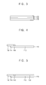
- FIG. 1 is a front view illustrating a portable display device in accordance with example embodiments
- FIG. 2 is a cross-sectional view taken along a line II-II' in FIG. 1
- FIG. 3 is a cross-sectional view taken along a line III-III' in FIG. 1 .
- a portable display device 100 of this example embodiment may include a display panel 110, a window 120, an attaching member 130 and a blocking member 140.
- the display panel 110 may have a rectangular cross-section. Thus, the display panel 110 may have four side surfaces. Further, the display panel 110 may have a display region 112 and a drive circuit region 114.
- the display panel 110 may include a liquid crystal display (LCD) panel, a plasma display panel, an organic light emitting display (OLED) panel, etc.
- the drive circuit region 114 may correspond to a single region having a rectangular shape that may be positioned adjacent to a lower surface of the display panel 110.
- the display region 112 may correspond to the rest region of the display panel 110 except for the drive circuit region 114. Shapes, sizes, positions, etc., of the drive circuit region 114 may vary in accordance with kinds of the portable display device 100.
- a flexible printed circuit (FPC) 150 may be arranged in the drive circuit region 114.
- the FPC 150 may apply electrical signals to the display region 112.
- the FPC 150 may be exposed to the display region 112.
- the window 120 may be arranged over the display panel 110.
- the window 120 may be attached to the display panel 110 using the attaching member 130.
- the attaching member 130 may be interposed between the window 120 and the display panel 110.
- the attaching member 130 may be located in only the display region 112. That is, the attaching member 130 may not be arranged in the drive circuit region 114.
- the attaching member 130 may include an insulating resin.
- the attaching member 130 may be formed by coating a flowable resin between the display panel 110 and the window 120, and by annealing the flowable resin.
- the flowable resin before annealing may flow from the display region 112 toward the drive circuit region 114.
- the blocking member 140 may be arranged on a boundary line between the display region 112 and the drive circuit region 114.
- the blocking member 140 may prevent the flowable region in the display region 112 from infiltrating into the drive circuit region 114.
- the blocking member 140 may prevent the insulating resin from being smeared on the flexible printed circuit (FPC) 150 in the drive circuit region 114.
- the blocking member 140 may not surround the four side surfaces of the display panel 110.
- the blocking member 140 may be arranged on only the boundary line between the display region 112 and the drive circuit region 114. Therefore, the blocking member 140 may have a long stripe shape substantially parallel with a lower side surface of the display panel 110. Further, the blocking member 140 may have a length substantially the same as that of the lower side surface of the display panel 110.
- the blocking member 140 may be extended along the whole boundary line between the display region 112 and the drive circuit region 114 to completely isolate the drive circuit region 114 from the display region 112. As a result, because the blocking member 140 may block flows of the attaching member 130 in the display region 112 toward the drive circuit region 114, the attaching member 130 may not infiltrate into the drive circuit region 114.
- the blocking member 140 may include a transparent material.
- the blocking member 140 may include a double-sided adhesive tape.
- the double-sided adhesive tape may be cheap. Further, the double-sided adhesive tape may be easily attached. Therefore, the portable display device 100 may be readily assembled by a simple process and a low cost. Furthermore, the double-sided adhesive tape may have a function as to attach the display panel 110 and the window 120 to each other.
- FIGS. 4 to 7 are cross-sectional views illustrating a method of assembling the portable display device in FIG. 1 .
- the blocking member 140 may be formed on the boundary line between the display region 112 and the drive circuit region 114 of the display panel 110.
- the blocking member 140 may include a transparent double-sided adhesive tape.
- the blocking member 140 may be easily formed by attaching the double-sided adhesive tape on the boundary line between the display region 112 and the drive circuit region 114.
- the attaching member 130 may be coated on the display region 112 of the display panel 110.
- the attaching member 130 may include an insulating resin. Because the insulating resin before annealing may have a flowable property, the resin may flow from the display region 112 into the drive circuit region 114. However, the blocking member 140 on the boundary line between the display region 112 and the drive circuit region 114 may block the resin, so that the resin may not infiltrate into the drive circuit region 114.
- the window 120 may be arranged on the attaching member 130. Because the attaching member 130 may not be annealed, the window 120 may not be attached to the display panel 110.
- the attaching member 130 may be annealed to firmly attach the window 120 and the display panel 130 to each other via the annealed attaching member 130, thereby completing the portable display device 100.
- the attaching member 130 may be annealed by irradiating an ultraviolet light to the resin.
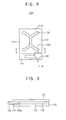
- FIG. 8 is a front view illustrating a portable display device in accordance with example embodiments
- FIG. 9 is a cross-sectional view taken along a line IX-IX' in FIG. 8
- FIG. 10 is a cross-sectional view taken along a line X-X' in FIG. 8 .
- a portable display device 100a of this example embodiment may include elements substantially the same as those of the portable display device 100 in FIG. 1 except for a blocking member 140a.
- the same reference numerals may refer to the same elements and any further illustrations with respect to the same element may be omitted herein for brevity.
- the blocking member 140a may block only the FPC 150.
- the blocking member 140a may be configured to cover a surface of the FPC 150 exposed to the display region 112 of the display panel 110.
- the blocking member 140a may make contact with the surface of the FPC 150.
- the blocking member 140a may be spaced apart from the surface of the FPC 150.
- the blocking member 140a may be partially formed on the boundary line between the display region 112 and the drive circuit region 114 of the display panel 110. That is, the blocking member 140a may wholly isolate the drive circuit region 114 from the display region 112. The blocking member 140a may block only the surface of the FPC 150 oriented toward the display region 112.
- the blocking member 140a may be configured to make contact with only the surface of the FPC 150, so that the blocking member 140a may have a length shorter than that of the blocking member 140 in FIG. 1 .
- a cost for forming the blocking member 140a may be curtailed compared to the blocking member 140 in FIG. 1 .
- a method of assembling the portable display device 100a may include processes substantially the same as those illustrated with reference to FIGS. 4 to 7 . Thus, the method of assembling the portable display device 100a may be omitted herein for brevity.
- FIG. 11 is a front view illustrating a portable display device in accordance with example embodiments
- FIG. 12 is a cross-sectional view taken along a line XII-XII' in FIG. 11
- FIG. 13 is a cross-sectional view taken along a line XIII-XIII' in FIG. 11 .
- a portable display device 100b of this example embodiment may include elements substantially the same as those of the portable display device 100a in FIG. 8 except for a blocking member 140b.
- the same reference numerals may refer to the same elements and any further illustrations with respect to the same element may be omitted herein for brevity.
- the blocking member 140b may include a main blocking portion 142b and auxiliary blocking portions 144b and 146b.
- the main blocking portion 142b may be configured to cover the surface of the FPC 150 exposed to the display region 112 of the display panel 110.
- the auxiliary blocking portions 144b and 146b may be extended from both ends of the main blocking portion 142b to cover side surfaces of the FPC 150 at both sides of the exposed surface of the FPC 150.
- the main blocking portion 142b and the auxiliary blocking portions 144b and 146b may make contact with the FPC 150.
- the main blocking portion 142b and the auxiliary blocking member 144b and 146b may be spaced apart from the surfaces of the FPC 150.
- the main blocking portion142b may have a shape substantially the same as that of the blocking member 140a in FIG. 8 .
- the blocking member 140b of this example embodiment may have a structure including the blocking member 140a in FIG. 8 by adding the auxiliary blocking portions 144b and 146b.
- the auxiliary blocking portions 144b and 146b may cover the side surfaces of the FPC 150 to prevent the attaching member 130 from infiltrating into the side surfaces of the FPC 150.0
- a method of assembling the portable display device 100b may include processes substantially the same as those for assembling the portable display device 100a in FIG. 8 except for a process for forming the blocking member 140b. Thus, the method of assembling the portable display device 100b may be omitted herein for brevity.
- FIG. 14 is a front view illustrating a portable display device in accordance with example embodiments.
- a portable display device 100c of this example embodiment may include a display panel 110, a window 120, an attaching member 130, a first blocking member 140 and a second blocking member 140c.
- the display panel 110 may have a single display region 112, a first drive circuit region 114 and a second drive circuit region 114c.
- the first drive circuit region 114 may correspond to a region adjacent to a lower side surface of the display panel 110.
- the second drive circuit region 114c may correspond to a region adjacent to a right side surface of the display panel 110.
- the first drive circuit region 114 and the second drive circuit region 114c may form a perpendicularly bent shape.
- a first FPC 150 may be arranged in the first drive circuit region 114.
- a second FPC 150c may be arranged in the second drive circuit region 114c.
- the window 120 may be positioned over the display panel 110.
- the window 120 may be attached to the display panel 110 using the attaching member 130.
- the first blocking member 140 may be arranged on a boundary line between the display region 112 and the first drive circuit region 114.
- the first blocking member 140 may prevent the flowable resin of the attaching member 130 from infiltrating into the first drive circuit region 114 from the display region 112.
- the second blocking member 140c may be arranged on a boundary line between the display region 112 and the second drive circuit region 114c.
- the second blocking member 140c may prevent the flowable resin of the attaching member 130 from infiltrating into the second drive circuit region 114c from the display region 112.
- first blocking member 140 and the second blocking member 140c may have a shape substantially the same as that of the blocking member 140a in FIG. 8 or the blocking member 140b in FIG. 11 .
- a method of assembling the portable display device 100c may include processes substantially the same as those illustrated with reference to FIGS. 4 to 7 except for further including a process for forming the second blocking member 140c.
- the method of assembling the portable display device 100c may be omitted herein for brevity.
- FIG. 15 is a front view illustrating a portable display device in accordance with example embodiments.
- a portable display device 100d of this example embodiment may include elements substantially the same as those of the portable display device 100c in FIG. 14 except for a position of a second drive circuit region 114d.
- the same reference numerals may refer to the same elements and any further illustrations with respect to the same element may be omitted herein for brevity.
- the second drive circuit region 114d may be positioned adjacent to an upper side surface of the display panel 110. That is, the second drive circuit region 114d may be arranged facing to the first drive circuit region 114.
- a method of assembling the portable display device 100d may include processes substantially the same as those for assembling the portable display device 100c in FIG. 14 except for changing the position of the second blocking member 140d. Thus, the method of assembling the portable display device 100d may be omitted herein for brevity.
- FIG. 16 is a front view illustrating a portable display device in accordance with example embodiments.
- a portable display device 100e of this example embodiment may include elements substantially the same as those of the portable display device 100 in FIG. 1 except for a material of a blocking member 140e.
- the same reference numerals may refer to the same elements and any further illustrations with respect to the same element may be omitted herein for brevity.
- the blocking member 140e may include a resin.
- the resin of the blocking member 140e may not have a high viscosity, so that the resin of the blocking member 140e may have a viscosity higher than that of the resin for the attaching member 130.
- the blocking member 140e may include the resin
- the blocking member 140e may be expensive compared to the double-sided adhesive tapes in above-mentioned example embodiments.
- the blocking member 140e may be arranged along only a single side surface of the display panel 110, not all of the four side surfaces of the display panel 110.
- a cost for forming the blocking member 140e may be comparatively lower than that for forming a blocking member arranged along the four side surfaces of the display panel 110.
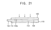
- FIGS. 17 to 21 are cross-sectional views illustrating a method of assembling the portable display device in FIG. 16 .
- a resin may be formed on the boundary line between the display region 112 and the drive circuit region 114 of the display panel 110.
- an ultraviolet light may be irradiated to the resin to form the blocking member 140e.
- the attaching member 130 including a resin may be coated on the display region 112 of the display panel 110.
- the blocking member 140 on the boundary line between the display region 112 and the drive circuit region 114 may block the resin, so that the resin may not infiltrate into the drive circuit region 114.
- the window 120 may be arranged on the attaching member 130.
- an ultraviolet light may be irradiated to the resin until the resin may be annealed to firmly attach the window 120 and the display panel 130 to each other via the annealed attaching member 130, thereby completing the portable display device 100e.
- the blocking member may be arranged on only the boundary line between the display region and the drive circuit region of the display panel.
- flows of the attaching member may be readily controlled using the blocking member having a simple structure to prevent the infiltration of the attaching member into the drive circuit region.
- the portable display device may be assembled by a simple process and a low cost.
Landscapes
- Physics & Mathematics (AREA)
- Nonlinear Science (AREA)
- Optics & Photonics (AREA)
- Engineering & Computer Science (AREA)
- General Physics & Mathematics (AREA)
- Mathematical Physics (AREA)
- Chemical & Material Sciences (AREA)
- Crystallography & Structural Chemistry (AREA)
- Microelectronics & Electronic Packaging (AREA)
- Manufacturing & Machinery (AREA)
- Computer Networks & Wireless Communication (AREA)
- Signal Processing (AREA)
- Theoretical Computer Science (AREA)
- Devices For Indicating Variable Information By Combining Individual Elements (AREA)
- Telephone Set Structure (AREA)
- Liquid Crystal (AREA)
Abstract

Description
- The present invention generally relates to a portable display device and a method of assembling the same.
- Generally, a portable display device such as a cellular phone may include a display panel and a window. The window may be attached to the display panel using an attaching member such as a resin. Because the non-hardened resin may have the potential of flowing, a process for controlling flows of the resin coated on the display panel may be required. That is, controlling resin flows may prevent the resin from being spilled from the display panel.
- A barrier may be formed at four sides of the display panel to prevent the spill of the resin from the display panel. Particularly, the barrier may include a resin different from the resin used for the attachment member.
- However, a process for coating the resin and a process for annealing the resin is required. Thus, a process for assembling the portable display device may be complicated.
- Further, because the resin used for the barrier may be expensive, a cost for manufacturing the portable display device may be increased.
- Example embodiments relate to a portable display device such as a cellular phone, and a method of assembling the portable display device.
- Example embodiments provide a portable display device that may be capable of controlling flows of a resin with a simple and cheap structure.
- Example embodiments provide a method of assembling the above-mentioned portable display device.
- According to one aspect of example embodiments, there is provided a portable display device. The portable display device may include a display panel, a window, an attaching member and a blocking member. The display panel may have a drive circuit region and a display region. The window may be positioned facing to the display panel.
- The attaching member may be interposed between the display region of the display panel and the window to attach the display panel to the window. The blocking member may be arranged on a boundary line between the drive circuit region and the display region to prevent the attaching member from infiltrating into the drive circuit region.
- In example embodiments, the drive circuit region may be located adjacent to only one side surface of the display panel. The blocking member may be wholly arranged on the boundary line. The blocking member may be parallel to the side surface of the display panel to which the drive circuit region may be located adjacent.
- In example embodiments, the portable display device may further include a flexible printed circuit (FPC) arranged in the drive circuit region. The blocking member may be partially arranged on the boundary line to prevent the attaching member from infiltrating into the FPC.
- In example embodiments, the blocking member may include a main blocking portion configured to cover a surface of the FPC exposed to the display region.
- In example embodiments, the blocking member may further include an auxiliary blocking portion extended from the main blocking portion to cover both side surfaces of the FPC at both sides of the exposed surface.
- In example embodiments, the display panel may further have a second drive circuit region. The portable display device may further include a second blocking member. The second blocking member may be arranged on a boundary line between the display region and the second drive circuit region to prevent the attaching member from infiltrating into the second drive circuit region.
- In example embodiments, the portable display device may further include a second FPC arranged in the second drive circuit region. The second blocking member may be partially arranged on the boundary line to prevent the attaching member from infiltrating into the second FPC.
- In example embodiments, the blocking member may include a transparent material.
- In example embodiments, the blocking member may include a double-sided adhesive tape.
- In example embodiments, the attaching member may include a resin. The blocking member may include a resin having a viscosity higher than that of the resin used for the attaching member.
- According to another aspect of example embodiments, there is provided a portable display device. The portable display device may include a display panel, an FPC, a window, an attaching member and a blocking member. The FPC may be connected to the display panel. The window may be positioned facing to the display panel. The attaching member may be interposed between the display panel and the window to attach the display panel to the window. The blocking member may be configured to cover the FPC to prevent the attaching member from infiltrating into the FPC.
- In example embodiments, the blocking member may include a main blocking portion configured to cover a first side surface of the FPC oriented toward a central portion of the display panel.
- In example embodiments, the blocking member may further include an auxiliary blocking portion extended from the main blocking portion to cover both side surfaces of the FPC at both sides of the first side surface.
- According to still another aspect of example embodiments, there is provided a method of assembling a portable display device. In the method of assembling the portable display device, a blocking member may be formed on a boundary line between a drive circuit region and a display region of a display panel. An attaching member may be coated on the display region of the display panel blocked from the drive circuit region by the blocking member. A window may be attached to the display panel using the attaching member.
- In example embodiments, forming the blocking member may include attaching a double-sided adhesive tape to the boundary line.
- In example embodiments, forming the blocking member may include coating a resin on the boundary line, and annealing the resin.
- In example embodiments, coating the attaching member may include coating a resin.
- In example embodiments, the method may further include annealing the attaching member.
- In example embodiments, annealing the attaching member may include irradiating an ultraviolet light to the attaching member.
- According to yet still another aspect of example embodiments, there is provided a method of assembling a portable display device. In the method of assembling the portable display device, a blocking member may cover a FPC connected to a display panel. An attaching member may be coated on the display panel. A window may be attached to the display panel using the attaching member.
- In example embodiments, forming the blocking member may include attaching a double-sided adhesive tape to the FPC.
- In example embodiments, the method may further include annealing the attaching member.
- In example embodiments, annealing the attaching member may include irradiating an ultraviolet light to the attaching member.
- According to example embodiments, the blocking member may be arranged on only the boundary line between the display region and the drive circuit region of the display panel. Thus, flows of the attaching member may be readily controlled using the blocking member having a simple structure to prevent the infiltration of the attaching member into the drive circuit region. As a result, the portable display device may be assembled by a simple process and a low cost.
- A more complete appreciation of the invention, and many of the attendant advantages thereof, will be readily apparent as the same becomes better understood by reference to the following detailed description when considered in conjunction with the accompanying drawings, in which like reference symbols indicate the same or similar components, wherein::
-
FIG. 1 is a front view illustrating a portable display device in accordance with example embodiments; -
FIG. 2 is a cross-sectional view taken along a line II-II' inFIG. 1 ; -
FIG. 3 is a cross-sectional view taken along a line III-III' inFIG. 1 ; -
FIGS. 4 to 7 are cross-sectional views illustrating a method of assembling the portable display device inFIG. 1 ; -
FIG. 8 is a front view illustrating a portable display device in accordance with example embodiments; -
FIG. 9 is a cross-sectional view taken along a line IX-IX' inFIG. 8 ; -
FIG. 10 is a cross-sectional view taken along a line X-X' inFIG. 8 ; -
FIG. 11 is a front view illustrating a portable display device in accordance with example embodiments; -
FIG. 12 is a cross-sectional view taken along a line XII-XII' inFIG. 11 ; -
FIG. 13 is a cross-sectional view taken along a line XIII-XIII' inFIG. 11 ; -
FIG. 14 is a front view illustrating a portable display device in accordance with example embodiments; -
FIG. 15 is a front view illustrating a portable display device in accordance with example embodiments; -
FIG. 16 is a front view illustrating a portable display device in accordance with example embodiments; and -
FIGS. 17 to 21 are cross-sectional views illustrating a method of assembling the portable display device inFIG. 16 . - In the drawings, the sizes and relative sizes of layers and regions may be exaggerated for clarity.
-
FIG. 1 is a front view illustrating a portable display device in accordance with example embodiments,FIG. 2 is a cross-sectional view taken along a line II-II' inFIG. 1 , andFIG. 3 is a cross-sectional view taken along a line III-III' inFIG. 1 . - Referring to
FIGS. 1 to 3 , aportable display device 100 of this example embodiment may include adisplay panel 110, awindow 120, an attachingmember 130 and a blockingmember 140. - In example embodiments, the
display panel 110 may have a rectangular cross-section. Thus, thedisplay panel 110 may have four side surfaces. Further, thedisplay panel 110 may have adisplay region 112 and adrive circuit region 114. Thedisplay panel 110 may include a liquid crystal display (LCD) panel, a plasma display panel, an organic light emitting display (OLED) panel, etc. - In example embodiments, in
FIG. 1 , thedrive circuit region 114 may correspond to a single region having a rectangular shape that may be positioned adjacent to a lower surface of thedisplay panel 110. Thedisplay region 112 may correspond to the rest region of thedisplay panel 110 except for thedrive circuit region 114. Shapes, sizes, positions, etc., of thedrive circuit region 114 may vary in accordance with kinds of theportable display device 100. - A flexible printed circuit (FPC) 150 may be arranged in the
drive circuit region 114. TheFPC 150 may apply electrical signals to thedisplay region 112. Thus, theFPC 150 may be exposed to thedisplay region 112. - The
window 120 may be arranged over thedisplay panel 110. Thewindow 120 may be attached to thedisplay panel 110 using the attachingmember 130. Thus, the attachingmember 130 may be interposed between thewindow 120 and thedisplay panel 110. In example embodiments, the attachingmember 130 may be located in only thedisplay region 112. That is, the attachingmember 130 may not be arranged in thedrive circuit region 114. - In example embodiments, the attaching
member 130 may include an insulating resin. The attachingmember 130 may be formed by coating a flowable resin between thedisplay panel 110 and thewindow 120, and by annealing the flowable resin. Thus, the flowable resin before annealing may flow from thedisplay region 112 toward thedrive circuit region 114. - The blocking
member 140 may be arranged on a boundary line between thedisplay region 112 and thedrive circuit region 114. The blockingmember 140 may prevent the flowable region in thedisplay region 112 from infiltrating into thedrive circuit region 114. Particularly, the blockingmember 140 may prevent the insulating resin from being smeared on the flexible printed circuit (FPC) 150 in thedrive circuit region 114. - In example embodiments, the blocking
member 140 may not surround the four side surfaces of thedisplay panel 110. The blockingmember 140 may be arranged on only the boundary line between thedisplay region 112 and thedrive circuit region 114. Therefore, the blockingmember 140 may have a long stripe shape substantially parallel with a lower side surface of thedisplay panel 110. Further, the blockingmember 140 may have a length substantially the same as that of the lower side surface of thedisplay panel 110. Thus, the blockingmember 140 may be extended along the whole boundary line between thedisplay region 112 and thedrive circuit region 114 to completely isolate thedrive circuit region 114 from thedisplay region 112. As a result, because the blockingmember 140 may block flows of the attachingmember 130 in thedisplay region 112 toward thedrive circuit region 114, the attachingmember 130 may not infiltrate into thedrive circuit region 114. - In example embodiments, in order to prevent a display quality of the
portable display device 100 from being deteriorated by the blockingmember 140, the blockingmember 140 may include a transparent material. - In example embodiments, the blocking
member 140 may include a double-sided adhesive tape. The double-sided adhesive tape may be cheap. Further, the double-sided adhesive tape may be easily attached. Therefore, theportable display device 100 may be readily assembled by a simple process and a low cost. Furthermore, the double-sided adhesive tape may have a function as to attach thedisplay panel 110 and thewindow 120 to each other. -
FIGS. 4 to 7 are cross-sectional views illustrating a method of assembling the portable display device inFIG. 1 . - Referring to
FIG. 4 , the blockingmember 140 may be formed on the boundary line between thedisplay region 112 and thedrive circuit region 114 of thedisplay panel 110. In example embodiments, the blockingmember 140 may include a transparent double-sided adhesive tape. Thus, the blockingmember 140 may be easily formed by attaching the double-sided adhesive tape on the boundary line between thedisplay region 112 and thedrive circuit region 114. - Referring to
FIG. 5 , the attachingmember 130 may be coated on thedisplay region 112 of thedisplay panel 110. In example embodiments, the attachingmember 130 may include an insulating resin. Because the insulating resin before annealing may have a flowable property, the resin may flow from thedisplay region 112 into thedrive circuit region 114. However, the blockingmember 140 on the boundary line between thedisplay region 112 and thedrive circuit region 114 may block the resin, so that the resin may not infiltrate into thedrive circuit region 114. - Referring to
FIG. 6 , thewindow 120 may be arranged on the attachingmember 130. Because the attachingmember 130 may not be annealed, thewindow 120 may not be attached to thedisplay panel 110. - Referring to
FIG. 7 , the attachingmember 130 may be annealed to firmly attach thewindow 120 and thedisplay panel 130 to each other via the annealed attachingmember 130, thereby completing theportable display device 100. In example embodiments, the attachingmember 130 may be annealed by irradiating an ultraviolet light to the resin. -
FIG. 8 is a front view illustrating a portable display device in accordance with example embodiments,FIG. 9 is a cross-sectional view taken along a line IX-IX' inFIG. 8 , andFIG. 10 is a cross-sectional view taken along a line X-X' inFIG. 8 . - A
portable display device 100a of this example embodiment may include elements substantially the same as those of theportable display device 100 inFIG. 1 except for a blockingmember 140a. Thus, the same reference numerals may refer to the same elements and any further illustrations with respect to the same element may be omitted herein for brevity. - Referring to
FIGS. 8 to 10 , the blockingmember 140a may block only theFPC 150. In example embodiments, the blockingmember 140a may be configured to cover a surface of theFPC 150 exposed to thedisplay region 112 of thedisplay panel 110. The blockingmember 140a may make contact with the surface of theFPC 150. Alternatively, the blockingmember 140a may be spaced apart from the surface of theFPC 150. - Therefore, the blocking
member 140a may be partially formed on the boundary line between thedisplay region 112 and thedrive circuit region 114 of thedisplay panel 110. That is, the blockingmember 140a may wholly isolate thedrive circuit region 114 from thedisplay region 112. The blockingmember 140a may block only the surface of theFPC 150 oriented toward thedisplay region 112. - According to this example embodiment, the blocking
member 140a may be configured to make contact with only the surface of theFPC 150, so that the blockingmember 140a may have a length shorter than that of the blockingmember 140 inFIG. 1 . Thus, a cost for forming the blockingmember 140a may be curtailed compared to the blockingmember 140 inFIG. 1 . - In example embodiments, a method of assembling the
portable display device 100a may include processes substantially the same as those illustrated with reference toFIGS. 4 to 7 . Thus, the method of assembling theportable display device 100a may be omitted herein for brevity. -
FIG. 11 is a front view illustrating a portable display device in accordance with example embodiments,FIG. 12 is a cross-sectional view taken along a line XII-XII' inFIG. 11 , andFIG. 13 is a cross-sectional view taken along a line XIII-XIII' inFIG. 11 . - A
portable display device 100b of this example embodiment may include elements substantially the same as those of theportable display device 100a inFIG. 8 except for a blockingmember 140b. Thus, the same reference numerals may refer to the same elements and any further illustrations with respect to the same element may be omitted herein for brevity. - Referring to
FIGS. 11 to 13 , the blockingmember 140b may include amain blocking portion 142b andauxiliary blocking portions main blocking portion 142b may be configured to cover the surface of theFPC 150 exposed to thedisplay region 112 of thedisplay panel 110. Theauxiliary blocking portions main blocking portion 142b to cover side surfaces of theFPC 150 at both sides of the exposed surface of theFPC 150. In example embodiments, themain blocking portion 142b and theauxiliary blocking portions FPC 150. Alternatively, themain blocking portion 142b and theauxiliary blocking member FPC 150. That is, the main blocking portion142b may have a shape substantially the same as that of the blockingmember 140a inFIG. 8 . Thus, the blockingmember 140b of this example embodiment may have a structure including the blockingmember 140a inFIG. 8 by adding theauxiliary blocking portions - According to this example embodiment, the
auxiliary blocking portions FPC 150 to prevent the attachingmember 130 from infiltrating into the side surfaces of the FPC 150.0 - In example embodiments, a method of assembling the
portable display device 100b may include processes substantially the same as those for assembling theportable display device 100a inFIG. 8 except for a process for forming the blockingmember 140b. Thus, the method of assembling theportable display device 100b may be omitted herein for brevity. -
FIG. 14 is a front view illustrating a portable display device in accordance with example embodiments. - Referring to
FIG. 14 , aportable display device 100c of this example embodiment may include adisplay panel 110, awindow 120, an attachingmember 130, afirst blocking member 140 and asecond blocking member 140c. - In example embodiments, the
display panel 110 may have asingle display region 112, a firstdrive circuit region 114 and a seconddrive circuit region 114c. The firstdrive circuit region 114 may correspond to a region adjacent to a lower side surface of thedisplay panel 110. The seconddrive circuit region 114c may correspond to a region adjacent to a right side surface of thedisplay panel 110. Thus, the firstdrive circuit region 114 and the seconddrive circuit region 114c may form a perpendicularly bent shape. - A
first FPC 150 may be arranged in the firstdrive circuit region 114. Asecond FPC 150c may be arranged in the seconddrive circuit region 114c. - The
window 120 may be positioned over thedisplay panel 110. Thewindow 120 may be attached to thedisplay panel 110 using the attachingmember 130. - The
first blocking member 140 may be arranged on a boundary line between thedisplay region 112 and the firstdrive circuit region 114. Thefirst blocking member 140 may prevent the flowable resin of the attachingmember 130 from infiltrating into the firstdrive circuit region 114 from thedisplay region 112. - The
second blocking member 140c may be arranged on a boundary line between thedisplay region 112 and the seconddrive circuit region 114c. Thesecond blocking member 140c may prevent the flowable resin of the attachingmember 130 from infiltrating into the seconddrive circuit region 114c from thedisplay region 112. - Alternatively, the
first blocking member 140 and thesecond blocking member 140c may have a shape substantially the same as that of the blockingmember 140a inFIG. 8 or the blockingmember 140b inFIG. 11 . - In example embodiments, a method of assembling the
portable display device 100c may include processes substantially the same as those illustrated with reference toFIGS. 4 to 7 except for further including a process for forming thesecond blocking member 140c. Thus, the method of assembling theportable display device 100c may be omitted herein for brevity. -
FIG. 15 is a front view illustrating a portable display device in accordance with example embodiments. - A
portable display device 100d of this example embodiment may include elements substantially the same as those of theportable display device 100c inFIG. 14 except for a position of a seconddrive circuit region 114d. Thus, the same reference numerals may refer to the same elements and any further illustrations with respect to the same element may be omitted herein for brevity. - Referring to
FIG. 15 , the seconddrive circuit region 114d may be positioned adjacent to an upper side surface of thedisplay panel 110. That is, the seconddrive circuit region 114d may be arranged facing to the firstdrive circuit region 114. - In example embodiments, a method of assembling the
portable display device 100d may include processes substantially the same as those for assembling theportable display device 100c inFIG. 14 except for changing the position of thesecond blocking member 140d. Thus, the method of assembling theportable display device 100d may be omitted herein for brevity. -
FIG. 16 is a front view illustrating a portable display device in accordance with example embodiments. - A
portable display device 100e of this example embodiment may include elements substantially the same as those of theportable display device 100 inFIG. 1 except for a material of a blockingmember 140e. Thus, the same reference numerals may refer to the same elements and any further illustrations with respect to the same element may be omitted herein for brevity. - Referring to
FIG. 16 , the blockingmember 140e may include a resin. In example embodiments, the resin of the blockingmember 140e may not have a high viscosity, so that the resin of the blockingmember 140e may have a viscosity higher than that of the resin for the attachingmember 130. - In example embodiments, because the blocking
member 140e may include the resin, the blockingmember 140e may be expensive compared to the double-sided adhesive tapes in above-mentioned example embodiments. However, the blockingmember 140e may be arranged along only a single side surface of thedisplay panel 110, not all of the four side surfaces of thedisplay panel 110. Thus, a cost for forming the blockingmember 140e may be comparatively lower than that for forming a blocking member arranged along the four side surfaces of thedisplay panel 110. -
FIGS. 17 to 21 are cross-sectional views illustrating a method of assembling the portable display device inFIG. 16 . - Referring to
FIG. 17 , a resin may be formed on the boundary line between thedisplay region 112 and thedrive circuit region 114 of thedisplay panel 110. - Referring to
FIG. 18 , an ultraviolet light may be irradiated to the resin to form the blockingmember 140e. - Referring to
FIG. 19 , the attachingmember 130 including a resin may be coated on thedisplay region 112 of thedisplay panel 110. The blockingmember 140 on the boundary line between thedisplay region 112 and thedrive circuit region 114 may block the resin, so that the resin may not infiltrate into thedrive circuit region 114. - Referring to
FIG. 20 , thewindow 120 may be arranged on the attachingmember 130. - Referring to
FIG. 21 , an ultraviolet light may be irradiated to the resin until the resin may be annealed to firmly attach thewindow 120 and thedisplay panel 130 to each other via the annealed attachingmember 130, thereby completing theportable display device 100e. - According to some example embodiments, the blocking member may be arranged on only the boundary line between the display region and the drive circuit region of the display panel. Thus, flows of the attaching member may be readily controlled using the blocking member having a simple structure to prevent the infiltration of the attaching member into the drive circuit region. As a result, the portable display device may be assembled by a simple process and a low cost.
- The foregoing is illustrative of example embodiments, and is not to be construed as limiting thereof. Although a few example embodiments have been described, those skilled in the art will readily appreciate that many modifications are possible in the example embodiments without materially departing from the scope of the invention as defined by the claims.
Claims (15)
- A portable display device, comprising:a display panel having a drive circuit region and a display region;a window arranged facing the display panel;an attaching member interposed between the display region of the display panel and the window to attach the window to the display panel; anda blocking member arranged on a boundary line between the drive circuit region and the display region to prevent the attaching member from infiltrating into the drive circuit region.
- The portable display device recited in claim 1, wherein the drive circuit region is arranged adjacent to only one side surface of the display panel, and the blocking member is wholly arranged on the boundary line and parallel to the side surface of the display panel.
- The portable display device recited in claim 1 or 2, further comprising:a flexible printed circuit FPC arranged in the drive circuit region,wherein the blocking member is partially arranged on the boundary line to prevent the attaching member from infiltrating into the FPC.
- The portable display device recited in claim 3, wherein the blocking member comprises a main blocking portion configured to cover a surface of the FPC exposed to the display region.
- The portable display device recited in claim 4, wherein the blocking member further comprises an auxiliary blocking portion extended from the main blocking portion to cover side surfaces of the FPC at both sides of the exposed surface of the FPC.
- The portable display device recited in any one of the preceding claims, wherein the display panel further has a second drive circuit region,
further comprising a second blocking member arranged on a boundary line between the display region and the second drive circuit region to prevent the attaching member from infiltrating into the second drive circuit region. - The portable display device recited in claim 6, further comprising a second FPC arranged in the second drive circuit region,
wherein the second blocking member is partially arranged on the boundary line to prevent the attaching member from infiltrating into the second FPC. - The portable display device recited in any one of the preceding claims, wherein the blocking member comprises a transparent material.
- The portable display device recited in any one of the preceding claims, wherein the blocking member comprises a double-sided adhesive tape
- The portable display device recited in any one of claims 1 to 8, wherein the attaching member comprises a resin, and the blocking member comprises a resin having a viscosity higher than that of the resin for the attaching member.
- A method of assembling a portable display device, the method comprising:forming a blocking member on a boundary line between a drive circuit region and a display region of a display panel;forming an attaching member on the display region isolated from the drive circuit region by the blocking member; andattaching a window to the display panel using the attaching member.
- The method recited in claim 13, wherein forming the blocking member comprises attaching a double-sided adhesive tape on the boundary line.
- The method recited in claim 11, wherein forming the blocking member comprises:coating a resin on the boundary line; andannealing the resin.
- The method recited in claim 11, wherein forming the attaching member comprises coating a resin on the display region.
- The method recited in claim 11, further comprising annealing the attaching member, wherein annealing the attaching member may comprise irradiating an ultraviolet light to the attaching member.
Applications Claiming Priority (1)
| Application Number | Priority Date | Filing Date | Title |
|---|---|---|---|
| KR1020120054723A KR102037700B1 (en) | 2012-05-23 | 2012-05-23 | Portable display device and method of assembling the same |
Publications (1)
| Publication Number | Publication Date |
|---|---|
| EP2667246A1 true EP2667246A1 (en) | 2013-11-27 |
Family
ID=48190101
Family Applications (1)
| Application Number | Title | Priority Date | Filing Date |
|---|---|---|---|
| EP13164066.6A Withdrawn EP2667246A1 (en) | 2012-05-23 | 2013-04-17 | Portable display device and method of assembling the same |
Country Status (6)
| Country | Link |
|---|---|
| US (1) | US9661774B2 (en) |
| EP (1) | EP2667246A1 (en) |
| JP (1) | JP2013246432A (en) |
| KR (1) | KR102037700B1 (en) |
| CN (2) | CN103426365B (en) |
| TW (1) | TW201349963A (en) |
Cited By (1)
| Publication number | Priority date | Publication date | Assignee | Title |
|---|---|---|---|---|
| EP3582064A1 (en) * | 2018-06-15 | 2019-12-18 | Samsung Electronics Co., Ltd. | Display device and electronic device including the same |
Families Citing this family (5)
| Publication number | Priority date | Publication date | Assignee | Title |
|---|---|---|---|---|
| KR102037700B1 (en) * | 2012-05-23 | 2019-10-30 | 삼성디스플레이 주식회사 | Portable display device and method of assembling the same |
| KR101984245B1 (en) | 2012-12-13 | 2019-05-31 | 삼성디스플레이 주식회사 | Organic light emitting diode display |
| KR102293728B1 (en) | 2014-07-04 | 2021-08-27 | 삼성디스플레이 주식회사 | Display apparatus |
| KR102263982B1 (en) | 2014-10-20 | 2021-06-11 | 엘지디스플레이 주식회사 | Display apparatus |
| CN118736966B (en) * | 2024-06-27 | 2025-11-14 | 昆山国显光电有限公司 | Cover plate, display device, and method for manufacturing the cover plate |
Citations (3)
| Publication number | Priority date | Publication date | Assignee | Title |
|---|---|---|---|---|
| US20050155704A1 (en) * | 2004-01-16 | 2005-07-21 | Eastman Kodak Company | Method of making an OLED display device with enhanced optical and mechanical properties |
| US20090086123A1 (en) * | 2007-09-28 | 2009-04-02 | Casio Computer Co., Ltd. | Display device integral with protection plate, and display apparatus using the same |
| US20100245707A1 (en) * | 2009-03-27 | 2010-09-30 | Casio Computer Co., Ltd. | Protection plate integrated display apparatus |
Family Cites Families (16)
| Publication number | Priority date | Publication date | Assignee | Title |
|---|---|---|---|---|
| JP3531633B2 (en) * | 2000-09-14 | 2004-05-31 | セイコーエプソン株式会社 | Liquid crystal devices and electronic equipment |
| JP3841040B2 (en) * | 2002-10-25 | 2006-11-01 | セイコーエプソン株式会社 | ELECTRO-OPTICAL DEVICE, MANUFACTURING METHOD THEREOF, AND ELECTRONIC DEVICE |
| US7691685B2 (en) * | 2004-01-26 | 2010-04-06 | Semiconductor Energy Laboratory Co., Ltd. | Method for manufacturing semiconductor device |
| US7753751B2 (en) | 2004-09-29 | 2010-07-13 | Semiconductor Energy Laboratory Co., Ltd. | Method of fabricating the display device |
| US20060111009A1 (en) | 2004-11-24 | 2006-05-25 | Taiwan Micro Display Corp. | System and method of batch manufacturing a display face plate array |
| KR101138261B1 (en) | 2005-06-29 | 2012-04-24 | 엘지디스플레이 주식회사 | liquid crystal display device |
| KR101415567B1 (en) | 2007-12-11 | 2014-07-04 | 삼성디스플레이 주식회사 | Flexible printed circuit and display device including the same |
| KR20090089586A (en) | 2008-02-19 | 2009-08-24 | 삼성모바일디스플레이주식회사 | Organic light emitting display |
| KR20100004292A (en) | 2008-07-03 | 2010-01-13 | 엘지이노텍 주식회사 | Display device |
| KR101545028B1 (en) | 2009-07-29 | 2015-08-18 | 엘지디스플레이 주식회사 | Backlight unit and liquid crystal display device having the same |
| KR20110055089A (en) | 2009-11-19 | 2011-05-25 | 엘지전자 주식회사 | Plasma Display and Multi Plasma Display |
| CN102194379A (en) | 2010-03-02 | 2011-09-21 | 耀众科技股份有限公司 | Flexible display |
| KR101117399B1 (en) | 2010-05-11 | 2012-03-07 | 주식회사 에이치엔에이치글로벌리소스 | Portable display device and method for assembling the same |
| KR101247680B1 (en) | 2010-12-06 | 2013-04-01 | 엘지디스플레이 주식회사 | Electrophoretic Display Device and Method for Manufacturing thereof |
| KR101753775B1 (en) | 2010-12-15 | 2017-07-05 | 삼성디스플레이 주식회사 | An liquid crystal display device and the manufacturing method thereof |
| KR102037700B1 (en) | 2012-05-23 | 2019-10-30 | 삼성디스플레이 주식회사 | Portable display device and method of assembling the same |
-
2012
- 2012-05-23 KR KR1020120054723A patent/KR102037700B1/en active Active
- 2012-11-20 JP JP2012254449A patent/JP2013246432A/en active Pending
-
2013
- 2013-02-25 US US13/775,632 patent/US9661774B2/en active Active
- 2013-03-19 TW TW102109760A patent/TW201349963A/en unknown
- 2013-03-19 CN CN201310087089.5A patent/CN103426365B/en active Active
- 2013-03-19 CN CN2013201241557U patent/CN203150021U/en not_active Expired - Lifetime
- 2013-04-17 EP EP13164066.6A patent/EP2667246A1/en not_active Withdrawn
Patent Citations (3)
| Publication number | Priority date | Publication date | Assignee | Title |
|---|---|---|---|---|
| US20050155704A1 (en) * | 2004-01-16 | 2005-07-21 | Eastman Kodak Company | Method of making an OLED display device with enhanced optical and mechanical properties |
| US20090086123A1 (en) * | 2007-09-28 | 2009-04-02 | Casio Computer Co., Ltd. | Display device integral with protection plate, and display apparatus using the same |
| US20100245707A1 (en) * | 2009-03-27 | 2010-09-30 | Casio Computer Co., Ltd. | Protection plate integrated display apparatus |
Cited By (2)
| Publication number | Priority date | Publication date | Assignee | Title |
|---|---|---|---|---|
| EP3582064A1 (en) * | 2018-06-15 | 2019-12-18 | Samsung Electronics Co., Ltd. | Display device and electronic device including the same |
| US11240921B2 (en) | 2018-06-15 | 2022-02-01 | Samsung Electronics Co., Ltd. | Display device and electronic device including the same |
Also Published As
| Publication number | Publication date |
|---|---|
| CN203150021U (en) | 2013-08-21 |
| TW201349963A (en) | 2013-12-01 |
| US9661774B2 (en) | 2017-05-23 |
| CN103426365A (en) | 2013-12-04 |
| JP2013246432A (en) | 2013-12-09 |
| KR20130131010A (en) | 2013-12-03 |
| US20130314881A1 (en) | 2013-11-28 |
| KR102037700B1 (en) | 2019-10-30 |
| CN103426365B (en) | 2017-08-25 |
Similar Documents
| Publication | Publication Date | Title |
|---|---|---|
| EP2667246A1 (en) | Portable display device and method of assembling the same | |
| EP3182476B1 (en) | Organic light emitting display device | |
| US9684404B2 (en) | Display device | |
| US9690150B2 (en) | Electro-optical display device | |
| KR20160117230A (en) | Display device | |
| WO2009069476A1 (en) | Electronic device, display apparatus and method for manufacturing electronic device | |
| US20180198089A1 (en) | Display device | |
| GB0811058D0 (en) | Sealed switchable glazing | |
| JP2019511406A5 (en) | ||
| KR20150137239A (en) | Organic light emitting display device and manufacturing method of the same | |
| US9564895B2 (en) | Touch key assembly and display device including the touch key assembly | |
| US10860057B2 (en) | Display panel and display apparatus thereof | |
| US9525154B2 (en) | Display device | |
| KR101721736B1 (en) | Display device | |
| CN110782780B (en) | Adhesive tape structure, display panel using same and display device | |
| KR20170112128A (en) | Film for Electrophoretic Display Device and Electrophoretic Display Device | |
| CN105372899A (en) | Lower electrode substrate for sectional electrophoretic display device and method of manufacturing the same | |
| EP3669116A1 (en) | Flexible light emitting system | |
| KR20160005271A (en) | Display apparatus | |
| US10483437B2 (en) | Display device | |
| EP2913860B1 (en) | Lighting panel | |
| KR20170080911A (en) | Display device | |
| KR20100064499A (en) | Flat panel display device | |
| KR102221608B1 (en) | Circuit board and liquid crystal display | |
| KR20200036410A (en) | Organic light emitting display device |
Legal Events
| Date | Code | Title | Description |
|---|---|---|---|
| PUAI | Public reference made under article 153(3) epc to a published international application that has entered the european phase |
Free format text: ORIGINAL CODE: 0009012 |
|
| AK | Designated contracting states |
Kind code of ref document: A1 Designated state(s): AL AT BE BG CH CY CZ DE DK EE ES FI FR GB GR HR HU IE IS IT LI LT LU LV MC MK MT NL NO PL PT RO RS SE SI SK SM TR |
|
| AX | Request for extension of the european patent |
Extension state: BA ME |
|
| 17P | Request for examination filed |
Effective date: 20140527 |
|
| RBV | Designated contracting states (corrected) |
Designated state(s): AL AT BE BG CH CY CZ DE DK EE ES FI FR GB GR HR HU IE IS IT LI LT LU LV MC MK MT NL NO PL PT RO RS SE SI SK SM TR |
|
| RAP1 | Party data changed (applicant data changed or rights of an application transferred) |
Owner name: SAMSUNG DISPLAY CO., LTD. |
|
| STAA | Information on the status of an ep patent application or granted ep patent |
Free format text: STATUS: EXAMINATION IS IN PROGRESS |
|
| 17Q | First examination report despatched |
Effective date: 20170912 |
|
| STAA | Information on the status of an ep patent application or granted ep patent |
Free format text: STATUS: THE APPLICATION IS DEEMED TO BE WITHDRAWN |
|
| 18D | Application deemed to be withdrawn |
Effective date: 20180123 |