EP2663169A1 - Retaining and contacting element, contacting arrangement and method for establishing a contacting arrangement - Google Patents
Retaining and contacting element, contacting arrangement and method for establishing a contacting arrangement Download PDFInfo
- Publication number
- EP2663169A1 EP2663169A1 EP12177355.0A EP12177355A EP2663169A1 EP 2663169 A1 EP2663169 A1 EP 2663169A1 EP 12177355 A EP12177355 A EP 12177355A EP 2663169 A1 EP2663169 A1 EP 2663169A1
- Authority
- EP
- European Patent Office
- Prior art keywords
- retaining
- moulding
- section
- web
- contacting element
- Prior art date
- Legal status (The legal status is an assumption and is not a legal conclusion. Google has not performed a legal analysis and makes no representation as to the accuracy of the status listed.)
- Withdrawn
Links
Images

Classifications
-
- H—ELECTRICITY
- H01—ELECTRIC ELEMENTS
- H01R—ELECTRICALLY-CONDUCTIVE CONNECTIONS; STRUCTURAL ASSOCIATIONS OF A PLURALITY OF MUTUALLY-INSULATED ELECTRICAL CONNECTING ELEMENTS; COUPLING DEVICES; CURRENT COLLECTORS
- H01R43/00—Apparatus or processes specially adapted for manufacturing, assembling, maintaining, or repairing of line connectors or current collectors or for joining electric conductors
- H01R43/16—Apparatus or processes specially adapted for manufacturing, assembling, maintaining, or repairing of line connectors or current collectors or for joining electric conductors for manufacturing contact members, e.g. by punching and by bending
-
- H—ELECTRICITY
- H01—ELECTRIC ELEMENTS
- H01R—ELECTRICALLY-CONDUCTIVE CONNECTIONS; STRUCTURAL ASSOCIATIONS OF A PLURALITY OF MUTUALLY-INSULATED ELECTRICAL CONNECTING ELEMENTS; COUPLING DEVICES; CURRENT COLLECTORS
- H01R12/00—Structural associations of a plurality of mutually-insulated electrical connecting elements, specially adapted for printed circuits, e.g. printed circuit boards [PCB], flat or ribbon cables, or like generally planar structures, e.g. terminal strips, terminal blocks; Coupling devices specially adapted for printed circuits, flat or ribbon cables, or like generally planar structures; Terminals specially adapted for contact with, or insertion into, printed circuits, flat or ribbon cables, or like generally planar structures
- H01R12/50—Fixed connections
- H01R12/51—Fixed connections for rigid printed circuits or like structures
- H01R12/52—Fixed connections for rigid printed circuits or like structures connecting to other rigid printed circuits or like structures
-
- H—ELECTRICITY
- H01—ELECTRIC ELEMENTS
- H01B—CABLES; CONDUCTORS; INSULATORS; SELECTION OF MATERIALS FOR THEIR CONDUCTIVE, INSULATING OR DIELECTRIC PROPERTIES
- H01B7/00—Insulated conductors or cables characterised by their form
- H01B7/08—Flat or ribbon cables
- H01B7/0846—Parallel wires, fixed upon a support layer
-
- H—ELECTRICITY
- H01—ELECTRIC ELEMENTS
- H01R—ELECTRICALLY-CONDUCTIVE CONNECTIONS; STRUCTURAL ASSOCIATIONS OF A PLURALITY OF MUTUALLY-INSULATED ELECTRICAL CONNECTING ELEMENTS; COUPLING DEVICES; CURRENT COLLECTORS
- H01R12/00—Structural associations of a plurality of mutually-insulated electrical connecting elements, specially adapted for printed circuits, e.g. printed circuit boards [PCB], flat or ribbon cables, or like generally planar structures, e.g. terminal strips, terminal blocks; Coupling devices specially adapted for printed circuits, flat or ribbon cables, or like generally planar structures; Terminals specially adapted for contact with, or insertion into, printed circuits, flat or ribbon cables, or like generally planar structures
- H01R12/70—Coupling devices
- H01R12/71—Coupling devices for rigid printing circuits or like structures
- H01R12/72—Coupling devices for rigid printing circuits or like structures coupling with the edge of the rigid printed circuits or like structures
- H01R12/722—Coupling devices for rigid printing circuits or like structures coupling with the edge of the rigid printed circuits or like structures coupling devices mounted on the edge of the printed circuits
- H01R12/725—Coupling devices for rigid printing circuits or like structures coupling with the edge of the rigid printed circuits or like structures coupling devices mounted on the edge of the printed circuits containing contact members presenting a contact carrying strip, e.g. edge-like strip
-
- H—ELECTRICITY
- H01—ELECTRIC ELEMENTS
- H01R—ELECTRICALLY-CONDUCTIVE CONNECTIONS; STRUCTURAL ASSOCIATIONS OF A PLURALITY OF MUTUALLY-INSULATED ELECTRICAL CONNECTING ELEMENTS; COUPLING DEVICES; CURRENT COLLECTORS
- H01R12/00—Structural associations of a plurality of mutually-insulated electrical connecting elements, specially adapted for printed circuits, e.g. printed circuit boards [PCB], flat or ribbon cables, or like generally planar structures, e.g. terminal strips, terminal blocks; Coupling devices specially adapted for printed circuits, flat or ribbon cables, or like generally planar structures; Terminals specially adapted for contact with, or insertion into, printed circuits, flat or ribbon cables, or like generally planar structures
- H01R12/70—Coupling devices
- H01R12/71—Coupling devices for rigid printing circuits or like structures
- H01R12/72—Coupling devices for rigid printing circuits or like structures coupling with the edge of the rigid printed circuits or like structures
- H01R12/73—Coupling devices for rigid printing circuits or like structures coupling with the edge of the rigid printed circuits or like structures connecting to other rigid printed circuits or like structures
-
- H—ELECTRICITY
- H05—ELECTRIC TECHNIQUES NOT OTHERWISE PROVIDED FOR
- H05K—PRINTED CIRCUITS; CASINGS OR CONSTRUCTIONAL DETAILS OF ELECTRIC APPARATUS; MANUFACTURE OF ASSEMBLAGES OF ELECTRICAL COMPONENTS
- H05K3/00—Apparatus or processes for manufacturing printed circuits
- H05K3/36—Assembling printed circuits with other printed circuits
- H05K3/368—Assembling printed circuits with other printed circuits parallel to each other
-
- H—ELECTRICITY
- H05—ELECTRIC TECHNIQUES NOT OTHERWISE PROVIDED FOR
- H05K—PRINTED CIRCUITS; CASINGS OR CONSTRUCTIONAL DETAILS OF ELECTRIC APPARATUS; MANUFACTURE OF ASSEMBLAGES OF ELECTRICAL COMPONENTS
- H05K2201/00—Indexing scheme relating to printed circuits covered by H05K1/00
- H05K2201/04—Assemblies of printed circuits
- H05K2201/042—Stacked spaced PCBs; Planar parts of folded flexible circuits having mounted components in between or spaced from each other
-
- Y—GENERAL TAGGING OF NEW TECHNOLOGICAL DEVELOPMENTS; GENERAL TAGGING OF CROSS-SECTIONAL TECHNOLOGIES SPANNING OVER SEVERAL SECTIONS OF THE IPC; TECHNICAL SUBJECTS COVERED BY FORMER USPC CROSS-REFERENCE ART COLLECTIONS [XRACs] AND DIGESTS
- Y10—TECHNICAL SUBJECTS COVERED BY FORMER USPC
- Y10T—TECHNICAL SUBJECTS COVERED BY FORMER US CLASSIFICATION
- Y10T29/00—Metal working
- Y10T29/49—Method of mechanical manufacture
- Y10T29/49002—Electrical device making
- Y10T29/49117—Conductor or circuit manufacturing
- Y10T29/49204—Contact or terminal manufacturing
- Y10T29/49208—Contact or terminal manufacturing by assembling plural parts
-
- Y—GENERAL TAGGING OF NEW TECHNOLOGICAL DEVELOPMENTS; GENERAL TAGGING OF CROSS-SECTIONAL TECHNOLOGIES SPANNING OVER SEVERAL SECTIONS OF THE IPC; TECHNICAL SUBJECTS COVERED BY FORMER USPC CROSS-REFERENCE ART COLLECTIONS [XRACs] AND DIGESTS
- Y10—TECHNICAL SUBJECTS COVERED BY FORMER USPC
- Y10T—TECHNICAL SUBJECTS COVERED BY FORMER US CLASSIFICATION
- Y10T29/00—Metal working
- Y10T29/49—Method of mechanical manufacture
- Y10T29/49002—Electrical device making
- Y10T29/49117—Conductor or circuit manufacturing
- Y10T29/49204—Contact or terminal manufacturing
- Y10T29/49208—Contact or terminal manufacturing by assembling plural parts
- Y10T29/4921—Contact or terminal manufacturing by assembling plural parts with bonding
Definitions
- the invention relates to a retaining and contacting element, a contacting arrangement and a method for establishing a contacting arrangement.
- electronic printed circuit boards are multi-level stacked in housings, i.e. a plurality of printed circuit boards are stacked spaced from each other by means of separate retaining elements and contacted by means of respective electrical connection wires.
- the object is achieved by a retaining and contacting element according to claim 1, a contacting arrangement according to claim 13 and a method for contacting according to claim 15.
- a retaining and contacting element has a substantially U-shaped cross section comprising:
- At least one live hinge is arranged in the second moulding dividing the second moulding into at least two sections.
- Live hinges are hinges which are arranged as a single part with the two elements to be connected.
- Live hinges substantially consist of a wall connection with a reduced thickness, e.g. in the shape of a flexible reduction allowing a limited rotary motion of the connected parts.
- At least two live hinges are arranged in the second moulding dividing the second moulding into at least three sections.
- the live hinge or live hinges substantially runs/run in parallel with the second flange.
- the live hinge may be arranged at a lower side of the second moulding opposite the upper side, preferably as a wedge shaped notch cut into the lower side of the second moulding.
- the live hinge may be arranged as portions of reduced thickness by cutting a wedge shaped notch into the upper side of the second moulding or by cutting a respective wedge shaped notch into either side of the second moulding.
- the plurality of conductive paths extend over three neighbouring sections of the upper moulding divided by two live hinges, one of the sections adjacent the second flange, wherein the first section faces away from the web.
- the plurality of conductive paths extend from the second moulding over an outer face of the second flange to the web at least partially covering the web, wherein the second flange may face towards the web. This allows for retaining and contacting element with one live hinge or even without a live hinge.
- the retaining and contacting element comprises a first moulding extending from the first flange in parallel to the web. This improves the robustness of the retaining and contacting element as the first flange may be used to support an electric component to be contacted.
- the retaining and contacting element comprises or is made of plastics or a plastic compound, wherein the conductive paths are part of a conductive layer on the retaining and contacting element.
- first flange and/or the second flange are arranged at an angle between 90 degrees and 170 degrees with respect to the web. Smaller angles towards 90 degrees allow for higher precision in the distances between the electric components to be contacted by the retaining and contacting element. Angles, considerably greater than 90 degrees allow for tolerances in these distances and may improve the contacting reliability.
- the second live hinge is arranged in a distance from and in parallel to the first live hinge, wherein the distance substantially equals a height of the flanges.
- At least one retaining and contacting element in a contacting arrangement between at least two electrical components or electrical assemblies to be contacted at least one retaining and contacting element is arranged.
- the retaining and contacting element is at least partially or in sections coated with an electrically conductive layer.
- a method for establishing a contacting arrangement comprises:
- the resulting contacting arrangement according to the invention comprises:
- the electric components are arranged as electrical printed circuit boards.
- a conventional retaining element and a conventional contacting element are substituted by a combined retaining and contacting element so that a part count decreases.
- a conventional, expensive plug connector system for contacting neighbouring printed circuit boards may be replaced by a combined retaining and contacting element.
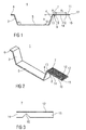
- Figure 1 is a schematic lateral view of a retaining and contacting element 1 for establishing a contacting arrangement 2 according to the invention which is illustrated in figure 4 .
- Figure 2 is a schematic perspective view of the retaining and contacting element 1
- the retaining and contacting element 1 exhibits a substantially U-shaped cross section with a first flange 3, a second flange 4 and a web 5, wherein the flanges 3, 4 extend from an upper side of the web 5.
- the retaining and contacting element preferably comprises or is made of plastics or a plastic compound.
- the web 5 substantially forms a flat base plane.
- the first flange 3 is arranged at a pre-determined angle ⁇ 1 with respect to the web 5 in a conventional manner. Preferably the value of the angle ⁇ 1 is between 90 degrees and 170 degrees.
- the first flange 3 is extended by a first moulding 6 arranged in parallel to the web 5 of the U-shaped cross section.
- first moulding 6 is arranged at an angle with respect to the first flange 3 facing away from the web 5.
- first moulding 6 may be arranged at an angle with respect to the first flange 3 facing towards the web 5.
- the second flange 4 is arranged at a pre-determined angle ⁇ 2 with respect to the web 5 in a conventional manner. Preferably the value of the angle ⁇ 2 is between 90 degrees and 170 degrees.
- the second flange 4 is extended by a second moulding 7 arranged in parallel to the web 5 of the U-shaped cross section.
- Live hinges 9, 10 are conventional hinges which are arranged as a single part with the two elements to be connected.
- Live hinges 9, 10 substantially consist of a wall connection with a reduced thickness, e.g. in the shape of a flexible reduction allowing a limited rotary motion of the connected parts.
- Figure 3 is a schematic view of the second live hinge 10 as a detail view of the second moulding 7 of the retaining and contacting element 1.
- the electrically conductive layer is preferably arranged as a plurality of single, conductive paths 12 arranged in parallel to each other. A longitudinal extension of the conductive paths 12 runs in parallel with the longitudinal extension of the web 5 between the flanges 3, 4.
- the first live hinge 9 runs in a pre-determined distance A 1 from the second flange 4 and is arranged in the second moulding 7 transversely with respect to the conductive paths 12 arranged in the upper side 11.
- the second live hinge 10 is arranged in the second moulding 7 in a pre-determined distance A 2 from and in parallel to the first live hinge 9.
- the distance A 2 between the two live hinges 9 and 10 equals a height H of the flanges 3 and 4.
- the second moulding 7 is divided into three sections 13, 14 and 15 by the two live hinges 9 and 10.
- the live hinges 9 and 10 are arranged as portions of reduced thickness by cutting a wedge shaped notch into the lower side 8 of the second moulding 7.
- the live hinges 9 and 10 could be arranged as portions of reduced thickness by cutting a wedge shaped notch into the upper side 11 of the second moulding 7 or by cutting a respective wedge shaped notch into either side of the second moulding 7.
- Figure 4 is a schematic lateral view of the contacting arrangement 2 according to the invention.
- Figure 5 is a schematic perspective view of a retaining and contacting element 1 arranged on a first electric component 16.
- the web 5 of the retaining and contacting element 1 is positively, non-positively and/or by adhesive bond attached to a first electric component 16.
- the first live hinge 9 is moved in such a manner that a first section 13 of the second moulding 7 remains in parallel to the web 5 and aligned within a plane with the first moulding 6 while a neighbouring second section 14 is arranged at a 90 degree angle with respect to this first section 13.
- the second live hinge 10 is moved in such a manner that a third section 15 of the second moulding 7 is arranged at a 90 degree angle with respect to the second section 14 towards the web 5.
- the third section 15 is aligned in the same spatial plane as the web 5.
- the conductive paths 12 of the electrically conductive layer on the sections 13, 14 and 15 are thus deformed so that the sections of the conductive paths 12 in the third section 15 of the second moulding 7 are located on a surface 17 of the first electric component 16 thus contacting the first electric component.
- a second electric component 19 is aligned substantially in parallel with the first electric component 16 and positively, non-positively and/or by adhesive bond attached on the upper side 18 of the first moulding 6 and on the upper side 11 of the first section 13 of the second moulding 7.
- the sections of the conductive path 12 arranged on the first section 13 contact the second electric component 19.
- the electric components 16, 19 are arranged as electrical printed circuit boards.
- a conventional retaining element and a conventional contacting element are substituted by a combined retaining and contacting element 1 so that a part count decreases.
- the second moulding 7 is arranged at an angle with respect to the second flange 4 facing away from the web 5.
- the second moulding 7 could be arranged at an angle with respect to the second flange 4 facing towards the web 5.
- the retaining and contacting element 1 could be arranged without or with only one live hinge 9, wherein the conductive paths 12 would extend over the first section 13, an outer face of the second flange 4 and at least a part of the web 5 adjacent the second flange 4.
Landscapes
- Engineering & Computer Science (AREA)
- Manufacturing & Machinery (AREA)
- Microelectronics & Electronic Packaging (AREA)
- Connector Housings Or Holding Contact Members (AREA)
Abstract
- a web (5),
- a first flange (3) and a second flange (4), wherein the flanges (3, 4) extend from an upper side of the web (5),
- a second moulding (7) extending from the second flange (4) in parallel to the web (5),
- a plurality of conductive paths (12) arranged at least on part of an upper side (11) of the second moulding (7), wherein a longitudinal extension of the conductive paths (12) runs in parallel with a longitudinal extension of the web (5).
Description
- The invention relates to a retaining and contacting element, a contacting arrangement and a method for establishing a contacting arrangement.
- Conventionally, electronic printed circuit boards are multi-level stacked in housings, i.e. a plurality of printed circuit boards are stacked spaced from each other by means of separate retaining elements and contacted by means of respective electrical connection wires.
- It is an object of the present invention to provide an improved retaining and contacting element, an improved contacting arrangement and an improved method for establishing a contacting arrangement.
- The object is achieved by a retaining and contacting element according to
claim 1, a contacting arrangement according toclaim 13 and a method for contacting according toclaim 15. - According to the invention a retaining and contacting element has a substantially U-shaped cross section comprising:
- a web,
- a first flange and a second flange, wherein the flanges extend from an upper side of the web,
- a second moulding extending from the second flange in parallel to the web,
- a plurality of conductive paths arranged at least on part of an upper side of the second moulding, wherein a longitudinal extension of the conductive paths runs in parallel with a longitudinal extension of the web. The longitudinal extension of the web in the context of this specification is the extension from the first flange to the second flange.
- In an exemplary embodiment at least one live hinge is arranged in the second moulding dividing the second moulding into at least two sections. Live hinges are hinges which are arranged as a single part with the two elements to be connected. Live hinges substantially consist of a wall connection with a reduced thickness, e.g. in the shape of a flexible reduction allowing a limited rotary motion of the connected parts.
- Preferably at least two live hinges are arranged in the second moulding dividing the second moulding into at least three sections.
- Preferably, the live hinge or live hinges substantially runs/run in parallel with the second flange.
- The live hinge may be arranged at a lower side of the second moulding opposite the upper side, preferably as a wedge shaped notch cut into the lower side of the second moulding. In alternative embodiments the live hinge may be arranged as portions of reduced thickness by cutting a wedge shaped notch into the upper side of the second moulding or by cutting a respective wedge shaped notch into either side of the second moulding.
- In an exemplary embodiment the plurality of conductive paths extend over three neighbouring sections of the upper moulding divided by two live hinges, one of the sections adjacent the second flange, wherein the first section faces away from the web.
- In an alternative embodiment the plurality of conductive paths extend from the second moulding over an outer face of the second flange to the web at least partially covering the web, wherein the second flange may face towards the web. This allows for retaining and contacting element with one live hinge or even without a live hinge.
- In an exemplary embodiment the retaining and contacting element comprises a first moulding extending from the first flange in parallel to the web. This improves the robustness of the retaining and contacting element as the first flange may be used to support an electric component to be contacted.
- In an exemplary embodiment the retaining and contacting element comprises or is made of plastics or a plastic compound, wherein the conductive paths are part of a conductive layer on the retaining and contacting element.
- In an exemplary embodiment the first flange and/or the second flange are arranged at an angle between 90 degrees and 170 degrees with respect to the web. Smaller angles towards 90 degrees allow for higher precision in the distances between the electric components to be contacted by the retaining and contacting element. Angles, considerably greater than 90 degrees allow for tolerances in these distances and may improve the contacting reliability.
- In an exemplary embodiment of the second live hinge is arranged in a distance from and in parallel to the first live hinge, wherein the distance substantially equals a height of the flanges.
- According to the invention, in a contacting arrangement between at least two electrical components or electrical assemblies to be contacted at least one retaining and contacting element is arranged. The retaining and contacting element is at least partially or in sections coated with an electrically conductive layer.
- A method for establishing a contacting arrangement comprises:
- providing a first electric component, a second electric component and a retaining and a contacting element,
- attaching the web of the retaining and contacting element positively, non-positively and/or by adhesive bond to the first electric component,
- moving the first live hinge in such a manner that the first section of the second moulding adjacent the second flange remains in parallel to the web while a neighbouring second section is arranged substantially at a 90 degree angle with respect to the first section,
- moving the second live hinge in such a manner that the third section of the second moulding is arranged substantially at a 90 degree angle with respect to the second section towards the web thereby electrically contacting the conductive paths in the third section to the first electric component,
- aligning the second electric component substantially in parallel with the first electric component and positively, non-positively and/or by adhesive bond attaching it on the upper side of the first section of the second moulding thereby electrically contacting the conductive path in the first section to the second electric component.
- Hence, by means of the retaining and contacting element with the conductive paths of the electrically conductive layer arranged in sections on the retaining and contacting element an electrically operative connection between the first electric component and the second electric component is achieved.
- The resulting contacting arrangement according to the invention comprises:
- a first electric component, a second electric component and a retaining and contacting element, wherein:
- the web of the retaining and contacting element is positively, non-positively and/or by adhesive bond attached to the first electric component,
- the first live hinge is rotated in such a manner that the first section of the second moulding adjacent the second flange remains in parallel to the web while a neighbouring second section is arranged at a 90 degree angle with respect to the first section,
- the second live hinge is rotated in such a manner that the third section of the second moulding is arranged at a 90 degree angle with respect to the second section towards the web so that the conductive paths in the third section electrically contact the first electric component,
- the second electric component is aligned substantially in parallel with the first electric component and positively, non-positively and/or by adhesive bond attached to the upper side of the first section of the second moulding so that the conductive path in the first section electrically contacts the second electric component.
- Preferably, the electric components are arranged as electrical printed circuit boards.
- Thus, a conventional retaining element and a conventional contacting element are substituted by a combined retaining and contacting element so that a part count decreases.
- For example, a conventional, expensive plug connector system for contacting neighbouring printed circuit boards may be replaced by a combined retaining and contacting element.
- The present invention will become more fully understood from the detailed description given hereinbelow and the accompanying drawings which are given by way of illustration only, and thus, are not limitive of the present invention, and wherein:
- Fig. 1
- is a schematic lateral view of a retaining and contacting element for establishing a contacting arrangement according to the invention,
- Fig. 2
- is a schematic perspective view of a retaining and contacting element,
- Fig. 3
- is a schematic detail view of a second moulding of a retaining and contacting element,
- Fig. 4
- is a schematic lateral view of a contacting arrangement according to the invention, and
- Fig. 5
- is a schematic perspective view of a retaining and contacting element arranged on a first electric component.
- Corresponding parts are marked with the same reference symbols in all figures.
-
Figure 1 is a schematic lateral view of a retaining and contactingelement 1 for establishing a contacting arrangement 2 according to the invention which is illustrated infigure 4 . -
Figure 2 is a schematic perspective view of the retaining and contactingelement 1 - The retaining and contacting
element 1 exhibits a substantially U-shaped cross section with afirst flange 3, asecond flange 4 and aweb 5, wherein theflanges web 5. - The retaining and contacting element preferably comprises or is made of plastics or a plastic compound.
- The
web 5 substantially forms a flat base plane. - The
first flange 3 is arranged at a pre-determined angle α1 with respect to theweb 5 in a conventional manner. Preferably the value of the angle α1 is between 90 degrees and 170 degrees. Thefirst flange 3 is extended by afirst moulding 6 arranged in parallel to theweb 5 of the U-shaped cross section. - In the illustrated embodiment the
first moulding 6 is arranged at an angle with respect to thefirst flange 3 facing away from theweb 5. - In an alternative non-illustrated embodiment the
first moulding 6 may be arranged at an angle with respect to thefirst flange 3 facing towards theweb 5. - The
second flange 4 is arranged at a pre-determined angle α2 with respect to theweb 5 in a conventional manner. Preferably the value of the angle α2 is between 90 degrees and 170 degrees. Thesecond flange 4 is extended by asecond moulding 7 arranged in parallel to theweb 5 of the U-shaped cross section. - At a
lower side 8 of thesecond moulding 7 at least twolive hinges -
Figure 3 is a schematic view of the secondlive hinge 10 as a detail view of thesecond moulding 7 of the retaining and contactingelement 1. - On an
upper side 11 of thesecond moulding 7 an electrically conductive layer is arranged. The electrically conductive layer is preferably arranged as a plurality of single,conductive paths 12 arranged in parallel to each other. A longitudinal extension of theconductive paths 12 runs in parallel with the longitudinal extension of theweb 5 between theflanges - The first
live hinge 9 runs in a pre-determined distance A1 from thesecond flange 4 and is arranged in thesecond moulding 7 transversely with respect to theconductive paths 12 arranged in theupper side 11. - The second
live hinge 10 is arranged in thesecond moulding 7 in a pre-determined distance A2 from and in parallel to the firstlive hinge 9. The distance A2 between the twolive hinges flanges - Thus, the
second moulding 7 is divided into threesections live hinges - In the illustrated embodiment the live hinges 9 and 10 are arranged as portions of reduced thickness by cutting a wedge shaped notch into the
lower side 8 of thesecond moulding 7. In alternative non-illustrated embodiments the live hinges 9 and 10 could be arranged as portions of reduced thickness by cutting a wedge shaped notch into theupper side 11 of thesecond moulding 7 or by cutting a respective wedge shaped notch into either side of thesecond moulding 7. -
Figure 4 is a schematic lateral view of the contacting arrangement 2 according to the invention. -
Figure 5 is a schematic perspective view of a retaining and contactingelement 1 arranged on a firstelectric component 16. - In a method for establishing the contacting arrangement 2, the
web 5 of the retaining and contactingelement 1 is positively, non-positively and/or by adhesive bond attached to a firstelectric component 16. - The first
live hinge 9 is moved in such a manner that afirst section 13 of thesecond moulding 7 remains in parallel to theweb 5 and aligned within a plane with thefirst moulding 6 while a neighbouringsecond section 14 is arranged at a 90 degree angle with respect to thisfirst section 13. - The second
live hinge 10 is moved in such a manner that athird section 15 of thesecond moulding 7 is arranged at a 90 degree angle with respect to thesecond section 14 towards theweb 5. Thus, thethird section 15 is aligned in the same spatial plane as theweb 5. - The
conductive paths 12 of the electrically conductive layer on thesections conductive paths 12 in thethird section 15 of thesecond moulding 7 are located on asurface 17 of the firstelectric component 16 thus contacting the first electric component. - A second
electric component 19 is aligned substantially in parallel with the firstelectric component 16 and positively, non-positively and/or by adhesive bond attached on theupper side 18 of thefirst moulding 6 and on theupper side 11 of thefirst section 13 of thesecond moulding 7. Thus, the sections of theconductive path 12 arranged on thefirst section 13 contact the secondelectric component 19. - Hence, by means of the retaining and contacting
element 1 with theconductive paths 12 of the electrically conductive layer arranged in sections on the retaining and contactingelement 1 an electrically operative connection between the firstelectric component 16 and the secondelectric component 19 is achieved. - Preferably, the
electric components - Thus, a conventional retaining element and a conventional contacting element are substituted by a combined retaining and contacting
element 1 so that a part count decreases. - In the illustrated embodiment the
second moulding 7 is arranged at an angle with respect to thesecond flange 4 facing away from theweb 5. - In an alternative non-illustrated embodiment the
second moulding 7 could be arranged at an angle with respect to thesecond flange 4 facing towards theweb 5. In this configuration the retaining and contactingelement 1 could be arranged without or with only onelive hinge 9, wherein theconductive paths 12 would extend over thefirst section 13, an outer face of thesecond flange 4 and at least a part of theweb 5 adjacent thesecond flange 4. -
- 1
- retaining and contacting element
- 2
- contacting arrangement
- 3
- first flange
- 4
- second flange
- 5
- web
- 6
- first moulding
- 7
- second moulding
- 8
- lower side
- 9
- first live hinge
- 10
- second live hinge
- 11
- upper side
- 12
- conductive path
- 13
- first section
- 14
- second section
- 15
- third section
- 16
- first electric component
- 17
- surface
- 18
- upper side
- 19
- second electric component
- α1
- first angle
- α2
- second angle
- H
- height
- A1
- first distance
- A2
- second distance
Claims (15)
- Retaining and contacting element (1) having a substantially U-shaped cross section comprising:- a web (5),- a first flange (3) and a second flange (4), wherein the flanges (3, 4) extend from an upper side of the web (5),- a second moulding (7) extending from the second flange (4) in parallel to the web (5),- a plurality of conductive paths (12) arranged at least on part of an upper side (11) of the second moulding (7), wherein a longitudinal extension of the conductive paths (12) runs in parallel with a longitudinal extension of the web (5).
- Retaining and contacting element (1) according to claim 1, characterized in that at least one live hinge (9, 10) is arranged in the second moulding (7) dividing the second moulding (7) into at least two sections (13, 14, 15).
- Retaining and contacting element (1) according to claim 2, characterized in that at least two live hinges (9, 10) are arranged in the second moulding (7) dividing the second moulding (7) into at least three sections (13, 14, 15).
- Retaining and contacting element (1) according to one of the claims 2 or 3, characterized in that the live hinge (9, 10) substantially runs in parallel with the second flange (4).
- Retaining and contacting element (1) according to one of the claims 2 to 4, characterized in that the live hinge (9, 10) is arranged at a lower side (8) of the second moulding (7) opposite the upper side (11).
- Retaining and contacting element (1) according to claim 5, characterized in that the live hinge (9, 10) is arranged as a wedge shaped notch cut into the lower side (8) of the second moulding (7).
- Retaining and contacting element (1) according to one of the claims 3 to 6, characterized in that the plurality of conductive paths (12) extend over three neighbouring sections (13, 14, 15) of the upper moulding (7), one of them adjacent the second flange (4), wherein the first section (13) faces away from the web (5).
- Retaining and contacting element (1) according to one of the claims 1 to 6, characterized in that the plurality of conductive paths (12) extend from the second moulding (7) over an outer face of the second flange (5) to the web (5) at least partially covering the web (5).
- Retaining and contacting element (1) according to one of the preceding claims, characterized in a first moulding (6) extending from the first flange (3) in parallel to the web (5).
- Retaining and contacting element (1) according to one of the preceding claims, characterized in that the retaining and contacting element (1) comprises or is made of plastics or a plastic compound, wherein the conductive paths (12) are part of a conductive layer on the retaining and contacting element (1).
- Retaining and contacting element (1) according to one of the preceding claims, characterized in that the first flange (3) and/or the second flange (4) are arranged at an angle (α1, α2) between 90 degrees and 170 degrees with respect to the web (5).
- Retaining and contacting element (1) according to one of the claims 3 to 11, characterized in that the second live hinge (10) is arranged in a distance (A2) from and in parallel to the first live hinge (9), wherein the distance (A2) substantially equals a height (H) of the flanges (3) and (4).
- Contacting arrangement (2), comprising:- a first electric component (16), a second electric component (19) and a retaining and contacting element (1) according to one of the claims 3 to 12, wherein:- the web (5) of the retaining and contacting element (1) is positively, non-positively and/or by adhesive bond attached to the first electric component (16),- the first live hinge (9) is rotated in such a manner that the first section (13) of the second moulding (7) adjacent the second flange (4) remains in parallel to the web (5) while a neighbouring second section (14) is arranged at a 90 degree angle with respect to the first section (13),- the second live hinge (10) is rotated in such a manner that the third section (15) of the second moulding (7) is arranged at a 90 degree angle with respect to the second section (14) towards the web (5) so that the conductive paths (12) in the third section (15) electrically contact the first electric component (16),- the second electric component (19) is aligned substantially in parallel with the first electric component (16) and positively, non-positively and/or by adhesive bond attached to the upper side (11) of the first section (13) of the second moulding (7) so that the conductive path (12) in the first section (13) electrically contacts the second electric component (19).
- Contacting arrangement (2) according to claim 13, characterized in that at least one of the first electric component (16) and the second electric component (19) is arranged as a printed circuit board.
- Method for establishing a contacting arrangement (2), comprising:- providing a first electric component (16), a second electric component (19) and a retaining and a contacting element (1) according to one of the claims 3 to 12,- attaching the web (5) of the retaining and contacting element (1) positively, non-positively and/or by adhesive bond to the first electric component (16),- moving the first live hinge (9) in such a manner that the first section (13) of the second moulding (7) adjacent the second flange (4) remains in parallel to the web (5) while a neighbouring second section (14) is arranged at a 90 degree angle with respect to the first section (13),- moving the second live hinge (10) in such a manner that the third section (15) of the second moulding (7) is arranged at a 90 degree angle with respect to the second section (14) towards the web (5) thereby electrically contacting the conductive paths (12) in the third section (15) to the first electric component (16),- aligning the second electric component (19) substantially in parallel with the first electric component (16) and positively, non-positively and/or by adhesive bond attaching it on the upper side (11) of the first section (13) of the second moulding (7) thereby electrically contacting the conductive path (12) in the first section (13) to the second electric component (19).
Priority Applications (1)
| Application Number | Priority Date | Filing Date | Title |
|---|---|---|---|
| US13/890,983 US9214779B2 (en) | 2012-05-10 | 2013-05-09 | Retaining and contacting element, contacting arrangement and method for establishing a contacting arrangement |
Applications Claiming Priority (1)
| Application Number | Priority Date | Filing Date | Title |
|---|---|---|---|
| DE102012009358 | 2012-05-10 |
Publications (1)
| Publication Number | Publication Date |
|---|---|
| EP2663169A1 true EP2663169A1 (en) | 2013-11-13 |
Family
ID=46583865
Family Applications (1)
| Application Number | Title | Priority Date | Filing Date |
|---|---|---|---|
| EP12177355.0A Withdrawn EP2663169A1 (en) | 2012-05-10 | 2012-07-20 | Retaining and contacting element, contacting arrangement and method for establishing a contacting arrangement |
Country Status (2)
| Country | Link |
|---|---|
| US (1) | US9214779B2 (en) |
| EP (1) | EP2663169A1 (en) |
Cited By (1)
| Publication number | Priority date | Publication date | Assignee | Title |
|---|---|---|---|---|
| DE102023204998A1 (en) | 2023-05-30 | 2024-12-05 | BSH Hausgeräte GmbH | Cooking appliance with antenna for data signals from the cooking chamber |
Families Citing this family (1)
| Publication number | Priority date | Publication date | Assignee | Title |
|---|---|---|---|---|
| EP3125656B1 (en) * | 2014-03-26 | 2020-02-19 | Panasonic Intellectual Property Management Co., Ltd. | Electronic device and display unit |
Citations (4)
| Publication number | Priority date | Publication date | Assignee | Title |
|---|---|---|---|---|
| US4602316A (en) * | 1985-03-29 | 1986-07-22 | Rca Corporation | Structure and method for interconnecting printed circuit boards |
| US20070259538A1 (en) * | 2006-05-05 | 2007-11-08 | International Business Machines Corporation | Connector for mezzanine mounting of a printed wiring board |
| US20100151705A1 (en) * | 2008-12-11 | 2010-06-17 | Hon Hai Precision Industry Co., Ltd. | Cable connector assembly with an improved printed circuit board |
| US20110249419A1 (en) * | 2010-04-07 | 2011-10-13 | Hon Hai Precision Industry Co., Ltd. | Circuit board assembly and connecting bracket thereof |
Family Cites Families (5)
| Publication number | Priority date | Publication date | Assignee | Title |
|---|---|---|---|---|
| US4845315A (en) * | 1984-05-02 | 1989-07-04 | Mosaic Systems | Cable system |
| US5345205A (en) * | 1990-04-05 | 1994-09-06 | General Electric Company | Compact high density interconnected microwave system |
| US6225688B1 (en) * | 1997-12-11 | 2001-05-01 | Tessera, Inc. | Stacked microelectronic assembly and method therefor |
| US7167373B1 (en) * | 2004-03-08 | 2007-01-23 | Virtium Technology, Inc. | Stacking multiple devices using flexible circuit |
| JP2012190722A (en) * | 2011-03-11 | 2012-10-04 | Funai Electric Co Ltd | Flexible flat cable and image display device using it |
-
2012
- 2012-07-20 EP EP12177355.0A patent/EP2663169A1/en not_active Withdrawn
-
2013
- 2013-05-09 US US13/890,983 patent/US9214779B2/en not_active Expired - Fee Related
Patent Citations (4)
| Publication number | Priority date | Publication date | Assignee | Title |
|---|---|---|---|---|
| US4602316A (en) * | 1985-03-29 | 1986-07-22 | Rca Corporation | Structure and method for interconnecting printed circuit boards |
| US20070259538A1 (en) * | 2006-05-05 | 2007-11-08 | International Business Machines Corporation | Connector for mezzanine mounting of a printed wiring board |
| US20100151705A1 (en) * | 2008-12-11 | 2010-06-17 | Hon Hai Precision Industry Co., Ltd. | Cable connector assembly with an improved printed circuit board |
| US20110249419A1 (en) * | 2010-04-07 | 2011-10-13 | Hon Hai Precision Industry Co., Ltd. | Circuit board assembly and connecting bracket thereof |
Cited By (1)
| Publication number | Priority date | Publication date | Assignee | Title |
|---|---|---|---|---|
| DE102023204998A1 (en) | 2023-05-30 | 2024-12-05 | BSH Hausgeräte GmbH | Cooking appliance with antenna for data signals from the cooking chamber |
Also Published As
| Publication number | Publication date |
|---|---|
| US9214779B2 (en) | 2015-12-15 |
| US20130301232A1 (en) | 2013-11-14 |
Similar Documents
| Publication | Publication Date | Title |
|---|---|---|
| KR102017677B1 (en) | Connector | |
| US9373920B2 (en) | Connector including module that includes molded part insert-molded with contacts each including first contact part, second contact part, and body that extends between first and second contact parts and includes spring portion greater in width than first and second contact parts | |
| US9065222B2 (en) | Printed circuit board assembly for a control device, control device for a motor vehicle and signal processing arrangement | |
| JP6543415B2 (en) | Connector system with adapter | |
| US20200373692A1 (en) | Electrical cable assembly | |
| US9526188B2 (en) | Electronic device package box | |
| US20140017940A1 (en) | Layered connector and method of manufacturing a layered connector | |
| US9941613B2 (en) | Electrical connector for a bus bar | |
| US9950512B2 (en) | Liquid discharge head | |
| US20150056857A1 (en) | Electrical connector | |
| CN107112655B (en) | Connection adapters for terminal assemblies | |
| JP5600428B2 (en) | Female connector block and connector | |
| MY177667A (en) | Pane with at least two electrical connection elements and a connecting conductor | |
| JP2012248791A5 (en) | Flexible printed circuit board having connector connection | |
| KR20160080636A (en) | Contact of electric connector and electric connector including the same | |
| EP2663169A1 (en) | Retaining and contacting element, contacting arrangement and method for establishing a contacting arrangement | |
| US7883373B2 (en) | Plug component for an electrical control unit | |
| US20160079695A1 (en) | Connector | |
| US20110294356A1 (en) | Connector | |
| US8568171B2 (en) | Stacked electrical connector | |
| JP5999249B2 (en) | Flexible multilayer board | |
| US9313885B2 (en) | Flexible flat cable for low voltage differential signaling | |
| CN102655307A (en) | Electrical connector for an electronic module | |
| KR20120067654A (en) | Connector for pcb and electronic device having the same | |
| KR20140144468A (en) | Bending-type Flexible Flat Cable |
Legal Events
| Date | Code | Title | Description |
|---|---|---|---|
| PUAI | Public reference made under article 153(3) epc to a published international application that has entered the european phase |
Free format text: ORIGINAL CODE: 0009012 |
|
| AK | Designated contracting states |
Kind code of ref document: A1 Designated state(s): AL AT BE BG CH CY CZ DE DK EE ES FI FR GB GR HR HU IE IS IT LI LT LU LV MC MK MT NL NO PL PT RO RS SE SI SK SM TR |
|
| AX | Request for extension of the european patent |
Extension state: BA ME |
|
| 17P | Request for examination filed |
Effective date: 20140513 |
|
| RBV | Designated contracting states (corrected) |
Designated state(s): AL AT BE BG CH CY CZ DE DK EE ES FI FR GB GR HR HU IE IS IT LI LT LU LV MC MK MT NL NO PL PT RO RS SE SI SK SM TR |
|
| STAA | Information on the status of an ep patent application or granted ep patent |
Free format text: STATUS: THE APPLICATION IS DEEMED TO BE WITHDRAWN |
|
| 18D | Application deemed to be withdrawn |
Effective date: 20180201 |