EP2663042A1 - A Filter Network Arrangement - Google Patents
A Filter Network Arrangement Download PDFInfo
- Publication number
- EP2663042A1 EP2663042A1 EP20120275064 EP12275064A EP2663042A1 EP 2663042 A1 EP2663042 A1 EP 2663042A1 EP 20120275064 EP20120275064 EP 20120275064 EP 12275064 A EP12275064 A EP 12275064A EP 2663042 A1 EP2663042 A1 EP 2663042A1
- Authority
- EP
- European Patent Office
- Prior art keywords
- network
- filter network
- correction
- filter
- polynomial
- Prior art date
- Legal status (The legal status is an assumption and is not a legal conclusion. Google has not performed a legal analysis and makes no representation as to the accuracy of the status listed.)
- Granted
Links
- 238000012937 correction Methods 0.000 claims abstract description 196
- 238000000034 method Methods 0.000 claims description 21
- 238000004891 communication Methods 0.000 claims description 8
- 238000012545 processing Methods 0.000 claims description 7
- 239000000919 ceramic Substances 0.000 claims description 6
- 238000003780 insertion Methods 0.000 description 7
- 230000037431 insertion Effects 0.000 description 7
- 238000013461 design Methods 0.000 description 6
- 230000008569 process Effects 0.000 description 6
- 238000012546 transfer Methods 0.000 description 5
- 230000015572 biosynthetic process Effects 0.000 description 4
- 239000003990 capacitor Substances 0.000 description 4
- 238000010586 diagram Methods 0.000 description 4
- 230000004044 response Effects 0.000 description 4
- 238000003786 synthesis reaction Methods 0.000 description 4
- 230000005540 biological transmission Effects 0.000 description 3
- 238000006880 cross-coupling reaction Methods 0.000 description 3
- 230000000694 effects Effects 0.000 description 3
- 238000005516 engineering process Methods 0.000 description 3
- 238000004088 simulation Methods 0.000 description 3
- 230000001934 delay Effects 0.000 description 2
- 230000014509 gene expression Effects 0.000 description 2
- 239000011159 matrix material Substances 0.000 description 2
- 238000004458 analytical method Methods 0.000 description 1
- 230000002238 attenuated effect Effects 0.000 description 1
- 230000015556 catabolic process Effects 0.000 description 1
- 230000008859 change Effects 0.000 description 1
- 238000013016 damping Methods 0.000 description 1
- 238000006731 degradation reaction Methods 0.000 description 1
- 238000001914 filtration Methods 0.000 description 1
- 230000002452 interceptive effect Effects 0.000 description 1
- 238000004519 manufacturing process Methods 0.000 description 1
- 239000000463 material Substances 0.000 description 1
- 230000010355 oscillation Effects 0.000 description 1
- 102220037952 rs79161998 Human genes 0.000 description 1
- 239000007787 solid Substances 0.000 description 1
- 239000000758 substrate Substances 0.000 description 1
- 230000009466 transformation Effects 0.000 description 1
- 238000000844 transformation Methods 0.000 description 1
Images


Classifications
-
- H—ELECTRICITY
- H04—ELECTRIC COMMUNICATION TECHNIQUE
- H04L—TRANSMISSION OF DIGITAL INFORMATION, e.g. TELEGRAPHIC COMMUNICATION
- H04L25/00—Baseband systems
- H04L25/02—Details ; arrangements for supplying electrical power along data transmission lines
- H04L25/03—Shaping networks in transmitter or receiver, e.g. adaptive shaping networks
- H04L25/03006—Arrangements for removing intersymbol interference
- H04L25/03159—Arrangements for removing intersymbol interference operating in the frequency domain
-
- H—ELECTRICITY
- H03—ELECTRONIC CIRCUITRY
- H03H—IMPEDANCE NETWORKS, e.g. RESONANT CIRCUITS; RESONATORS
- H03H21/00—Adaptive networks
- H03H21/0001—Analogue adaptive filters
-
- H—ELECTRICITY
- H04—ELECTRIC COMMUNICATION TECHNIQUE
- H04B—TRANSMISSION
- H04B7/00—Radio transmission systems, i.e. using radiation field
- H04B7/14—Relay systems
- H04B7/15—Active relay systems
- H04B7/185—Space-based or airborne stations; Stations for satellite systems
- H04B7/1851—Systems using a satellite or space-based relay
- H04B7/18513—Transmission in a satellite or space-based system
-
- H—ELECTRICITY
- H04—ELECTRIC COMMUNICATION TECHNIQUE
- H04L—TRANSMISSION OF DIGITAL INFORMATION, e.g. TELEGRAPHIC COMMUNICATION
- H04L25/00—Baseband systems
- H04L25/02—Details ; arrangements for supplying electrical power along data transmission lines
- H04L25/03—Shaping networks in transmitter or receiver, e.g. adaptive shaping networks
- H04L25/03878—Line equalisers; line build-out devices
-
- H—ELECTRICITY
- H04—ELECTRIC COMMUNICATION TECHNIQUE
- H04L—TRANSMISSION OF DIGITAL INFORMATION, e.g. TELEGRAPHIC COMMUNICATION
- H04L25/00—Baseband systems
- H04L25/02—Details ; arrangements for supplying electrical power along data transmission lines
- H04L25/03—Shaping networks in transmitter or receiver, e.g. adaptive shaping networks
- H04L25/03006—Arrangements for removing intersymbol interference
- H04L2025/0335—Arrangements for removing intersymbol interference characterised by the type of transmission
- H04L2025/03375—Passband transmission
Definitions
- the invention relates to filtering of signals.
- the invention relates to the equalising of attenuation and group delay across the passband of a filter network arrangement.
- Communication satellites typically process signals received and transmitted in a number of communication channels. To separate and combine the communication channels, the satellite may make use of a number of filters. Filters involved in signal processing are designed to meet often strict requirements on signal quality. Gain and group delay variation as a function of frequency can cause signal degradation. It is therefore desirable that filters involved in signal processing exhibit close to gain flatness and group delay flatness where possible.
- the quality factor (Q) of the resonators of a filter can be adjusted in order to give some flattening of the passband.
- the Q of a resonator is a measure of the strength of the damping of its oscillations.
- very high Q filter resonators are conventionally used, which results in a filter with a relatively large size.
- the introduction of complex transmission zeros or lossy cross couplings in the filter have been suggested.
- the use of complex zeros or lossy cross couplings to flatten the passband means that an increase in the complexity and the order of the filter is required.
- the invention aims to improve on the prior art.
- a filter network arrangement comprising a filter network; and one or more correction networks, wherein the one or more correction networks is configured to substantially equalise the passband gain and group delay of the filter network arrangement.
- the passband gain and group delay of the filter network arrangement will not be perfectly flat across the whole passband.
- the one or more external correction networks are arranged to reduce the variation in gain and group delay across the passband.
- the correction network is designed to have a gain and group delay that equalise the overall gain and the group delay to provide an approximately flat overall passband group delay and gain.
- group delay it is meant the derivative of the phase with respect to angular frequency.
- the group delay across the passband of the filter network arrangement is substantially uniform when the gain across the passband is uniform and a polynomial can be constructed for the one or more correction networks that equalises both the gain and the group delay across the passband of the filter network arrangement.
- the Qs may be selected such that r c is greater than r f in order to achieve flattening of the passband for a greater percentage of the filter bandwidth for a given order of the one or more correction networks.
- the Q of the or each of the one or more correction networks can be chosen to be the same or substantially the same as the Q of the filter network.
- the filter network and the one or more correction network may be realised in the same or similar medium to ensure that the Q of the one or more correction networks is the same as the Q of the filter network.
- the one or more external correction networks has substantially the same Q as the filter network
- the Q of the filter and the at least one correction network are the same a solution for the at least one correction network which flattens gain will also flatten group delay.
- a solution for the one or more correction networks may be selected which gives the best gain flatness, thereby providing a substantially flat group delay as well.
- a correction network that minimises the variation in gain of the filter network arrangement can be chosen and, as a consequence, the group delay variation would also be reduced.
- the invention allows a filter network with low Q resonators to be used and the size of the filter network can be reduced compared to filter networks that use high Q resonators to flatten the passband. Since an external network is added, the overall size of the filter network arrangement could of course be double the size of the filter network. However, the overall size would still be smaller or comparable to the filter network in which the passband of the filter was flattened by increasing the Q and, according to the invention, the group delay would also be equalised.
- the one or more correction networks may comprise one or more one-port networks and the filter network may comprise means for connecting the one or more one-port networks to the filter. At least one one-port correction network may be required depending on the arrangement of the circuit.
- the means for connecting the one or more correction networks to the filter network may comprise a coupler or a circulator. If the connection means is a coupler, two one-port correction networks would be required.
- the order of the or each of the one or more correction network may be the same or lower than the order of the filter network to minimise the size of the network arrangement.
- the order of the correction network may be greater that the order of the filter network.
- the one or more correction networks may be synthesised from a polynomial H(s), the coefficients of which may be determined through optimising an error function for the gain and the group delay of the filter network arrangement.
- the roots of the polynomial may be optimised by minimising the error function for the gain on its own.
- the filter network arrangement may be a low temperature co-fired ceramic filter network arrangement.
- the filter network arrangement may be a multi-layer filter network arrangement.
- the filter network arrangement could be implemented as a microstrip.
- a processing arrangement for a communication satellite comprising a filter network arrangement as set out above.
- a method of obtaining a filter network arrangement comprising a filter network and one or more correction networks for equalising the gain and the group delay across the passband of the filter network arrangement, the method comprising: determining a polynomial and a Q for a filter network; choosing a Q for the one or more correction networks; selecting a starting polynomial for the one or more correction networks and adjusting the coefficients of the polynomial to substantially equalise gain and group delay across the passband of the filter network; and synthesising the filter network and the one or more correction networks from the polynomial for the filter network and the polynomial for the one or more correction networks.
- the Q of the one or more correction networks may be selected based on the Q of the filter network.
- ⁇ k + i ⁇ k are the roots of the polynomial for the correction network
- ⁇ m + i ⁇ m are the roots of the numerator polynomial for the filter network
- ⁇ p + i ⁇ p are the roots of the denominator polynomial for the filter network.
- the precise values of r c and r f may be not required for the determination of the coefficients of the polynomial and only an estimate may be used.
- Minimising the error function may comprise first minimising E ( ⁇ k , ⁇ k ) to find approximate coefficients for the correction network polynomial and then minimising E 1 on its own to optimise the roots of the correction network polynomial.
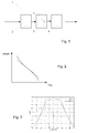
- a high-level diagram of a communication system 1 comprising receiver 2 for receiving signals, a signal processing arrangement 3 for processing signals and a transmitter 4 for transmitting signals.
- the system may be a satellite communication system.
- the processing arrangement 3 may comprise one or more filter network arrangements 5.
- the filter network arrangement may, for example, comprise a bandpass filter network and may, for example, be used in a demultiplexer for demultiplexing received signals into a number of frequency channels.
- the filter network arrangements may be used in an up- or down-converter. It should be realised that a filter network arrangement could alternatively be used for any other suitable purpose.
- the filter network arrangement is configured to let through signals of a specific frequency range and stop signals with frequencies outside the frequency range.
- the filter network arrangement will have some effect on the amplitude and the phase of the signals passed. For example, the loss of a real filter causes rounding of the passband amplitude and the amplitude selectivity of the filter causes a varying group delay.
- Group delay is a measure of how long it takes for a signal of a particular frequency to traverse a network.
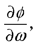
- the group delay is conventionally considered the derivative of the phase response of the network with respect to the angular frequency, ⁇ ⁇ ⁇ ⁇ , and, accordingly, the derivative of the phase response with respect to angular frequency will hereinafter be referred to as the "group delay".
- the dashed line of Figure 2 shows the relationship between the phase and the frequency for an ideal filter and the solid line of Figure 2 shows the relationship between the phase and the frequency for a real filter.
- the dashed line there is a linear relationship between the phase and the frequency for all signals that pass through an ideal filter network.
- the group delay for the passband of the filter network is the same irrespective of the frequency of the signal.
- a real filter will not have a constant group delay. Instead, the signals at the edges of the filter bandwidth will undergo a larger phase adjustment in a real filter than in an ideal filter, as indicated by the solid line of Figure 2 .
- the dashed line of Figure 3 shows the amplitude response of a lossless filter and the solid line of Figure 3 shows the amplitude response of a lossy filter.
- an n th order lossless filter will have n frequency points of perfect transmission, between which a small amount of power will be reflected.
- a lossy filter attenuates the amplitude significantly more than a lossless filter.
- the solid line of Figure 3 also shows rounding of the passbands for the lossy filter, caused by the finite quality factor (Q) of the filter. Loss is generally not a problem as long as it is uniform. Ideally, the gain across the passband should be constant.
- a filter network arrangement exhibits approximately uniform attenuation of signals across the frequencies in the passband. It will be shown that the filter network arrangement according to the invention will also have a flattened group delay. In reality, the gain and the group delay will not be exactly flat. An approximation to flatness in the form of a ripple function is considered acceptable. The key is that the gain and the group delay will be significantly flatter for the overall filter network arrangement than for the filter network on its own. In other words, the correction network improves the gain and group delay characteristics compared to the filter network on its own.
- the filter network arrangement 5 comprises a first port 6, a filter network 7, a coupler 8, two correction networks 9a, 9b and a second port 10.
- the correction networks 9a, 9b are provided to correct for the varying loss of the filter network 7 across the passband such that the signals passing through the filter network arrangement 5 are attenuated to approximately the same extent across the whole bandwidth of the filter.
- the correction networks also equalise the group delay. The two correction networks would effectively be identical.
- the filter network 7 of the filter network arrangement 5 may be a microwave filter.
- it could be a combline filter, interdigital filter or a waveguide filter.
- the filter network 7 is not limited to a microwave filter and it could be any frequency filter.
- the filter network 7 could be implemented in ceramics.
- it may be a low temperature co-fired (LTCC) ceramic filter.
- the coupler shown in Figure 4 is a 3dB coupler.
- the two correction networks 9a, 9b are both one-port correction networks. In the example of Figure 4 , a signal would be subject to the correction network whether it is passed from the first 6 to the second port 10 or the second port 10 to the first port 6.
- an appropriate correction network may be implemented by determining a correction network polynomial that will flatten the passband and synthesising the correction network from the polynomial. It is realised that if the correction network equalises the gain of the overall filter network arrangement it will also flatten the group delay, provided the Q of the correction network is close to the Q of the filter network 7. It is recognised, according to the invention, that the set of polynomials H(s) that give approximately flat group delay in the desired range includes polynomials that also flatten the gain.
- the group delay is equalised when the gain across the passband is equalised, provided that the respective Qs of the filter network and correction network have suitable values. It will then be shown how the relationship between the group delay and the loss can be used to design the correction network. Scattering parameters, also referred to as S-parameters, will be used to describe the electrical behaviour of the network.
- the filter and correction network are described in the lowpass domain. The units of angular frequency ⁇ are in radians/seconds, the units of the group delay are in seconds and the units of the gain are in decibles.
- H(s) is a Hurwitz stable polynomial representing the transfer function of the correction network
- ⁇ is angular frequency
- ⁇ k + i ⁇ k are the roots of H(s) and H(s) have K roots.
- f(s) of the correction network is controlled in order to compensate for the rounding of the passband of the filter network due to loss in the filter network. In words, additional loss is added to flatten the gain across the passband. Loss in a filter is generally not a problem as long as it is uniform.
- the filter network arrangement would typically be provided next to a low noise amplifier (LNA) and the extra loss in the filter network arrangement could be compensated for by increasing the LNA gain.
- LNA low noise amplifier
- adding loss corresponds to shifting the poles and zeros of the polynomial representing the transfer function to the left in the complex plane.
- making a network lossy is equivalent to adding a negative real part to the roots of the network polynomials.
- the bandwidth of the correction network is the same as the bandwidth of the filter network.
- ⁇ gd c is the gradient of the group delay with respect to - ⁇ (the real part of s)
- Equations 6 and 7 it can be seen from Equations 6 and 7 that the group delay of the correction network is affected very little by the addition of a small amount of loss.
- Some of the higher order terms in the Taylor series are non-zero and so gd c 1 is not exactly equal to gd c .
- S 11 l is S 11 of the lossy network and ⁇ ( S 11 S 11) is the gradient of S 11 S 11 with respect to - ⁇ and ⁇ 2 ( S 11 S 11) is the gradient of ⁇ ( S 11 S 11) with respect to - ⁇ , etc.
- Equation 9 shows that the loss of the correction network is a function of its group delay.
- the numerator polynomial has M roots and the denominator polynomial has P roots.
- r f - ⁇ m 1 M - ⁇ m 2 + ⁇ - ⁇ m 2 ⁇ m 2 + ⁇ - ⁇ m 2 2 .
- r f + O r f 3
- S 21 l is S 21 of the lossy filter network
- ⁇ ( S 21 S 21) is the gradient of S 21 S 21 with respect to - ⁇ .
- ⁇ ( S 21 S 21) -2. gd f .
- the gain of the filter network depends on the group delay.
- Equation 7 From Equation 7, it is known that gd c 1 ⁇ gd c and from Equation 15 it is known that gd f l ( ⁇ ) equals gd f ( ⁇ ) plus some extra higher order terms in the Taylor series. Consequently, from Equations 24 and 25 it can be seen that if the filter and correction network have the same or substantially the same Q, the conditions for a flat group delay and passband are the same and when the passband is flat the group delay is also flat and vice versa, provided that the extra terms in the Taylor series are small enough. In reality, the extra terms are small but still significant and so there has to be a slight trade off between the group delay equalisation and amplitude equalisation.
- the Q of the correction network is selected such that 1 ⁇ r c r f ⁇ 2.5 a satisfactorily uniform group delay may be obtained while, at the same time, the percentage of the bandwidth over which the passband is flattened is increased.
- the polynomial of the correction network is chosen to flatten the passband amplitude and the group delay for the selected Q factors. It will now be shown, with reference to Figure 5 , how an appropriate correction network polynomial that gives an approximately flat passband amplitude and group delay for the whole filter network arrangement can be found, according to the invention, and how a correction network can be synthesised based on the polynomial.
- the polynomial for the desired filter network is first determined (step S5.1). The skilled person would know how to determine a polynomial for a given filter network and the process will not be described in detail herein.
- the Q of the filter network is then chosen at step S5.2.
- the Q of the filter network depends on the type of resonators of the filter network and the medium in which they are implemented. Choosing the Q of the filter network may involve determining the technology to use and then determining the resulting Q. Alternatively, choosing the Q of the filter network may involve selecting a desired Q and then determining the technology to be used to provide the selected Q.
- An appropriate Q for the correction network is then determined based on the Q of the filter network (step 55.3). If the resonators of the correction network are selected to be of the same type as the resonators of the filter network and further selected to be implemented in the same medium, the Q of the correction network will be the same as the Q of the filter network.
- the Qs of the networks can also be chosen to be different. As will be described in more detail below, if the Qs of the correction network and the filter network are the same or substantially similar, the exact Q does not have to be known for the design and synthesis of the correction network and step S5.3 of choosing the Q of the correction network may involve choosing to make the Q of the correction network the same as the filter network.
- choosing the Q of the correction network may involve choosing to manufacture the correction network and the filter network in the same material and with the same type of resonators. If different Qs are instead used for the filter network and the correction network, step S5.3 may instead involve choosing a specific value for the Q for the correction network.
- the value of the Q for the correction network may be chosen to be sufficiently close to the value of Q for the filter network to provide a value of r c that complies with Equation 28 or at least Equation 27.
- a polynomial for representing the desired transfer function of the correction network then has to be determined.
- a Generalised Reverse Coefficient Bessel Polynomial may be used as the starting point for finding a suitable polynomial H(s) for the correction network.
- Equation 30 If a Bessel polynomial is used, it can be seen from Equation 30 that in the optimisation process to find the correction network polynomial, no matter what its order, there are only two variables, namely a, b.
- 2 F ( ⁇ n ( a,b ) ,Q ) , is a function of Q of the correction network and of ⁇ n , and therefore of a and b.
- the order of the correction network has a bearing on the degree of equalisation achievable.
- a correction network of order equal to that of the filter network is sufficient.
- a lower order network can be used with some compromise on the flatness of the gain and the group delay.
- a lower order correction network may be desirable in order to reduce the size of the overall filter network.
- step S 5 . 4 the coefficients of the polynomials need to be optimised.
- an error function is first constructed.
- S ⁇ 21 l ⁇ 2 where
- Equation 31 the group delay is flattened when the gain is flattened as long as the Q factors for the filter network and the correction network are the same and Equation 31 would then be the only error function that needs to be minimised to flatten both the gain and the group delay.
- the higher order terms in the Taylor expansion are in fact not zero and slightly different Q factors may be appropriate and it may therefore also be desired to consider an error function for minimising the group delay.
- gd c ⁇ ( ⁇ ) is the derivative of gd c ( ⁇ ) with respect to ⁇
- gd f l ⁇ ( ⁇ ) is the derivative of gd f l ( ⁇ ) with respect to ⁇ .
- the error function for the group delay can be found by differentiating expressions for group delay based on Equations 5 and 12 for a lossy network with respect to ⁇ and replacing the derivatives of the group delay in Equation 34 with the differentiated expressions.
- E ( ⁇ k, ⁇ k ) can be minimised for a number of points in the interval -1 ⁇ ⁇ ⁇ 1, using one or many appropriate optimisation techniques, to find the coefficients of the Generalized Reverse Coefficient Bessel Polynomial or other suitable polynomial chosen.
- Suitable values of a and b of the Generalised Reverse Coefficient Bessel Polynomial to minimise E 1 and/or a combination of E 1 and E 2 are determined using an appropriate optimisation technique.
- the error function may be minimised by an interactive process. It should be noted that, when the Qs are the same or substantially the same, the exact value of Q is not needed to find suitable values of a and b. A rough estimate of the Q is sufficient and the design will still be valid for a Q of, for example, half the design value. For a low Q filter, a fixed value of r c of 0.1 has been found suitable.
- the coefficients are optimised to provide a correction network in which all resonators have the same Q.
- a property of this symmetry is that when the network is synthesised there will be a constant resistive residue associated with each resonator.
- the polynomial has been described to be obtained from a Bessel polynomial as a starting point, it should be realised that other suitable polynomials can be used.
- the polynomial does not have to be a Bessel polynomial. If a Generalised Reverse Coefficient Bessel polynomial is used as a starting point, the final polynomial may not be a Bessel polynomial.
- the constraints that maintain the polynomial as a Bessel polynomial may be kept but in a second stage, when the error function is close to being minimised, the constraints are removed and the final polynomial for the correction network may therefore only be close to a Bessel polynomial.
- the determined polynomials for the filter network and the correction network can then be used to synthesise the filter network and the correction networks (step S5.5).
- An example of how to synthesise a correction network from the lossless H(s) is described below. However, it should be realised that a lossy H(s) could also be used. A constant resistive element would be extracted with each resonator.
- Equations 40 to 42 Equations 40 to 42 below.
- Capacitor C k and frequency invariant susceptance b k pairs are removed separated by unit admittance inverters, as is known in the art. Each stage reduces the order of the polynomials A(s) and C(s) by 1.
- correction network has been synthesised, various network transformations are carried out to arrive at a network approximation of the correction network in the form it would be manufactured as would be well known by the person skilled in the art.
- the correction network can then be manufactured. It will be appreciated that the correction network and the filter network would be manufactured using the technology determined to provide the Qs determined at steps S5.2 and S5.3. If a similar or the same Q factor is required in the filter network and the correction network, the correction network can be manufactured in the same or in a similar medium to the filter.
- a 4th order generalised Tchbeyshev filter with transmission zeros at -1.74i and 1.4i and poles (for a lossless filter) at -0.9640-0.6406i, -0.1589+1.1767i, -0.2419-1.2257i, -0.8810+0.7938i can be considered.
- the filter may be realised as a folded edge-coupled microstrip filter with centre frequency 1.345GHz and bandwidth 110MHz.
- a 2nd order correction network polynomial can be obtained.
- the poles of the obtained suitable lossless polynomial are determined to be at -0.8582+0.4615i and -0.8856-0.5245i.
- the zeros would be at 0.8582+0.4615i and 0.8856-0.5245i.
- the lossy poles and zeros would of course be shifted to the left in the complex plane by -r c .
- the one-port correction network may be synthesised from the polynomial using the method described above.
- the prototype network was then normalised, the shunt capacitors and frequency invariant susceptances were transformed to series half wavelength resonators and transformers were introduced into the inverters to scale the resonator admittance to unity, giving the network shown in Figure 6b .
- This network was then scaled to a 50 Ohm system and transformed to a coupled line microstrip circuit.
- the insertion loss and the group delay of the microstrip correction network obtained from an Agilent ADS circuit simulation are shown in Figures 7a and 7b respectively.
- the graph of Figure 7a shows the gain of the correction network, in decibels, across the passband and the graph of Figure 7b shows the group delay, in seconds, of the correction network across the passband.
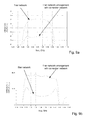
- Figure 9a shows the insertion loss of the final microstrip circuit compared to the insertion loss of the filter, obtained from an Agilent Momentum simulation.
- Figure 9b shows the group delay of the final microstrip circuit compared to the group delay of the filter, obtained from an Agilent Momentum simulation. The gain is shown in decibels and the group delay is shown in seconds in the graphs. It is clear that both the gain and the group delay of the filter network arrangement comprising the correction network is flatter than the gain and the group delay of the filter network on its own. It can be seen from Figure 9a that the variation in gain across the passband of the filter network arrangement is only approximately 30% of the variation in gain of the filter on its own.
- the filter network and the correction networks discussed with respect to Figures 6a, 6b, 7a , 7b, 8 , 9a and 9b are just one specific example and the correction network design technique, according to the invention, can be used to obtain a suitable correction network polynomial, and corresponding synthesised correction network, for compensating for the gain and group delay variation of any filter network.
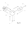
- FIG. 10 Another embodiment of the invention is shown in Figure 10 .
- the filter network arrangement 5 of Figure 10 comprises a first port 11, a circulator 12, an external correction network 9, a filter network 7, and a second port 13. Consequently, instead of the coupler, a circulator is used.
- the correction network 9 is identical to the correction networks 9a and 9b of Figure 4 , apart from that the correction network would have to be optimised to match the circulator instead of the couplers.
- the filter network may be a microwave filter.
- the filter network may be implemented in ceramics.
- the path taken by a signal received at the first port 11 is shown by solid arrows.
- a signal received at the first port 11 is passed by the circulator 12 to the one-port correction network 9 and from there to the filter network 7 to be filtered and output at the second port 13. Consequently, the external network 9 will correct the group delay and gain of a signal entering at the first port 11 and leaving at the second port 13.
- the path taken by a signal received at the second port 13 is shown by dashed arrows. Due to the nature of the circulator 12, a signal received at the second port 13 is passed directly from the filter network 7 to the first port 11, by-passing the correction network 9.
- a filter network as shown in Figure 4 may be provided as a multi-layer filter network arrangement. As a specific example, it may be a three layer LTCC structure with the filter network and the coupler on the middle layer and the correction networks on the top and bottom layer respectively.
- LTCC low temperature co-fired ceramic
- the correction network may be any suitable network. It may, for example, be a two-port network in which case no coupler or circulator would be needed.
- the described technique for synthesising the correction network would also be applicable for the two-port network.
- the polynomials discussed above give rise to a simple ladder one-port network.
- the equivalent two-port network would be more complex but could be used if appropriate for the application.
- the filter network and the correction network have been described to be connected by a coupler or a circulator, it should be realised that if the correction network allows, for example if the correction network is a two-port network, the correction network may be directly connected to the filter network.
- the correction network can be used with any type of suitable filter for which it is desired to equalise the group delay and gain.
- the filter network arrangement does not have to be used in a communication satellite.
Landscapes
- Engineering & Computer Science (AREA)
- Computer Networks & Wireless Communication (AREA)
- Signal Processing (AREA)
- Power Engineering (AREA)
- Aviation & Aerospace Engineering (AREA)
- General Physics & Mathematics (AREA)
- Physics & Mathematics (AREA)
- Astronomy & Astrophysics (AREA)
- Filters And Equalizers (AREA)
- Transmitters (AREA)
- Cable Transmission Systems, Equalization Of Radio And Reduction Of Echo (AREA)
- Image Processing (AREA)
- Networks Using Active Elements (AREA)
Abstract
Description
- The invention relates to filtering of signals. In particular, the invention relates to the equalising of attenuation and group delay across the passband of a filter network arrangement.
- Communication satellites typically process signals received and transmitted in a number of communication channels. To separate and combine the communication channels, the satellite may make use of a number of filters. Filters involved in signal processing are designed to meet often strict requirements on signal quality. Gain and group delay variation as a function of frequency can cause signal degradation. It is therefore desirable that filters involved in signal processing exhibit close to gain flatness and group delay flatness where possible.
- In non-minimum phase filters, cross-couplings within the filters have been used to equalise the group delay of the filters. This technique requires a higher order filter and there is a limit to the percentage of the bandwidth of the filter which can be corrected.
- It is also known to use external networks to equalise group delay across the passband of a filter. For example, external one-port networks have been used to add appropriate delays to signals in the passband.
- Moreover, it is known that the quality factor (Q) of the resonators of a filter can be adjusted in order to give some flattening of the passband. The Q of a resonator is a measure of the strength of the damping of its oscillations. To obtain a flat passband, very high Q filter resonators are conventionally used, which results in a filter with a relatively large size. To obtain a flat passband with lower Q resonators, pre-distortion, the introduction of complex transmission zeros or lossy cross couplings in the filter have been suggested. The use of complex zeros or lossy cross couplings to flatten the passband means that an increase in the complexity and the order of the filter is required.
- The invention aims to improve on the prior art.
- According to the invention, there is provided a filter network arrangement comprising a filter network; and one or more correction networks, wherein the one or more correction networks is configured to substantially equalise the passband gain and group delay of the filter network arrangement.
- It will be realised that the passband gain and group delay of the filter network arrangement will not be perfectly flat across the whole passband. However, the one or more external correction networks are arranged to reduce the variation in gain and group delay across the passband. The correction network is designed to have a gain and group delay that equalise the overall gain and the group delay to provide an approximately flat overall passband group delay and gain. By group delay, it is meant the derivative of the phase with respect to angular frequency.
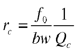
- The Qs of the filter network and the one or more correction network may be selected such that


- The Qs may be selected such that rc is greater than rf in order to achieve flattening of the passband for a greater percentage of the filter bandwidth for a given order of the one or more correction networks.
- Alternatively, the Q of the or each of the one or more correction networks can be chosen to be the same or substantially the same as the Q of the filter network. The filter network and the one or more correction network may be realised in the same or similar medium to ensure that the Q of the one or more correction networks is the same as the Q of the filter network.
- It has been found that if the one or more external correction networks has substantially the same Q as the filter network, there exist solutions for the one or more correction networks which will flatten the filter passband and also equalise the group delay of the filter network arrangement irrespective of the actual Q. Consequently, the precise Q of the filter network does not need to be known as long as the one or more correction network has substantially the same Q as the filter network, for example if the resonators of the one or more correction networks are of the same type and realised in the same or similar medium as the filter network. In other words, if the Q of the filter and the at least one correction network are the same a solution for the at least one correction network which flattens gain will also flatten group delay. The relationship is not exact so flattening of the gain will not give precise flattening of the group delay. A solution for the one or more correction networks may be selected which gives the best gain flatness, thereby providing a substantially flat group delay as well. In other words, a correction network that minimises the variation in gain of the filter network arrangement can be chosen and, as a consequence, the group delay variation would also be reduced.
- The invention allows a filter network with low Q resonators to be used and the size of the filter network can be reduced compared to filter networks that use high Q resonators to flatten the passband. Since an external network is added, the overall size of the filter network arrangement could of course be double the size of the filter network. However, the overall size would still be smaller or comparable to the filter network in which the passband of the filter was flattened by increasing the Q and, according to the invention, the group delay would also be equalised.
- The one or more correction networks may comprise one or more one-port networks and the filter network may comprise means for connecting the one or more one-port networks to the filter. At least one one-port correction network may be required depending on the arrangement of the circuit. In more detail, the means for connecting the one or more correction networks to the filter network may comprise a coupler or a circulator. If the connection means is a coupler, two one-port correction networks would be required.
- The order of the or each of the one or more correction network may be the same or lower than the order of the filter network to minimise the size of the network arrangement. Alternatively, the order of the correction network may be greater that the order of the filter network.
- The one or more correction networks may be synthesised from a polynomial H(s), the coefficients of which may be determined through optimising an error function for the gain and the group delay of the filter network arrangement. The roots of the polynomial may be optimised by minimising the error function for the gain on its own. The symmetry of the poles and zeros in the complex plane may be maintained about the line s=rc.
- The filter network arrangement may be a low temperature co-fired ceramic filter network arrangement. The filter network arrangement may be a multi-layer filter network arrangement.
- Alternatively, the filter network arrangement could be implemented as a microstrip.
- According to the invention, there is also provided a processing arrangement for a communication satellite comprising a filter network arrangement as set out above.
- Furthermore, according to the invention, there is provided a method of obtaining a filter network arrangement comprising a filter network and one or more correction networks for equalising the gain and the group delay across the passband of the filter network arrangement, the method comprising: determining a polynomial and a Q for a filter network; choosing a Q for the one or more correction networks; selecting a starting polynomial for the one or more correction networks and adjusting the coefficients of the polynomial to substantially equalise gain and group delay across the passband of the filter network; and synthesising the filter network and the one or more correction networks from the polynomial for the filter network and the polynomial for the one or more correction networks.
- The Q of the one or more correction networks may be selected based on the Q of the filter network. The Qs of the filter network and the one or more correction networks may be selected such that


- Adjusting the coefficients of the polynomial may comprise adjusting the coefficients of the polynomial in dependence of the Qs of the filter network and the correction networks. Determining the coefficients of the polynomial may comprise minimising the error function E(σ k, ω k ) = φE 1 (σ k , ωk) + γE 2 (σ k, ω k ), where φ, γ are weighting constants,

where
and
where σ k + iω k are the roots of the polynomial for the correction network, σ m + iω m are the roots of the numerator polynomial for the filter network and σ p + iω p are the roots of the denominator polynomial for the filter network. - When the Qs of the filter network and the one or more correction networks are the same, the precise values of rc and rf may be not required for the determination of the coefficients of the polynomial and only an estimate may be used.
- Minimising the error function may comprise first minimising E(σ k, ω k ) to find approximate coefficients for the correction network polynomial and then minimising E1 on its own to optimise the roots of the correction network polynomial.
- Finding the coefficients of the polynomial H(s) may comprise finding coefficients that minimise said error functions while still maintaining the symmetry of the correction network polynomial about the line s=rc,
- Embodiments of the invention will now be described, by way of example, with reference to
Figures 1 to 10 of the accompanying drawings, in which: -
Figure 1 is a schematic block diagram of a system in which a filter network arrangement is used; -
Figure 2 illustrates the phase variation with frequency of a real and an ideal filter network; -
Figure 3 illustrates the gain variation with frequency of a lossy and a lossless filter network; -
Figure 4 is a schematic diagram of a filter network arrangement according to a first embodiment of the invention; -
Figure 5 illustrates a method for designing a correction network according to an aspect of the invention; -
Figure 6a and 6b illustrate a prototype correction network and an example of a correction network at a later stage in the correction network synthesis process; -
Figure 7a and7b illustrate the loss and the group delay respectively of one example of a correction network; -
Figure 8 illustrates a microstrip layout for one example of a filter network arrangement; -
Figure 9a and Figure 9b illustrate the loss and group delay respectively of the complete circuit ofFigure 8 compared to the loss and group delay of the filter of the circuit on its own; and -
Figure 10 is a schematic diagram of a filter network arrangement according to a second embodiment of the invention. - With reference to
Figure 1 , a high-level diagram of acommunication system 1 is shown comprisingreceiver 2 for receiving signals, asignal processing arrangement 3 for processing signals and atransmitter 4 for transmitting signals. The system may be a satellite communication system. Theprocessing arrangement 3 may comprise one or morefilter network arrangements 5. The filter network arrangement may, for example, comprise a bandpass filter network and may, for example, be used in a demultiplexer for demultiplexing received signals into a number of frequency channels. Alternatively, the filter network arrangements may be used in an up- or down-converter. It should be realised that a filter network arrangement could alternatively be used for any other suitable purpose. - The filter network arrangement is configured to let through signals of a specific frequency range and stop signals with frequencies outside the frequency range. The filter network arrangement will have some effect on the amplitude and the phase of the signals passed. For example, the loss of a real filter causes rounding of the passband amplitude and the amplitude selectivity of the filter causes a varying group delay.
- Group delay is a measure of how long it takes for a signal of a particular frequency to traverse a network. The group delay is conventionally considered the derivative of the phase response of the network with respect to the angular frequency,
- The dashed line of
Figure 2 shows the relationship between the phase and the frequency for an ideal filter and the solid line ofFigure 2 shows the relationship between the phase and the frequency for a real filter. As indicated by the dashed line, there is a linear relationship between the phase and the frequency for all signals that pass through an ideal filter network. In other words, the group delay for the passband of the filter network is the same irrespective of the frequency of the signal. However, a real filter will not have a constant group delay. Instead, the signals at the edges of the filter bandwidth will undergo a larger phase adjustment in a real filter than in an ideal filter, as indicated by the solid line ofFigure 2 . - The dashed line of
Figure 3 shows the amplitude response of a lossless filter and the solid line ofFigure 3 shows the amplitude response of a lossy filter. For equi-ripple filter functions, an nth order lossless filter will have n frequency points of perfect transmission, between which a small amount of power will be reflected. As shown inFigure 3 , a lossy filter attenuates the amplitude significantly more than a lossless filter. The solid line ofFigure 3 also shows rounding of the passbands for the lossy filter, caused by the finite quality factor (Q) of the filter. Loss is generally not a problem as long as it is uniform. Ideally, the gain across the passband should be constant. - A filter network arrangement according to embodiments of the invention exhibits approximately uniform attenuation of signals across the frequencies in the passband. It will be shown that the filter network arrangement according to the invention will also have a flattened group delay. In reality, the gain and the group delay will not be exactly flat. An approximation to flatness in the form of a ripple function is considered acceptable. The key is that the gain and the group delay will be significantly flatter for the overall filter network arrangement than for the filter network on its own. In other words, the correction network improves the gain and group delay characteristics compared to the filter network on its own.
- With reference to
Figure 4 , one embodiment of a filter network arrangement according to the invention is shown. Thefilter network arrangement 5 comprises afirst port 6, afilter network 7, acoupler 8, twocorrection networks second port 10. Thecorrection networks filter network 7 across the passband such that the signals passing through thefilter network arrangement 5 are attenuated to approximately the same extent across the whole bandwidth of the filter. The correction networks also equalise the group delay. The two correction networks would effectively be identical. - The
filter network 7 of thefilter network arrangement 5 may be a microwave filter. For example, it could be a combline filter, interdigital filter or a waveguide filter. However, it will be realised that thefilter network 7 is not limited to a microwave filter and it could be any frequency filter. Thefilter network 7 could be implemented in ceramics. For example, it may be a low temperature co-fired (LTCC) ceramic filter. The coupler shown inFigure 4 is a 3dB coupler. According to some embodiments of the invention, the twocorrection networks Figure 4 , a signal would be subject to the correction network whether it is passed from the first 6 to thesecond port 10 or thesecond port 10 to thefirst port 6. - According to some embodiments of the invention, given the transfer function of the
filter network 7, an appropriate correction network may be implemented by determining a correction network polynomial that will flatten the passband and synthesising the correction network from the polynomial. It is realised that if the correction network equalises the gain of the overall filter network arrangement it will also flatten the group delay, provided the Q of the correction network is close to the Q of thefilter network 7. It is recognised, according to the invention, that the set of polynomials H(s) that give approximately flat group delay in the desired range includes polynomials that also flatten the gain. It is realised that as long as the correction network and the filter network have similar Qs, by selecting a polynomial that flattens the gain of the passband the group delay is also flattened. However, if the Qs are different, an appropriate correction network polynomial can still be found that substantially equalises both the gain and the group delay of the filter network arrangement. In other words, a correction network can be synthesised that simultaneously corrects both the group delay and the gain of the filter network arrangement. As will be described in more detail below, in the design of the filter network arrangement, the focus is on flattening the gain and the flattening of the group delay then follows. - It will now be shown mathematically that the group delay is equalised when the gain across the passband is equalised, provided that the respective Qs of the filter network and correction network have suitable values. It will then be shown how the relationship between the group delay and the loss can be used to design the correction network. Scattering parameters, also referred to as S-parameters, will be used to describe the electrical behaviour of the network. In the discussion below, the filter and correction network are described in the lowpass domain. The units of angular frequency ω are in radians/seconds, the units of the group delay are in seconds and the units of the gain are in decibles.
- S11 of a lossless correction network can be written as

where H(s) is a Hurwitz stable polynomial representing the transfer function of the correction network, ω is angular frequency, σ k + iω k are the roots of H(s) and H(s) have K roots. - For a lossless purely reactive one-port network, there is symmetry of the poles and zeros of S11 around ω = 0 and the gain of the correction network can be written as

whereS11 is the complex conjugate of S11. - If we add some loss to the correction network we break the unity condition and

where f(s) < 1. According to embodiments of the invention, f(s) of the correction network is controlled in order to compensate for the rounding of the passband of the filter network due to loss in the filter network. In words, additional loss is added to flatten the gain across the passband. Loss in a filter is generally not a problem as long as it is uniform. The filter network arrangement would typically be provided next to a low noise amplifier (LNA) and the extra loss in the filter network arrangement could be compensated for by increasing the LNA gain. - Mathematically, adding loss corresponds to shifting the poles and zeros of the polynomial representing the transfer function to the left in the complex plane. Put a different way, making a network lossy is equivalent to adding a negative real part to the roots of the network polynomials. The poles and zeros are shifted to the left in the complex plane by shifting the real part σ k by a constant amount rc, where rc is related to the Qc of the resonators used in the final realisation of the correction network as shown below:

where fo is the centre frequency and bw the bandwidth of the correction network. The bandwidth of the correction network is the same as the bandwidth of the filter network. The symmetry of S11 is maintained for a lossy network but the line of symmetry is shifted to s = r c. - The group delay of a correction network can be written as

- The Taylor series for the group delay and the insertion loss with respect to - σ (the real part of s) can be examined to see the effect of adding loss to lossless networks. As will be shown below, a relationship between the group delay and the insertion loss which is considered when designing the filter network arrangement according to the invention can then be found.
- The Taylor expansion of the group delay is

where ∇gdc is the gradient of the group delay with respect to - σ (the real part of s), and gdc1 is the group delay of the lossy correction network. Due to the symmetry of the poles and zeros of S11 of the lossless, purely reactive correction network, ∇gdc = 0 and thus
provided that the higher order terms in the Taylor expansion are small. - Consequently, it can be seen from
Equations 1 is not exactly equal to gdc. - The Taylor expansion of the gain of
Equation 2 gives
where S11 l is S11 of the lossy network and ∇(S11 S11) is the gradient ofS11 S11 with respect to - σ and ∇2(S11 S11) is the gradient of ∇(S11 S11) with respect to -σ, etc. It can be found that
S11 S11) = -2.S11 S11.gdc. It can further be found that ∇2(S11 S11) = 4S11 S11.gdc 2 + 2S11 S11.∇gdc. Considering that ∇gdc = 0, it can be seen that
S11 S11=1, it follows that

-
Equation 9 shows that the loss of the correction network is a function of its group delay. - A similar analysis can be carried out for a filter network. S21 for a lossless filter network can be written as

where ω is angular frequency, σ m + iω m are the roots of the numerator polynomial and σ p + iω p are the roots of the denominator polynomial for the filter network. The numerator polynomial has M roots and the denominator polynomial has P roots. - Consequently, the gain of the filter network can be written as

and the group delay of the filter network can be written as
- To take into account the loss and therefore the finite Q of the filter resonators (Qf), the poles and zeros of the filter transfer function must be shifted to the left in the complex plane by a constant amount rf, where rf is related to Qf by

where fo is the centre frequency and bw the bandwidth of thefilter network 7. - As before, the Taylor series for the group delay and the insertion loss with respect to - σ (the real part) can be examined to see the effect of adding loss to the lossless filter networks. The Taylor series expansion of the group delay becomes

where ∇gdf is the gradient of the group delay with respect to -σ, and gdfl is the group delay of the lossy filter network. For the filter network, there is no symmetry for the poles and zeros and so ∇gdf ≠ 0. - If
Equation 14 is expanded, it becomes
- For a small change rf in σ p and σ m, the gain of the filter network becomes

where S21 l is S21 of the lossy filter network and ∇(S21 S21) is the gradient ofS21 S21 with respect to -σ. Now ∇(S21 S21)=-2.gdf .S21 S21 and thus
where ∇(S21 S21.gf ) is the gradient ofS21 S21.gdf with respect to -σ, etc. - This time, since ∇dgf ≠ 0, there will be terms ∇dgf, ∇2 dgf etc. However, by expanding Equation 17 it can be seen that the dominant terms can be written as
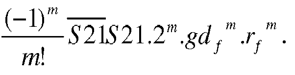

S21 lS21 l ≈S21 S21.exp(-2.gdf.rf ), which is the same as
- Again, it can be seen that the gain of the filter network depends on the group delay.
- Cascading the correction network and the filter network it is found from
Equations 9 and 18 that the combined gain for the corrected network and the filter network is
- For perfect group delay equalisation we require:

where C is a constant. - For perfect gain we also require
Equation 19 to be equal to a constant. It can be seen fromEquation 19 that the passband is perfectly flat when
and K is a constant. - If the filter network and the correction network have very similar or the same Qs, rc=rf and Equation 21 can be rewritten as follows:

- For different Qs, we write

- In practice, the gain and group delay will not be exactly flat and it is acceptable if the gain and group delay across the passband is a ripple function. Consequently,
equations 20, 22 and 23 can be written as


where f(ω), g(ω) and h(ω) are ripple functions. It is of course desired that the ripples are small to minimise the variation in gain and group delay and provide a gain and a group delay that is approximately uniform across the passband. - From
Equation 7, it is known that gdc1 ≈ gdc and fromEquation 15 it is known that gdfl (ω) equals gdf (ω) plus some extra higher order terms in the Taylor series. Consequently, from Equations 24 and 25 it can be seen that if the filter and correction network have the same or substantially the same Q, the conditions for a flat group delay and passband are the same and when the passband is flat the group delay is also flat and vice versa, provided that the extra terms in the Taylor series are small enough. In reality, the extra terms are small but still significant and so there has to be a slight trade off between the group delay equalisation and amplitude equalisation. - If the filter network and the correction network have very similar but not exactly the same Qs, an acceptable approximation to group delay and gain flatness is still provided if the group delay of the filter network and the correction network exhibit the relationship of Equation 25.
- Moreover, it has been found, that if the Qs are different, a polynomial for the correction network can still be found that satisfies both Equations 24 and 26. In more detail, it has been found that as long as

the group delay is approximately flat when the amplitude is approximately flat. In fact, it has been found that using a slightly lower Q for the correction network than for the filter network allows flattening of the passband for a greater percentage of the filter bandwidth for a given order of correction network. In other words, when extra loss is added to the correction network to give an rc that is higher than rf, a greater percentage of the filter passband can be flattened for a given order of correction network. As a specific example, it has been found that a Q for the correction network that gives rc=2rf is suitable for increasing the bandwidth over which the passband is flattened but also providing a substantially uniform group delay. In fact, as long as the Q of the correction network is selected such that
- According to embodiments of the invention, the polynomial of the correction network is chosen to flatten the passband amplitude and the group delay for the selected Q factors. It will now be shown, with reference to
Figure 5 , how an appropriate correction network polynomial that gives an approximately flat passband amplitude and group delay for the whole filter network arrangement can be found, according to the invention, and how a correction network can be synthesised based on the polynomial. - The polynomial for the desired filter network is first determined (step S5.1). The skilled person would know how to determine a polynomial for a given filter network and the process will not be described in detail herein. The Q of the filter network is then chosen at step S5.2. The Q of the filter network depends on the type of resonators of the filter network and the medium in which they are implemented. Choosing the Q of the filter network may involve determining the technology to use and then determining the resulting Q. Alternatively, choosing the Q of the filter network may involve selecting a desired Q and then determining the technology to be used to provide the selected Q.
- An appropriate Q for the correction network is then determined based on the Q of the filter network (step 55.3). If the resonators of the correction network are selected to be of the same type as the resonators of the filter network and further selected to be implemented in the same medium, the Q of the correction network will be the same as the Q of the filter network. The Qs of the networks can also be chosen to be different. As will be described in more detail below, if the Qs of the correction network and the filter network are the same or substantially similar, the exact Q does not have to be known for the design and synthesis of the correction network and step S5.3 of choosing the Q of the correction network may involve choosing to make the Q of the correction network the same as the filter network. For example, choosing the Q of the correction network may involve choosing to manufacture the correction network and the filter network in the same material and with the same type of resonators. If different Qs are instead used for the filter network and the correction network, step S5.3 may instead involve choosing a specific value for the Q for the correction network. The value of the Q for the correction network may be chosen to be sufficiently close to the value of Q for the filter network to provide a value of rc that complies with Equation 28 or at least Equation 27.
- A polynomial for representing the desired transfer function of the correction network then has to be determined. For example, a Generalised Reverse Coefficient Bessel Polynomial may be used as the starting point for finding a suitable polynomial H(s) for the correction network. The Generalised Reverse Coefficient Bessel Polynomial is a solution to the 2nd order differential equation:

where a and b are complex values and n is a positive integer. - The solutions to Equation 29 are of the form:

where
- If a Bessel polynomial is used, it can be seen from
Equation 30 that in the optimisation process to find the correction network polynomial, no matter what its order, there are only two variables, namely a, b. The insertion loss of the correction network, |S11 l |2 = F(θ n (a,b),Q), is a function of Q of the correction network and of θn , and therefore of a and b. - Of course the order of the correction network has a bearing on the degree of equalisation achievable. Generally, a correction network of order equal to that of the filter network is sufficient. However a lower order network can be used with some compromise on the flatness of the gain and the group delay. A lower order correction network may be desirable in order to reduce the size of the overall filter network.
- Once a suitable polynomial as a starting point for the correction network has been chosen, the coefficients of the polynomials need to be optimised (step S5.4). To find the coefficients of the final polynomial, an error function is first constructed.
- A suitable error function for minimising the gain is given by

where
where σ k + iω k are the roots of the polynomial for the correction network, σ m + iω m are the roots of the numerator polynomial for the filter network and σ p + iω p, are the roots of the denominator polynomial for the filter network. - From
Equations l (ω) equals gdf (ω) inEquation 15, it is realised that the group delay is flattened when the gain is flattened as long as the Q factors for the filter network and the correction network are the same and Equation 31 would then be the only error function that needs to be minimised to flatten both the gain and the group delay. However, the higher order terms in the Taylor expansion are in fact not zero and slightly different Q factors may be appropriate and it may therefore also be desired to consider an error function for minimising the group delay. - A suitable error function for minimising the group delay is given by

- It should be noted that the error function for the group delay is found by first differentiating
Equation 20 with respect to ω, which gives
where

l (ω) with respect to ω. In reality, the sum of the derivatives of the group delays of the correction network and the filter network will not be exactly zero but should be minimised to flatten the overall group delay of the filter network arrangement. The error function for the group delay can be found by differentiating expressions for group delay based onEquations - Equations 31 and 33 can be combined to give a combined error function:

where φ,γ are weighting constants defining the importance of group delay or amplitude flatness. E(σk, ω k ) can be minimised for a number of points in the interval -1 ≤ ω ≤ 1, using one or many appropriate optimisation techniques, to find the coefficients of the Generalized Reverse Coefficient Bessel Polynomial or other suitable polynomial chosen. - The relationships between the group delay and the gain shown above are not exact and it is has been found that sometimes it is better to flatten the amplitude and accept the group delay that follows. In other words, a polynomial may be chosen that only minimises the error function for the gain E1. Having a nearly perfectly flat passband is sometimes more important than having a perfectly constant group delay. In some embodiments, the determination of the coefficients of the correction network polynomial can be considered to be carried out in two parts. First, equation 35 is minimised to find approximate coefficients. The roots of the correction polynomial are then optimised by minimising E1 from Equation 31 only. For example, it is contemplated that when the Qs are the same or substantially the same, only the error function for the gain is minimised to find the coefficients of the polynomial since when the Qs are the same or similar the group delay is substantially flat when the gain is substantially flat. Only minimising the error function for the gain E1 can be considered to correspond to minimising the error function E of Equation 35 but with a zero value assigned to the weighting coefficient γ for E2. Moreover, it is contemplated that when the Qs are different, both the error functions for the gain and the group delay are minimised to find the coefficients of the polynomial. Values may be selected for the weighting constants of Equation 35 that give more weight to either the error function for the gain or the error function for the group delay. Of course, both error functions may be considered even when the Qs are the same or similar.
- Suitable values of a and b of the Generalised Reverse Coefficient Bessel Polynomial to minimise E1 and/or a combination of E1 and E2 are determined using an appropriate optimisation technique. The error function may be minimised by an interactive process. It should be noted that, when the Qs are the same or substantially the same, the exact value of Q is not needed to find suitable values of a and b. A rough estimate of the Q is sufficient and the design will still be valid for a Q of, for example, half the design value. For a low Q filter, a fixed value of rc of 0.1 has been found suitable.
- If different Qs are used, the bandwidth over which both the passband and the group delay are flat could be slightly increased. However, the precise values of Qs for both networks are then needed for the optimisation.
- Accordingly, when the Qs are the same or substantially the same an estimate of rc and rf would be used in the error functions E1 and E2. When the Qs are different, more precise values of rc and rf would instead be used in the error functions E1 and E2.
- When finding the coefficients of the polynomial to minimise the error function, the symmetry of the correction network polynomial is maintained about the line s=rc. In other words, the coefficients are optimised to provide a correction network in which all resonators have the same Q. A property of this symmetry is that when the network is synthesised there will be a constant resistive residue associated with each resonator.
- It will be appreciated that although one specific example of a gain error function and a group delay error function has been given above, alternative error functions can be constructed and the optimisation of the correction network is not limited to the use of the error functions described herein.
- Moreover, although the polynomial has been described to be obtained from a Bessel polynomial as a starting point, it should be realised that other suitable polynomials can be used. The polynomial does not have to be a Bessel polynomial. If a Generalised Reverse Coefficient Bessel polynomial is used as a starting point, the final polynomial may not be a Bessel polynomial. In a first stage of the minimisation of the error function, the constraints that maintain the polynomial as a Bessel polynomial may be kept but in a second stage, when the error function is close to being minimised, the constraints are removed and the final polynomial for the correction network may therefore only be close to a Bessel polynomial.
- The determined polynomials for the filter network and the correction network can then be used to synthesise the filter network and the correction networks (step S5.5). An example of how to synthesise a correction network from the lossless H(s) is described below. However, it should be realised that a lossy H(s) could also be used. A constant resistive element would be extracted with each resonator.
- To start the network synthesis process, it can be considered that the admittance Y(s) for the one-port network is given by

- Equation 36 can be rewritten as

where Ho(s) is the odd part of H(s) and He(s) is the even part of H(s). - For the special case of pole-zero complex conjugate symmetry this reduces to

- The synthesis of the one-port network can be performed by removing elements from the admittance function of Equations 37 or 38. When H(s) has complex conjugate symmetry, elements can be extracted from Equation 38 by continued fraction expansion. However, for the general case, H(s) has complex coefficients and elements must be extracted from the admittance function of Equation 37. It is then useful to consider that Equation 37 can be written as

where A(s) and C(s) are chain matrix parameters. - Shunt capacitors and frequency invariant susceptances followed by unit inverters can then repeatedly be extracted by multiplying the chain matrix from the polynomials by that of the negative of the element to be extracted, to give a network with the topology of
Figure 6a , as will be described in more detail below. Equations for removing elements are provided asEquations 40 to 42 below. - For the removal of a capacitor Ck, the following equation can be used.

where
- For the removal of a frequency invariant susceptance bk, the following equation can be used.


- For the removal of a unit admittance inverter, the following equation can be used

- Capacitor Ck and frequency invariant susceptance bk pairs are removed separated by unit admittance inverters, as is known in the art. Each stage reduces the order of the polynomials A(s) and C(s) by 1.
- Once the correction network has been synthesised, various network transformations are carried out to arrive at a network approximation of the correction network in the form it would be manufactured as would be well known by the person skilled in the art. The correction network can then be manufactured. It will be appreciated that the correction network and the filter network would be manufactured using the technology determined to provide the Qs determined at steps S5.2 and S5.3. If a similar or the same Q factor is required in the filter network and the correction network, the correction network can be manufactured in the same or in a similar medium to the filter.
- An example of finding a suitable correction network for a specific filter and of incorporating the correction network into a filter network arrangement will now be described. As an example, a 4th order generalised Tchbeyshev filter with transmission zeros at -1.74i and 1.4i and poles (for a lossless filter) at -0.9640-0.6406i, -0.1589+1.1767i, -0.2419-1.2257i, -0.8810+0.7938i can be considered. The Q of the filter is approximately 100 with rf=0.12.
- The filter may be realised as a folded edge-coupled microstrip filter with centre frequency 1.345GHz and bandwidth 110MHz. A substrate with a relative permittivity ξr of 9.8, and a thickness 0.635mm was considered.
- Using the above described method for finding the coefficients of the correction network polynomial, a 2nd order correction network polynomial can be obtained. The Q of the correction network is also chosen to be approximately 100 with rc=0.12. The poles of the obtained suitable lossless polynomial are determined to be at -0.8582+0.4615i and -0.8856-0.5245i. The zeros would be at 0.8582+0.4615i and 0.8856-0.5245i. The lossy poles and zeros would of course be shifted to the left in the complex plane by -rc.
- The one-port correction network may be synthesised from the polynomial using the method described above. A prototype one-port network as shown in
Figure 6a was obtained, with values C1=0.5734, b1=0.0225, C2=1.7385 and b2=0.0413. The prototype network was then normalised, the shunt capacitors and frequency invariant susceptances were transformed to series half wavelength resonators and transformers were introduced into the inverters to scale the resonator admittance to unity, giving the network shown inFigure 6b . - For the network shown in
Figure 6b ,
- This network was then scaled to a 50 Ohm system and transformed to a coupled line microstrip circuit. The insertion loss and the group delay of the microstrip correction network obtained from an Agilent ADS circuit simulation are shown in
Figures 7a and7b respectively. The graph ofFigure 7a shows the gain of the correction network, in decibels, across the passband and the graph ofFigure 7b shows the group delay, in seconds, of the correction network across the passband. - Two copies of the correction network were incorporated with a branch line coupler and the microstrip filter was added to this circuit to give a final circuit as shown in
Figure 8 . Thefilter network 7, thecoupler 8 and thecorrection networks Figure 8 . -
Figure 9a shows the insertion loss of the final microstrip circuit compared to the insertion loss of the filter, obtained from an Agilent Momentum simulation.Figure 9b shows the group delay of the final microstrip circuit compared to the group delay of the filter, obtained from an Agilent Momentum simulation. The gain is shown in decibels and the group delay is shown in seconds in the graphs. It is clear that both the gain and the group delay of the filter network arrangement comprising the correction network is flatter than the gain and the group delay of the filter network on its own. It can be seen fromFigure 9a that the variation in gain across the passband of the filter network arrangement is only approximately 30% of the variation in gain of the filter on its own. Correspondingly, it can be seen fromFigure 9b that the variation in group delay of the filter network arrangement is only approximately 40% of the variation in group delay of the filter on its own. The variation in gain and group delay can be reduced further by increasing the order of the correction networks. Consequently, the example ofFigures 6a, 6b, 7a ,7b, 8 ,9a and 9b show that a correction network can be provided, according to the invention, that flattens the attenuation and the group delay of a filter across the passband of the filter. Accordingly, the invention provides a filter network arrangement with improved group delay and gain characteristics compared to the filter network on its own. - It should be realised that the filter network and the correction networks discussed with respect to
Figures 6a, 6b, 7a ,7b, 8 ,9a and 9b are just one specific example and the correction network design technique, according to the invention, can be used to obtain a suitable correction network polynomial, and corresponding synthesised correction network, for compensating for the gain and group delay variation of any filter network. - Another embodiment of the invention is shown in
Figure 10 . Like reference numerals indicate like components. Thefilter network arrangement 5 ofFigure 10 comprises afirst port 11, acirculator 12, anexternal correction network 9, afilter network 7, and asecond port 13. Consequently, instead of the coupler, a circulator is used. Thecorrection network 9 is identical to thecorrection networks Figure 4 , apart from that the correction network would have to be optimised to match the circulator instead of the couplers. As before, the filter network may be a microwave filter. The filter network may be implemented in ceramics. The path taken by a signal received at thefirst port 11 is shown by solid arrows. A signal received at thefirst port 11 is passed by thecirculator 12 to the one-port correction network 9 and from there to thefilter network 7 to be filtered and output at thesecond port 13. Consequently, theexternal network 9 will correct the group delay and gain of a signal entering at thefirst port 11 and leaving at thesecond port 13. The path taken by a signal received at thesecond port 13 is shown by dashed arrows. Due to the nature of thecirculator 12, a signal received at thesecond port 13 is passed directly from thefilter network 7 to thefirst port 11, by-passing thecorrection network 9. - Since a circulator is used instead of a coupler in the embodiment of
Figure 10 , only a single correction network is required instead of two correction networks as shown inFigure 4 . However, for some frequencies 3dB couplers can be made much smaller than circulators and consequently the filter network arrangement ofFigure 10 could be bigger and heavier than the filter network arrangement ofFigure 4 . - It is contemplated that the filter network arrangements of
Figure 4 and10 may be implemented as low temperature co-fired ceramic (LTCC) filter network arrangements. To provide a small and compact structure, a filter network as shown inFigure 4 may be provided as a multi-layer filter network arrangement. As a specific example, it may be a three layer LTCC structure with the filter network and the coupler on the middle layer and the correction networks on the top and bottom layer respectively. - Whilst specific examples of the invention have been described, the scope of the invention is defined by the appended claims and not limited to the examples. The invention could therefore be implemented in other ways, as would be appreciated by those skilled in the art.
- For example, it should also be realised that although the correction network has been described in the two embodiments above as a one-port network, the correction network may be any suitable network. It may, for example, be a two-port network in which case no coupler or circulator would be needed. The described technique for synthesising the correction network would also be applicable for the two-port network. The polynomials discussed above give rise to a simple ladder one-port network. The equivalent two-port network would be more complex but could be used if appropriate for the application.
- Moreover, although the filter network and the correction network have been described to be connected by a coupler or a circulator, it should be realised that if the correction network allows, for example if the correction network is a two-port network, the correction network may be directly connected to the filter network.
- It should also be understood that although the embodiments have been described with respect to a microstrip or an LTCC network, any type of suitable integrated circuit can be used.
- Additionally, it should be realised that the correction network can be used with any type of suitable filter for which it is desired to equalise the group delay and gain. The filter network arrangement does not have to be used in a communication satellite.
Claims (15)
- A filter network arrangement comprising:a filter network; andone or more correction networks, wherein the one or more correction networks is arranged to substantially equalise the passband gain and group delay of the filter network arrangement and wherein group delay is the derivative of phase with respect to angular frequency.
- A filter network according to claim 1, wherein the Qs of the filter network and the one or more correction networks are selected such that


- A filter network according to claim 2, wherein rc is greater than rf.
- A filter network according to claim 1 or 2, wherein the one or more correction networks has the same or substantially the same Q as the filter network.
- A filter network according to claim 4, wherein the filter network and the one or more correction networks are implemented in the same or similar medium.
- A filter network arrangement according to any one of the preceding claims, wherein the one or more correction networks comprises one or more one-port networks.
- A filter network arrangement according to claim 6, wherein the one or more correction networks comprise two identical correction networks and the filter network arrangement comprises a coupler for connecting the correction networks and the filter network.
- A filter network arrangement according to claim 6, wherein the one or more correction networks comprises a single correction network and the filter network arrangement comprises a circulator for connecting the correction network to the filter network.
- A filter network arrangement according to any one of the preceding claims, wherein the order of the one or more correction networks is the same or lower than the order of the filter network.
- A low temperature co-fired ceramic (LTCC) structure comprising a filter network arrangement according to any one of the preceding claims.
- A processing arrangement for a communication satellite comprising a filter network arrangement according to any one of claims 1 to 9 or a LTCC structure according to claim 10.
- A method of obtaining a filter network arrangement comprising a filter network and one or more correction networks for equalising the gain and the group delay across the passband of the filter network arrangement, the method comprising:determining a polynomial and Q for a filter network;choosing a Q for the one or more correction networks;selecting a starting polynomial for the one or more correction networks and adjusting the coefficients of the polynomial to substantially equalise gain and group delay across the passband of the filter network; andsynthesising the filter network and the one or more correction networks from the polynomial for the filter network and the polynomial for the one or more correction networks.
- A method according to claim 12, wherein the Qs of the filter network and the one or more correction networks are selected such that


- A method according to claim 12 or 13, wherein determining the coefficients of the polynomial comprises minimising the error function E(σ k , ω k ) = φE 1(σ k, ω k ) + γE 2(σk , ω k ) where φ,γ are weighting constants,


where σ k + iω k are the roots of the polynomial for the correction network, σm + iω m are the roots of the numerator polynomial for the filter network and σ p + iω p are the roots of the denominator polynomial for the filter network. - A method according to claim 14, wherein minimising the error function comprises first minimising E(σk, ω k ) to find approximate coefficients for the correction network polynomial and then minimising E1 on its own to optimise the roots of the correction network polynomial.
Priority Applications (8)
| Application Number | Priority Date | Filing Date | Title |
|---|---|---|---|
| DK12275064T DK2663042T3 (en) | 2012-05-09 | 2012-05-09 | Filter Network Event |
| EP20120275064 EP2663042B1 (en) | 2012-05-09 | 2012-05-09 | A Filter Network Arrangement |
| ES12275064.9T ES2503690T3 (en) | 2012-05-09 | 2012-05-09 | Filter network layout |
| CA 2872544 CA2872544A1 (en) | 2012-05-09 | 2013-05-03 | A filter network arrangement |
| AU2013258226A AU2013258226B2 (en) | 2012-05-09 | 2013-05-03 | A filter network arrangement |
| PCT/EP2013/059311 WO2013167498A1 (en) | 2012-05-09 | 2013-05-03 | A filter network arrangement |
| US14/399,810 US9237042B2 (en) | 2012-05-09 | 2013-05-03 | Filter network arrangement |
| IN10036DEN2014 IN2014DN10036A (en) | 2012-05-09 | 2014-11-26 |
Applications Claiming Priority (1)
| Application Number | Priority Date | Filing Date | Title |
|---|---|---|---|
| EP20120275064 EP2663042B1 (en) | 2012-05-09 | 2012-05-09 | A Filter Network Arrangement |
Publications (2)
| Publication Number | Publication Date |
|---|---|
| EP2663042A1 true EP2663042A1 (en) | 2013-11-13 |
| EP2663042B1 EP2663042B1 (en) | 2014-08-27 |
Family
ID=48289202
Family Applications (1)
| Application Number | Title | Priority Date | Filing Date |
|---|---|---|---|
| EP20120275064 Not-in-force EP2663042B1 (en) | 2012-05-09 | 2012-05-09 | A Filter Network Arrangement |
Country Status (8)
| Country | Link |
|---|---|
| US (1) | US9237042B2 (en) |
| EP (1) | EP2663042B1 (en) |
| AU (1) | AU2013258226B2 (en) |
| CA (1) | CA2872544A1 (en) |
| DK (1) | DK2663042T3 (en) |
| ES (1) | ES2503690T3 (en) |
| IN (1) | IN2014DN10036A (en) |
| WO (1) | WO2013167498A1 (en) |
Families Citing this family (3)
| Publication number | Priority date | Publication date | Assignee | Title |
|---|---|---|---|---|
| US11277384B2 (en) * | 2018-12-11 | 2022-03-15 | Level 3 Communications, Llc | Dynamic filter generation and distribution within computer networks |
| CN113630145B (en) * | 2021-08-25 | 2024-12-31 | 广东圣大电子有限公司 | A flat group delay radio frequency transceiver |
| CN114818580B (en) * | 2022-06-27 | 2022-10-18 | 华南理工大学 | Method and system for extracting equivalent circuit of filter device and method and system for reconstructing parameters |
Citations (1)
| Publication number | Priority date | Publication date | Assignee | Title |
|---|---|---|---|---|
| WO2010097349A2 (en) * | 2009-02-27 | 2010-09-02 | Astrium Limited | Compensation apparatus |
-
2012
- 2012-05-09 EP EP20120275064 patent/EP2663042B1/en not_active Not-in-force
- 2012-05-09 ES ES12275064.9T patent/ES2503690T3/en active Active
- 2012-05-09 DK DK12275064T patent/DK2663042T3/en active
-
2013
- 2013-05-03 WO PCT/EP2013/059311 patent/WO2013167498A1/en not_active Ceased
- 2013-05-03 US US14/399,810 patent/US9237042B2/en not_active Expired - Fee Related
- 2013-05-03 CA CA 2872544 patent/CA2872544A1/en not_active Abandoned
- 2013-05-03 AU AU2013258226A patent/AU2013258226B2/en not_active Ceased
-
2014
- 2014-11-26 IN IN10036DEN2014 patent/IN2014DN10036A/en unknown
Patent Citations (1)
| Publication number | Priority date | Publication date | Assignee | Title |
|---|---|---|---|---|
| WO2010097349A2 (en) * | 2009-02-27 | 2010-09-02 | Astrium Limited | Compensation apparatus |
Also Published As
| Publication number | Publication date |
|---|---|
| DK2663042T3 (en) | 2014-10-06 |
| AU2013258226A1 (en) | 2014-11-27 |
| US9237042B2 (en) | 2016-01-12 |
| AU2013258226B2 (en) | 2016-01-07 |
| ES2503690T3 (en) | 2014-10-07 |
| US20150124857A1 (en) | 2015-05-07 |
| WO2013167498A1 (en) | 2013-11-14 |
| CA2872544A1 (en) | 2013-11-14 |
| IN2014DN10036A (en) | 2015-08-14 |
| EP2663042B1 (en) | 2014-08-27 |
Similar Documents
| Publication | Publication Date | Title |
|---|---|---|
| DE20222017U1 (en) | Two-channel passband filter system using acoustic resonators in grating topology | |
| Lee et al. | Filtering power divider with reflectionless response and wide isolation at output ports | |
| EP2663042B1 (en) | A Filter Network Arrangement | |
| US6882251B2 (en) | Microwave filter with adaptive predistortion | |
| Lee et al. | Transmission-line absorptive bandstop filters with wide passband: Synthesis and design | |
| US6831784B2 (en) | Multilayered optical thin-film filter, method of designing the same and filter module utilizing the same | |
| Zakharov et al. | Duplexer designed on the basis of microstrip filters using high dielectric constant substrates | |
| Ossorio et al. | Rectangular waveguide quadruplet filter for satellite applications | |
| Cano et al. | Synthesis of wideband filters based on acoustic wave transversal and ladder topologies | |
| US7495528B2 (en) | Triplexer circuit | |
| Meng | Design and synthesis of lossy microwave filters | |
| CN100566011C (en) | Wave Splitter Circuit and Its Design Method | |
| US7855621B2 (en) | Reflection-type bandpass filter | |
| Barrio-Garrido et al. | Design of Ka band highly selective wideband band-pass filters using directly coupled resonant irises | |
| Naglich et al. | Microwave bandstop filters with minimum through-line length | |
| US10248741B2 (en) | Method for equalizing the distortion caused by losses in couplings in a microwave filter and a filter produced with said method | |
| US20010026200A1 (en) | Filter and method and apparatus for manufacturing filters | |
| Yu et al. | Novel adaptive predistortion technique for cross coupled filters | |
| WO2014075760A1 (en) | A filter assembly and a method of filtering | |
| US11962290B2 (en) | Correction unit for radio frequency filter | |
| Wang et al. | Synthesis and design of microwave diplexers with a common resonator junction | |
| Oruc et al. | Synthesis techniques for some tunable notch filter topologies | |
| Garcia-Lamperez et al. | Software tool for the design of narrow band band-pass filters | |
| Murasawa et al. | Investigation of the methods of improving group delay characteristic using complex transmission zeros for coupled resonators filter | |
| Amari et al. | Modular design of dual-mode filters using elliptic cavities |
Legal Events
| Date | Code | Title | Description |
|---|---|---|---|
| PUAI | Public reference made under article 153(3) epc to a published international application that has entered the european phase |
Free format text: ORIGINAL CODE: 0009012 |
|
| 17P | Request for examination filed |
Effective date: 20130429 |
|
| AK | Designated contracting states |
Kind code of ref document: A1 Designated state(s): AL AT BE BG CH CY CZ DE DK EE ES FI FR GB GR HR HU IE IS IT LI LT LU LV MC MK MT NL NO PL PT RO RS SE SI SK SM TR |
|
| AX | Request for extension of the european patent |
Extension state: BA ME |
|
| GRAP | Despatch of communication of intention to grant a patent |
Free format text: ORIGINAL CODE: EPIDOSNIGR1 |
|
| INTG | Intention to grant announced |
Effective date: 20131128 |
|
| GRAS | Grant fee paid |
Free format text: ORIGINAL CODE: EPIDOSNIGR3 |
|
| GRAP | Despatch of communication of intention to grant a patent |
Free format text: ORIGINAL CODE: EPIDOSNIGR1 |
|
| INTG | Intention to grant announced |
Effective date: 20140502 |
|
| GRAS | Grant fee paid |
Free format text: ORIGINAL CODE: EPIDOSNIGR3 |
|
| GRAA | (expected) grant |
Free format text: ORIGINAL CODE: 0009210 |
|
| AK | Designated contracting states |
Kind code of ref document: B1 Designated state(s): AL AT BE BG CH CY CZ DE DK EE ES FI FR GB GR HR HU IE IS IT LI LT LU LV MC MK MT NL NO PL PT RO RS SE SI SK SM TR |
|
| REG | Reference to a national code |
Ref country code: GB Ref legal event code: FG4D |
|
| REG | Reference to a national code |
Ref country code: CH Ref legal event code: EP |
|
| REG | Reference to a national code |
Ref country code: AT Ref legal event code: REF Ref document number: 684975 Country of ref document: AT Kind code of ref document: T Effective date: 20140915 |
|
| REG | Reference to a national code |
Ref country code: IE Ref legal event code: FG4D |
|
| REG | Reference to a national code |
Ref country code: DK Ref legal event code: T3 Effective date: 20140930 |
|
| REG | Reference to a national code |
Ref country code: ES Ref legal event code: FG2A Ref document number: 2503690 Country of ref document: ES Kind code of ref document: T3 Effective date: 20141007 |
|
| REG | Reference to a national code |
Ref country code: DE Ref legal event code: R096 Ref document number: 602012002900 Country of ref document: DE Effective date: 20141009 |
|
| REG | Reference to a national code |
Ref country code: NL Ref legal event code: T3 |
|
| REG | Reference to a national code |
Ref country code: NO Ref legal event code: T2 Effective date: 20140827 |
|
| REG | Reference to a national code |
Ref country code: LT Ref legal event code: MG4D |
|
| PG25 | Lapsed in a contracting state [announced via postgrant information from national office to epo] |
Ref country code: FI Free format text: LAPSE BECAUSE OF FAILURE TO SUBMIT A TRANSLATION OF THE DESCRIPTION OR TO PAY THE FEE WITHIN THE PRESCRIBED TIME-LIMIT Effective date: 20140827 Ref country code: BG Free format text: LAPSE BECAUSE OF FAILURE TO SUBMIT A TRANSLATION OF THE DESCRIPTION OR TO PAY THE FEE WITHIN THE PRESCRIBED TIME-LIMIT Effective date: 20141127 Ref country code: PT Free format text: LAPSE BECAUSE OF FAILURE TO SUBMIT A TRANSLATION OF THE DESCRIPTION OR TO PAY THE FEE WITHIN THE PRESCRIBED TIME-LIMIT Effective date: 20141229 Ref country code: LT Free format text: LAPSE BECAUSE OF FAILURE TO SUBMIT A TRANSLATION OF THE DESCRIPTION OR TO PAY THE FEE WITHIN THE PRESCRIBED TIME-LIMIT Effective date: 20140827 Ref country code: SE Free format text: LAPSE BECAUSE OF FAILURE TO SUBMIT A TRANSLATION OF THE DESCRIPTION OR TO PAY THE FEE WITHIN THE PRESCRIBED TIME-LIMIT Effective date: 20140827 Ref country code: GR Free format text: LAPSE BECAUSE OF FAILURE TO SUBMIT A TRANSLATION OF THE DESCRIPTION OR TO PAY THE FEE WITHIN THE PRESCRIBED TIME-LIMIT Effective date: 20141128 |
|
| PG25 | Lapsed in a contracting state [announced via postgrant information from national office to epo] |
Ref country code: IS Free format text: LAPSE BECAUSE OF FAILURE TO SUBMIT A TRANSLATION OF THE DESCRIPTION OR TO PAY THE FEE WITHIN THE PRESCRIBED TIME-LIMIT Effective date: 20141227 Ref country code: RS Free format text: LAPSE BECAUSE OF FAILURE TO SUBMIT A TRANSLATION OF THE DESCRIPTION OR TO PAY THE FEE WITHIN THE PRESCRIBED TIME-LIMIT Effective date: 20140827 Ref country code: HR Free format text: LAPSE BECAUSE OF FAILURE TO SUBMIT A TRANSLATION OF THE DESCRIPTION OR TO PAY THE FEE WITHIN THE PRESCRIBED TIME-LIMIT Effective date: 20140827 Ref country code: LV Free format text: LAPSE BECAUSE OF FAILURE TO SUBMIT A TRANSLATION OF THE DESCRIPTION OR TO PAY THE FEE WITHIN THE PRESCRIBED TIME-LIMIT Effective date: 20140827 Ref country code: CY Free format text: LAPSE BECAUSE OF FAILURE TO SUBMIT A TRANSLATION OF THE DESCRIPTION OR TO PAY THE FEE WITHIN THE PRESCRIBED TIME-LIMIT Effective date: 20140827 |
|
| PG25 | Lapsed in a contracting state [announced via postgrant information from national office to epo] |
Ref country code: SK Free format text: LAPSE BECAUSE OF FAILURE TO SUBMIT A TRANSLATION OF THE DESCRIPTION OR TO PAY THE FEE WITHIN THE PRESCRIBED TIME-LIMIT Effective date: 20140827 Ref country code: RO Free format text: LAPSE BECAUSE OF FAILURE TO SUBMIT A TRANSLATION OF THE DESCRIPTION OR TO PAY THE FEE WITHIN THE PRESCRIBED TIME-LIMIT Effective date: 20140827 Ref country code: CZ Free format text: LAPSE BECAUSE OF FAILURE TO SUBMIT A TRANSLATION OF THE DESCRIPTION OR TO PAY THE FEE WITHIN THE PRESCRIBED TIME-LIMIT Effective date: 20140827 Ref country code: EE Free format text: LAPSE BECAUSE OF FAILURE TO SUBMIT A TRANSLATION OF THE DESCRIPTION OR TO PAY THE FEE WITHIN THE PRESCRIBED TIME-LIMIT Effective date: 20140827 |
|
| REG | Reference to a national code |
Ref country code: DE Ref legal event code: R097 Ref document number: 602012002900 Country of ref document: DE |
|
| PG25 | Lapsed in a contracting state [announced via postgrant information from national office to epo] |
Ref country code: PL Free format text: LAPSE BECAUSE OF FAILURE TO SUBMIT A TRANSLATION OF THE DESCRIPTION OR TO PAY THE FEE WITHIN THE PRESCRIBED TIME-LIMIT Effective date: 20140827 |
|
| PLBE | No opposition filed within time limit |
Free format text: ORIGINAL CODE: 0009261 |
|
| STAA | Information on the status of an ep patent application or granted ep patent |
Free format text: STATUS: NO OPPOSITION FILED WITHIN TIME LIMIT |
|
| 26N | No opposition filed |
Effective date: 20150528 |
|
| PG25 | Lapsed in a contracting state [announced via postgrant information from national office to epo] |
Ref country code: SI Free format text: LAPSE BECAUSE OF FAILURE TO SUBMIT A TRANSLATION OF THE DESCRIPTION OR TO PAY THE FEE WITHIN THE PRESCRIBED TIME-LIMIT Effective date: 20140827 |
|
| REG | Reference to a national code |
Ref country code: CH Ref legal event code: PL |
|
| PG25 | Lapsed in a contracting state [announced via postgrant information from national office to epo] |
Ref country code: CH Free format text: LAPSE BECAUSE OF NON-PAYMENT OF DUE FEES Effective date: 20150531 Ref country code: LI Free format text: LAPSE BECAUSE OF NON-PAYMENT OF DUE FEES Effective date: 20150531 Ref country code: MC Free format text: LAPSE BECAUSE OF FAILURE TO SUBMIT A TRANSLATION OF THE DESCRIPTION OR TO PAY THE FEE WITHIN THE PRESCRIBED TIME-LIMIT Effective date: 20140827 Ref country code: LU Free format text: LAPSE BECAUSE OF FAILURE TO SUBMIT A TRANSLATION OF THE DESCRIPTION OR TO PAY THE FEE WITHIN THE PRESCRIBED TIME-LIMIT Effective date: 20150509 |
|
| REG | Reference to a national code |
Ref country code: IE Ref legal event code: MM4A |
|
| PG25 | Lapsed in a contracting state [announced via postgrant information from national office to epo] |
Ref country code: IE Free format text: LAPSE BECAUSE OF NON-PAYMENT OF DUE FEES Effective date: 20150509 |
|
| REG | Reference to a national code |
Ref country code: FR Ref legal event code: PLFP Year of fee payment: 5 |
|
| PG25 | Lapsed in a contracting state [announced via postgrant information from national office to epo] |
Ref country code: BE Free format text: LAPSE BECAUSE OF FAILURE TO SUBMIT A TRANSLATION OF THE DESCRIPTION OR TO PAY THE FEE WITHIN THE PRESCRIBED TIME-LIMIT Effective date: 20140827 |
|
| PG25 | Lapsed in a contracting state [announced via postgrant information from national office to epo] |
Ref country code: MT Free format text: LAPSE BECAUSE OF FAILURE TO SUBMIT A TRANSLATION OF THE DESCRIPTION OR TO PAY THE FEE WITHIN THE PRESCRIBED TIME-LIMIT Effective date: 20140827 |
|
| REG | Reference to a national code |
Ref country code: FR Ref legal event code: PLFP Year of fee payment: 6 |
|
| PG25 | Lapsed in a contracting state [announced via postgrant information from national office to epo] |
Ref country code: HU Free format text: LAPSE BECAUSE OF FAILURE TO SUBMIT A TRANSLATION OF THE DESCRIPTION OR TO PAY THE FEE WITHIN THE PRESCRIBED TIME-LIMIT; INVALID AB INITIO Effective date: 20120509 Ref country code: SM Free format text: LAPSE BECAUSE OF FAILURE TO SUBMIT A TRANSLATION OF THE DESCRIPTION OR TO PAY THE FEE WITHIN THE PRESCRIBED TIME-LIMIT Effective date: 20140827 |
|
| PG25 | Lapsed in a contracting state [announced via postgrant information from national office to epo] |
Ref country code: TR Free format text: LAPSE BECAUSE OF FAILURE TO SUBMIT A TRANSLATION OF THE DESCRIPTION OR TO PAY THE FEE WITHIN THE PRESCRIBED TIME-LIMIT Effective date: 20140827 |
|
| REG | Reference to a national code |
Ref country code: FR Ref legal event code: PLFP Year of fee payment: 7 |
|
| PG25 | Lapsed in a contracting state [announced via postgrant information from national office to epo] |
Ref country code: MK Free format text: LAPSE BECAUSE OF FAILURE TO SUBMIT A TRANSLATION OF THE DESCRIPTION OR TO PAY THE FEE WITHIN THE PRESCRIBED TIME-LIMIT Effective date: 20140827 |
|
| PGFP | Annual fee paid to national office [announced via postgrant information from national office to epo] |
Ref country code: NO Payment date: 20180525 Year of fee payment: 7 Ref country code: DE Payment date: 20180522 Year of fee payment: 7 Ref country code: DK Payment date: 20180518 Year of fee payment: 7 Ref country code: ES Payment date: 20180626 Year of fee payment: 7 |
|
| PGFP | Annual fee paid to national office [announced via postgrant information from national office to epo] |
Ref country code: FR Payment date: 20180522 Year of fee payment: 7 Ref country code: NL Payment date: 20180518 Year of fee payment: 7 Ref country code: IT Payment date: 20180528 Year of fee payment: 7 Ref country code: AT Payment date: 20180522 Year of fee payment: 7 |
|
| PG25 | Lapsed in a contracting state [announced via postgrant information from national office to epo] |
Ref country code: AL Free format text: LAPSE BECAUSE OF FAILURE TO SUBMIT A TRANSLATION OF THE DESCRIPTION OR TO PAY THE FEE WITHIN THE PRESCRIBED TIME-LIMIT Effective date: 20140827 |
|
| PGFP | Annual fee paid to national office [announced via postgrant information from national office to epo] |
Ref country code: GB Payment date: 20180518 Year of fee payment: 7 |
|
| REG | Reference to a national code |
Ref country code: DE Ref legal event code: R119 Ref document number: 602012002900 Country of ref document: DE |
|
| REG | Reference to a national code |
Ref country code: NO Ref legal event code: MMEP |
|
| REG | Reference to a national code |
Ref country code: DK Ref legal event code: EBP Effective date: 20190531 |
|
| REG | Reference to a national code |
Ref country code: NL Ref legal event code: MM Effective date: 20190601 |
|
| REG | Reference to a national code |
Ref country code: AT Ref legal event code: MM01 Ref document number: 684975 Country of ref document: AT Kind code of ref document: T Effective date: 20190509 |
|
| GBPC | Gb: european patent ceased through non-payment of renewal fee |
Effective date: 20190509 |
|
| PG25 | Lapsed in a contracting state [announced via postgrant information from national office to epo] |
Ref country code: AT Free format text: LAPSE BECAUSE OF NON-PAYMENT OF DUE FEES Effective date: 20190509 Ref country code: NO Free format text: LAPSE BECAUSE OF NON-PAYMENT OF DUE FEES Effective date: 20190531 |
|
| PG25 | Lapsed in a contracting state [announced via postgrant information from national office to epo] |
Ref country code: GB Free format text: LAPSE BECAUSE OF NON-PAYMENT OF DUE FEES Effective date: 20190509 Ref country code: DE Free format text: LAPSE BECAUSE OF NON-PAYMENT OF DUE FEES Effective date: 20191203 Ref country code: NL Free format text: LAPSE BECAUSE OF NON-PAYMENT OF DUE FEES Effective date: 20190601 Ref country code: IT Free format text: LAPSE BECAUSE OF NON-PAYMENT OF DUE FEES Effective date: 20190509 Ref country code: DK Free format text: LAPSE BECAUSE OF NON-PAYMENT OF DUE FEES Effective date: 20190531 |
|
| PG25 | Lapsed in a contracting state [announced via postgrant information from national office to epo] |
Ref country code: FR Free format text: LAPSE BECAUSE OF NON-PAYMENT OF DUE FEES Effective date: 20190531 |
|
| REG | Reference to a national code |
Ref country code: ES Ref legal event code: FD2A Effective date: 20200925 |
|
| PG25 | Lapsed in a contracting state [announced via postgrant information from national office to epo] |
Ref country code: ES Free format text: LAPSE BECAUSE OF NON-PAYMENT OF DUE FEES Effective date: 20190510 |