EP2662676A2 - Ruggedised fibre coupled sensor package - Google Patents
Ruggedised fibre coupled sensor package Download PDFInfo
- Publication number
- EP2662676A2 EP2662676A2 EP13164130.0A EP13164130A EP2662676A2 EP 2662676 A2 EP2662676 A2 EP 2662676A2 EP 13164130 A EP13164130 A EP 13164130A EP 2662676 A2 EP2662676 A2 EP 2662676A2
- Authority
- EP
- European Patent Office
- Prior art keywords
- fiber
- sensor chip
- snout
- package body
- solder
- Prior art date
- Legal status (The legal status is an assumption and is not a legal conclusion. Google has not performed a legal analysis and makes no representation as to the accuracy of the status listed.)
- Granted
Links
Images



Classifications
-
- G—PHYSICS
- G02—OPTICS
- G02B—OPTICAL ELEMENTS, SYSTEMS OR APPARATUS
- G02B6/00—Light guides; Structural details of arrangements comprising light guides and other optical elements, e.g. couplings
- G02B6/24—Coupling light guides
- G02B6/42—Coupling light guides with opto-electronic elements
- G02B6/4201—Packages, e.g. shape, construction, internal or external details
- G02B6/4248—Feed-through connections for the hermetical passage of fibres through a package wall
-
- G—PHYSICS
- G01—MEASURING; TESTING
- G01D—MEASURING NOT SPECIALLY ADAPTED FOR A SPECIFIC VARIABLE; ARRANGEMENTS FOR MEASURING TWO OR MORE VARIABLES NOT COVERED IN A SINGLE OTHER SUBCLASS; TARIFF METERING APPARATUS; MEASURING OR TESTING NOT OTHERWISE PROVIDED FOR
- G01D11/00—Component parts of measuring arrangements not specially adapted for a specific variable
- G01D11/24—Housings ; Casings for instruments
- G01D11/245—Housings for sensors
-
- G—PHYSICS
- G01—MEASURING; TESTING
- G01D—MEASURING NOT SPECIALLY ADAPTED FOR A SPECIFIC VARIABLE; ARRANGEMENTS FOR MEASURING TWO OR MORE VARIABLES NOT COVERED IN A SINGLE OTHER SUBCLASS; TARIFF METERING APPARATUS; MEASURING OR TESTING NOT OTHERWISE PROVIDED FOR
- G01D5/00—Mechanical means for transferring the output of a sensing member; Means for converting the output of a sensing member to another variable where the form or nature of the sensing member does not constrain the means for converting; Transducers not specially adapted for a specific variable
- G01D5/26—Mechanical means for transferring the output of a sensing member; Means for converting the output of a sensing member to another variable where the form or nature of the sensing member does not constrain the means for converting; Transducers not specially adapted for a specific variable characterised by optical transfer means, i.e. using infrared, visible, or ultraviolet light
- G01D5/268—Mechanical means for transferring the output of a sensing member; Means for converting the output of a sensing member to another variable where the form or nature of the sensing member does not constrain the means for converting; Transducers not specially adapted for a specific variable characterised by optical transfer means, i.e. using infrared, visible, or ultraviolet light using optical fibres
-
- G—PHYSICS
- G02—OPTICS
- G02B—OPTICAL ELEMENTS, SYSTEMS OR APPARATUS
- G02B6/00—Light guides; Structural details of arrangements comprising light guides and other optical elements, e.g. couplings
- G02B6/10—Light guides; Structural details of arrangements comprising light guides and other optical elements, e.g. couplings of the optical waveguide type
- G02B6/12—Light guides; Structural details of arrangements comprising light guides and other optical elements, e.g. couplings of the optical waveguide type of the integrated circuit kind
- G02B6/122—Basic optical elements, e.g. light-guiding paths
- G02B6/1225—Basic optical elements, e.g. light-guiding paths comprising photonic band-gap structures or photonic lattices
-
- G—PHYSICS
- G02—OPTICS
- G02B—OPTICAL ELEMENTS, SYSTEMS OR APPARATUS
- G02B6/00—Light guides; Structural details of arrangements comprising light guides and other optical elements, e.g. couplings
- G02B6/24—Coupling light guides
- G02B6/241—Light guide terminations
-
- G—PHYSICS
- G02—OPTICS
- G02B—OPTICAL ELEMENTS, SYSTEMS OR APPARATUS
- G02B6/00—Light guides; Structural details of arrangements comprising light guides and other optical elements, e.g. couplings
- G02B6/24—Coupling light guides
- G02B6/26—Optical coupling means
- G02B6/30—Optical coupling means for use between fibre and thin-film device
-
- G—PHYSICS
- G02—OPTICS
- G02B—OPTICAL ELEMENTS, SYSTEMS OR APPARATUS
- G02B6/00—Light guides; Structural details of arrangements comprising light guides and other optical elements, e.g. couplings
- G02B6/24—Coupling light guides
- G02B6/36—Mechanical coupling means
- G02B6/3628—Mechanical coupling means for mounting fibres to supporting carriers
- G02B6/3648—Supporting carriers of a microbench type, i.e. with micromachined additional mechanical structures
- G02B6/366—Supporting carriers of a microbench type, i.e. with micromachined additional mechanical structures the additional structures allowing for adjustment or alignment in all dimensions, i.e. 3D microoptics arrangements, e.g. free space optics on the microbench, microhinges or spring latches, with associated microactuating elements for fine adjustment or alignment
-
- G—PHYSICS
- G02—OPTICS
- G02B—OPTICAL ELEMENTS, SYSTEMS OR APPARATUS
- G02B6/00—Light guides; Structural details of arrangements comprising light guides and other optical elements, e.g. couplings
- G02B6/24—Coupling light guides
- G02B6/42—Coupling light guides with opto-electronic elements
- G02B6/4201—Packages, e.g. shape, construction, internal or external details
- G02B6/4219—Mechanical fixtures for holding or positioning the elements relative to each other in the couplings; Alignment methods for the elements, e.g. measuring or observing methods especially used therefor
- G02B6/4236—Fixing or mounting methods of the aligned elements
- G02B6/4238—Soldering
-
- G—PHYSICS
- G02—OPTICS
- G02B—OPTICAL ELEMENTS, SYSTEMS OR APPARATUS
- G02B6/00—Light guides; Structural details of arrangements comprising light guides and other optical elements, e.g. couplings
- G02B6/24—Coupling light guides
- G02B6/42—Coupling light guides with opto-electronic elements
- G02B6/4201—Packages, e.g. shape, construction, internal or external details
- G02B6/4219—Mechanical fixtures for holding or positioning the elements relative to each other in the couplings; Alignment methods for the elements, e.g. measuring or observing methods especially used therefor
- G02B6/4236—Fixing or mounting methods of the aligned elements
- G02B6/424—Mounting of the optical light guide
-
- G—PHYSICS
- G02—OPTICS
- G02B—OPTICAL ELEMENTS, SYSTEMS OR APPARATUS
- G02B6/00—Light guides; Structural details of arrangements comprising light guides and other optical elements, e.g. couplings
- G02B6/24—Coupling light guides
- G02B6/42—Coupling light guides with opto-electronic elements
- G02B6/4201—Packages, e.g. shape, construction, internal or external details
- G02B6/4251—Sealed packages
- G02B6/4253—Sealed packages by embedding housing components in an adhesive or a polymer material
-
- G—PHYSICS
- G02—OPTICS
- G02B—OPTICAL ELEMENTS, SYSTEMS OR APPARATUS
- G02B6/00—Light guides; Structural details of arrangements comprising light guides and other optical elements, e.g. couplings
- G02B6/24—Coupling light guides
- G02B6/42—Coupling light guides with opto-electronic elements
- G02B6/4201—Packages, e.g. shape, construction, internal or external details
- G02B6/4274—Electrical aspects
- G02B6/4277—Protection against electromagnetic interference [EMI], e.g. shielding means
-
- G—PHYSICS
- G01—MEASURING; TESTING
- G01F—MEASURING VOLUME, VOLUME FLOW, MASS FLOW OR LIQUID LEVEL; METERING BY VOLUME
- G01F23/00—Indicating or measuring liquid level or level of fluent solid material, e.g. indicating in terms of volume or indicating by means of an alarm
- G01F23/22—Indicating or measuring liquid level or level of fluent solid material, e.g. indicating in terms of volume or indicating by means of an alarm by measuring physical variables, other than linear dimensions, pressure or weight, dependent on the level to be measured, e.g. by difference of heat transfer of steam or water
- G01F23/28—Indicating or measuring liquid level or level of fluent solid material, e.g. indicating in terms of volume or indicating by means of an alarm by measuring physical variables, other than linear dimensions, pressure or weight, dependent on the level to be measured, e.g. by difference of heat transfer of steam or water by measuring the variations of parameters of electromagnetic or acoustic waves applied directly to the liquid or fluent solid material
- G01F23/284—Electromagnetic waves
- G01F23/292—Light, e.g. infrared or ultraviolet
-
- G—PHYSICS
- G02—OPTICS
- G02B—OPTICAL ELEMENTS, SYSTEMS OR APPARATUS
- G02B6/00—Light guides; Structural details of arrangements comprising light guides and other optical elements, e.g. couplings
- G02B6/24—Coupling light guides
- G02B6/36—Mechanical coupling means
- G02B6/3616—Holders, macro size fixtures for mechanically holding or positioning fibres, e.g. on an optical bench
- G02B6/3624—Fibre head, e.g. fibre probe termination
-
- G—PHYSICS
- G02—OPTICS
- G02B—OPTICAL ELEMENTS, SYSTEMS OR APPARATUS
- G02B6/00—Light guides; Structural details of arrangements comprising light guides and other optical elements, e.g. couplings
- G02B6/24—Coupling light guides
- G02B6/42—Coupling light guides with opto-electronic elements
-
- G—PHYSICS
- G02—OPTICS
- G02B—OPTICAL ELEMENTS, SYSTEMS OR APPARATUS
- G02B6/00—Light guides; Structural details of arrangements comprising light guides and other optical elements, e.g. couplings
- G02B6/24—Coupling light guides
- G02B6/42—Coupling light guides with opto-electronic elements
- G02B6/4201—Packages, e.g. shape, construction, internal or external details
- G02B6/4219—Mechanical fixtures for holding or positioning the elements relative to each other in the couplings; Alignment methods for the elements, e.g. measuring or observing methods especially used therefor
- G02B6/422—Active alignment, i.e. moving the elements in response to the detected degree of coupling or position of the elements
- G02B6/4225—Active alignment, i.e. moving the elements in response to the detected degree of coupling or position of the elements by a direct measurement of the degree of coupling, e.g. the amount of light power coupled to the fibre or the opto-electronic element
-
- Y—GENERAL TAGGING OF NEW TECHNOLOGICAL DEVELOPMENTS; GENERAL TAGGING OF CROSS-SECTIONAL TECHNOLOGIES SPANNING OVER SEVERAL SECTIONS OF THE IPC; TECHNICAL SUBJECTS COVERED BY FORMER USPC CROSS-REFERENCE ART COLLECTIONS [XRACs] AND DIGESTS
- Y10—TECHNICAL SUBJECTS COVERED BY FORMER USPC
- Y10T—TECHNICAL SUBJECTS COVERED BY FORMER US CLASSIFICATION
- Y10T29/00—Metal working
- Y10T29/49—Method of mechanical manufacture
- Y10T29/49002—Electrical device making
- Y10T29/49117—Conductor or circuit manufacturing
Definitions
- the present disclosure relates to photonic crystals.
- it relates to ruggedized photonic crystal sensor packagings.
- a disclosed method for hermetically sealing a sensor chip involves metalizing the sensor chip with a donut pattern.
- the donut pattern matches the diameter and the wall thickness of a kovar tube.
- the method further involves centering the sensor chip to the center axis of an end of the kovar tube.
- the method involves soldering the sensor chip to the end of the kovar tube to form a sensor chip assembly.
- the method involves metalizing a fiber (i.e. an optical fiber).
- the method involves assembling a metal ferrule with the metalized fiber by soldering the metalized fiber inside the metal ferrule.
- the method involves inserting the metal ferrule inside the kovar tube of the sensor chip assembly.
- the method involves aligning an end of the metalized fiber to the sensor chip of the sensor chip assembly.
- the method involves soldering the outer surface of the metal ferrule to the inner surface of the kovar tube of the sensor chip assembly.
- a three-axis stage tool is used to center the sensor chip to the center axis of the kovar tube. In at least one embodiment, a three-axis stage tool is used to align the end of the metalized fiber to the sensor chip.
- radio frequency (RF) induction heating is used for the soldering of the sensor chip to the end of the kovar tube. In one or more embodiments, RF induction heating and a donut shaped solder preform are used for the soldering of the outer surface of the metal ferrule to the inner surface of the kovar tube.
- a method for hermetically sealing a sensor chip involves coating the sensor chip with a glass solder donut pattern.
- the glass solder donut pattern matches the diameter and the wall thickness of a ceramic tube.
- the method further involves centering the sensor chip to a center axis of an end of the ceramic tube.
- the method involves soldering the sensor chip to the end of the ceramic tube to form a sensor chip assembly.
- the method involves assembling a ceramic ferrule with a fiber by soldering the fiber inside the ceramic ferrule.
- the method involves inserting the ceramic ferrule inside the ceramic tube of the sensor chip assembly.
- the method involves aligning an end of the fiber to the sensor chip of the sensor chip assembly.
- the method involves soldering the outer surface of the ceramic ferrule to the inner surface of the ceramic tube of the sensor chip assembly.
- a three-axis stage tool is used to center the sensor chip to the center axis of the ceramic tube. In some embodiments, a three-axis stage tool is used to align the end of the fiber to the sensor chip. In at least one embodiment, localized thermal heating with solder glass is used for the soldering of the sensor chip to the end of the ceramic tube. In one or more embodiments, localized thermal heating and a donut-shaped glass solder preform are used for the soldering of the outer surface of the ceramic ferrule to the inner surface of the ceramic tube.
- a method for hermetically sealing a sensor chip involves sealing the sensor chip to an end of a front snout of a main package body. The method further involves inserting a fiber into an end of a back snout of the main package body. Also, the method involves aligning an end of the fiber to the sensor chip. In addition, the method involves locking the fiber on a fiber pedestal. In one or more embodiments, the fiber pedestal is located inside the main package body. In addition, the method involves sealing the fiber at the end of the back snout of the main package body.
- the method involves applying a fiber jacket to an end of the fiber that is opposite the end of the fiber that is aligned to the sensor chip, where a portion of the fiber jacket is located inside of the back snout of the main package body.
- the method involves sealing the internal cavity of the back snout.
- the method involves attaching a fiber boot to the end of the back snout and to at least a portion of the fiber jacket.
- the method involves out-gassing the main package body, the sensor chip, the fiber, the fiber pedestal, the fiber jacket, and the fiber boot. Further, the method involves sealing a lid to the top side of the main package body.
- the sealing of the sensor chip to the front snout is achieved by a self-alignment process that utilizes the surface tension of reflowed solder to center the sensor chip to a center axis of the front snout automatically when the solder is cooled and solidified.
- a high precision three-dimensional micro-positioner is used for the aligning of the end of the fiber to the sensor chip.
- the disclosed method further involves applying a protective layer of military grade epoxy to the outer surface of the front snout to protect the side wall of the sensor chip and to strengthen the sealing of the sensor chip to the front snout.
- the disclosed method further involves at least partially metalizing the fiber.
- the sealing of the sensor chip to the end of the front snout is achieved by using high temperature solders, and by metalizing the sensor chip with a pattern that matches the size and the shape of the circumference of the end of the front snout.
- the high temperature solders are a lead tin (PbSn) solder and/or a gold tin (AuSn) solder.
- a high temperature solder is used for the locking of the fiber on the fiber pedestal.
- solder performs are used for the sealing of the fiber at the end of the back snout.
- the lid is a metal lid.
- rolling heaters are used for the sealing of the metal lid to the top side of the main package body.
- the sealing of the sensor chip to the end of the front snout is achieved by using a circular-shape high-temperature solder-glass perform that matches the diameter of the end of the front snout or a high temperature epoxy.
- the method further comprises attaching a ceramic ferrule to at least a portion of the fiber.
- the attaching of the ceramic ferrule to at least a portion of the fiber is achieved by using a high temperature epoxy or a high temperature solder glass.
- the locking of the fiber on the fiber pedestal is achieved by using a high temperature solder glass or a high temperature epoxy.
- the sealing of the fiber at the end of the back snout is achieved by melting a non-conductive solder glass perform or by plotting a high temperature epoxy at the location where the fiber and the wall of the main package body interface.
- the lid is a ceramic lid.
- the sealing of the ceramic lid to the top side of the main package body is achieved by using a solder glass perform that matches the perimeter of the edges of the top side of the main package body and by using rolling heaters for the sealing.
- a method for hermetically sealing a sensor chip 130 includes metalizing the sensor chip 130 with a donut pattern, wherein the donut pattern matches a diameter and a wall thickness of a kovar tube 140; centering the sensor chip 130 to a center axis of an end of the kovar tube 140; soldering the sensor chip 130 to the end of the kovar tube 140 to form a sensor chip assembly 170; metalizing a fiber 160; assembling a metal ferrule 150 with the metalized fiber 160 by soldering the metalized fiber 160 inside the metal ferrule 150; inserting the metal ferrule 150 inside the kovar tube 140 of the sensor chip assembly 170; aligning an end of the metalized fiber 160 to the sensor chip 130 of the sensor chip assembly 170; and soldering an outer surface of the metal ferrule !50 to an inner surface of the kovar tube !40 of the sensor chip assembly.
- the method includes wherein a three-axis stage tool is used to center the sensor chip 130 to the center axis of the kovar tube 140. In another variant, the method includes wherein a three-axis stage tool is used to align the end of the metalized fiber 160 to the sensor chip 130. In yet another variant, the method includes wherein radio frequency RF induction heating is used for the soldering of the sensor chip 130 to the end of the kovar tube 140.
- the method includes wherein RF induction heating and a donut shaped solder preform 180 are used for the soldering of the outer surface of the metal ferrule 150 to the inner surface of the kovar tube 140.
- a method for hermetically sealing a sensor chip 130 including coating the sensor chip 130 with a glass solder donut pattern, wherein the glass solder donut pattern matches a diameter and a wall thickness of a ceramic tube 140; centering the sensor chip 130 to a center axis of an end of the ceramic tube 140; soldering the sensor chip 130 to the end of the ceramic tube 140 to form a sensor chip assembly 170; assembling a ceramic ferrule 150 with a fiber 160 by soldering the fiber 160 inside the ceramic ferrule 150; inserting the ceramic ferrule 150 inside the ceramic tube 140 of the sensor chip assembly 170; aligning an end of the fiber 160 to the sensor chip 130 of the sensor chip assembly 170; and soldering an outer surface of the ceramic ferrule 150 to an inner surface of the ceramic tube 140 of the sensor chip assembly 170.
- the method includes wherein a three-axis stage tool is used to center the sensor chip 130 to the center axis of the ceramic tube 140. In another variant, the method includes wherein a three-axis stage tool is used to align the end of the fiber 160 to the sensor chip 130. In yet another variant, the method includes wherein localized thermal heating with solder glass is used for the soldering of the sensor chip 130 to the end of the ceramic tube 140. In yet another variant, the method includes wherein localized thermal heating and a donut-shaped glass solder preform 180 are used for the soldering of the outer surface of the ceramic ferrule 150 to the inner surface of the ceramic tube 140.
- a method for hermetically sealing a sensor chip 220 including: sealing the sensor chip 220 to an end of a front snout 250 of a main package body 140; inserting a fiber 230 into the main package body 240 through an opening of a back snout 260 of the main package body 240; aligning an end of the fiber 230 to the sensor chip 220; locking the fiber 230 on a fiber pedestal 270, wherein the fiber pedestal 270 is located inside the main package body 240; sealing the fiber 230 at the end of the back snout 260 of the main package body 240; applying a fiber jacket 292 to an end of the fiber 230 opposite the end of the fiber 230 that is aligned to the sensor chip 220, wherein a portion of the fiber jacket 292 is located inside of the back snout 260 of the main package body 240; sealing an internal cavity of the back snout 260; attaching a fiber boot 295 to the end of the back snout
- the method includes wherein the sealing of the sensor chip 220 to the front snout 250 is achieved by a self-alignment process that utilizes surface tension of reflowed solder to center the sensor chip 220 to a center axis of the front snout 250 of automatically when the solder is cooled and solidified.
- the method includes wherein the method further comprises at least partially metalizing the fiber 230.
- the method includes wherein the sealing of the sensor chip 220 to the end of the front snout 250 is achieved by using high temperature solders, and by metalizing the sensor chip 220 with a pattern that matches a size and a shape of a circumference of the end of the front snout 250.
- the method includes wherein the high temperature solders are at least one of a lead tin PbSn solder and a gold tin AuSn solder.
- the method includes wherein the method further comprises applying a protective layer of military grade epoxy to an outer surface of the front snout 250 to protect a side wall of the sensor chip 220 and to strengthen the sealing of the sensor chip 220 to the front snout 250.
- the method includes wherein a high temperature solder is used for the locking of the fiber 230 on the fiber pedestal 270.
- the method includes wherein solder performs are used for the sealing of the fiber at the end of the back snout 260.
- the method includes wherein the lid 280 is a metal lid 280.
- the method includes wherein rolling heaters are used for the sealing of the metal lid 280 to the top side of the main package body 240.
- the method includes wherein a high precision three-dimensional micro-positioner is used for the aligning of the end of the fiber 230 to the sensor chip 220.
- the method includes wherein the sealing of the sensor chip 220 to the end of the front snout 250 is achieved by using a circular-shape high-temperature solder-glass perform that matches a diameter of the end of the front snout 250, and by using one of a high temperature solder glass and a high temperature epoxy.
- the method includes wherein the attaching of the ceramic ferrule 290 to the at least a portion of the fiber 230 is achieved by using at least one of a high temperature epoxy and a high temperature solder glass.
- the method includes wherein the locking of the fiber 230 on the fiber pedestal 270 is achieved by using at least one of a high temperature solder glass and a high temperature epoxy.
- the method includes wherein the sealing of the fiber 230 at the end of the back snout 260 is achieved by one of melting a non-conductive solder glass perform and plotting a high temperature epoxy at a location where the fiber 230 and wall of the main package body 240 interface.
- method includes wherein the lid 280 is a ceramic lid 280.
- the method includes wherein the sealing of the ceramic lid 280 to the top side of the main package body 240 is achieved by using a solder glass perform that matches a perimeter of edges of the top side of the main package body 240 and by using rolling heaters for the sealing.
- the methods and apparatus disclosed herein provide an operative system for a ruggedized photonic crystal sensor packaging.
- the present disclosure teaches ruggedized packaging photonic crystal (PC) sensor packaging that includes a hermetic-seal high-temperature jacket and a ferrule that eliminate the exposure of the optical fiber as well as the critical part of the photonic crystal sensor to harsh environments.
- PC photonic crystal
- the packaging methods described in the present disclosure enable photonic crystal based sensors to operate in demanding aerospace environments.
- fiber interferometer and fiber Bragg grating sensors are optical sensors that are attractive for many applications (such as for obtaining physical, chemical, and biological measurements) because of their structural simplicity, excellent reliability, high sensitivity, and capability of operating under critical and extreme conditions.
- the costs and sizes of these sensor systems limit their application.
- Such devices tend to only be suitable for laboratory use because they are heavy, bulky, and expensive.
- the packaging approaches described in the present disclosure enable remote sensing in challenging environments where adverse environmental conditions, such as electromagnetic interference (EMI), corrosive fluids, large temperature variations, and strong mechanical vibrations, currently exclude the use of traditional sensor technologies.
- EMI electromagnetic interference
- corrosive fluids large temperature variations
- strong mechanical vibrations currently exclude the use of traditional sensor technologies.
- employing optical fuel sensors and interconnects on modern aircraft will substantially reduce the weight and improve performance to provide a significant cost savings. Further cost savings derive from the sensors' robustness to EMI, temperature variations, corrosive media, and vibrations, which simplify the packaging and integration of these sensors into modern aircraft.
- the present disclosure teaches two approaches to implement the disclosed ruggedized hermetic photonic crystal sensor packaging. These two approaches are: (1) packaging the photonic crystal sensor with a passive fiber alignment process to hermetically seal the sensor, and (2) packaging the photonic crystal sensor with an active fiber alignment process to hermetically seal the sensor. The description of the following figures will describe these two different approaches.
- FIGS. 1A - 1C are diagrams 100, 110, 120 of the disclosed passive alignment process to hermetically seal a photonic crystal based sensor 130, in accordance with at least one embodiment of the present disclosure.
- the packaging may contain metal components or non-metal components.
- some items identified with reference numerals may dually represent items that are manufactured from metal components and items that are manufactured from non-metal components (e.g., when the packaging contains metal components, item 140 represents a kovar tube; and when the packaging contains non-metal components, item 140 represents a ceramic tube).
- a photonic crystal based sensor chip 130 is metalized with a donut pattern (not shown) that matches the diameter and the wall thickness of a kovar tube 140 to allow soldering of the sensor chip 130 to the end of the kovar tube 140, thereby forming a sensor chip assembly 170.
- Radio frequency (RF) induction heating is used for this localized soldering.
- a three-axis stage and a microscope are used to center the sensor chip 130 to the center axis of the kovar tube 140.
- a metal ferrule 150 with a metalized fiber 160 is assembled by soldering the fiber 160 inside of the ferrule 150.
- the ferrule 150 is then inserted inside the kovar tube 140 of the sensor chip assembly 170.
- the kovar tube 140 with attached sensor chip 130 is aligned to the ferrule optical fiber 160 using a three-axis stage to align the end of the fiber 160 to the sensor chip 130.
- a portion of outer diameter of the ferrule 150 is soldered to a portion of the inner diameter of the kovar tube 140 using RF induction heating and a donut shaped solder perform 180.
- a photonic crystal based sensor chip 130 is coated with a glass solder donut pattern (not shown) that matches the diameter and the wall thickness of the ceramic tube 140 to allow soldering of the sensor chip 130 to the end of the ceramic tube 140, thereby forming a sensor chip assembly 170.
- Localized thermal heating can be used with solder glass for this soldering process.
- a three-axis stage and microscope are used to center the sensor chip 130 to the center axis of the ceramic tube 140.
- a ceramic ferrule 150 with an optical fiber 160 is assembled using solder glass to attach the fiber 160 inside of the ferrule 150. Then, the ferrule 150 is inserted inside the ceramic tube 140 of the sensor chip assembly 170. The ceramic tube 140 with the attached sensor chip 130 is aligned to the ferrule optical fiber 160 using a three-axis stage to align the end of the fiber 160 to the sensor chip 130. When the sensor chip 130 is correctly aligned to the fiber 160, a portion of the outer diameter of ferrule 150 is soldered to the inner diameter of the ceramic tube 140 by using localized thermal heating and a donut-shaped glass solder perform 180.
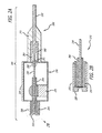
- FIGS. 2A - 2B are diagrams 200, 210 of the disclosed active alignment process to hermetically seal a photonic crystal based sensor 220, in accordance with at least one embodiment of the present disclosure. Similar to FIGS. 1A - 1C , the packaging of these figures may contain metal components or non-metal components. Also similar to FIGS. 1A - 1C , some items identified with reference numerals in these figures may dually represent items that are manufactured from metal components and items that are manufactured from non-metal components.
- FIGS. 2A - 2B depict the disclosed hermetically sealed photonic crystal sensor 220 using an active fiber alignment technique to attach to a multimode fiber 230 for aerospace applications.
- This approach provides a process for photonic crystal sensor packaging where high precision active alignment of the optical fiber 230 to the photonic crystal sensor 220 is critical.
- this approach starts with a main package body 240 that has two integrated snouts 250, 260, which are also referred to as nose tubes 250, 260.
- the snout 250 located at the front side of the package body 240 (i.e.
- front snout 250 is for the attachment of the silicon-on-insulator (SOI) photonic crystal sensor 220 to the package body 240; and snout 260 located at the back side (i.e. back snout 260) of the package body 140 is for the attachment of the optical fiber 230 to the package body 240.
- SOI silicon-on-insulator
- a fiber pedestal 270 that is used to attach the optical fiber 230 to the inside the package body 240 after active alignment of the fiber 230 to the photonic crystal sensor 220 is performed.
- This particular attachment process is referred to as the "fiber locking" process, which is a crucial step to lock the fiber 230 at its optimum optically aligned position to the photonic crystal sensor 220.
- a lid 280 At the top of the package body 240 is a lid 280, which is used as the final seal of the package body 240 after the fiber 230 alignment, attachment to the package pedestal 270, and fiber seal to the package wall at the back snout are complete.
- the main package body 240 and the lid 280 are made of kovar plated with gold.
- the package body 240 and the lid 280 are manufactured from ceramics, such as alumina or aluminum nitride (AIN).
- AIN aluminum nitride
- the SOI sensor 220 is attached to the front snout 250 of the package body 240.
- the SOI sensor 220 is attached to the front snout 250 by using high temperature solders, such as a lead tin (PbSn) solder or a gold tin (AuSn) solder.
- the SOI sensor 220 is attached to the front snout 250 by using a high temperature solder glass or epoxy. This attachment process will coarsely align the sensor 220 to the center of the front snout 250 to facilitate subsequent steps for fine active fiber alignment.
- a pre-metalized pattern is formed on the sensor 220 to match the size and shape of the front snout's 250 circumference.
- High temperature soldering of the snout 250 circumference to the sensor 220 is achieved by a self-alignment soldering process.
- the self alignment process utilizes the surface tension of the reflow solder to automatically align the center of the sensor 220 to the center axis of the front snout upon solidification of the solder.
- a circular-shaped high-temperature solder-glass preform which matches the diameter of the front snout 250, is used to seal the sensor 220 to the front snout 250.
- An additional layer of military grade epoxy 255 is added to the outer surface of the front snout to protect the side wall of the sensor 220; it also strengthens the attachment of the sensor 220 to the front snout.
- the optical fiber 230 is inserted into the package body 240 through the back snout 260 of the package body 240.
- the fiber 230 is partially metalized for solder joining of the fiber 230 to the pedestal 270 inside of the package body 240.
- metallization of the fiber is not needed.
- the optical fiber 230 has the option to attach to a ceramic ferrule 290 to strengthen the fiber 230 tip section for a highly vibratory environment. Attachment of the ferrule 290 to the fiber 230 is achieved by a high temperature epoxy or solder glass without using a metal solder.
- Active alignment of the fiber 230 to the sensor 220 is accomplished by holding the fiber 230 with a pair of fiber tweezers (not shown) that are attached to a high precision three-dimensional micro-positioner (not shown).
- the fiber 230 is moved to its optimum position by inputting a light signal to the fiber 230 which illuminates the sensor 220 surface, and the reflection spectrum from the sensor 220 is monitored during the fiber alignment process.
- the fiber 220 (with or without the ferrule 290) is "locked" on fiber pedestal 270 by either a high temperature solder, solder glass, or epoxy, depending upon the sensor's 220 target application.
- a high temperature solder glass or epoxy is used instead of a metallic high temperature solder.
- the fiber 230 is sealed at the back snout 260 of the package body 240.
- a short section of the fiber 230 at the package 240 wall location by the back snout is pre-coated with a gold/nickel (Au/Ni) layer 245 for hermetic sealing of the fiber 230 to the package 240 wall.
- Au/Ni gold/nickel
- This metalized fiber 230 to metal package 240 wall sealing process is accomplished with solder preforms heated by a localized RF induction furnace or a high temperature hot-tweezers heater applied to the back snout.
- the fiber 230 to package 240 seal is performed by melting non-conductive solder glass preforms or by a plotting a high temperature epoxy at the fiber and package wall interface 265.
- a fiber boot 295 is attached to the back snout 260 over the fiber 230 pigtail by a fully cured space-grade epoxy; additional steps are taken to ensure that no air bubbles are embedded inside the cured epoxy.
- the function of the fiber boot 295 is to limit the bending of the fiber 230 pigtail so as to not exceed its allowable bend radius; this will prevent fiber 230 breakage at the back snout 260 of the package body 240.
- the entire package 205 i.e. the package body 240 including the sensor 220, the fiber 230, the fiber pedestal 270, the optional ferrule 290, the fiber jacket 292, and the fiber boot 295) is placed inside a nitrogen purged seam sealer (also called a dry box).
- the entire package 205 is first heated for a several hours for out-gassing. After the entire package 205 is fully out-gassed, the sealing of a lid 280 on the top of the package body 240 will be performed.
- a metal (e.g., kovar) lid 280 is high temperature sealed to the top edges of the package body 240 by a pair of automatic rolling heaters.
- the package body 240 is first placed on a stage that can rotate ninety (90) degrees during the lid sealing process.
- the metal lid 280 is placed on top of the package body 240.
- a pair of rolling heaters (not shown) first makes contact to the first two parallel edges of the package lid 280.
- the rollers are then heated, and rolled along the first two parallel lid edges to seal the lid 280 to the package body 240.
- the package body 240 is rotated 90 degrees, and the rollers repeat the heating process to seal the other two parallel edges of lid 280 to the package body 240.
- This lid-to-package sealing process with a pair of rolling heaters is also called a "parallel seam welding process".
- the lid 280 will be made from a ceramic material, and a solder glass preform matching the perimeter of the package body's 240 top edge is put on the package body's 240 top edge. Then the ceramic lid 280 is placed on top of the solder glass preform.
- the pair of rolling heaters performs a similar parallel seam welding process like the process described for the metal packaging, except the temperature of the heater rollers is set at the solder glass's melting temperature.
- the whole package 205 is tested for hermeticity with a Helium leak tester.
- a leak rate less than approximately 1 E-6 cc/min is commonly considered to be an acceptable hermetic photonic crystal sensor package.
- FIG. 3 is a flow diagram 300 for the disclosed passive alignment process to hermetically seal a photonic crystal based sensor with metal components, in accordance with at least one embodiment of the present disclosure.
- a sensor chip is metalized with a donut pattern 320.
- the donut pattern matches the diameter and the wall thickness of a kovar tube.
- the sensor chip is centered to the center axis of an end of the kovar tube 330.
- the sensor chip is soldered to the end of the kovar tube to form a sensor chip assembly 340.
- a fiber is metalized 350. Then, a metal ferrule is assembled with the metalized fiber by soldering the metalized fiber inside of the metal ferrule 360. After the metalized fiber is soldered, the metal ferrule is inserted inside the kovar tube of the sensor chip assembly 370. Then, an end of the metalized fiber is aligned to the sensor chip of the sensor chip assembly 380. After the metalized fiber is aligned, at least a portion of the outer surface of the metal ferrule is soldered to at least a portion of the inner surface of the kovar tube of the sensor chip assembly 390. After the outer surface of the metal ferrule is soldered to at least a portion of the inner surface of the kovar tube, the process ends 395.
- FIG. 4 is a flow diagram 400 for the disclosed passive alignment process to hermetically seal a photonic crystal based sensor with non-metal components, in accordance with at least one embodiment of the present disclosure.
- a sensor chip is coated with a glass solder donut pattern 420.
- the glass solder donut pattern matches the diameter and the wall thickness of ceramic tube.
- the sensor chip is then centered to the center axis of an end of the ceramic tube 430. After the sensor chip is centered, the sensor chip is soldered to the end of the ceramic tube to form a sensor chip assembly 440.
- a ceramic ferrule is assembled with a fiber by soldering the fiber inside of the ceramic ferrule 450. After the fiber is soldered, the ceramic ferrule is inserted inside the ceramic tube of the sensor chip assembly 460. An end of the fiber is then aligned to the sensor chip of the sensor chip assembly 470. After the fiber is aligned, at least a portion of the outer surface of the ceramic ferrule is soldered to at least a portion of the inner surface of the ceramic tube of the sensor chip assembly 480. After the outer surface of the ceramic ferrule is soldered to at least a portion of the inner surface of the ceramic tube, the process ends 490.
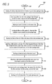
- FIG. 5 is a flow diagram 500 for the disclosed active alignment process to hermetically seal a photonic crystal based sensor with either metal or non-metal components, in accordance with at least one embodiment of the present disclosure.
- a sensor chip is sealed to an end of a front snout of a main package body 510.
- a fiber is inserted into the main package body through an end of a back snout 515.
- the end of the fiber is then aligned to the sensor chip 520.
- the fiber is locked to a fiber pedestal, where the fiber pedestal is located inside the main package body 525.
- the fiber is sealed at the end of the back snout of the main package body 530.
- a fiber jacket is then applied to an end of the fiber that is opposite the end of the fiber that is aligned to the sensor chip, where a portion of the fiber jacket is located inside of the back snout of the main package body 535. Then, the internal cavity of the back snout is sealed 540. A fiber boot is then attached to the end of the back snout and to at least a portion of the fiber jacket 545. Then, out-gassing of the main package body, the sensor chip, the fiber, the fiber pedestal, the fiber jacket, and the fiber boot is performed 550. After the out-gassing is performed, a lid is sealed to the top side of the main package body 555. After the lid is sealed to the main package body, the process ends 560.
Landscapes
- Physics & Mathematics (AREA)
- General Physics & Mathematics (AREA)
- Optics & Photonics (AREA)
- Crystallography & Structural Chemistry (AREA)
- Microelectronics & Electronic Packaging (AREA)
- Chemical & Material Sciences (AREA)
- Engineering & Computer Science (AREA)
- Electromagnetism (AREA)
- Optical Couplings Of Light Guides (AREA)
- Mechanical Coupling Of Light Guides (AREA)
- Optical Transform (AREA)
- Investigating Or Analysing Materials By Optical Means (AREA)
- Measurement Of Mechanical Vibrations Or Ultrasonic Waves (AREA)
- Photometry And Measurement Of Optical Pulse Characteristics (AREA)
Abstract
Description
- The present disclosure relates to photonic crystals. In particular, it relates to ruggedized photonic crystal sensor packagings.
- The present disclosure relates to a method, system, and apparatus for a ruggedized photonic crystal sensor packaging. In one or more embodiments, a disclosed method for hermetically sealing a sensor chip involves metalizing the sensor chip with a donut pattern. In one or more embodiments, the donut pattern matches the diameter and the wall thickness of a kovar tube. The method further involves centering the sensor chip to the center axis of an end of the kovar tube. Also, the method involves soldering the sensor chip to the end of the kovar tube to form a sensor chip assembly. In addition, the method involves metalizing a fiber (i.e. an optical fiber). In addition, the method involves assembling a metal ferrule with the metalized fiber by soldering the metalized fiber inside the metal ferrule. Additionally, the method involves inserting the metal ferrule inside the kovar tube of the sensor chip assembly. In addition, the method involves aligning an end of the metalized fiber to the sensor chip of the sensor chip assembly. Further, the method involves soldering the outer surface of the metal ferrule to the inner surface of the kovar tube of the sensor chip assembly.
- In one or more embodiments, a three-axis stage tool is used to center the sensor chip to the center axis of the kovar tube. In at least one embodiment, a three-axis stage tool is used to align the end of the metalized fiber to the sensor chip. In some embodiments, radio frequency (RF) induction heating is used for the soldering of the sensor chip to the end of the kovar tube. In one or more embodiments, RF induction heating and a donut shaped solder preform are used for the soldering of the outer surface of the metal ferrule to the inner surface of the kovar tube.
- In at least one embodiment, a method for hermetically sealing a sensor chip involves coating the sensor chip with a glass solder donut pattern. In one or more embodiments, the glass solder donut pattern matches the diameter and the wall thickness of a ceramic tube. The method further involves centering the sensor chip to a center axis of an end of the ceramic tube. Also, the method involves soldering the sensor chip to the end of the ceramic tube to form a sensor chip assembly. Additionally, the method involves assembling a ceramic ferrule with a fiber by soldering the fiber inside the ceramic ferrule. Also, the method involves inserting the ceramic ferrule inside the ceramic tube of the sensor chip assembly. In addition, the method involves aligning an end of the fiber to the sensor chip of the sensor chip assembly. Further, the method involves soldering the outer surface of the ceramic ferrule to the inner surface of the ceramic tube of the sensor chip assembly.
- In one or more embodiments, a three-axis stage tool is used to center the sensor chip to the center axis of the ceramic tube. In some embodiments, a three-axis stage tool is used to align the end of the fiber to the sensor chip. In at least one embodiment, localized thermal heating with solder glass is used for the soldering of the sensor chip to the end of the ceramic tube. In one or more embodiments, localized thermal heating and a donut-shaped glass solder preform are used for the soldering of the outer surface of the ceramic ferrule to the inner surface of the ceramic tube.
- In at least one embodiment, a method for hermetically sealing a sensor chip involves sealing the sensor chip to an end of a front snout of a main package body. The method further involves inserting a fiber into an end of a back snout of the main package body. Also, the method involves aligning an end of the fiber to the sensor chip. In addition, the method involves locking the fiber on a fiber pedestal. In one or more embodiments, the fiber pedestal is located inside the main package body. In addition, the method involves sealing the fiber at the end of the back snout of the main package body. Additionally, the method involves applying a fiber jacket to an end of the fiber that is opposite the end of the fiber that is aligned to the sensor chip, where a portion of the fiber jacket is located inside of the back snout of the main package body. In addition, the method involves sealing the internal cavity of the back snout. Also, the method involves attaching a fiber boot to the end of the back snout and to at least a portion of the fiber jacket. In addition, the method involves out-gassing the main package body, the sensor chip, the fiber, the fiber pedestal, the fiber jacket, and the fiber boot. Further, the method involves sealing a lid to the top side of the main package body.
- In one or more embodiments, the sealing of the sensor chip to the front snout is achieved by a self-alignment process that utilizes the surface tension of reflowed solder to center the sensor chip to a center axis of the front snout automatically when the solder is cooled and solidified. In at least one embodiment, a high precision three-dimensional micro-positioner is used for the aligning of the end of the fiber to the sensor chip. In some embodiments, the disclosed method further involves applying a protective layer of military grade epoxy to the outer surface of the front snout to protect the side wall of the sensor chip and to strengthen the sealing of the sensor chip to the front snout.
- In one or more embodiments, the disclosed method further involves at least partially metalizing the fiber. For this method, in some embodiments, the sealing of the sensor chip to the end of the front snout is achieved by using high temperature solders, and by metalizing the sensor chip with a pattern that matches the size and the shape of the circumference of the end of the front snout. In at least one embodiment, the high temperature solders are a lead tin (PbSn) solder and/or a gold tin (AuSn) solder. Also for this method, in one or more embodiments, a high temperature solder is used for the locking of the fiber on the fiber pedestal. In addition, in some embodiments, for this method, solder performs are used for the sealing of the fiber at the end of the back snout. For this method, the lid is a metal lid. Also for this method, in at least one embodiment, rolling heaters are used for the sealing of the metal lid to the top side of the main package body.
- In at least one embodiment, the sealing of the sensor chip to the end of the front snout is achieved by using a circular-shape high-temperature solder-glass perform that matches the diameter of the end of the front snout or a high temperature epoxy. In at least one embodiment, the method further comprises attaching a ceramic ferrule to at least a portion of the fiber. In some embodiments, the attaching of the ceramic ferrule to at least a portion of the fiber is achieved by using a high temperature epoxy or a high temperature solder glass. In one or more embodiments, the locking of the fiber on the fiber pedestal is achieved by using a high temperature solder glass or a high temperature epoxy. In at least one embodiment, the sealing of the fiber at the end of the back snout is achieved by melting a non-conductive solder glass perform or by plotting a high temperature epoxy at the location where the fiber and the wall of the main package body interface. In some embodiments, the lid is a ceramic lid. In at least one embodiment, the sealing of the ceramic lid to the top side of the main package body is achieved by using a solder glass perform that matches the perimeter of the edges of the top side of the main package body and by using rolling heaters for the sealing.
- In the figures and the text, in one aspect, a method is disclosed for hermetically sealing a
sensor chip 130, the method includes metalizing thesensor chip 130 with a donut pattern, wherein the donut pattern matches a diameter and a wall thickness of akovar tube 140; centering thesensor chip 130 to a center axis of an end of thekovar tube 140; soldering thesensor chip 130 to the end of thekovar tube 140 to form asensor chip assembly 170; metalizing afiber 160; assembling ametal ferrule 150 with themetalized fiber 160 by soldering themetalized fiber 160 inside themetal ferrule 150; inserting themetal ferrule 150 inside thekovar tube 140 of thesensor chip assembly 170; aligning an end of themetalized fiber 160 to thesensor chip 130 of thesensor chip assembly 170; and soldering an outer surface of the metal ferrule !50 to an inner surface of the kovar tube !40 of the sensor chip assembly. - In one variant, the method includes wherein a three-axis stage tool is used to center the
sensor chip 130 to the center axis of thekovar tube 140. In another variant, the method includes wherein a three-axis stage tool is used to align the end of themetalized fiber 160 to thesensor chip 130. In yet another variant, the method includes wherein radio frequency RF induction heating is used for the soldering of thesensor chip 130 to the end of thekovar tube 140. - In still yet another variant, the method includes wherein RF induction heating and a donut shaped
solder preform 180 are used for the soldering of the outer surface of themetal ferrule 150 to the inner surface of thekovar tube 140. - In one aspect, a method is disclosed for hermetically sealing a
sensor chip 130, the method including coating thesensor chip 130 with a glass solder donut pattern, wherein the glass solder donut pattern matches a diameter and a wall thickness of aceramic tube 140; centering thesensor chip 130 to a center axis of an end of theceramic tube 140; soldering thesensor chip 130 to the end of theceramic tube 140 to form asensor chip assembly 170; assembling aceramic ferrule 150 with afiber 160 by soldering thefiber 160 inside theceramic ferrule 150; inserting theceramic ferrule 150 inside theceramic tube 140 of thesensor chip assembly 170; aligning an end of thefiber 160 to thesensor chip 130 of thesensor chip assembly 170; and soldering an outer surface of theceramic ferrule 150 to an inner surface of theceramic tube 140 of thesensor chip assembly 170. - In one variant, the method includes wherein a three-axis stage tool is used to center the
sensor chip 130 to the center axis of theceramic tube 140. In another variant, the method includes wherein a three-axis stage tool is used to align the end of thefiber 160 to thesensor chip 130. In yet another variant, the method includes wherein localized thermal heating with solder glass is used for the soldering of thesensor chip 130 to the end of theceramic tube 140. In yet another variant, the method includes wherein localized thermal heating and a donut-shapedglass solder preform 180 are used for the soldering of the outer surface of theceramic ferrule 150 to the inner surface of theceramic tube 140. - In one aspect, a method is disclosed for hermetically sealing a sensor chip 220, the method including: sealing the sensor chip 220 to an end of a front snout 250 of a main package body 140; inserting a fiber 230 into the main package body 240 through an opening of a back snout 260 of the main package body 240; aligning an end of the fiber 230 to the sensor chip 220; locking the fiber 230 on a fiber pedestal 270, wherein the fiber pedestal 270 is located inside the main package body 240; sealing the fiber 230 at the end of the back snout 260 of the main package body 240; applying a fiber jacket 292 to an end of the fiber 230 opposite the end of the fiber 230 that is aligned to the sensor chip 220, wherein a portion of the fiber jacket 292 is located inside of the back snout 260 of the main package body 240; sealing an internal cavity of the back snout 260; attaching a fiber boot 295 to the end of the back snout 260 and to at least a portion of the fiber jacket 292; out-gassing the main package body 240, the sensor chip 220, the fiber 230, the fiber pedestal 270 , the fiber jacket 292, and the fiber boot 295; and sealing a lid to a top side of the main package body 240.
- In one variant, the method includes wherein the sealing of the
sensor chip 220 to thefront snout 250 is achieved by a self-alignment process that utilizes surface tension of reflowed solder to center thesensor chip 220 to a center axis of thefront snout 250 of automatically when the solder is cooled and solidified. In another variant, the method includes wherein the method further comprises at least partially metalizing thefiber 230. In yet another variant, the method includes wherein the sealing of thesensor chip 220 to the end of thefront snout 250 is achieved by using high temperature solders, and by metalizing thesensor chip 220 with a pattern that matches a size and a shape of a circumference of the end of thefront snout 250. In still yet another variant, the method includes wherein the high temperature solders are at least one of a lead tin PbSn solder and a gold tin AuSn solder. - In one example, the method includes wherein the method further comprises applying a protective layer of military grade epoxy to an outer surface of the
front snout 250 to protect a side wall of thesensor chip 220 and to strengthen the sealing of thesensor chip 220 to thefront snout 250. In another example, the method includes wherein a high temperature solder is used for the locking of thefiber 230 on thefiber pedestal 270. In yet another example, the method includes wherein solder performs are used for the sealing of the fiber at the end of theback snout 260. In still another example, the method includes wherein thelid 280 is ametal lid 280. - In one instance, the method includes wherein rolling heaters are used for the sealing of the
metal lid 280 to the top side of themain package body 240. In another instance, the method includes wherein a high precision three-dimensional micro-positioner is used for the aligning of the end of thefiber 230 to thesensor chip 220. In yet another instance, the method includes wherein the sealing of thesensor chip 220 to the end of thefront snout 250 is achieved by using a circular-shape high-temperature solder-glass perform that matches a diameter of the end of thefront snout 250, and by using one of a high temperature solder glass and a high temperature epoxy. In still yet another instance, the method of claim 11, wherein the method further comprises attaching aceramic ferrule 290 to at least a portion of thefiber 230. In yet another instance, the method includes wherein the attaching of theceramic ferrule 290 to the at least a portion of thefiber 230 is achieved by using at least one of a high temperature epoxy and a high temperature solder glass. - In one alternative, the method includes wherein the locking of the
fiber 230 on thefiber pedestal 270 is achieved by using at least one of a high temperature solder glass and a high temperature epoxy. In another alternative, the method includes wherein the sealing of thefiber 230 at the end of theback snout 260 is achieved by one of melting a non-conductive solder glass perform and plotting a high temperature epoxy at a location where thefiber 230 and wall of themain package body 240 interface. In yet another alternative, method includes wherein thelid 280 is aceramic lid 280. In still another alternative, the method includes wherein the sealing of theceramic lid 280 to the top side of themain package body 240 is achieved by using a solder glass perform that matches a perimeter of edges of the top side of themain package body 240 and by using rolling heaters for the sealing. - The features, functions, and advantages can be achieved independently in various embodiments of the present inventions or may be combined in yet other embodiments.
- These and other features, aspects, and advantages of the present disclosure will become better understood with regard to the following description, appended claims, and accompanying drawings where:
-
FIGS. 1A - 1C are diagrams of the disclosed passive alignment process to hermetically seal a photonic crystal based sensor, in accordance with at least one embodiment of the present disclosure. -
FIGS. 2A - 2B are diagrams of the disclosed active alignment process to hermetically seal a photonic crystal based sensor, in accordance with at least one embodiment of the present disclosure. -
FIG. 3 is a flow diagram for the disclosed passive alignment process to hermetically seal a photonic crystal based sensor with metal components, in accordance with at least one embodiment of the present disclosure. -
FIG. 4 is a flow diagram for the disclosed passive alignment process to hermetically seal a photonic crystal based sensor with non-metal components, in accordance with at least one embodiment of the present disclosure. -
FIG. 5 is a flow diagram for the disclosed active alignment process to hermetically seal a photonic crystal based sensor with either metal or non-metal components, in accordance with at least one embodiment of the present disclosure. - The methods and apparatus disclosed herein provide an operative system for a ruggedized photonic crystal sensor packaging. In particular, the present disclosure teaches ruggedized packaging photonic crystal (PC) sensor packaging that includes a hermetic-seal high-temperature jacket and a ferrule that eliminate the exposure of the optical fiber as well as the critical part of the photonic crystal sensor to harsh environments. The packaging methods described in the present disclosure enable photonic crystal based sensors to operate in demanding aerospace environments.
- Currently, fiber interferometer and fiber Bragg grating sensors are optical sensors that are attractive for many applications (such as for obtaining physical, chemical, and biological measurements) because of their structural simplicity, excellent reliability, high sensitivity, and capability of operating under critical and extreme conditions. However, the costs and sizes of these sensor systems limit their application. Such devices tend to only be suitable for laboratory use because they are heavy, bulky, and expensive.
- The packaging approaches described in the present disclosure enable remote sensing in challenging environments where adverse environmental conditions, such as electromagnetic interference (EMI), corrosive fluids, large temperature variations, and strong mechanical vibrations, currently exclude the use of traditional sensor technologies. For example, employing optical fuel sensors and interconnects on modern aircraft will substantially reduce the weight and improve performance to provide a significant cost savings. Further cost savings derive from the sensors' robustness to EMI, temperature variations, corrosive media, and vibrations, which simplify the packaging and integration of these sensors into modern aircraft.
- In the following description, numerous details are set forth in order to provide a more thorough description of the system. It will be apparent, however, to one skilled in the art, that the disclosed system may be practiced without these specific details. In the other instances, well known features have not been described in detail so as not to unnecessarily obscure the system.
- The present disclosure teaches two approaches to implement the disclosed ruggedized hermetic photonic crystal sensor packaging. These two approaches are: (1) packaging the photonic crystal sensor with a passive fiber alignment process to hermetically seal the sensor, and (2) packaging the photonic crystal sensor with an active fiber alignment process to hermetically seal the sensor. The description of the following figures will describe these two different approaches.
-
FIGS. 1A - 1C are diagrams 100, 110, 120 of the disclosed passive alignment process to hermetically seal a photonic crystal basedsensor 130, in accordance with at least one embodiment of the present disclosure. For the ruggedized photonic crystal sensor packaging shown in these three figures, it should be noted that the packaging may contain metal components or non-metal components. It should also be noted that for these three figures, some items identified with reference numerals may dually represent items that are manufactured from metal components and items that are manufactured from non-metal components (e.g., when the packaging contains metal components,item 140 represents a kovar tube; and when the packaging contains non-metal components,item 140 represents a ceramic tube). - When the packaging contains metal components, at the start of the process a photonic crystal based
sensor chip 130 is metalized with a donut pattern (not shown) that matches the diameter and the wall thickness of akovar tube 140 to allow soldering of thesensor chip 130 to the end of thekovar tube 140, thereby forming asensor chip assembly 170. Radio frequency (RF) induction heating is used for this localized soldering. A three-axis stage and a microscope are used to center thesensor chip 130 to the center axis of thekovar tube 140. - Then, a
metal ferrule 150 with a metalizedfiber 160 is assembled by soldering thefiber 160 inside of theferrule 150. Theferrule 150 is then inserted inside thekovar tube 140 of thesensor chip assembly 170. Thekovar tube 140 with attachedsensor chip 130 is aligned to the ferruleoptical fiber 160 using a three-axis stage to align the end of thefiber 160 to thesensor chip 130. After thesensor chip 130 is correctly aligned to thefiber 160, a portion of outer diameter of theferrule 150 is soldered to a portion of the inner diameter of thekovar tube 140 using RF induction heating and a donut shaped solder perform 180. - When the packaging contains non-metal components, at the start of the process a photonic crystal based
sensor chip 130 is coated with a glass solder donut pattern (not shown) that matches the diameter and the wall thickness of theceramic tube 140 to allow soldering of thesensor chip 130 to the end of theceramic tube 140, thereby forming asensor chip assembly 170. Localized thermal heating can be used with solder glass for this soldering process. A three-axis stage and microscope are used to center thesensor chip 130 to the center axis of theceramic tube 140. - After the
sensor chip 130 is soldered to the end of theceramic tube 140, aceramic ferrule 150 with anoptical fiber 160 is assembled using solder glass to attach thefiber 160 inside of theferrule 150. Then, theferrule 150 is inserted inside theceramic tube 140 of thesensor chip assembly 170. Theceramic tube 140 with the attachedsensor chip 130 is aligned to the ferruleoptical fiber 160 using a three-axis stage to align the end of thefiber 160 to thesensor chip 130. When thesensor chip 130 is correctly aligned to thefiber 160, a portion of the outer diameter offerrule 150 is soldered to the inner diameter of theceramic tube 140 by using localized thermal heating and a donut-shaped glass solder perform 180. -
FIGS. 2A - 2B are diagrams 200, 210 of the disclosed active alignment process to hermetically seal a photonic crystal basedsensor 220, in accordance with at least one embodiment of the present disclosure. Similar toFIGS. 1A - 1C , the packaging of these figures may contain metal components or non-metal components. Also similar toFIGS. 1A - 1C , some items identified with reference numerals in these figures may dually represent items that are manufactured from metal components and items that are manufactured from non-metal components. - In particular,
FIGS. 2A - 2B depict the disclosed hermetically sealedphotonic crystal sensor 220 using an active fiber alignment technique to attach to amultimode fiber 230 for aerospace applications. This approach provides a process for photonic crystal sensor packaging where high precision active alignment of theoptical fiber 230 to thephotonic crystal sensor 220 is critical. As shown in these figures, this approach starts with amain package body 240 that has twointegrated snouts nose tubes snout 250 located at the front side of the package body 240 (i.e. front snout 250) is for the attachment of the silicon-on-insulator (SOI)photonic crystal sensor 220 to thepackage body 240; andsnout 260 located at the back side (i.e. back snout 260) of thepackage body 140 is for the attachment of theoptical fiber 230 to thepackage body 240. - Inside the
package body 240 is afiber pedestal 270 that is used to attach theoptical fiber 230 to the inside thepackage body 240 after active alignment of thefiber 230 to thephotonic crystal sensor 220 is performed. This particular attachment process is referred to as the "fiber locking" process, which is a crucial step to lock thefiber 230 at its optimum optically aligned position to thephotonic crystal sensor 220. At the top of thepackage body 240 is alid 280, which is used as the final seal of thepackage body 240 after thefiber 230 alignment, attachment to thepackage pedestal 270, and fiber seal to the package wall at the back snout are complete. For sensor applications where metal packaging is allowed, themain package body 240 and thelid 280 are made of kovar plated with gold. For sensor applications where the use of metal is not allowed (e.g., for fuel and/or explosive gas sensors), thepackage body 240 and thelid 280 are manufactured from ceramics, such as alumina or aluminum nitride (AIN). The details of the packaging processes ofFIGS. 2A - 2B are described below. - At the beginning of the process, the
SOI sensor 220 is attached to thefront snout 250 of thepackage body 240. For a metal packaging, theSOI sensor 220 is attached to thefront snout 250 by using high temperature solders, such as a lead tin (PbSn) solder or a gold tin (AuSn) solder. For a ceramic packaging, theSOI sensor 220 is attached to thefront snout 250 by using a high temperature solder glass or epoxy. This attachment process will coarsely align thesensor 220 to the center of thefront snout 250 to facilitate subsequent steps for fine active fiber alignment. A pre-metalized pattern is formed on thesensor 220 to match the size and shape of the front snout's 250 circumference. High temperature soldering of thesnout 250 circumference to thesensor 220 is achieved by a self-alignment soldering process. The self alignment process utilizes the surface tension of the reflow solder to automatically align the center of thesensor 220 to the center axis of the front snout upon solidification of the solder. For a non-metal packaging, a circular-shaped high-temperature solder-glass preform, which matches the diameter of thefront snout 250, is used to seal thesensor 220 to thefront snout 250. An additional layer ofmilitary grade epoxy 255 is added to the outer surface of the front snout to protect the side wall of thesensor 220; it also strengthens the attachment of thesensor 220 to the front snout. - Next, the
optical fiber 230 is inserted into thepackage body 240 through theback snout 260 of thepackage body 240. For a metal packaging, thefiber 230 is partially metalized for solder joining of thefiber 230 to thepedestal 270 inside of thepackage body 240. For a ceramic packaging, metallization of the fiber is not needed. Also for a ceramic packaging, theoptical fiber 230 has the option to attach to aceramic ferrule 290 to strengthen thefiber 230 tip section for a highly vibratory environment. Attachment of theferrule 290 to thefiber 230 is achieved by a high temperature epoxy or solder glass without using a metal solder. Active alignment of thefiber 230 to thesensor 220 is accomplished by holding thefiber 230 with a pair of fiber tweezers (not shown) that are attached to a high precision three-dimensional micro-positioner (not shown). Thefiber 230 is moved to its optimum position by inputting a light signal to thefiber 230 which illuminates thesensor 220 surface, and the reflection spectrum from thesensor 220 is monitored during the fiber alignment process. After thefiber 230 is actively aligned to thesensor 220 at its optimum position, the fiber 220 (with or without the ferrule 290) is "locked" onfiber pedestal 270 by either a high temperature solder, solder glass, or epoxy, depending upon the sensor's 220 target application. For a fuel sensor application, a high temperature solder glass or epoxy is used instead of a metallic high temperature solder. - After
fiber 230 is locked, thefiber 230 is sealed at theback snout 260 of thepackage body 240. For a metal packaging, a short section of thefiber 230 at thepackage 240 wall location by the back snout is pre-coated with a gold/nickel (Au/Ni)layer 245 for hermetic sealing of thefiber 230 to thepackage 240 wall. This metalizedfiber 230 tometal package 240 wall sealing process is accomplished with solder preforms heated by a localized RF induction furnace or a high temperature hot-tweezers heater applied to the back snout. For a non-metal (ceramic) packaging, thefiber 230 to package 240 seal is performed by melting non-conductive solder glass preforms or by a plotting a high temperature epoxy at the fiber andpackage wall interface 265. - After the
fiber 230 is sealed to thepackage 240 wall, additional epoxy is applied to fill theinner cavity 297 of theback snout 260, and the epoxy is cured with thefiber 230 pigtail's outer jacket (i.e. fiber jacket) 292 partially embedded inside thesnout 260 for strain relief. Afiber boot 295 is attached to theback snout 260 over thefiber 230 pigtail by a fully cured space-grade epoxy; additional steps are taken to ensure that no air bubbles are embedded inside the cured epoxy. The function of thefiber boot 295 is to limit the bending of thefiber 230 pigtail so as to not exceed its allowable bend radius; this will preventfiber 230 breakage at theback snout 260 of thepackage body 240. - After the
fiber 230 pigtail is attached, the entire package 205 (i.e. thepackage body 240 including thesensor 220, thefiber 230, thefiber pedestal 270, theoptional ferrule 290, thefiber jacket 292, and the fiber boot 295) is placed inside a nitrogen purged seam sealer (also called a dry box). Theentire package 205 is first heated for a several hours for out-gassing. After theentire package 205 is fully out-gassed, the sealing of alid 280 on the top of thepackage body 240 will be performed. For a metal packaging, a metal (e.g., kovar)lid 280 is high temperature sealed to the top edges of thepackage body 240 by a pair of automatic rolling heaters. Thepackage body 240 is first placed on a stage that can rotate ninety (90) degrees during the lid sealing process. Next, themetal lid 280 is placed on top of thepackage body 240. A pair of rolling heaters (not shown) first makes contact to the first two parallel edges of thepackage lid 280. The rollers are then heated, and rolled along the first two parallel lid edges to seal thelid 280 to thepackage body 240. Then, thepackage body 240 is rotated 90 degrees, and the rollers repeat the heating process to seal the other two parallel edges oflid 280 to thepackage body 240. This lid-to-package sealing process with a pair of rolling heaters is also called a "parallel seam welding process". For the case of a non-metal packaging, thelid 280 will be made from a ceramic material, and a solder glass preform matching the perimeter of the package body's 240 top edge is put on the package body's 240 top edge. Then theceramic lid 280 is placed on top of the solder glass preform. The pair of rolling heaters performs a similar parallel seam welding process like the process described for the metal packaging, except the temperature of the heater rollers is set at the solder glass's melting temperature. - After parallel seam sealing process is completed, the
whole package 205 is tested for hermeticity with a Helium leak tester. A leak rate less than approximately 1 E-6 cc/min is commonly considered to be an acceptable hermetic photonic crystal sensor package. -
FIG. 3 is a flow diagram 300 for the disclosed passive alignment process to hermetically seal a photonic crystal based sensor with metal components, in accordance with at least one embodiment of the present disclosure. At thestart 310 of the process, a sensor chip is metalized with adonut pattern 320. The donut pattern matches the diameter and the wall thickness of a kovar tube. Then, the sensor chip is centered to the center axis of an end of thekovar tube 330. After the sensor chip is centered, the sensor chip is soldered to the end of the kovar tube to form asensor chip assembly 340. - A fiber is metalized 350. Then, a metal ferrule is assembled with the metalized fiber by soldering the metalized fiber inside of the
metal ferrule 360. After the metalized fiber is soldered, the metal ferrule is inserted inside the kovar tube of thesensor chip assembly 370. Then, an end of the metalized fiber is aligned to the sensor chip of thesensor chip assembly 380. After the metalized fiber is aligned, at least a portion of the outer surface of the metal ferrule is soldered to at least a portion of the inner surface of the kovar tube of thesensor chip assembly 390. After the outer surface of the metal ferrule is soldered to at least a portion of the inner surface of the kovar tube, the process ends 395. -
FIG. 4 is a flow diagram 400 for the disclosed passive alignment process to hermetically seal a photonic crystal based sensor with non-metal components, in accordance with at least one embodiment of the present disclosure. At thestart 410 of the process, a sensor chip is coated with a glasssolder donut pattern 420. The glass solder donut pattern matches the diameter and the wall thickness of ceramic tube. The sensor chip is then centered to the center axis of an end of theceramic tube 430. After the sensor chip is centered, the sensor chip is soldered to the end of the ceramic tube to form asensor chip assembly 440. - Then, a ceramic ferrule is assembled with a fiber by soldering the fiber inside of the
ceramic ferrule 450. After the fiber is soldered, the ceramic ferrule is inserted inside the ceramic tube of thesensor chip assembly 460. An end of the fiber is then aligned to the sensor chip of thesensor chip assembly 470. After the fiber is aligned, at least a portion of the outer surface of the ceramic ferrule is soldered to at least a portion of the inner surface of the ceramic tube of thesensor chip assembly 480. After the outer surface of the ceramic ferrule is soldered to at least a portion of the inner surface of the ceramic tube, the process ends 490. -
FIG. 5 is a flow diagram 500 for the disclosed active alignment process to hermetically seal a photonic crystal based sensor with either metal or non-metal components, in accordance with at least one embodiment of the present disclosure. At thestart 505 of the process, a sensor chip is sealed to an end of a front snout of amain package body 510. Then, a fiber is inserted into the main package body through an end of aback snout 515. The end of the fiber is then aligned to thesensor chip 520. After the end of the fiber is aligned, the fiber is locked to a fiber pedestal, where the fiber pedestal is located inside themain package body 525. Then, the fiber is sealed at the end of the back snout of themain package body 530. - A fiber jacket is then applied to an end of the fiber that is opposite the end of the fiber that is aligned to the sensor chip, where a portion of the fiber jacket is located inside of the back snout of the
main package body 535. Then, the internal cavity of the back snout is sealed 540. A fiber boot is then attached to the end of the back snout and to at least a portion of thefiber jacket 545. Then, out-gassing of the main package body, the sensor chip, the fiber, the fiber pedestal, the fiber jacket, and the fiber boot is performed 550. After the out-gassing is performed, a lid is sealed to the top side of themain package body 555. After the lid is sealed to the main package body, the process ends 560. - Although certain illustrative embodiments and methods have been disclosed herein, it can be apparent from the foregoing disclosure to those skilled in the art that variations and modifications of such embodiments and methods can be made without departing from the true spirit and scope of the art disclosed. Many other examples of the art disclosed exist, each differing from others in matters of detail only. Accordingly, it is intended that the art disclosed shall be limited only to the extent required by the appended claims and the rules and principles of applicable law.
Claims (15)
- A method for hermetically sealing a sensor chip (220), the method comprising:sealing the sensor chip (220) to an end of a front snout (250) of a main package body (140);inserting a fiber (230) into the main package body (240) through an opening of a back snout (260) of the main package body (240);aligning an end of the fiber (230) to the sensor chip (220);locking the fiber (230) on a fiber pedestal (270), wherein the fiber pedestal (270) is located inside the main package body (240);sealing the fiber (230) at the end of the back snout (260) of the main package body (240);applying a fiber jacket (292) to an end of the fiber (230) opposite the end of the fiber (230) that is aligned to the sensor chip (220), wherein a portion of the fiber jacket (292) is located inside of the back snout (260) of the main package body (240);sealing an internal cavity of the back snout (260);attaching a fiber boot (295) to the end of the back snout (260) and to at least a portion of the fiber jacket (292);out-gassing the main package body (240), the sensor chip (220), the fiber (230), the fiber pedestal (270), the fiber jacket (292), and the fiber boot (295); andsealing a lid to a top side of the main package body (240).
- The method of claim 1, wherein the sealing of the sensor chip (220) to the front snout (250) is achieved by a self-alignment process that utilizes surface tension of reflowed solder to center the sensor chip (220) to a center axis of the front snout (250) of automatically when the solder is cooled and solidified.
- The method of any of claims 1 or 2, wherein the method further comprises at least partially metalizing the fiber (230).
- The method of any of claim 1-3, wherein the sealing of the sensor chip (220) to the end of the front snout (250) is achieved by using high temperature solders, and by metalizing the sensor chip (220) with a pattern that matches a size and a shape of a circumference of the end of the front snout (250).
- The method of claim 4, wherein the high temperature solders are at least one of a lead tin (PbSn) solder and a gold tin (AuSn) solder.
- The method of claim 1, wherein the method further comprises applying a protective layer of military grade epoxy to an outer surface of the front snout (250) to protect a side wall of the sensor chip (220) and to strengthen the sealing of the sensor chip (220) to the front snout (250); wherein a high temperature solder is used for the locking of the fiber (230) on the fiber pedestal (270); and wherein solder performs are used for the sealing of the fiber at the end of the back snout (260); and wherein rolling heaters are used for the sealing of a metal lid (280) to the top side of the main package body (240).
- The method of any of claims 1-6, wherein a high precision three dimensional micro-positioner is used for the aligning of the end of the fiber (230) to the sensor chip (220).
- The method of any of claims 1-7, wherein the sealing of the sensor chip (220) to the end of the front snout (250) is achieved by using a circular-shape high-temperature solder-glass perform that matches a diameter of the end of the front snout (250), and by using one of a high temperature solder glass and a high temperature epoxy.
- The method of any of claims 1-8, wherein the method further comprises attaching a ceramic ferrule (290) to at least a portion of the fiber (230); and wherein the attaching of the ceramic ferrule (290) to the at least a portion of the fiber (230) is achieved by using at least one of a high temperature epoxy and a high temperature solder glass.
- The method of claim 1, wherein the locking of the fiber (230) on the fiber pedestal (270) is achieved by using at least one of a high temperature solder glass and a high temperature epoxy; wherein the sealing of the fiber (230) at the end of the back snout (260) is achieved by one of melting a non-conductive solder glass perform and plotting a high temperature epoxy at a location where the fiber (230) and wall of the main package body (240) interface; and wherein the lid (280) is a ceramic lid (280).
- The method of claim 10, wherein the sealing of the ceramic lid (280) to the top side of the main package body (240) is achieved by using a solder glass perform that matches a perimeter of edges of the top side of the main package body (240) and by using rolling heaters for the sealing.
- A hermetically sealed a sensor chip (220) having a package comprising:a main package body (140) having an end of a front snout (250) sealed to the sensor chip (220);a fiber (230) inserted into the main package body (240) through an opening of a back snout (260) of the main package body (240);an end of the fiber (230) aligned to the sensor chip (220), the fiber (230) being locked on a fiber pedestal (270), the fiber pedestal (270) located inside the main package body (240) and the fiber (230) sealed at the end of the back snout (260) of the main package body (240);a fiber jacket (292) applied to an end of the fiber (230) opposite the end of the fiber (230) that is aligned to the sensor chip (220), wherein a portion of the fiber jacket (292) is located inside of the back snout (260) of the main package body (240);an internal cavity that is sealed of the back snout (260);a fiber boot (295) attached to the end of the back snout (260) and to at least a portion of the fiber jacket (292); wherein out-gassing of the main package body (240), the sensor chip (220), the fiber (230), the fiber pedestal (270), the fiber jacket (292), and the fiber boot (295) have been outgassed; anda lid that is sealed to a top side of the main package body (240).
- The package of claim 12, wherein an end of the front snout (250) sealed of the sensor chip (220) achieved by a self-alignment process that utilizes surface tension of reflowed solder to center the sensor chip (220) to a center axis of the front snout (250) of automatically when the solder is cooled and solidified; and wherein the package further comprises at least partially metalizing the fiber (230).
- The package of claim 12, wherein an end of the front snout (250) sealed to the sensor chip (220) is achieved by using high temperature solders, and by a metalized pattern on the sensor chip (220) that matches a size and a shape of a circumference of the end of the front snout (250); and wherein the high temperature solders are at least one of a lead tin (PbSn) solder and a gold tin (AuSn) solder.
- The package of any of claims 12-14, further comprising a protective layer of military grade epoxy applied to an outer surface of the front snout (250) to protect a side wall of the sensor chip (220) and to strengthen the front stout (250) seal to the sensor chip (220).
Applications Claiming Priority (1)
| Application Number | Priority Date | Filing Date | Title |
|---|---|---|---|
| US13/467,358 US9500808B2 (en) | 2012-05-09 | 2012-05-09 | Ruggedized photonic crystal sensor packaging |
Publications (3)
| Publication Number | Publication Date |
|---|---|
| EP2662676A2 true EP2662676A2 (en) | 2013-11-13 |
| EP2662676A3 EP2662676A3 (en) | 2014-01-01 |
| EP2662676B1 EP2662676B1 (en) | 2021-06-02 |
Family
ID=48128175
Family Applications (1)
| Application Number | Title | Priority Date | Filing Date |
|---|---|---|---|
| EP13164130.0A Active EP2662676B1 (en) | 2012-05-09 | 2013-04-17 | Ruggedised fibre coupled sensor package and method of packaging |
Country Status (5)
| Country | Link |
|---|---|
| US (3) | US9500808B2 (en) |
| EP (1) | EP2662676B1 (en) |
| JP (1) | JP6415021B2 (en) |
| CN (1) | CN103390595B (en) |
| RU (1) | RU2633675C2 (en) |
Cited By (2)
| Publication number | Priority date | Publication date | Assignee | Title |
|---|---|---|---|---|
| EP2765395A3 (en) * | 2013-02-12 | 2014-11-19 | The Boeing Company | Multifunctional optical sensor unit |
| US10654564B2 (en) | 2016-12-15 | 2020-05-19 | Safran Landing Systems Uk Ltd | Aircraft assembly including deflection sensor |
Families Citing this family (10)
| Publication number | Priority date | Publication date | Assignee | Title |
|---|---|---|---|---|
| US10209447B2 (en) * | 2015-09-11 | 2019-02-19 | Ii-Vi Incorporated | Micro splice protector |
| RU2629133C1 (en) * | 2016-09-27 | 2017-08-24 | Федеральное государственное бюджетное образовательное учреждение высшего образования "Саратовский национальный исследовательский государственный университет имени Н.Г. Чернышевского" | Method for selective soldering of external shells of photonic crystalline waveguides with hollow core |
| US10435170B2 (en) * | 2016-12-08 | 2019-10-08 | The Boeing Company | Systems and methods for installation of sensors for fuel quantity indicating systems |
| JP6935206B2 (en) * | 2017-02-14 | 2021-09-15 | 古河電気工業株式会社 | Optical element package and optical element module |
| CN110631658B (en) * | 2018-06-22 | 2024-12-13 | 谷轮环境科技(苏州)有限公司 | Test equipment and compressors for pressure equipment |
| RU192006U1 (en) * | 2019-05-24 | 2019-08-30 | Леонид Романович Боев | Microelectromechanical device |
| US12104933B2 (en) * | 2019-06-25 | 2024-10-01 | Nagano Keiki Co., Ltd. | Optical sensor and physical quantity measurement device |
| US12436345B2 (en) * | 2021-12-20 | 2025-10-07 | Intel Corporation | Immersion compatible optical interconnect |
| US12405432B2 (en) * | 2022-07-04 | 2025-09-02 | Sumitomo Electric Industries, Ltd. | Manufacturing method of optical module |
| CN118623920B (en) * | 2024-03-26 | 2025-10-31 | 西北工业大学 | High-temperature MEMS wall sensor, packaging method and application |
Family Cites Families (92)
| Publication number | Priority date | Publication date | Assignee | Title |
|---|---|---|---|---|
| US3093792A (en) * | 1960-03-16 | 1963-06-11 | Bendix Corp | Ion air density sensor for atmospheric pressure and altitude measurements |
| US3423594A (en) * | 1964-03-03 | 1969-01-21 | Anthony G Galopin | Photoelectric semiconductor device with optical fiber means coupling input signals to base |
| US3585454A (en) * | 1969-04-01 | 1971-06-15 | Westinghouse Electric Corp | Improved case member for a light activated semiconductor device |
| US4131905A (en) * | 1977-05-26 | 1978-12-26 | Electric Power Research Institute, Inc. | Light-triggered thyristor and package therefore |
| US4129042A (en) | 1977-11-18 | 1978-12-12 | Signetics Corporation | Semiconductor transducer packaged assembly |
| US4217179A (en) * | 1978-07-17 | 1980-08-12 | National Research Development Corporation | Determination of lithium, sensor therefor and method of making said sensor |
| FR2448727A1 (en) * | 1979-02-08 | 1980-09-05 | Thomson Csf | OPTO-ELECTRONIC COUPLING HEAD |
| US4399541A (en) * | 1981-02-17 | 1983-08-16 | Northern Telecom Limited | Light emitting device package having combined heater/cooler |
| US4615031A (en) * | 1982-07-27 | 1986-09-30 | International Standard Electric Corporation | Injection laser packages |
| JPS5994891A (en) * | 1982-11-24 | 1984-05-31 | Hitachi Ltd | Semiconductor laser device |
| DE3244882A1 (en) * | 1982-12-03 | 1984-06-07 | Siemens AG, 1000 Berlin und 8000 München | TRANSMITTER OR RECEIVER WITH A DIODE HOLDED BY MEANS OF A CARRIER |
| US4488773A (en) * | 1982-12-23 | 1984-12-18 | United Technologies Corporation | Optical fiber position sensor |
| DE3338315A1 (en) | 1983-10-21 | 1985-05-02 | Standard Elektrik Lorenz Ag, 7000 Stuttgart | OPTOELECTRIC COUPLING |
| JPS6123379A (en) | 1984-07-11 | 1986-01-31 | Hitachi Ltd | optoelectronic device |
| JPS61235731A (en) * | 1985-04-11 | 1986-10-21 | Sharp Corp | Pressure sensing element |
| JPH0632341B2 (en) | 1985-05-22 | 1994-04-27 | 株式会社日立製作所 | Semiconductor light emitting device with optical fiber |
| US4752109A (en) * | 1986-09-02 | 1988-06-21 | Amp Incorporated | Optoelectronics package for a semiconductor laser |
| US5068865A (en) * | 1988-06-09 | 1991-11-26 | Nec Corporation | Semiconductor laser module |
| US5011256A (en) * | 1988-10-28 | 1991-04-30 | E. I. Du Pont De Nemours And Company | Package for an opto-electronic component |
| SU1598700A1 (en) * | 1988-10-31 | 1996-10-10 | С.А. Алавердян | Method of manufacture of air-tight unit to match optical cable with body of device |
| US5123671A (en) * | 1989-03-13 | 1992-06-23 | Monroe Auto Equipment Company | Method and apparatus for controlling shock absorbers |
| JPH0317605A (en) * | 1989-06-15 | 1991-01-25 | Honda Motor Co Ltd | fiber optic transmission module |
| JPH0356831A (en) * | 1989-07-25 | 1991-03-12 | Fujitsu Ltd | Cooling type infrared detection device |
| US5112456A (en) * | 1989-12-12 | 1992-05-12 | Trustees Of The University Of Pennsylvania | Electrochemical sensors and methods for their use |
| US4979787A (en) * | 1990-01-12 | 1990-12-25 | Pco, Inc. | Optical-electronic interface module |
| JP2695995B2 (en) * | 1991-01-14 | 1998-01-14 | 株式会社東芝 | Optical semiconductor device |
| JPH0575011A (en) * | 1991-09-18 | 1993-03-26 | Nec Corp | Semiconductor device |
| JPH05167301A (en) * | 1991-12-16 | 1993-07-02 | Mitsubishi Materials Corp | Package structure |
| US5336389A (en) * | 1992-06-08 | 1994-08-09 | Her Majesty The Queen In Right Of Canada, As Represented By The Minister Of Energy, Mines And Resources | Long lasting alkali and alkaline earth metal sensor |
| IL107659A0 (en) * | 1993-11-18 | 1994-07-31 | State Of Israel Ministy Of Def | A hand-held infra red imaging probe |
| US5586207A (en) * | 1993-11-29 | 1996-12-17 | Northern Telecom Limited | Methods and assemblies for packaging opto-electronic devices and for coupling optical fibers to the packaged devices |
| US5613026A (en) | 1993-12-28 | 1997-03-18 | Sumitomo Osaka Cement Co., Ltd. | Package structure for optical element and fibers and composite structure thereof |
| US5434940A (en) * | 1994-03-24 | 1995-07-18 | The Whitaker Corporation | Active fiber needle |
| US5568585A (en) * | 1995-03-13 | 1996-10-22 | The United States Of America As Represented By The Department Of Energy | Low-temperature hermetic sealing of optical fiber components |
| US5571394A (en) * | 1995-05-08 | 1996-11-05 | General Electric Company | Monolithic sensor switch for detecting presence of stoichiometric H2 /O2 ratio in boiling water reactor circuit |
| US5685636A (en) * | 1995-08-23 | 1997-11-11 | Science And Engineering Associates, Inc. | Eye safe laser security device |
| US5870511A (en) * | 1997-01-27 | 1999-02-09 | Sentec Corporation | Fiber optic temperature sensor |
| JPH1010372A (en) * | 1996-06-20 | 1998-01-16 | Alps Electric Co Ltd | Ld module |
| US6351996B1 (en) | 1998-11-12 | 2002-03-05 | Maxim Integrated Products, Inc. | Hermetic packaging for semiconductor pressure sensors |
| CA2335529A1 (en) * | 1999-04-20 | 2000-10-26 | Yuichiro Irie | Laser diode module |
| US6213651B1 (en) * | 1999-05-26 | 2001-04-10 | E20 Communications, Inc. | Method and apparatus for vertical board construction of fiber optic transmitters, receivers and transceivers |
| US6181760B1 (en) * | 1999-07-20 | 2001-01-30 | General Electric Company | Electrochemical corrosion potential sensor with increased lifetime |
| US6398931B1 (en) * | 2000-01-31 | 2002-06-04 | Phoenix Electrode Company | Combination ion-selective electrode with a replaceable sensing membrane |
| US6330829B1 (en) * | 2000-03-16 | 2001-12-18 | Kulite Semiconductor Products Inc. | Oil-filled pressure transducer |
| ATE415644T1 (en) * | 2000-05-04 | 2008-12-15 | Schott Donnelly Llc | METHOD FOR PRODUCING AN ELECTROCHROMIC PANEL |
| US6827250B2 (en) * | 2001-06-28 | 2004-12-07 | Microchips, Inc. | Methods for hermetically sealing microchip reservoir devices |
| US6834154B2 (en) * | 2001-07-24 | 2004-12-21 | 3M Innovative Properties Co. | Tooling fixture for packaged optical micro-mechanical devices |
| US6771859B2 (en) * | 2001-07-24 | 2004-08-03 | 3M Innovative Properties Company | Self-aligning optical micro-mechanical device package |
| JP2003197797A (en) * | 2001-12-25 | 2003-07-11 | Herutsu Kk | Hermetic sealing method for piezoelectric element |
| JP2003329888A (en) * | 2002-05-14 | 2003-11-19 | Fdk Corp | Optical fiber mounting structure and optical device |
| US8169684B2 (en) * | 2002-09-30 | 2012-05-01 | Gentex Corporation | Vehicular rearview mirror elements and assemblies incorporating these elements |
| US7376312B2 (en) * | 2002-11-05 | 2008-05-20 | Rohm Co., Ltd. | Optical module and method for manufacturing the same |
| JP2004179258A (en) * | 2002-11-25 | 2004-06-24 | Hamamatsu Photonics Kk | UV sensor |
| US6922518B2 (en) * | 2002-12-13 | 2005-07-26 | Lighthouse Capital Partners | Methods and apparatus for sealed fiber optic feedthroughs |
| US6773171B2 (en) * | 2003-01-14 | 2004-08-10 | Intel Corporation | Optoelectronic housings and methods of assembling optoelectronic packages |
| US7149374B2 (en) * | 2003-05-28 | 2006-12-12 | The United States Of America As Represented By The Secretary Of The Navy | Fiber optic pressure sensor |
| JP4256212B2 (en) * | 2003-06-17 | 2009-04-22 | 浜松ホトニクス株式会社 | Photodetector tube |
| US7218657B2 (en) * | 2003-07-09 | 2007-05-15 | Sumitomo Electric Industries, Ltd. | Optical transmitting module having a can type package and providing a temperature sensor therein |
| EP1515364B1 (en) * | 2003-09-15 | 2016-04-13 | Nuvotronics, LLC | Device package and methods for the fabrication and testing thereof |
| US6900509B2 (en) * | 2003-09-19 | 2005-05-31 | Agilent Technologies, Inc. | Optical receiver package |
| JP2005165200A (en) | 2003-12-05 | 2005-06-23 | Seiko Instruments Inc | Optical device and manufacturing method thereof |
| US7173713B2 (en) * | 2004-03-04 | 2007-02-06 | Virginia Tech Intellectual Properties, Inc. | Optical fiber sensors for harsh environments |
| US20050195402A1 (en) * | 2004-03-04 | 2005-09-08 | Russell May | Crystalline optical fiber sensors for harsh environments |
| GB0408073D0 (en) * | 2004-04-08 | 2004-05-12 | Council Cent Lab Res Councils | Optical sensor |
| JP2005309153A (en) * | 2004-04-22 | 2005-11-04 | Murata Mfg Co Ltd | Package structure of optical module |
| EP1598686A3 (en) | 2004-05-17 | 2005-12-07 | JDS Uniphase Corporation | RF absorbing strain relief bushing |
| JP2006064680A (en) * | 2004-08-24 | 2006-03-09 | Photonic Science Technology Inc | Optical fiber vibration sensor |
| DE102004051468A1 (en) | 2004-10-22 | 2006-04-27 | Robert Bosch Gmbh | Method for mounting semiconductor chips and corresponding semiconductor chip arrangement |
| WO2007089246A2 (en) * | 2005-02-09 | 2007-08-09 | Giraffe Liquid Management Systems, Inc. | Adjustable height inlet/outlet liquid level management tools and systems |
| CA2599696C (en) * | 2005-03-02 | 2014-04-01 | Fiso Technologies Inc. | Fabry-perot optical sensor and method of manufacturing the same |
| CA2618685C (en) * | 2005-08-12 | 2015-02-03 | Fiso Technologies Inc. | Single piece fabry-perot optical sensor and method of manufacturing the same |
| US7561277B2 (en) * | 2006-05-19 | 2009-07-14 | New Jersey Institute Of Technology | MEMS fiber optic microphone |
| WO2008060389A2 (en) * | 2006-10-19 | 2008-05-22 | S3C, Incorporated | Sensor device package having thermally compliant die pad |
| US7559701B2 (en) * | 2007-03-19 | 2009-07-14 | General Electric Company | High-temperature pressure sensor and method of assembly |
| WO2009025662A1 (en) * | 2007-08-17 | 2009-02-26 | Em4, Inc. | Reducing heating from non-coupled light in power transmitting optical fibers |
| RU2506961C2 (en) | 2007-08-22 | 2014-02-20 | Дзе Рисерч Фаундейшн Оф Стейт Юниверсити Оф Нью Йорк | System and method for supply and shared use of breathing gas |
| WO2009026566A1 (en) | 2007-08-23 | 2009-02-26 | Cynvenio Biosystems, Llc | Trapping magnetic sorting system for target species |
| US7499605B1 (en) * | 2007-09-14 | 2009-03-03 | General Electric Company | Fiber Bragg grating for high temperature sensing |
| US7574075B2 (en) * | 2007-09-14 | 2009-08-11 | General Electric Company | Fiber Bragg grating and fabrication method |
| US7877009B2 (en) * | 2007-12-20 | 2011-01-25 | 3M Innovative Properties Company | Method and system for electrochemical impedance spectroscopy |
| US7697798B2 (en) * | 2008-02-11 | 2010-04-13 | The United States Of America As Represented By The Secretary Of The Navy | Fiber optic pressure sensors and catheters |
| AT505077B1 (en) * | 2008-06-06 | 2010-01-15 | Avl List Gmbh | MEASURING DEVICE |
| US8643127B2 (en) * | 2008-08-21 | 2014-02-04 | S3C, Inc. | Sensor device packaging |
| JP5470784B2 (en) * | 2008-09-12 | 2014-04-16 | オムロン株式会社 | Light receiving device and sensor device |
| US20110027438A1 (en) * | 2009-07-29 | 2011-02-03 | Finkowski James W | Hffs packaging method and apparatus for refrigerated dough |
| US9482927B2 (en) | 2009-10-26 | 2016-11-01 | The Boeing Company | Optical sensor interrogation system |
| US8342756B2 (en) * | 2009-12-22 | 2013-01-01 | Jds Uniphase Corporation | Hermetic seal between a package and an optical fiber |
| US8215850B2 (en) * | 2009-12-29 | 2012-07-10 | Prasad Yalamanchili | Optical module with fiber feedthrough |
| US8369671B2 (en) * | 2010-02-26 | 2013-02-05 | General Electric Company | Hermetically sealed fiber sensing cable |
| DE102010019813A1 (en) * | 2010-05-06 | 2011-11-10 | Siemens Aktiengesellschaft | Fiber optic vibration sensor |
| US8494312B2 (en) | 2010-08-18 | 2013-07-23 | The Boeing Company | Magnetically actuated photonic crystal sensor |
| CN102436045A (en) * | 2011-12-29 | 2012-05-02 | 武汉电信器件有限公司 | Installation and fixation structure of light-guide fiber of photoelectronic device |
-
2012
- 2012-05-09 US US13/467,358 patent/US9500808B2/en active Active
-
2013
- 2013-04-17 EP EP13164130.0A patent/EP2662676B1/en active Active
- 2013-05-06 RU RU2013120383A patent/RU2633675C2/en active
- 2013-05-07 JP JP2013097472A patent/JP6415021B2/en active Active
- 2013-05-08 CN CN201310166846.8A patent/CN103390595B/en active Active
-
2016
- 2016-10-14 US US15/294,584 patent/US10061093B2/en active Active
-
2018
- 2018-04-19 US US15/957,784 patent/US10338328B2/en active Active
Non-Patent Citations (1)
| Title |
|---|
| None |
Cited By (3)
| Publication number | Priority date | Publication date | Assignee | Title |
|---|---|---|---|---|
| EP2765395A3 (en) * | 2013-02-12 | 2014-11-19 | The Boeing Company | Multifunctional optical sensor unit |
| US9103968B2 (en) | 2013-02-12 | 2015-08-11 | The Boeing Company | Multifunctional optical sensor unit |
| US10654564B2 (en) | 2016-12-15 | 2020-05-19 | Safran Landing Systems Uk Ltd | Aircraft assembly including deflection sensor |
Also Published As
| Publication number | Publication date |
|---|---|
| US10338328B2 (en) | 2019-07-02 |
| US20170031116A1 (en) | 2017-02-02 |
| JP2013235000A (en) | 2013-11-21 |
| EP2662676B1 (en) | 2021-06-02 |
| US10061093B2 (en) | 2018-08-28 |
| EP2662676A3 (en) | 2014-01-01 |
| US20130298392A1 (en) | 2013-11-14 |
| RU2633675C2 (en) | 2017-10-16 |
| CN103390595A (en) | 2013-11-13 |
| US9500808B2 (en) | 2016-11-22 |
| US20180246285A1 (en) | 2018-08-30 |
| JP6415021B2 (en) | 2018-10-31 |
| RU2013120383A (en) | 2014-11-20 |
| CN103390595B (en) | 2018-02-23 |
Similar Documents
| Publication | Publication Date | Title |
|---|---|---|
| US10338328B2 (en) | Ruggedized photonic crystal sensor packaging | |
| US6283644B1 (en) | Optical package with alignment means and method of assembling an optical package | |
| US6863452B2 (en) | Optical link device | |
| TWI397727B (en) | Optical socket, optical module and optical module manufacturing method | |
| CN102436045A (en) | Installation and fixation structure of light-guide fiber of photoelectronic device | |
| US10962761B2 (en) | Telescope that is easier to mount and method for adjusting such a telescope | |
| US10976517B2 (en) | Telescope with improved performance and simplified mounting | |
| US20100220955A1 (en) | Optical module and process for manufacturing the same | |
| US8596886B2 (en) | Hermetic small form factor optical device packaging for plastic optical fiber networks | |
| US11099372B2 (en) | Telescope with simplified mounting | |
| US7258495B1 (en) | Lensed fiber stub assemblies optical and optoelectronic packages including them | |
| JP2007012682A (en) | Manufacturing method of optical module | |
| US9964729B2 (en) | Micro-optics alignment and assembly using needle pin and temporary attachment | |
| JP2018509655A (en) | Optical bench subassembly with integrated optical device | |
| US9658406B2 (en) | Aligning a fiber in an optical fiber connector | |
| US7304738B2 (en) | Method for actively aligning an optoelectronic device | |
| US7194182B2 (en) | Methods and apparatuses using a fiber-flexure induction soldering station | |
| CN206682672U (en) | Light supply apparatus | |
| JP3847178B2 (en) | Hermetic sealing structure of optical fiber and optical fiber array using the same | |
| JP2013231895A (en) | Optical module | |
| US20200116943A1 (en) | Epoxy fiber attachment system and method | |
| CN100357771C (en) | Optical transmission component and manufacturing method thereof | |
| JP2018025719A (en) | Positioning and assembling of micro optical element using needle pin and temporary attachment | |
| JP2004085834A (en) | Optical multifiber with hermetic seal portion and manufacturing method therefor | |
| JP2013231896A (en) | Optical module |
Legal Events
| Date | Code | Title | Description |
|---|---|---|---|
| PUAI | Public reference made under article 153(3) epc to a published international application that has entered the european phase |
Free format text: ORIGINAL CODE: 0009012 |
|
| 17P | Request for examination filed |
Effective date: 20130417 |
|
| AK | Designated contracting states |
Kind code of ref document: A2 Designated state(s): AL AT BE BG CH CY CZ DE DK EE ES FI FR GB GR HR HU IE IS IT LI LT LU LV MC MK MT NL NO PL PT RO RS SE SI SK SM TR |
|
| AX | Request for extension of the european patent |
Extension state: BA ME |
|
| PUAL | Search report despatched |
Free format text: ORIGINAL CODE: 0009013 |
|
| AK | Designated contracting states |
Kind code of ref document: A3 Designated state(s): AL AT BE BG CH CY CZ DE DK EE ES FI FR GB GR HR HU IE IS IT LI LT LU LV MC MK MT NL NO PL PT RO RS SE SI SK SM TR |
|
| AX | Request for extension of the european patent |
Extension state: BA ME |
|
| RIC1 | Information provided on ipc code assigned before grant |
Ipc: G02B 6/36 20060101ALI20131125BHEP Ipc: G01L 7/08 20060101ALI20131125BHEP Ipc: G01L 9/00 20060101AFI20131125BHEP |
|
| STAA | Information on the status of an ep patent application or granted ep patent |
Free format text: STATUS: EXAMINATION IS IN PROGRESS |
|
| 17Q | First examination report despatched |
Effective date: 20180724 |
|
| GRAP | Despatch of communication of intention to grant a patent |
Free format text: ORIGINAL CODE: EPIDOSNIGR1 |
|
| STAA | Information on the status of an ep patent application or granted ep patent |
Free format text: STATUS: GRANT OF PATENT IS INTENDED |
|
| INTG | Intention to grant announced |
Effective date: 20201217 |
|
| GRAS | Grant fee paid |
Free format text: ORIGINAL CODE: EPIDOSNIGR3 |
|
| GRAA | (expected) grant |
Free format text: ORIGINAL CODE: 0009210 |
|
| STAA | Information on the status of an ep patent application or granted ep patent |
Free format text: STATUS: THE PATENT HAS BEEN GRANTED |
|
| REG | Reference to a national code |
Ref country code: CH Ref legal event code: EP |
|
| AK | Designated contracting states |
Kind code of ref document: B1 Designated state(s): AL AT BE BG CH CY CZ DE DK EE ES FI FR GB GR HR HU IE IS IT LI LT LU LV MC MK MT NL NO PL PT RO RS SE SI SK SM TR |
|
| REG | Reference to a national code |
Ref country code: GB Ref legal event code: FG4D |
|
| REG | Reference to a national code |
Ref country code: AT Ref legal event code: REF Ref document number: 1398901 Country of ref document: AT Kind code of ref document: T Effective date: 20210615 |
|
| REG | Reference to a national code |
Ref country code: IE Ref legal event code: FG4D |
|
| REG | Reference to a national code |
Ref country code: DE Ref legal event code: R096 Ref document number: 602013077743 Country of ref document: DE |
|
| REG | Reference to a national code |
Ref country code: LT Ref legal event code: MG9D |
|
| PG25 | Lapsed in a contracting state [announced via postgrant information from national office to epo] |
Ref country code: FI Free format text: LAPSE BECAUSE OF FAILURE TO SUBMIT A TRANSLATION OF THE DESCRIPTION OR TO PAY THE FEE WITHIN THE PRESCRIBED TIME-LIMIT Effective date: 20210602 Ref country code: LT Free format text: LAPSE BECAUSE OF FAILURE TO SUBMIT A TRANSLATION OF THE DESCRIPTION OR TO PAY THE FEE WITHIN THE PRESCRIBED TIME-LIMIT Effective date: 20210602 Ref country code: BG Free format text: LAPSE BECAUSE OF FAILURE TO SUBMIT A TRANSLATION OF THE DESCRIPTION OR TO PAY THE FEE WITHIN THE PRESCRIBED TIME-LIMIT Effective date: 20210902 Ref country code: HR Free format text: LAPSE BECAUSE OF FAILURE TO SUBMIT A TRANSLATION OF THE DESCRIPTION OR TO PAY THE FEE WITHIN THE PRESCRIBED TIME-LIMIT Effective date: 20210602 |
|
| REG | Reference to a national code |
Ref country code: NL Ref legal event code: MP Effective date: 20210602 |
|
| REG | Reference to a national code |
Ref country code: AT Ref legal event code: MK05 Ref document number: 1398901 Country of ref document: AT Kind code of ref document: T Effective date: 20210602 |
|
| PG25 | Lapsed in a contracting state [announced via postgrant information from national office to epo] |
Ref country code: GR Free format text: LAPSE BECAUSE OF FAILURE TO SUBMIT A TRANSLATION OF THE DESCRIPTION OR TO PAY THE FEE WITHIN THE PRESCRIBED TIME-LIMIT Effective date: 20210903 Ref country code: LV Free format text: LAPSE BECAUSE OF FAILURE TO SUBMIT A TRANSLATION OF THE DESCRIPTION OR TO PAY THE FEE WITHIN THE PRESCRIBED TIME-LIMIT Effective date: 20210602 Ref country code: RS Free format text: LAPSE BECAUSE OF FAILURE TO SUBMIT A TRANSLATION OF THE DESCRIPTION OR TO PAY THE FEE WITHIN THE PRESCRIBED TIME-LIMIT Effective date: 20210602 Ref country code: SE Free format text: LAPSE BECAUSE OF FAILURE TO SUBMIT A TRANSLATION OF THE DESCRIPTION OR TO PAY THE FEE WITHIN THE PRESCRIBED TIME-LIMIT Effective date: 20210602 Ref country code: NO Free format text: LAPSE BECAUSE OF FAILURE TO SUBMIT A TRANSLATION OF THE DESCRIPTION OR TO PAY THE FEE WITHIN THE PRESCRIBED TIME-LIMIT Effective date: 20210902 Ref country code: PL Free format text: LAPSE BECAUSE OF FAILURE TO SUBMIT A TRANSLATION OF THE DESCRIPTION OR TO PAY THE FEE WITHIN THE PRESCRIBED TIME-LIMIT Effective date: 20210602 |
|
| PG25 | Lapsed in a contracting state [announced via postgrant information from national office to epo] |
Ref country code: SK Free format text: LAPSE BECAUSE OF FAILURE TO SUBMIT A TRANSLATION OF THE DESCRIPTION OR TO PAY THE FEE WITHIN THE PRESCRIBED TIME-LIMIT Effective date: 20210602 Ref country code: SM Free format text: LAPSE BECAUSE OF FAILURE TO SUBMIT A TRANSLATION OF THE DESCRIPTION OR TO PAY THE FEE WITHIN THE PRESCRIBED TIME-LIMIT Effective date: 20210602 Ref country code: CZ Free format text: LAPSE BECAUSE OF FAILURE TO SUBMIT A TRANSLATION OF THE DESCRIPTION OR TO PAY THE FEE WITHIN THE PRESCRIBED TIME-LIMIT Effective date: 20210602 Ref country code: EE Free format text: LAPSE BECAUSE OF FAILURE TO SUBMIT A TRANSLATION OF THE DESCRIPTION OR TO PAY THE FEE WITHIN THE PRESCRIBED TIME-LIMIT Effective date: 20210602 Ref country code: AT Free format text: LAPSE BECAUSE OF FAILURE TO SUBMIT A TRANSLATION OF THE DESCRIPTION OR TO PAY THE FEE WITHIN THE PRESCRIBED TIME-LIMIT Effective date: 20210602 Ref country code: ES Free format text: LAPSE BECAUSE OF FAILURE TO SUBMIT A TRANSLATION OF THE DESCRIPTION OR TO PAY THE FEE WITHIN THE PRESCRIBED TIME-LIMIT Effective date: 20210602 Ref country code: PT Free format text: LAPSE BECAUSE OF FAILURE TO SUBMIT A TRANSLATION OF THE DESCRIPTION OR TO PAY THE FEE WITHIN THE PRESCRIBED TIME-LIMIT Effective date: 20211004 Ref country code: RO Free format text: LAPSE BECAUSE OF FAILURE TO SUBMIT A TRANSLATION OF THE DESCRIPTION OR TO PAY THE FEE WITHIN THE PRESCRIBED TIME-LIMIT Effective date: 20210602 Ref country code: NL Free format text: LAPSE BECAUSE OF FAILURE TO SUBMIT A TRANSLATION OF THE DESCRIPTION OR TO PAY THE FEE WITHIN THE PRESCRIBED TIME-LIMIT Effective date: 20210602 |
|
| REG | Reference to a national code |
Ref country code: DE Ref legal event code: R097 Ref document number: 602013077743 Country of ref document: DE |
|
| PLBE | No opposition filed within time limit |
Free format text: ORIGINAL CODE: 0009261 |
|
| STAA | Information on the status of an ep patent application or granted ep patent |
Free format text: STATUS: NO OPPOSITION FILED WITHIN TIME LIMIT |
|
| PG25 | Lapsed in a contracting state [announced via postgrant information from national office to epo] |
Ref country code: DK Free format text: LAPSE BECAUSE OF FAILURE TO SUBMIT A TRANSLATION OF THE DESCRIPTION OR TO PAY THE FEE WITHIN THE PRESCRIBED TIME-LIMIT Effective date: 20210602 |
|
| 26N | No opposition filed |
Effective date: 20220303 |
|
| PG25 | Lapsed in a contracting state [announced via postgrant information from national office to epo] |
Ref country code: AL Free format text: LAPSE BECAUSE OF FAILURE TO SUBMIT A TRANSLATION OF THE DESCRIPTION OR TO PAY THE FEE WITHIN THE PRESCRIBED TIME-LIMIT Effective date: 20210602 |
|
| PG25 | Lapsed in a contracting state [announced via postgrant information from national office to epo] |
Ref country code: IT Free format text: LAPSE BECAUSE OF FAILURE TO SUBMIT A TRANSLATION OF THE DESCRIPTION OR TO PAY THE FEE WITHIN THE PRESCRIBED TIME-LIMIT Effective date: 20210602 |
|
| REG | Reference to a national code |
Ref country code: CH Ref legal event code: PL |
|
| REG | Reference to a national code |
Ref country code: BE Ref legal event code: MM Effective date: 20220430 |
|
| PG25 | Lapsed in a contracting state [announced via postgrant information from national office to epo] |
Ref country code: MC Free format text: LAPSE BECAUSE OF FAILURE TO SUBMIT A TRANSLATION OF THE DESCRIPTION OR TO PAY THE FEE WITHIN THE PRESCRIBED TIME-LIMIT Effective date: 20210602 Ref country code: LU Free format text: LAPSE BECAUSE OF NON-PAYMENT OF DUE FEES Effective date: 20220417 Ref country code: LI Free format text: LAPSE BECAUSE OF NON-PAYMENT OF DUE FEES Effective date: 20220430 Ref country code: CH Free format text: LAPSE BECAUSE OF NON-PAYMENT OF DUE FEES Effective date: 20220430 |
|
| PG25 | Lapsed in a contracting state [announced via postgrant information from national office to epo] |
Ref country code: BE Free format text: LAPSE BECAUSE OF NON-PAYMENT OF DUE FEES Effective date: 20220430 |
|
| PG25 | Lapsed in a contracting state [announced via postgrant information from national office to epo] |
Ref country code: IE Free format text: LAPSE BECAUSE OF NON-PAYMENT OF DUE FEES Effective date: 20220417 |
|
| P01 | Opt-out of the competence of the unified patent court (upc) registered |
Effective date: 20230516 |
|
| PG25 | Lapsed in a contracting state [announced via postgrant information from national office to epo] |
Ref country code: HU Free format text: LAPSE BECAUSE OF FAILURE TO SUBMIT A TRANSLATION OF THE DESCRIPTION OR TO PAY THE FEE WITHIN THE PRESCRIBED TIME-LIMIT; INVALID AB INITIO Effective date: 20130417 |
|
| PG25 | Lapsed in a contracting state [announced via postgrant information from national office to epo] |
Ref country code: MK Free format text: LAPSE BECAUSE OF FAILURE TO SUBMIT A TRANSLATION OF THE DESCRIPTION OR TO PAY THE FEE WITHIN THE PRESCRIBED TIME-LIMIT Effective date: 20210602 Ref country code: CY Free format text: LAPSE BECAUSE OF FAILURE TO SUBMIT A TRANSLATION OF THE DESCRIPTION OR TO PAY THE FEE WITHIN THE PRESCRIBED TIME-LIMIT Effective date: 20210602 |
|
| PG25 | Lapsed in a contracting state [announced via postgrant information from national office to epo] |
Ref country code: MT Free format text: LAPSE BECAUSE OF FAILURE TO SUBMIT A TRANSLATION OF THE DESCRIPTION OR TO PAY THE FEE WITHIN THE PRESCRIBED TIME-LIMIT Effective date: 20210602 |
|
| PGFP | Annual fee paid to national office [announced via postgrant information from national office to epo] |
Ref country code: DE Payment date: 20250429 Year of fee payment: 13 |
|
| PGFP | Annual fee paid to national office [announced via postgrant information from national office to epo] |
Ref country code: GB Payment date: 20250428 Year of fee payment: 13 |
|
| PGFP | Annual fee paid to national office [announced via postgrant information from national office to epo] |
Ref country code: FR Payment date: 20250425 Year of fee payment: 13 |
|
| PG25 | Lapsed in a contracting state [announced via postgrant information from national office to epo] |
Ref country code: TR Free format text: LAPSE BECAUSE OF FAILURE TO SUBMIT A TRANSLATION OF THE DESCRIPTION OR TO PAY THE FEE WITHIN THE PRESCRIBED TIME-LIMIT Effective date: 20210602 |