EP2661153A1 - Current source and method for providing a driving current - Google Patents
Current source and method for providing a driving current Download PDFInfo
- Publication number
- EP2661153A1 EP2661153A1 EP12166432.0A EP12166432A EP2661153A1 EP 2661153 A1 EP2661153 A1 EP 2661153A1 EP 12166432 A EP12166432 A EP 12166432A EP 2661153 A1 EP2661153 A1 EP 2661153A1
- Authority
- EP
- European Patent Office
- Prior art keywords
- current
- idac
- value
- signal
- duty cycle
- Prior art date
- Legal status (The legal status is an assumption and is not a legal conclusion. Google has not performed a legal analysis and makes no representation as to the accuracy of the status listed.)
- Granted
Links
- 238000000034 method Methods 0.000 title claims abstract description 5
- 238000012358 sourcing Methods 0.000 claims description 13
- HEZMWWAKWCSUCB-PHDIDXHHSA-N (3R,4R)-3,4-dihydroxycyclohexa-1,5-diene-1-carboxylic acid Chemical compound O[C@@H]1C=CC(C(O)=O)=C[C@H]1O HEZMWWAKWCSUCB-PHDIDXHHSA-N 0.000 claims description 5
- 238000010586 diagram Methods 0.000 description 6
- 238000011161 development Methods 0.000 description 3
- 230000018109 developmental process Effects 0.000 description 3
- 239000003990 capacitor Substances 0.000 description 2
- 230000002730 additional effect Effects 0.000 description 1
- 230000001419 dependent effect Effects 0.000 description 1
- 230000000694 effects Effects 0.000 description 1
- 230000005670 electromagnetic radiation Effects 0.000 description 1
- 239000000284 extract Substances 0.000 description 1
- 239000004973 liquid crystal related substance Substances 0.000 description 1
- 230000011218 segmentation Effects 0.000 description 1
Images

Classifications
-
- H—ELECTRICITY
- H05—ELECTRIC TECHNIQUES NOT OTHERWISE PROVIDED FOR
- H05B—ELECTRIC HEATING; ELECTRIC LIGHT SOURCES NOT OTHERWISE PROVIDED FOR; CIRCUIT ARRANGEMENTS FOR ELECTRIC LIGHT SOURCES, IN GENERAL
- H05B45/00—Circuit arrangements for operating light-emitting diodes [LED]
- H05B45/30—Driver circuits
- H05B45/37—Converter circuits
-
- H—ELECTRICITY
- H05—ELECTRIC TECHNIQUES NOT OTHERWISE PROVIDED FOR
- H05B—ELECTRIC HEATING; ELECTRIC LIGHT SOURCES NOT OTHERWISE PROVIDED FOR; CIRCUIT ARRANGEMENTS FOR ELECTRIC LIGHT SOURCES, IN GENERAL
- H05B45/00—Circuit arrangements for operating light-emitting diodes [LED]
- H05B45/40—Details of LED load circuits
- H05B45/44—Details of LED load circuits with an active control inside an LED matrix
- H05B45/46—Details of LED load circuits with an active control inside an LED matrix having LEDs disposed in parallel lines
-
- Y—GENERAL TAGGING OF NEW TECHNOLOGICAL DEVELOPMENTS; GENERAL TAGGING OF CROSS-SECTIONAL TECHNOLOGIES SPANNING OVER SEVERAL SECTIONS OF THE IPC; TECHNICAL SUBJECTS COVERED BY FORMER USPC CROSS-REFERENCE ART COLLECTIONS [XRACs] AND DIGESTS
- Y02—TECHNOLOGIES OR APPLICATIONS FOR MITIGATION OR ADAPTATION AGAINST CLIMATE CHANGE
- Y02B—CLIMATE CHANGE MITIGATION TECHNOLOGIES RELATED TO BUILDINGS, e.g. HOUSING, HOUSE APPLIANCES OR RELATED END-USER APPLICATIONS
- Y02B20/00—Energy efficient lighting technologies, e.g. halogen lamps or gas discharge lamps
- Y02B20/30—Semiconductor lamps, e.g. solid state lamps [SSL] light emitting diodes [LED] or organic LED [OLED]
Definitions
- the invention refers to the technical field of current sources.
- LEDs are used in various applications, for example for driving a light-emitting diode, LED. While LEDs are gaining importance because of their widespread use in backlights of mobile phones with liquid crystal displays, LCDs, current sources which control a luminous intensity of such LEDs are becoming a focal point for optimizing LED backlight.
- the intensity of the LED is controlled by means of a pulse-width modulation of the LED current provided by the current source.
- a fixed current which is set by means of, for example, an external bias resistor is switched on and off according to a desired duty cycle with the help of a pulse-width modulated signal.
- the modulation frequency is high enough to avoid any flickering.
- the power consumption of the LED is proportional to a product of LED current, LED forward voltage and duty cycle of the pulse-width modulation signal. It can be desirable, especially in mobile phones, to reduce the power consumption of an LED.
- a current source comprises an input for receiving a brightness signal and an output for providing a driving current for at least one light-emitting diode.
- the current source is configured to extract a first and a second current value from the brightness signal, to derive a duty cycle value from the brightness signal and to modulate the driving current as a function of the duty cycle value in a pulse-width modulation comprising the first and the second current values.
- the current source extracts the first and the second current values from the brightness signal.
- the duty cycle value is derived from the brightness signal.
- the driving current is then generated by modulating between the first and the second current value according to the duty cycle value in a pulse-width modulation.
- a reduced LED average current can be achieved by increasing the duty cycle value. This advantageously results in the same brightness of the LED with reduced forward voltage and reduced driving current, consequently with reduced power dissipation.
- the duty cycle is also known as "duty factor". It designates the ratio of the duration of an impulse to the duration of the total period of a pulse-width modulated signal.
- the brightness signal comprises a digital signal and is configured to control a brightness of the at least one LED.
- the first and second current values are extracted from the brightness signal using a number of most significant bits.
- the duty cycle value is derived from the brightness signal using a number of least significant bits.
- the duty cycle value represents a value of the duty cycle of the driving current.
- the brightness signal is split up into two parts, namely the number of most significant bits and the number of least significant bits.
- the most significant bits are used for determining the first and second current values.
- the least significant bits are used to generate the duty cycle value.
- the brightness signal is divided into segments. For each segment the upper limit represents the first current value and the lower limit represents the second current value, respectively.
- This segmentation results in a step function in which a number of possible values of the brightness signal are grouped together in a segment with a fixed value for the first current value and a fixed value for the second current value for the whole segment.
- first and the second current values each comprise a digital value and the first current value is different from the second current value.
- the first current value is set to a first minimum value above zero.
- the second current value is set to a second minimum value above zero or zero.
- the driving current is modulated between two different current values according to a duty cycle determined by the duty cycle value.
- first and second minimum values are used for first and second current values, respectively, to avoid operation at very low currents.
- the current source further comprises a generator circuit, a pulse-width modulation circuit, a multiplexing circuit and a current sourcing circuit.
- the generator circuit is coupled to the input and comprises outputs to provide the first and second current values and the duty cycle value.
- the pulse-width modulation, PWM, circuit is coupled to the generator circuit and comprises an output to provide a PWM signal as a function of the duty cycle value.
- the multiplexing circuit is coupled to the generator circuit and to the PWM circuit and comprises an output to provide a digital current signal as a function of the first and second current values and the PWM signal.
- the current sourcing unit is coupled to the multiplexing circuit and to the output and is configured to generate the driving current as a function of the digital current signal.
- the generator circuit splits up the brightness signal into most significant bits which are used for generating first and second current values and into least significant bits resulting in the duty cycle value.
- the PWM circuit generates the PWM signal that has a duty cycle corresponding to the duty cycle value.
- the multiplexing circuit switches between first and second current values using the PWM signal to control the switching.
- the current sourcing circuit provides the analog driving current in accordance with the digital current signal.
- the value of the digital current signal is first roughly determined by means of the first and second current values.
- a fine-tuning of the digital current signal is completed by modulating between first and second current values according to the derived duty cycle value.
- the digital current signal is converted into the analog driving current.
- the current sourcing circuit comprises at least one adjustable current source.
- the current sourcing circuit can also be realized by using a number n of standard weighted current sources.
- Each standard weighted current source provides a current of a distinct value.
- the number n of weighted current sources corresponds to the number n of bits implemented in the current sourcing circuit.
- a driver circuit for light-emitting diodes comprises a voltage converter and at least one current source as described above.
- the voltage converter has an input for receiving a supply voltage and an output to provide an output voltage.
- the current source is connected to the output of the voltage converter.
- the output of the at least one current source forms an output of the driver circuit. This output is configured to be coupled to at least one LED.
- the at least one LED is driven by the driving current.
- the voltage converter converts the supply voltage to the output voltage which is used by the at least one current source to provide the driving current to the at least one LED.
- the average of the driving current provided to the LED can be reduced and the duty cycle of the driving current is boosted by the same amount, the power consumption of the LED is reduced. Still the same luminous intensity of the LED is achieved. Light output is stable even at low current levels.
- the current source and driver circuit can be implemented with any kind of LED arrangement, e.g. series, parallel or a combination of both.
- any kind of LED arrangement e.g. series, parallel or a combination of both.
- an array of 6x6 LEDs can also be powered by driver circuit.
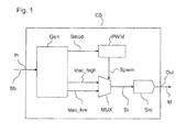
- FIG. 1 shows an exemplary embodiment of a current source according to the proposed principle.
- the current source CS comprises an input In for receiving a brightness signal Sb and an output Out for providing a driving current Id for at least one light-emitting diode, LED.
- the current source further comprises a generator circuit Gen, a pulse-width modulation, PWM, circuit, PMC, a multiplexing circuit MUX, and a current sourcing circuit Src.
- the generator circuit Gen is coupled to the input In and comprises outputs to provide a first and a second current value idac_high, idac_low and a duty cycle value Smod.
- the PWM circuit PMC is coupled to the generator circuit Gen.
- the PWM circuit PMC receives the duty cycle value Smod.
- the PWM circuit PMC comprises an output to provide a PWM signal Spwm as a function of the duty cycle value Smod.
- the multiplexing circuit MUX is coupled to the generator circuit Gen and to the PWM circuit PMC.
- the multiplexing circuit MUX comprises an output to provide a digital current signal Si.
- the current sourcing circuit Src is coupled to the output of the multiplexing circuit MUX.
- the current sourcing circuit Src is also coupled to the output Out of the current source.
- the brightness signal Sb is fed to the input In of the current source CS.
- the generator circuit Gen splits up the brightness signal Sb into most significant bits and least significant bits. The most significant bits are used for calculating the first and the second current values idac_high, idac_low. From the least significant bits the generator circuit Gen calculates the duty cycle value Smod.
- the duty cycle value Smod is used to generate the PWM signal Spwm by means of a saw-tooth signal and a comparator as well known by a person skilled in the art.
- the multiplexing circuit MUX switches between the first and the second current values idac_high, idac_low at its inputs in accordance with the PWM signal Spwm. By this, the multiplexing circuit MUX provides the digital current signal Si.
- the digital current signal Si is converted into the analog driving current Id in the current sourcing unit Src.
- the digital current signal Si is provided such that during 30% of the period length of the PWM signal Spwm the digital current signal Si has the value of the first current value idac_high and for the rest of the period, namely 70%, the digital current signal Si takes on the value of the second current value idac_low.
- the average of the driving current Id can be reduced. This results in a reduction of power consumption with still the same luminous intensity of an LED driven by the current source CS.
- FIG. 2A and Figure 2B each show diagrams corresponding to the embodiment of Figure 1 .
- the duty cycle value Smod is represented as a dotted zigzag curve
- the first current value idac_high is visualized as a thin full line step function
- the second current value idac_low is depicted as a thick full line step function.
- the values of the brightness signal Sb are depicted.
- the brightness signal Sb comprises 12 bits resulting in values starting from 0 to 4095, wherein 0 represents a dark LED and 4095 represents full brightness of the LED.
- the y-axis shows either the duty cycle value Smod wherein 0 corresponds to 0% and 4095 corresponds to 100% duty cycle.
- the y-axis depicts values of the first and second current values idac_high, idac_low, wherein 0 corresponds to 0 Milliampere and 2550 corresponds to 25,5 Milliampere.
- the brightness signal Sb is divided into various segments, each segment being characterized by a special value for the first current value idac_high and another slightly different value for the second current value idac_low.
- the duty cycle value Smod takes on a specific value curve for realizing the desired product of duty cycle and driving current as will be explained in more detail below in combination with Figures 4A and 4B .
- Figures 2A and 2B can be discerned in the range of values for the brightness signal Sb which are below 1000. At very low currents, the luminous intensity of LEDs can vary. Therefore, the first current value idac_high is set to a first minimum value Imin1 for this whole range which avoids operation at very low currents.
- the duty cycle value Smod is adapted accordingly.
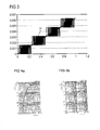
- Figure 3 shows another diagram corresponding to the embodiment of Figure 1 .
- the duty cycle value Smod are depicted on the x-axis.
- the duty cycle value is represented as a factor and not in percent.
- the black line represents the average value of the driving current Id.
- the oscillating curve represents values of the driving current Id.
- the driving current Id oscillates for each segment of the brightness signal Sb, or for the corresponding segment of the duty cycle value Smod between the first current value idac_high and the second current value idac_low.
- Figures 4A and 4B show diagrams of an LED.
- a typical white LED is used as an example.
- Figure 4A depicts the current If of an LED, also known as the forward current, in relation to the forward voltage Vf.
- Figure 4B presents the relative luminous intensity Iv in relation to the forward current If.
- the luminous intensity of the LED is approximately linear between 2 Milliampere and 20 Milliampere. From Figure 4A it can be discerned that a reduction of the forward current If by a factor of, for example, 10, reduces the forward voltage Vf by approximately 20%. At 20 mA of forward current If the forward voltage is 3.6 Volts. At 2 mA forward current If the forward voltage Vf is at 2.9 V.
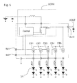
- FIG. 5 shows an exemplary embodiment of a driver circuit according to the proposed principle.
- the driver circuit comprises a voltage converter DCDC with an input for receiving a supply voltage VBat and with an output OutC to provide an output voltage Vout.
- the driver circuit further comprises at least one current source CS1 according to the proposed principle.
- the driver circuit comprises five current sources CS1, CS2, CS3, CS4 and CS5 which all conform to the proposed principle.
- Each current source CS1 to CS5 is connected to the output OutC of the voltage converter DCDC.
- An output of each of the current sources CS1 to CS5 forms an output LED1, LED2, LED3, LED4 and LED5 of the driver circuit.
- each output LED1, LED2, LED3, LED4 and LED5 at least one light-emitting diode D1 can be connected.
- Current sources CS1, CS2 and CS3 are controlled by a first brightness signal Sb1.
- Current sources CS4 and CS5 are controlled by a second brightness signal Sb2.
- Each of the current sources CS1 to CS5 provides a respective driving current Id1 to Id5 which is modulated according to the invented principle for the respectively connected LEDs.
Landscapes
- Led Devices (AREA)
- Circuit Arrangement For Electric Light Sources In General (AREA)
Abstract
Description
- The invention refers to the technical field of current sources.
- Current sources are used in various applications, for example for driving a light-emitting diode, LED. While LEDs are gaining importance because of their widespread use in backlights of mobile phones with liquid crystal displays, LCDs, current sources which control a luminous intensity of such LEDs are becoming a focal point for optimizing LED backlight.
- In a known implementation of such a current source for driving an LED, the intensity of the LED is controlled by means of a pulse-width modulation of the LED current provided by the current source. Thereby, a fixed current which is set by means of, for example, an external bias resistor is switched on and off according to a desired duty cycle with the help of a pulse-width modulated signal. The modulation frequency is high enough to avoid any flickering. The power consumption of the LED is proportional to a product of LED current, LED forward voltage and duty cycle of the pulse-width modulation signal. It can be desirable, especially in mobile phones, to reduce the power consumption of an LED.
- It is therefore an objective to provide an enhanced current source for this kind of application.
- This objective is achieved by the subject-matter of the independent patent claims. Embodiments and developments of the invention are subject-matter of the dependent claims.
- In one embodiment a current source comprises an input for receiving a brightness signal and an output for providing a driving current for at least one light-emitting diode. Thereby, the current source is configured to extract a first and a second current value from the brightness signal, to derive a duty cycle value from the brightness signal and to modulate the driving current as a function of the duty cycle value in a pulse-width modulation comprising the first and the second current values.
- The current source extracts the first and the second current values from the brightness signal. At the same time, the duty cycle value is derived from the brightness signal. The driving current is then generated by modulating between the first and the second current value according to the duty cycle value in a pulse-width modulation.
- As the driving current for the at least one LED is modulated between the first and the second current value, a reduced LED average current can be achieved by increasing the duty cycle value. This advantageously results in the same brightness of the LED with reduced forward voltage and reduced driving current, consequently with reduced power dissipation.
- The duty cycle is also known as "duty factor". It designates the ratio of the duration of an impulse to the duration of the total period of a pulse-width modulated signal.
- In another embodiment the brightness signal comprises a digital signal and is configured to control a brightness of the at least one LED.
- In a further embodiment the first and second current values are extracted from the brightness signal using a number of most significant bits.
- In another embodiment the duty cycle value is derived from the brightness signal using a number of least significant bits. The duty cycle value represents a value of the duty cycle of the driving current.
- The brightness signal is split up into two parts, namely the number of most significant bits and the number of least significant bits. The most significant bits are used for determining the first and second current values. The least significant bits are used to generate the duty cycle value.
- In another embodiment the brightness signal is divided into segments. For each segment the upper limit represents the first current value and the lower limit represents the second current value, respectively.
- This segmentation results in a step function in which a number of possible values of the brightness signal are grouped together in a segment with a fixed value for the first current value and a fixed value for the second current value for the whole segment.
- In a further development the first and the second current values each comprise a digital value and the first current value is different from the second current value.
- In a further embodiment the first current value is set to a first minimum value above zero. The second current value is set to a second minimum value above zero or zero.
- Consequently, the driving current is modulated between two different current values according to a duty cycle determined by the duty cycle value. As the luminous intensity of LEDs tends to vary at very low currents, first and second minimum values are used for first and second current values, respectively, to avoid operation at very low currents.
- In another embodiment the current source further comprises a generator circuit, a pulse-width modulation circuit, a multiplexing circuit and a current sourcing circuit. The generator circuit is coupled to the input and comprises outputs to provide the first and second current values and the duty cycle value. The pulse-width modulation, PWM, circuit is coupled to the generator circuit and comprises an output to provide a PWM signal as a function of the duty cycle value. The multiplexing circuit is coupled to the generator circuit and to the PWM circuit and comprises an output to provide a digital current signal as a function of the first and second current values and the PWM signal. The current sourcing unit is coupled to the multiplexing circuit and to the output and is configured to generate the driving current as a function of the digital current signal.
- The generator circuit splits up the brightness signal into most significant bits which are used for generating first and second current values and into least significant bits resulting in the duty cycle value. The PWM circuit generates the PWM signal that has a duty cycle corresponding to the duty cycle value. The multiplexing circuit switches between first and second current values using the PWM signal to control the switching. The current sourcing circuit provides the analog driving current in accordance with the digital current signal.
- In other words, the value of the digital current signal is first roughly determined by means of the first and second current values. Next, a fine-tuning of the digital current signal is completed by modulating between first and second current values according to the derived duty cycle value. The digital current signal is converted into the analog driving current.
- In a further development, the current sourcing circuit comprises at least one adjustable current source.
- The current sourcing circuit can also be realized by using a number n of standard weighted current sources. Each standard weighted current source provides a current of a distinct value. The number n of weighted current sources corresponds to the number n of bits implemented in the current sourcing circuit. As an additional effect, current spikes on an LED driven by the current source are reduced by 2 to the power of n. This reduces the generated electromagnetic radiation and voltage ripple on connected capacitors and possibly audible noise from capacitors.
- In one embodiment a driver circuit for light-emitting diodes comprises a voltage converter and at least one current source as described above. The voltage converter has an input for receiving a supply voltage and an output to provide an output voltage. The current source is connected to the output of the voltage converter. The output of the at least one current source forms an output of the driver circuit. This output is configured to be coupled to at least one LED. The at least one LED is driven by the driving current.
- The voltage converter converts the supply voltage to the output voltage which is used by the at least one current source to provide the driving current to the at least one LED.
- As the average of the driving current provided to the LED can be reduced and the duty cycle of the driving current is boosted by the same amount, the power consumption of the LED is reduced. Still the same luminous intensity of the LED is achieved. Light output is stable even at low current levels.
- The current source and driver circuit can be implemented with any kind of LED arrangement, e.g. series, parallel or a combination of both. For example, an array of 6x6 LEDs can also be powered by driver circuit.
- In one embodiment a method for providing a driving current comprises the following steps:
- receiving a brightness signal,
- generating a first and a second current value as a function of the brightness signal,
- generating a duty cycle value as a function the brightness signal, and
- providing a driving current as a function of a pulse-width modulation of the first and second current values with the duty cycle value.
- In a further embodiment providing the driving current comprises:
- generating a PWM signal as a function of the duty cycle value in a pulse-width modulation,
- generating a digital current signal by multiplexing the first and the second current values as a function of the PWM signal, and
- converting the digital current signal into the driving current.
- The text below explains the invention in detail using exemplary embodiments with reference to the drawings. Components and circuit elements that are functionally identical or have the identical effect bear identical reference numbers. In so far as circuit parts or components correspond to one another in function, a description of them will not be repeated in each of the following figures. Therein:
-
Figure 1 shows an exemplary embodiment of a current source according to the proposed principle, -
Figures 2A and 2B show diagrams corresponding to the embodiment ofFigure 1 , -
Figure 3 shows another diagram corresponding to the embodiment ofFigure 1 , -
Figures 4A and 4B show diagrams of an LED, and -
Figure 5 shows an exemplary embodiment of a driver circuit according to the proposed principle. -
Figure 1 shows an exemplary embodiment of a current source according to the proposed principle. The current source CS comprises an input In for receiving a brightness signal Sb and an output Out for providing a driving current Id for at least one light-emitting diode, LED. The current source further comprises a generator circuit Gen, a pulse-width modulation, PWM, circuit, PMC, a multiplexing circuit MUX, and a current sourcing circuit Src. The generator circuit Gen is coupled to the input In and comprises outputs to provide a first and a second current value idac_high, idac_low and a duty cycle value Smod. The PWM circuit PMC is coupled to the generator circuit Gen. The PWM circuit PMC receives the duty cycle value Smod. The PWM circuit PMC comprises an output to provide a PWM signal Spwm as a function of the duty cycle value Smod. The multiplexing circuit MUX is coupled to the generator circuit Gen and to the PWM circuit PMC. The multiplexing circuit MUX comprises an output to provide a digital current signal Si. The current sourcing circuit Src is coupled to the output of the multiplexing circuit MUX. The current sourcing circuit Src is also coupled to the output Out of the current source. - The brightness signal Sb is fed to the input In of the current source CS. The generator circuit Gen splits up the brightness signal Sb into most significant bits and least significant bits. The most significant bits are used for calculating the first and the second current values idac_high, idac_low. From the least significant bits the generator circuit Gen calculates the duty cycle value Smod. In the PMW circuit PMC the duty cycle value Smod is used to generate the PWM signal Spwm by means of a saw-tooth signal and a comparator as well known by a person skilled in the art. The multiplexing circuit MUX switches between the first and the second current values idac_high, idac_low at its inputs in accordance with the PWM signal Spwm. By this, the multiplexing circuit MUX provides the digital current signal Si. The digital current signal Si is converted into the analog driving current Id in the current sourcing unit Src.
- As an example for the multiplexing circuit MUX, if the duty cycle value Smod is at 30% or 0,3, the digital current signal Si is provided such that during 30% of the period length of the PWM signal Spwm the digital current signal Si has the value of the first current value idac_high and for the rest of the period, namely 70%, the digital current signal Si takes on the value of the second current value idac_low.
- Because of the modulation of the driving current Id with an adjustable duty cycle Smod, the average of the driving current Id can be reduced. This results in a reduction of power consumption with still the same luminous intensity of an LED driven by the current source CS.
-
Figure 2A and Figure 2B each show diagrams corresponding to the embodiment ofFigure 1 . In each case, the duty cycle value Smod is represented as a dotted zigzag curve, the first current value idac_high is visualized as a thin full line step function and the second current value idac_low is depicted as a thick full line step function. On the x-axis the values of the brightness signal Sb are depicted. In this example, the brightness signal Sb comprises 12 bits resulting in values starting from 0 to 4095, wherein 0 represents a dark LED and 4095 represents full brightness of the LED. The y-axis shows either the duty cycle value Smod wherein 0 corresponds to 0% and 4095 corresponds to 100% duty cycle. Or the y-axis depicts values of the first and second current values idac_high, idac_low, wherein 0 corresponds to 0 Milliampere and 2550 corresponds to 25,5 Milliampere. - Both figures show that the brightness signal Sb is divided into various segments, each segment being characterized by a special value for the first current value idac_high and another slightly different value for the second current value idac_low. For each segment the duty cycle value Smod takes on a specific value curve for realizing the desired product of duty cycle and driving current as will be explained in more detail below in combination with
Figures 4A and 4B . - The difference between
Figures 2A and 2B can be discerned in the range of values for the brightness signal Sb which are below 1000. At very low currents, the luminous intensity of LEDs can vary. Therefore, the first current value idac_high is set to a first minimum value Imin1 for this whole range which avoids operation at very low currents. The duty cycle value Smod is adapted accordingly. - By modulating the driving current Id between first and second current values idac_high, idac_low, high current spikes of the driving current Id are avoided.
-
Figure 3 shows another diagram corresponding to the embodiment ofFigure 1 . For readability reasons only a small section ofFigure 2A is shown here. On the x-axis values of the duty cycle value Smod are depicted. In this case, the duty cycle value is represented as a factor and not in percent. The black line represents the average value of the driving current Id. The oscillating curve represents values of the driving current Id. - It can be seen that the driving current Id oscillates for each segment of the brightness signal Sb, or for the corresponding segment of the duty cycle value Smod between the first current value idac_high and the second current value idac_low.
-
Figures 4A and 4B show diagrams of an LED. A typical white LED is used as an example.Figure 4A depicts the current If of an LED, also known as the forward current, in relation to the forward voltage Vf.Figure 4B presents the relative luminous intensity Iv in relation to the forward current If. - As can be seen, the luminous intensity of the LED is approximately linear between 2 Milliampere and 20 Milliampere. From
Figure 4A it can be discerned that a reduction of the forward current If by a factor of, for example, 10, reduces the forward voltage Vf by approximately 20%. At 20 mA of forward current If the forward voltage is 3.6 Volts. At 2 mA forward current If the forward voltage Vf is at 2.9 V. The power consumption of an LED is calculated according to the following equation:
in which P corresponds to the power consumption, D represents the value of the duty cycle, If represents the value of the forward current If and Vf corresponds to the value of the forward voltage Vf. - Regarding the example described above, this means that 20% of power can be saved when driving the LED with a driving current Id corresponding to a forward current If which is reduced by a factor of 10 and increasing the duty cycle by the same amount.
-
Figure 5 shows an exemplary embodiment of a driver circuit according to the proposed principle. The driver circuit comprises a voltage converter DCDC with an input for receiving a supply voltage VBat and with an output OutC to provide an output voltage Vout. The driver circuit further comprises at least one current source CS1 according to the proposed principle. In this example, the driver circuit comprises five current sources CS1, CS2, CS3, CS4 and CS5 which all conform to the proposed principle. Each current source CS1 to CS5 is connected to the output OutC of the voltage converter DCDC. An output of each of the current sources CS1 to CS5 forms an output LED1, LED2, LED3, LED4 and LED5 of the driver circuit. To each output LED1, LED2, LED3, LED4 and LED5 at least one light-emitting diode D1 can be connected. Current sources CS1, CS2 and CS3 are controlled by a first brightness signal Sb1. Current sources CS4 and CS5 are controlled by a second brightness signal Sb2. Each of the current sources CS1 to CS5 provides a respective driving current Id1 to Id5 which is modulated according to the invented principle for the respectively connected LEDs. -
- Sb, Sb1, Sb2
- brightness signal
- idac_high, idac_low
- current value
- Smod
- modulation value
- Spwm
- PWM signal
- Si
- digital current signal
- Id, Id1,..., Id5
- driving current
- Gen
- generator circuit
- PMC
- PWM circuit
- MUX
- multiplexing circuit
- Src
- current sourcing circuit
- CS, CS1,..., CS5
- current source
- DCDC
- voltage converter
- VBat
- supply voltage
- In
- input
- Out, OutC, LED1
- output
- Vout
- output voltage
- D1
- light-emitting diode
- Imin1
- minimum value
- LED1,..., LED5
- output
Claims (12)
- Current source, comprising- an input (In) for receiving a brightness signal (Sb),- an output (Out) for providing a driving current (Id) for at least one light-emitting diode, LED,
wherein the current source (CS) is configured- to extract a first and a second current value (idac_high, idac_low) from the brightness signal (Sb),- to derive a duty cycle value (Smod) from the brightness signal (Sb) and- to modulate the driving current (Id) as a function of the duty cycle value (Smod) in a pulse-width modulation comprising the first and the second current values (idac_high, idac_low). - Current source according to claim 1,
wherein the brightness signal (Sb) comprises a digital signal and is configured to control a brightness of the at least one LED. - Current source according to claim 1 or 2,
wherein the first and second current values (idac_high, idac_low) are extracted from the brightness signal (Sb) using a number of most significant bits. - Current source according to any of claims 1 to 3,
wherein the duty cycle value (Smod) is generated from the brightness signal (Sb) using a number of least significant bits, and
the duty cycle value (Smod) represents a value of a duty-cycle of the driving current (Id). - Current source according to any of claims 1 to 4,
wherein the brightness signal (Sb) is divided into segments, and wherein for each segment the upper limit represents the first current value (idac_high) and the lower limit represents the second current value (idac_low), respectively. - Current source according to any of claims 1 to 5,
wherein- the first and the second current values (idac_high, idac_low) each comprise a digital value, and- the first current value (idac_high) is different from the second current value (idac_low). - Current source according to any of claims 1 to 6,
wherein the first current value (idac_high) is set to a first minimum value (Imin1) above zero, and wherein the second current value (idac_low) is set to a second minimum value (Imin2) above zero or zero. - Current source according to any of claims 1 to 7, further comprising- a generator circuit (Gen) which is coupled to the input (In) and comprises outputs to provide the first and second current values (idac_high, idac_low) and the duty cycle value (Smod),- a pulse-width modulation, PWM, circuit (PWM) which is coupled to the generator circuit (Gen) and comprises an output to provide a PWM signal (Spwm) as a function of the duty cycle value (Smod),- a multiplexing circuit (MUX) which is coupled to the generator circuit (Gen) and to the PWM circuit (PWM) and comprises an output to provide a digital current signal (Si) as a function of the first and second current values (idac_high, idac_low) and the PWM signal (Spwm), and- a current sourcing circuit (Src) which is coupled to the multiplexing circuit (MUX) and the output (Out) and is configured to generate the driving current (Id) as a function of the digital current signal (Si).
- Current source according to claim 8,
wherein the current sourcing circuit (Src) comprises at least one adjustable current source. - Driver circuit for light-emitting diodes,
comprising- a voltage converter (DCDC) with an input for receiving a supply voltage (VBat) and with an output (OutC) to provide an output voltage (Vout),- at least one current source (CS1) according to one of claims 1 to 9, the current source (CS1) being connected to the output (OutC) of the voltage converter (DCDC), wherein the output (Out) of the at least one current source (CS1) forms an output (LED1) of the driver circuit and is configured to be coupled to at least one light-emitting diode (D1), the at least one light-emitting diode (D1) being driven by the driving current (Id1). - Method for providing a driving current comprising the following steps:- receiving a brightness signal (Sb),- generating a first and a second current value (idac_high, idac_low) as a function of the brightness signal (Sb),- generating a duty cycle value (Smod) as a function of the brightness signal (Sb),- providing a driving current (Id) as a function of a pulse-width modulation of the first and second current values (idac_high, idac_low) with the duty cycle value (Smod).
- Method according to claim 11,
wherein providing the driving current (Id) comprises- generating a PWM signal (Spwm) as a function of the duty cycle value (Smod) in a pulse-width modulation,- generating a digital current signal (Si) by multiplexing the first and second current values (idac_high, idac_low) as a function of the PWM signal (Spwm), and- converting the digital current signal (Si) into the driving current (Id).
Priority Applications (2)
| Application Number | Priority Date | Filing Date | Title |
|---|---|---|---|
| EP12166432.0A EP2661153B1 (en) | 2012-05-02 | 2012-05-02 | Current source and method for providing a driving current |
| US13/874,351 US9148914B2 (en) | 2012-05-02 | 2013-04-30 | Current source and method for providing a driving current |
Applications Claiming Priority (1)
| Application Number | Priority Date | Filing Date | Title |
|---|---|---|---|
| EP12166432.0A EP2661153B1 (en) | 2012-05-02 | 2012-05-02 | Current source and method for providing a driving current |
Publications (2)
| Publication Number | Publication Date |
|---|---|
| EP2661153A1 true EP2661153A1 (en) | 2013-11-06 |
| EP2661153B1 EP2661153B1 (en) | 2019-11-06 |
Family
ID=46049269
Family Applications (1)
| Application Number | Title | Priority Date | Filing Date |
|---|---|---|---|
| EP12166432.0A Active EP2661153B1 (en) | 2012-05-02 | 2012-05-02 | Current source and method for providing a driving current |
Country Status (2)
| Country | Link |
|---|---|
| US (1) | US9148914B2 (en) |
| EP (1) | EP2661153B1 (en) |
Cited By (2)
| Publication number | Priority date | Publication date | Assignee | Title |
|---|---|---|---|---|
| DE102013108257B4 (en) * | 2013-08-01 | 2019-10-31 | Technische Universität Dresden | Method and device for dimming LED |
| DE102015203781B4 (en) * | 2014-08-28 | 2021-03-18 | Dialog Semiconductor (Uk) Limited | Non-linear current IDAC with synthesis in time domain |
Families Citing this family (4)
| Publication number | Priority date | Publication date | Assignee | Title |
|---|---|---|---|---|
| KR102285264B1 (en) * | 2015-02-10 | 2021-08-04 | 삼성전자주식회사 | Display apparatus and method for driving backlight |
| US10395584B2 (en) | 2016-11-22 | 2019-08-27 | Planar Systems, Inc. | Intensity scaled dithering pulse width modulation |
| CN115810327B (en) * | 2021-09-13 | 2025-05-23 | 西安青松光电技术有限公司 | Display method of LED display screen, storage medium and electronic equipment |
| US11688333B1 (en) | 2021-12-30 | 2023-06-27 | Microsoft Technology Licensing, Llc | Micro-LED display |
Citations (7)
| Publication number | Priority date | Publication date | Assignee | Title |
|---|---|---|---|---|
| US5671003A (en) * | 1991-11-04 | 1997-09-23 | Eastman Kodak Company | Hybrid digital image printer with halftone gray scale capability |
| WO2001073818A1 (en) * | 2000-03-31 | 2001-10-04 | Hong Sam Pyo | Light emitting lamp |
| DE102006032071A1 (en) * | 2006-07-11 | 2008-01-17 | Austriamicrosystems Ag | Control circuit and method for controlling light emitting diodes |
| US20090079360A1 (en) * | 2007-09-21 | 2009-03-26 | Exclara Inc. | System and Method for Regulation of Solid State Lighting |
| GB2454557A (en) * | 2007-11-09 | 2009-05-13 | Diehl Aerospace Gmbh | Generating mixed light colours |
| US20090303161A1 (en) * | 2008-06-06 | 2009-12-10 | Neil Messmer | Apparatus and methods for driving solid-state illumination sources |
| WO2011135505A1 (en) * | 2010-04-30 | 2011-11-03 | Koninklijke Philips Electronics N.V. | Dimming regulator including programmable hysteretic down-converter for increasing dimming resolution of solid state lighting loads |
Family Cites Families (12)
| Publication number | Priority date | Publication date | Assignee | Title |
|---|---|---|---|---|
| JP2001308710A (en) * | 2000-04-21 | 2001-11-02 | Sony Corp | Modulation circuit, image display device using the same, and modulation method |
| DE102004003698B4 (en) * | 2004-01-24 | 2005-11-24 | Preh Gmbh | Circuit arrangement for controlling bulbs |
| US7145295B1 (en) * | 2005-07-24 | 2006-12-05 | Aimtron Technology Corp. | Dimming control circuit for light-emitting diodes |
| US7642725B2 (en) * | 2005-11-17 | 2010-01-05 | Texas Instruments Incorporated | Unbalanced plural string LED driver with common return resistor |
| CN1909758B (en) * | 2006-08-18 | 2012-11-28 | 北京中星微电子有限公司 | Multifunctional driving controller |
| TWI359317B (en) * | 2007-10-30 | 2012-03-01 | Au Optronics Corp | Backlight control device and method for controllin |
| US20110199011A1 (en) * | 2009-01-09 | 2011-08-18 | Ken Nakazawa | Light-emitting diode driving circuit and planar illuminating device having same |
| CN101814270B (en) * | 2009-02-20 | 2012-08-22 | 国琏电子(上海)有限公司 | Backlight drive system |
| KR101578214B1 (en) * | 2009-08-04 | 2015-12-16 | 엘지디스플레이 주식회사 | Liquid crystal display and driving method thereof |
| JP4922439B2 (en) * | 2010-07-01 | 2012-04-25 | シャープ株式会社 | LED control device, liquid crystal display device |
| CN102014543B (en) * | 2010-07-02 | 2011-12-28 | 凹凸电子(武汉)有限公司 | Drive circuit and method of drive light source and controller |
| US8587212B2 (en) * | 2010-08-10 | 2013-11-19 | Industrial Technology Research Institute | Lighting system, dimming control apparatus and dimming control method |
-
2012
- 2012-05-02 EP EP12166432.0A patent/EP2661153B1/en active Active
-
2013
- 2013-04-30 US US13/874,351 patent/US9148914B2/en not_active Expired - Fee Related
Patent Citations (7)
| Publication number | Priority date | Publication date | Assignee | Title |
|---|---|---|---|---|
| US5671003A (en) * | 1991-11-04 | 1997-09-23 | Eastman Kodak Company | Hybrid digital image printer with halftone gray scale capability |
| WO2001073818A1 (en) * | 2000-03-31 | 2001-10-04 | Hong Sam Pyo | Light emitting lamp |
| DE102006032071A1 (en) * | 2006-07-11 | 2008-01-17 | Austriamicrosystems Ag | Control circuit and method for controlling light emitting diodes |
| US20090079360A1 (en) * | 2007-09-21 | 2009-03-26 | Exclara Inc. | System and Method for Regulation of Solid State Lighting |
| GB2454557A (en) * | 2007-11-09 | 2009-05-13 | Diehl Aerospace Gmbh | Generating mixed light colours |
| US20090303161A1 (en) * | 2008-06-06 | 2009-12-10 | Neil Messmer | Apparatus and methods for driving solid-state illumination sources |
| WO2011135505A1 (en) * | 2010-04-30 | 2011-11-03 | Koninklijke Philips Electronics N.V. | Dimming regulator including programmable hysteretic down-converter for increasing dimming resolution of solid state lighting loads |
Cited By (2)
| Publication number | Priority date | Publication date | Assignee | Title |
|---|---|---|---|---|
| DE102013108257B4 (en) * | 2013-08-01 | 2019-10-31 | Technische Universität Dresden | Method and device for dimming LED |
| DE102015203781B4 (en) * | 2014-08-28 | 2021-03-18 | Dialog Semiconductor (Uk) Limited | Non-linear current IDAC with synthesis in time domain |
Also Published As
| Publication number | Publication date |
|---|---|
| EP2661153B1 (en) | 2019-11-06 |
| US9148914B2 (en) | 2015-09-29 |
| US20130293140A1 (en) | 2013-11-07 |
Similar Documents
| Publication | Publication Date | Title |
|---|---|---|
| EP2661153B1 (en) | Current source and method for providing a driving current | |
| US9386661B2 (en) | Driver circuit and method for driving an electrical load | |
| EP2168118B1 (en) | Driving circuit for driving a plurality of light sources arranged in a series configuration | |
| KR101009049B1 (en) | LED lighting device | |
| JP3755770B2 (en) | Load drive device and portable device | |
| US20100109550A1 (en) | LED Dimming Techniques Using Spread Spectrum Modulation | |
| EP1689212A1 (en) | Method and system for dimming light sources | |
| EP2364064A2 (en) | LED lighting device | |
| EP2793534A1 (en) | Led driving device | |
| EP2680669A1 (en) | Light emitting diode driving apparatus, driving method of light emitting diode, and computer-readable recording medium | |
| US8796957B2 (en) | Multi-string LED driving method and system | |
| KR20090051236A (en) | PMB method and apparatus, and light source driven by it | |
| TWI426822B (en) | Digital dimming device and digital dimming method | |
| US7496297B2 (en) | LED system for illumination and data transmission | |
| EP1649729B1 (en) | Method and device for supplying power to leds | |
| US20150245431A1 (en) | Driver device and driving method for driving a load, in particular an led unit | |
| US10652981B1 (en) | Method for driving a plurality of light emitting diodes and drive circuit | |
| EP2911475A1 (en) | PDM modulation of LED current | |
| EP2434839A1 (en) | Driving circuit for light emitting elements | |
| CN102026440A (en) | Driving device and lighting device | |
| US12452976B2 (en) | Light source driver | |
| JP6659551B2 (en) | Light emitting diode drive based on ripple | |
| US9572207B2 (en) | Dimming range extension | |
| KR102103798B1 (en) | Method of driving light-source, light-source apparatus for performing the method and display apparatus having the light-source apparatus | |
| KR20130135487A (en) | Method of driving light-source, light-source apparatus for performing the method and display apparatus having the light-source apparatus |
Legal Events
| Date | Code | Title | Description |
|---|---|---|---|
| PUAI | Public reference made under article 153(3) epc to a published international application that has entered the european phase |
Free format text: ORIGINAL CODE: 0009012 |
|
| AK | Designated contracting states |
Kind code of ref document: A1 Designated state(s): AL AT BE BG CH CY CZ DE DK EE ES FI FR GB GR HR HU IE IS IT LI LT LU LV MC MK MT NL NO PL PT RO RS SE SI SK SM TR |
|
| AX | Request for extension of the european patent |
Extension state: BA ME |
|
| 17P | Request for examination filed |
Effective date: 20140505 |
|
| RBV | Designated contracting states (corrected) |
Designated state(s): AL AT BE BG CH CY CZ DE DK EE ES FI FR GB GR HR HU IE IS IT LI LT LU LV MC MK MT NL NO PL PT RO RS SE SI SK SM TR |
|
| STAA | Information on the status of an ep patent application or granted ep patent |
Free format text: STATUS: EXAMINATION IS IN PROGRESS |
|
| 17Q | First examination report despatched |
Effective date: 20170712 |
|
| GRAP | Despatch of communication of intention to grant a patent |
Free format text: ORIGINAL CODE: EPIDOSNIGR1 |
|
| STAA | Information on the status of an ep patent application or granted ep patent |
Free format text: STATUS: GRANT OF PATENT IS INTENDED |
|
| INTG | Intention to grant announced |
Effective date: 20190405 |
|
| GRAS | Grant fee paid |
Free format text: ORIGINAL CODE: EPIDOSNIGR3 |
|
| GRAJ | Information related to disapproval of communication of intention to grant by the applicant or resumption of examination proceedings by the epo deleted |
Free format text: ORIGINAL CODE: EPIDOSDIGR1 |
|
| GRAL | Information related to payment of fee for publishing/printing deleted |
Free format text: ORIGINAL CODE: EPIDOSDIGR3 |
|
| STAA | Information on the status of an ep patent application or granted ep patent |
Free format text: STATUS: EXAMINATION IS IN PROGRESS |
|
| INTC | Intention to grant announced (deleted) | ||
| RAP1 | Party data changed (applicant data changed or rights of an application transferred) |
Owner name: AMS AG |
|
| RIN1 | Information on inventor provided before grant (corrected) |
Inventor name: TRATTLER, PETER Inventor name: BOEHM, MICHAEL Inventor name: MANNINGER, MARIO |
|
| RAP1 | Party data changed (applicant data changed or rights of an application transferred) |
Owner name: AMS AG |
|
| RIN1 | Information on inventor provided before grant (corrected) |
Inventor name: MANNINGER, MARIO Inventor name: BOEHM, MICHAEL Inventor name: TRATTLER, PETER |
|
| GRAR | Information related to intention to grant a patent recorded |
Free format text: ORIGINAL CODE: EPIDOSNIGR71 |
|
| STAA | Information on the status of an ep patent application or granted ep patent |
Free format text: STATUS: GRANT OF PATENT IS INTENDED |
|
| GRAA | (expected) grant |
Free format text: ORIGINAL CODE: 0009210 |
|
| STAA | Information on the status of an ep patent application or granted ep patent |
Free format text: STATUS: THE PATENT HAS BEEN GRANTED |
|
| AK | Designated contracting states |
Kind code of ref document: B1 Designated state(s): AL AT BE BG CH CY CZ DE DK EE ES FI FR GB GR HR HU IE IS IT LI LT LU LV MC MK MT NL NO PL PT RO RS SE SI SK SM TR |
|
| INTG | Intention to grant announced |
Effective date: 20190927 |
|
| REG | Reference to a national code |
Ref country code: GB Ref legal event code: FG4D |
|
| REG | Reference to a national code |
Ref country code: CH Ref legal event code: EP Ref country code: AT Ref legal event code: REF Ref document number: 1200668 Country of ref document: AT Kind code of ref document: T Effective date: 20191115 |
|
| REG | Reference to a national code |
Ref country code: DE Ref legal event code: R079 Ref document number: 602012065382 Country of ref document: DE Free format text: PREVIOUS MAIN CLASS: H05B0033080000 Ipc: H05B0045000000 |
|
| REG | Reference to a national code |
Ref country code: IE Ref legal event code: FG4D |
|
| REG | Reference to a national code |
Ref country code: DE Ref legal event code: R096 Ref document number: 602012065382 Country of ref document: DE |
|
| REG | Reference to a national code |
Ref country code: NL Ref legal event code: MP Effective date: 20191106 |
|
| REG | Reference to a national code |
Ref country code: LT Ref legal event code: MG4D |
|
| PG25 | Lapsed in a contracting state [announced via postgrant information from national office to epo] |
Ref country code: ES Free format text: LAPSE BECAUSE OF FAILURE TO SUBMIT A TRANSLATION OF THE DESCRIPTION OR TO PAY THE FEE WITHIN THE PRESCRIBED TIME-LIMIT Effective date: 20191106 Ref country code: PT Free format text: LAPSE BECAUSE OF FAILURE TO SUBMIT A TRANSLATION OF THE DESCRIPTION OR TO PAY THE FEE WITHIN THE PRESCRIBED TIME-LIMIT Effective date: 20200306 Ref country code: LT Free format text: LAPSE BECAUSE OF FAILURE TO SUBMIT A TRANSLATION OF THE DESCRIPTION OR TO PAY THE FEE WITHIN THE PRESCRIBED TIME-LIMIT Effective date: 20191106 Ref country code: NL Free format text: LAPSE BECAUSE OF FAILURE TO SUBMIT A TRANSLATION OF THE DESCRIPTION OR TO PAY THE FEE WITHIN THE PRESCRIBED TIME-LIMIT Effective date: 20191106 Ref country code: FI Free format text: LAPSE BECAUSE OF FAILURE TO SUBMIT A TRANSLATION OF THE DESCRIPTION OR TO PAY THE FEE WITHIN THE PRESCRIBED TIME-LIMIT Effective date: 20191106 Ref country code: BG Free format text: LAPSE BECAUSE OF FAILURE TO SUBMIT A TRANSLATION OF THE DESCRIPTION OR TO PAY THE FEE WITHIN THE PRESCRIBED TIME-LIMIT Effective date: 20200206 Ref country code: NO Free format text: LAPSE BECAUSE OF FAILURE TO SUBMIT A TRANSLATION OF THE DESCRIPTION OR TO PAY THE FEE WITHIN THE PRESCRIBED TIME-LIMIT Effective date: 20200206 Ref country code: PL Free format text: LAPSE BECAUSE OF FAILURE TO SUBMIT A TRANSLATION OF THE DESCRIPTION OR TO PAY THE FEE WITHIN THE PRESCRIBED TIME-LIMIT Effective date: 20191106 Ref country code: GR Free format text: LAPSE BECAUSE OF FAILURE TO SUBMIT A TRANSLATION OF THE DESCRIPTION OR TO PAY THE FEE WITHIN THE PRESCRIBED TIME-LIMIT Effective date: 20200207 Ref country code: LV Free format text: LAPSE BECAUSE OF FAILURE TO SUBMIT A TRANSLATION OF THE DESCRIPTION OR TO PAY THE FEE WITHIN THE PRESCRIBED TIME-LIMIT Effective date: 20191106 Ref country code: SE Free format text: LAPSE BECAUSE OF FAILURE TO SUBMIT A TRANSLATION OF THE DESCRIPTION OR TO PAY THE FEE WITHIN THE PRESCRIBED TIME-LIMIT Effective date: 20191106 |
|
| PG25 | Lapsed in a contracting state [announced via postgrant information from national office to epo] |
Ref country code: HR Free format text: LAPSE BECAUSE OF FAILURE TO SUBMIT A TRANSLATION OF THE DESCRIPTION OR TO PAY THE FEE WITHIN THE PRESCRIBED TIME-LIMIT Effective date: 20191106 Ref country code: RS Free format text: LAPSE BECAUSE OF FAILURE TO SUBMIT A TRANSLATION OF THE DESCRIPTION OR TO PAY THE FEE WITHIN THE PRESCRIBED TIME-LIMIT Effective date: 20191106 Ref country code: IS Free format text: LAPSE BECAUSE OF FAILURE TO SUBMIT A TRANSLATION OF THE DESCRIPTION OR TO PAY THE FEE WITHIN THE PRESCRIBED TIME-LIMIT Effective date: 20200306 |
|
| PG25 | Lapsed in a contracting state [announced via postgrant information from national office to epo] |
Ref country code: AL Free format text: LAPSE BECAUSE OF FAILURE TO SUBMIT A TRANSLATION OF THE DESCRIPTION OR TO PAY THE FEE WITHIN THE PRESCRIBED TIME-LIMIT Effective date: 20191106 |
|
| PG25 | Lapsed in a contracting state [announced via postgrant information from national office to epo] |
Ref country code: RO Free format text: LAPSE BECAUSE OF FAILURE TO SUBMIT A TRANSLATION OF THE DESCRIPTION OR TO PAY THE FEE WITHIN THE PRESCRIBED TIME-LIMIT Effective date: 20191106 Ref country code: DK Free format text: LAPSE BECAUSE OF FAILURE TO SUBMIT A TRANSLATION OF THE DESCRIPTION OR TO PAY THE FEE WITHIN THE PRESCRIBED TIME-LIMIT Effective date: 20191106 Ref country code: EE Free format text: LAPSE BECAUSE OF FAILURE TO SUBMIT A TRANSLATION OF THE DESCRIPTION OR TO PAY THE FEE WITHIN THE PRESCRIBED TIME-LIMIT Effective date: 20191106 Ref country code: CZ Free format text: LAPSE BECAUSE OF FAILURE TO SUBMIT A TRANSLATION OF THE DESCRIPTION OR TO PAY THE FEE WITHIN THE PRESCRIBED TIME-LIMIT Effective date: 20191106 |
|
| REG | Reference to a national code |
Ref country code: DE Ref legal event code: R097 Ref document number: 602012065382 Country of ref document: DE |
|
| REG | Reference to a national code |
Ref country code: AT Ref legal event code: MK05 Ref document number: 1200668 Country of ref document: AT Kind code of ref document: T Effective date: 20191106 |
|
| PG25 | Lapsed in a contracting state [announced via postgrant information from national office to epo] |
Ref country code: SM Free format text: LAPSE BECAUSE OF FAILURE TO SUBMIT A TRANSLATION OF THE DESCRIPTION OR TO PAY THE FEE WITHIN THE PRESCRIBED TIME-LIMIT Effective date: 20191106 Ref country code: SK Free format text: LAPSE BECAUSE OF FAILURE TO SUBMIT A TRANSLATION OF THE DESCRIPTION OR TO PAY THE FEE WITHIN THE PRESCRIBED TIME-LIMIT Effective date: 20191106 |
|
| PLBE | No opposition filed within time limit |
Free format text: ORIGINAL CODE: 0009261 |
|
| STAA | Information on the status of an ep patent application or granted ep patent |
Free format text: STATUS: NO OPPOSITION FILED WITHIN TIME LIMIT |
|
| 26N | No opposition filed |
Effective date: 20200807 |
|
| PG25 | Lapsed in a contracting state [announced via postgrant information from national office to epo] |
Ref country code: SI Free format text: LAPSE BECAUSE OF FAILURE TO SUBMIT A TRANSLATION OF THE DESCRIPTION OR TO PAY THE FEE WITHIN THE PRESCRIBED TIME-LIMIT Effective date: 20191106 Ref country code: AT Free format text: LAPSE BECAUSE OF FAILURE TO SUBMIT A TRANSLATION OF THE DESCRIPTION OR TO PAY THE FEE WITHIN THE PRESCRIBED TIME-LIMIT Effective date: 20191106 |
|
| PG25 | Lapsed in a contracting state [announced via postgrant information from national office to epo] |
Ref country code: CH Free format text: LAPSE BECAUSE OF NON-PAYMENT OF DUE FEES Effective date: 20200531 Ref country code: LI Free format text: LAPSE BECAUSE OF NON-PAYMENT OF DUE FEES Effective date: 20200531 Ref country code: MC Free format text: LAPSE BECAUSE OF FAILURE TO SUBMIT A TRANSLATION OF THE DESCRIPTION OR TO PAY THE FEE WITHIN THE PRESCRIBED TIME-LIMIT Effective date: 20191106 Ref country code: IT Free format text: LAPSE BECAUSE OF FAILURE TO SUBMIT A TRANSLATION OF THE DESCRIPTION OR TO PAY THE FEE WITHIN THE PRESCRIBED TIME-LIMIT Effective date: 20191106 |
|
| REG | Reference to a national code |
Ref country code: BE Ref legal event code: MM Effective date: 20200531 |
|
| GBPC | Gb: european patent ceased through non-payment of renewal fee |
Effective date: 20200502 |
|
| PG25 | Lapsed in a contracting state [announced via postgrant information from national office to epo] |
Ref country code: LU Free format text: LAPSE BECAUSE OF NON-PAYMENT OF DUE FEES Effective date: 20200502 |
|
| PG25 | Lapsed in a contracting state [announced via postgrant information from national office to epo] |
Ref country code: IE Free format text: LAPSE BECAUSE OF NON-PAYMENT OF DUE FEES Effective date: 20200502 Ref country code: GB Free format text: LAPSE BECAUSE OF NON-PAYMENT OF DUE FEES Effective date: 20200502 Ref country code: FR Free format text: LAPSE BECAUSE OF NON-PAYMENT OF DUE FEES Effective date: 20200531 |
|
| PG25 | Lapsed in a contracting state [announced via postgrant information from national office to epo] |
Ref country code: BE Free format text: LAPSE BECAUSE OF NON-PAYMENT OF DUE FEES Effective date: 20200531 |
|
| PG25 | Lapsed in a contracting state [announced via postgrant information from national office to epo] |
Ref country code: TR Free format text: LAPSE BECAUSE OF FAILURE TO SUBMIT A TRANSLATION OF THE DESCRIPTION OR TO PAY THE FEE WITHIN THE PRESCRIBED TIME-LIMIT Effective date: 20191106 Ref country code: MT Free format text: LAPSE BECAUSE OF FAILURE TO SUBMIT A TRANSLATION OF THE DESCRIPTION OR TO PAY THE FEE WITHIN THE PRESCRIBED TIME-LIMIT Effective date: 20191106 Ref country code: CY Free format text: LAPSE BECAUSE OF FAILURE TO SUBMIT A TRANSLATION OF THE DESCRIPTION OR TO PAY THE FEE WITHIN THE PRESCRIBED TIME-LIMIT Effective date: 20191106 |
|
| PG25 | Lapsed in a contracting state [announced via postgrant information from national office to epo] |
Ref country code: MK Free format text: LAPSE BECAUSE OF FAILURE TO SUBMIT A TRANSLATION OF THE DESCRIPTION OR TO PAY THE FEE WITHIN THE PRESCRIBED TIME-LIMIT Effective date: 20191106 |
|
| PGFP | Annual fee paid to national office [announced via postgrant information from national office to epo] |
Ref country code: DE Payment date: 20220519 Year of fee payment: 11 |
|
| P01 | Opt-out of the competence of the unified patent court (upc) registered |
Effective date: 20230822 |
|
| REG | Reference to a national code |
Ref country code: DE Ref legal event code: R119 Ref document number: 602012065382 Country of ref document: DE |
|
| PG25 | Lapsed in a contracting state [announced via postgrant information from national office to epo] |
Ref country code: DE Free format text: LAPSE BECAUSE OF NON-PAYMENT OF DUE FEES Effective date: 20231201 |