EP2658198B1 - Verfahren zum empfangen eines frequenzdomänen-multiplexsignals und vorrichtung zum empfangen eines frequenzdomänen-multiplexsignals - Google Patents
Verfahren zum empfangen eines frequenzdomänen-multiplexsignals und vorrichtung zum empfangen eines frequenzdomänen-multiplexsignals Download PDFInfo
- Publication number
- EP2658198B1 EP2658198B1 EP13177394.7A EP13177394A EP2658198B1 EP 2658198 B1 EP2658198 B1 EP 2658198B1 EP 13177394 A EP13177394 A EP 13177394A EP 2658198 B1 EP2658198 B1 EP 2658198B1
- Authority
- EP
- European Patent Office
- Prior art keywords
- frequency
- signals
- signal
- fourier transform
- equalization
- Prior art date
- Legal status (The legal status is an assumption and is not a legal conclusion. Google has not performed a legal analysis and makes no representation as to the accuracy of the status listed.)
- Active
Links
- 238000000034 method Methods 0.000 title claims description 40
- 108010076504 Protein Sorting Signals Proteins 0.000 claims description 36
- 230000003287 optical effect Effects 0.000 claims description 14
- 239000006185 dispersion Substances 0.000 claims description 4
- 238000013459 approach Methods 0.000 claims description 2
- 230000010287 polarization Effects 0.000 description 28
- 238000004891 communication Methods 0.000 description 24
- 238000010586 diagram Methods 0.000 description 23
- 238000012545 processing Methods 0.000 description 23
- 238000005070 sampling Methods 0.000 description 17
- 238000004364 calculation method Methods 0.000 description 16
- 230000005540 biological transmission Effects 0.000 description 8
- 230000000694 effects Effects 0.000 description 5
- 238000001514 detection method Methods 0.000 description 4
- 238000005259 measurement Methods 0.000 description 4
- 230000001360 synchronised effect Effects 0.000 description 4
- 238000001228 spectrum Methods 0.000 description 3
- 230000006866 deterioration Effects 0.000 description 2
- 230000010363 phase shift Effects 0.000 description 2
- 230000001131 transforming effect Effects 0.000 description 2
- 238000012952 Resampling Methods 0.000 description 1
- 230000003044 adaptive effect Effects 0.000 description 1
- 239000000969 carrier Substances 0.000 description 1
- 230000015556 catabolic process Effects 0.000 description 1
- 238000006731 degradation reaction Methods 0.000 description 1
- 238000005562 fading Methods 0.000 description 1
- 238000003780 insertion Methods 0.000 description 1
- 230000037431 insertion Effects 0.000 description 1
- 239000013307 optical fiber Substances 0.000 description 1
- 238000000926 separation method Methods 0.000 description 1
- 230000008054 signal transmission Effects 0.000 description 1
Images

Classifications
-
- H—ELECTRICITY
- H04—ELECTRIC COMMUNICATION TECHNIQUE
- H04L—TRANSMISSION OF DIGITAL INFORMATION, e.g. TELEGRAPHIC COMMUNICATION
- H04L27/00—Modulated-carrier systems
- H04L27/26—Systems using multi-frequency codes
- H04L27/2601—Multicarrier modulation systems
- H04L27/2647—Arrangements specific to the receiver only
- H04L27/2655—Synchronisation arrangements
- H04L27/2668—Details of algorithms
- H04L27/2669—Details of algorithms characterised by the domain of operation
- H04L27/2672—Frequency domain
-
- H—ELECTRICITY
- H04—ELECTRIC COMMUNICATION TECHNIQUE
- H04L—TRANSMISSION OF DIGITAL INFORMATION, e.g. TELEGRAPHIC COMMUNICATION
- H04L25/00—Baseband systems
- H04L25/02—Details ; arrangements for supplying electrical power along data transmission lines
- H04L25/03—Shaping networks in transmitter or receiver, e.g. adaptive shaping networks
- H04L25/03006—Arrangements for removing intersymbol interference
- H04L25/03159—Arrangements for removing intersymbol interference operating in the frequency domain
-
- H—ELECTRICITY
- H04—ELECTRIC COMMUNICATION TECHNIQUE
- H04L—TRANSMISSION OF DIGITAL INFORMATION, e.g. TELEGRAPHIC COMMUNICATION
- H04L27/00—Modulated-carrier systems
- H04L27/26—Systems using multi-frequency codes
- H04L27/2601—Multicarrier modulation systems
- H04L27/2647—Arrangements specific to the receiver only
- H04L27/2649—Demodulators
- H04L27/265—Fourier transform demodulators, e.g. fast Fourier transform [FFT] or discrete Fourier transform [DFT] demodulators
- H04L27/26522—Fourier transform demodulators, e.g. fast Fourier transform [FFT] or discrete Fourier transform [DFT] demodulators using partial FFTs
-
- H—ELECTRICITY
- H04—ELECTRIC COMMUNICATION TECHNIQUE
- H04L—TRANSMISSION OF DIGITAL INFORMATION, e.g. TELEGRAPHIC COMMUNICATION
- H04L27/00—Modulated-carrier systems
- H04L27/26—Systems using multi-frequency codes
- H04L27/2601—Multicarrier modulation systems
- H04L27/2647—Arrangements specific to the receiver only
- H04L27/2655—Synchronisation arrangements
- H04L27/2657—Carrier synchronisation
- H04L27/266—Fine or fractional frequency offset determination and synchronisation
-
- H—ELECTRICITY
- H04—ELECTRIC COMMUNICATION TECHNIQUE
- H04L—TRANSMISSION OF DIGITAL INFORMATION, e.g. TELEGRAPHIC COMMUNICATION
- H04L25/00—Baseband systems
- H04L25/02—Details ; arrangements for supplying electrical power along data transmission lines
- H04L25/03—Shaping networks in transmitter or receiver, e.g. adaptive shaping networks
- H04L25/03006—Arrangements for removing intersymbol interference
- H04L2025/0335—Arrangements for removing intersymbol interference characterised by the type of transmission
- H04L2025/03375—Passband transmission
- H04L2025/03414—Multicarrier
Definitions
- the present invention relates to a method for receiving frequency domain multiplexed signals and a device for receiving frequency domain multiplexed signals in a communication system in which signals are multiplexed in the frequency domain.
- the present invention relates to a method for receiving frequency domain multiplexed signals and a device for receiving frequency domain multiplexed signals in which received signals that have been multiplexed in the frequency domain are equalized without applying a discrete Fourier transform.
- Orthogonal frequency division multiplexing system Orthogonal Frequency Division Multiplexing
- OFDM Orthogonal Frequency Division Multiplexing
- the sampling frequency of an analog to digital converter for discretizing received signals can be set to a frequency lower than a frequency of twice the baud rate of the received signals. Therefore, for example in a wireless LAN (Local Area Network) applied to IEEE802.11a, it is known that a band of approximately 16.6 MHz in a signal band of 20 MHz (megahertz) is used for data signals.
- ADC Analog Digital Converter
- an ADC in single carrier transmission, an ADC is required that can be adapted to a sampling frequency of approximately twice the frequency band of a signal. Therefore the advantage of being able to set a frequency lower than the frequency of twice the baud rate in OFDM is that signals can be transmitted efficiently by an ADC with a low sampling frequency, especially in optical communication in which the application is limited by the sampling frequency of the ADC and high frequency wireless communication.
- a frequency channel number of approximately 64 to 1024 is selected.
- the frequency at a receiving device is "0", that is, it has a frequency channel corresponding to a DC component. In a frequency channel corresponding to a DC component, the characteristics deteriorate due to the influence of interference between signals and noise. Therefore, frequency channels corresponding to these are not generally used.
- FDM Frequency Division Multiplexing
- OFDM Orthogonal Frequency Division Multiplexing
- US 2005/157782 concerns a method of communicating over a wideband communication channel divided into a plurality of sub-channels.
- a single serial message intended for one communication device is divided into a plurality of parallel messages.
- Each parallel message is encoded onto at least some sub-channels and is transmitted to the communication device over the wideband communication channel.
- US 2004/086027 concerns orthogonal superposition coding for direct-sequence communications. This document relates to a multicarrier spread-spectrum protocol for wireless and waveguide communications.
- a large number of frequency channel numbers cannot be set.
- the number of frequency channels in the OFDM contained in the frequency band of the received signal becomes lower due to the influence of the filter.
- a two carrier OFDM signal is received in which a signal with a transmission symbol rate of 5 Gbaud (gigabaud) is multiplexed into two frequency bands.
- the gap I between adjacent frequency channels is 5 GHz (gigahertz).
- the application of a discrete Fourier transform to the received signal will be considered.
- a discrete Fourier transform is a transform whereby a signal in the time domain is converted into a signal in the frequency domain. If a discrete Fourier transform of four points (central frequencies: ⁇ 2.5 GHz, ⁇ 5 GHz) is applied, signal domains corresponding to two frequency channels can be obtained.
- reference symbol C1 indicates the central frequency of signal channel 1
- reference symbol C2 indicates the central frequency of signal channel 2.
- Reference symbol P indicates the frequency band to which four frequency channels of a conventional Fourier transform correspond.
- a transmitting device that generates a transmitted signal and a receiving device that receives the signal transmitted as a received signal are connected to different reference signal generators.
- the receiving device if the frequency deviates, the signal quality deteriorates due to signals leaking in from adjacent frequency channels.
- the frequency deviation generated between a laser light used for transmission and a laser light used for reception is great, so that such a problem is likely to occur.
- a conventional receiving device 190 is shown in FIG. 13 with an orthogonal frequency division multiplexing system as an example (for example, refer to Non-Patent Document 3).
- This receiving device 190 has a digital signal acquisition circuit 1901, a Fourier transform circuit 1902, and a decode circuit 1903.
- the received signal is converted into a digital signal in the digital signal acquisition circuit 1901, Fourier transformed in the Fourier transform circuit 1902, and decoded in the decode circuit 1903.
- FIG. 14A and FIG. 14B show examples of acquiring two signal channels, frequency channels A and B.
- FIG. 14A is a case in which no frequency deviation remains.
- a Fourier transform is applied, it is possible to acquire electric power from the central part of each of the signals.
- the signal of the next frequency channel is centered on a signal with a different frequency channel, being 0, no interference occurs between the signals.
- FIG. 14B in which the frequencies of the frequency channels A' and B' of the received signals are shifted to fa' and fb', with respect to the central frequencies fa and fb, in the Fourier transform circuit 1902, a frequency deviation ⁇ f remains. Due to this interference between signals there is a problem in that the communication quality deteriorates.
- the present invention has been made in view of the above circumstances.
- the object of the embodiments of the present invention is to provide a method for receiving frequency domain multiplexed signals and a device for receiving frequency domain multiplexed signals that decode without applying a Fourier transform independently.
- a method for receiving frequency domain multiplexed signals according to an aspect A1 of the present invention which decodes received signals that have been multiplexed in the frequency domain, has: a digital signal acquisition step for acquiring digital signals from received signals that have been multiplexed in the frequency domain; a branching step, which branches the obtained digital signals into frequency channels for decoding; an initial coefficient storage step, which stores different coefficients with low correlation as initial weights with respect to each of the branched signal series; an equalization step, which equalizes each of the branched signal series using different coefficients, and a decode step for decoding each of the equalized signal series.
- a frequency domain multiplexed signal receiving method which decodes received signals that are multiplexed in a frequency domain, includes: a digital signal acquisition step of acquiring digital signals from the received signals that are multiplexed in the frequency domain; a branching step of branching the obtained digital signals to frequency channel numbers for decoding; an initial coefficient storage step of storing coefficients having high correlation with coefficients of a discrete Fourier transform corresponding to each of the frequency channels, or coefficients including at least part of them, with respect to each of the branched signal sequences as initial weights; an equalization step of equalizing the coefficients stored in the initial coefficient storage step as the initial weights; and a decode step of decoding each of the equalized signal sequences.
- the branch step may branch, when branching the digital signals, after applying a frequency transform such that a central frequency of each of the frequency channels approaches the vicinity of a specific frequency component
- the initial coefficient storage step may store coefficients having high correlation with coefficients of the discrete Fourier transform corresponding to a specific frequency component in discrete Fourier transform, or coefficients including at least part of them, as initial weights, in the discrete Fourier transform.
- equalization coefficients may be adjusted such that each of the equalized signal sequences equalized in the equalization step does not converge to a signal sequences indicating the same signal.
- a frequency domain multiplexed signal receiving method which decodes received signals that are multiplexed in a frequency domain, includes: a digital signal acquisition step of acquiring two received signals that are multiplexed in the frequency domain with respect to different polarization components, and acquiring digital signals from each of them; a branching step of branching the two acquired digital signals to frequency channel numbers for decoding; an initial coefficient storage step of storing, with respect to two signal sequences corresponding to a k th frequency channel among the branched signal sequences, [0, ..., 0, b xx a k,0 , b xx a k,1 , ..., b xx a k,n-1 , 0, ...
- a frequency domain signal receiving device which decodes received signals that are multiplexed in a frequency domain, includes: a digital signal acquisition section which acquires digital signals from received signals that are multiplexed in the frequency domain; a branching section which branches the obtained digital signals to the frequency channel numbers for the decoding; an initial coefficient storage section which stores initial weights used to equalize signals of each of the frequency channels; an equalization section which equalizes the branched signal sequences using coefficients input from the initial coefficient storage section; and a decode section which decodes each of the equalized signal sequences.
- a frequency domain signal receiving device which decodes optical signals that are multiplexed in a frequency domain, includes: a photoelectric converter section which converts the optical signals into electrical signals; a digital signal acquisition section which acquires digital signals from the electrical signals; a branching section which branches the obtained digital signals to frequency channel numbers for decoding; an initial coefficient storage section which stores initial weights used to equalize signals of each of the frequency channels; an equalization section which equalizes the branched signal sequences using coefficients input from the initial coefficient storage section; and a decode section which decodes each of the equalized signal sequences.
- a digital signal acquisition step acquires digital signals from the received signals that are multiplexed in a frequency domain.
- a branching step branches the obtained digital signals to frequency channel numbers for decoding.
- An initial coefficient storage step stores different coefficients with low correlation as initial weights with respect to each of the branched signal sequences.
- An equalization step equalizes each of the branched signal sequences using the different coefficients.
- a decode step decodes each of the equalized signal series.
- a digital signal acquisition step acquires digital signals from received signals that are multiplexed in the frequency domain.
- a branching step branches the obtained digital signals to frequency channels for decoding.
- An initial coefficient storage step stores coefficients having high correlation with the coefficients of a discrete Fourier transform corresponding to each of the frequency channels, or coefficients including at least part of them, as initial weights with respect to each of the branched signal series.
- An equalization step equalizes the coefficients stored in the initial coefficient storage step as initial weights.
- a decode step decodes each of the equalized signal sequences.
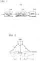
- FIG. 1 is a block diagram showing the structure of a receiving device according to an embodiment B1.
- a receiving device 210 shown in this figure includes a digital signal acquisition circuit 2101, an odd number offset discrete Fourier transform circuit 2102, and a decode circuit 2103.
- the digital signal acquisition circuit 2101 converts received signals (analog signals) into digital signals.
- the odd number offset discrete Fourier transform circuit 2102 applies an offset discrete Fourier transform, which is described later, to digital signals converted according to the received analog signals, and outputs frequency channels corresponding to the received signals.
- the decode circuit 2103 decodes the transmitted signals from the received signals of each of the frequency channels transformed by the odd number offset discrete Fourier transform circuit 2102.
- 'j' represents the imaginary unit. If transformed as in this formula (B1), a received signal can be transformed into a signal in the frequency domain with no discrepancy. However, in the case of transforming into a few frequency channels, since one of the frequency channels corresponds to a DC component, one of the frequency channels cannot be used due to interference power, so that there is a problem in that the throughput drops.
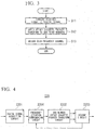
- FIG. 2 is a schematic diagram showing the intensity distribution of a signal at the time of synchronous detection using a reference signal of the central frequency number of a signal.
- reference symbol Q indicates the frequency bands to which three frequency channels of the present embodiment correspond.
- the digital signal acquisition circuit 2101 FIG. 1
- ADC analog to digital converter
- sampling frequency 15 GS/s (giga samples/second)
- FIG. 2 shows the spectrum of a signal in a base band
- a negative frequency less than or equal to the DC component (frequency 0) is defined.
- the ADC operates at 15 GHz
- -7.5 GHz to 0 GHz is equivalent to 7.5 GHz to 15 GHz.
- an offset discrete Fourier transform is applied.
- n complex number sequences Z 0 , ..., Z n-1 can be obtained by the arithmetic expression shown in formula (B2).
- 'j' represents the imaginary unit
- 'n' represents an odd number.
- the number (n) of whole frequency channels acquired by a discrete Fourier transform denotes the "point number" of a discrete Fourier transform.
- the number of frequency channels multiplexed in the frequency domain in the OFDM is an even number (refer to Non-Patent Document 2). It is easier to perform signal processing of data by dealing with every one or an even number of frequency channels. Therefore, in order to acquire signals of an even number of frequency channels using an ADC with a low sampling rate, it is effective to make the point number of the discrete Fourier transform an odd number. In this case, the odd number offset discrete Fourier transform circuit 2102 outputs the results of even numbers of frequency channels at the center, to the decode circuit 2103.
- the phenomenon shown in FIG. 2 in which one of three frequencies extends to a plurality of frequencies also occurs in the case where the point number of the discrete Fourier transform is greater than 3. That is, since the frequency domain signal Z (n-1)/2 corresponding to this frequency band in formula (B2) cannot express a specific frequency, it is incomplete as a transform to the original frequency domain. However, by breaking up such incomplete frequency channel information, the odd number offset discrete Fourier transform circuit 2102 can acquire signals existing in a specific frequency domain.
- the offset discrete Fourier transform in the odd number offset discrete Fourier transform circuit 2102 may be applied to every block, or may be applied as a convolution calculation.
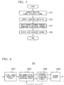
- FIG. 3 is a flow chart showing the processing procedure according to the present embodiment.
- the digital signal acquisition circuit 2101 converts them to digital signals according to the signals received (step S11).
- the odd number offset discrete Fourier transform circuit 2102 applies an offset discrete Fourier transform to the odd point numbers (step S12).
- the decode circuit 2103 decodes the signals of each of the frequency channels corresponding to the acquired signals (step S13).
- the odd number offset discrete Fourier transform circuit 2102 can also compensate for frequency deviation according to the frequency deviation information indicating the frequency deviation of the converted digital signals. Furthermore, the decode circuit 2103 can also feed the estimated frequency deviation signals back to the frequency deviation compensating circuit 2102.
- FIG. 4 is a block diagram showing the structure of a receiving device according to an embodiment B2.
- a receiving device 220 shown in this figure includes a digital signal acquisition circuit 2201, an odd number offset discrete Fourier transform circuit 2202, a decode circuit 2203, and a frequency deviation compensating circuit 2204.
- the digital signal acquisition circuit 2201 converts received signals (analog signals) into digital signals.
- the frequency deviation compensating circuit 2204 compensates for frequency deviation occurring in the received signals using any of the received signals corresponding to the check signals inserted in the transmitted signals, the characteristics of the modulation system of the signals transmitted, and frequency deviation information input from other receiving circuit blocks.
- the frequency deviation occurring in the received signals denotes the frequency deviation between the frequency that generated the transmitted signals and the frequency that the receiving device 220 uses as a reference.
- the odd number offset discrete Fourier transform circuit 2202 applies an offset discrete Fourier transform, which is described later, to digital signals that have been converted according to the received analog signals, and for which the frequency deviation compensating circuit 2204 has compensated for the frequency deviation, and outputs frequency channels corresponding to the received signals.
- the decode circuit 2203 decodes the transmitted signals from the received signals of each of the frequency channels transformed by the odd number offset discrete Fourier transform circuit 2102.
- the frequency deviation compensating circuit 2204 calculates frequency deviation compensated received signals X' k in which the frequency deviation is compensated with respect to the received signals in which frequency deviation occurred using formula (B3).
- X ′ k X k exp ⁇ 2 ⁇ k ⁇ f F s j
- the frequency transform shown in formula (B4) transforms to frequencies which is shifted by half the frequency channel occupying frequency band width.
- the frequency deviation compensating circuit 2204 can also apply a Fourier transform in the odd number offset discrete Fourier transform circuit 2202 after applying the frequency transform shown in formula (B4). In this manner, an offset discrete Fourier transform can also be realized by the frequency deviation compensating circuit 2204 and the odd discrete Fourier transform circuit 2202.
- the frequency deviation signal estimated in the decode circuit 2203 may be fed back as ⁇ f.
- FIG. 5 is a flow chart showing the processing procedure according to the present embodiment.
- the digital signal acquisition circuit 2201 converts them to digital signals according to the signals received (step S21).
- the frequency deviation compensating circuit 2204 compensates for frequency deviation according to frequency deviation information that indicates the frequency deviation of the converted digital signals (step S22).
- the odd number offset discrete Fourier transform circuit 2202 applies an offset discrete Fourier transform to the odd point numbers (step S23).
- the decode circuit 2203 decodes the signals of each of the frequency channels corresponding to the acquired signals (step S24). Furthermore, the decode circuit 2203 feeds the estimated frequency deviation signals back to the frequency deviation compensating circuit 2204 (step S24).
- the frequency deviation information stored in step S24 is derived by calculation processing performed repeatedly, and used as reference information in the frequency deviation compensating circuit 2204.
- FIG. 6 is a block diagram showing the structure of a receiving device according to an embodiment B3.
- a receiving device 230 shown in this figure includes a digital signal acquisition circuit 2301, an odd number offset discrete Fourier transform circuit 2302, a decode circuit 2303, and a frequency deviation estimation circuit 2304.
- the digital signal acquisition circuit 2301 converts received signals (analog signals) into digital signals.
- the frequency deviation estimation circuit 2304 compensates for frequency deviation occurring in the received signals using any of the received signals corresponding to the check signals inserted in the transmitted signals, the characteristics of the modulation system of the transmitted signals, and frequency deviation information input from other receiving circuit blocks.
- the frequency deviation occurring in the received signals denotes the frequency deviation between the frequency that generated the transmitted signals and the frequency that the receiving device 230 uses as a reference.
- the odd number offset discrete Fourier transform circuit 2302 outputs frequency channels corresponding to the received signals, which have been converted according to the received analog signals, and to which an odd number offset discrete Fourier transform is applied in which frequency deviation is considered.
- the frequency deviation estimation circuit 2304 estimates the residual frequency deviation information using digital signals of the frequency channels output from the odd number offset discrete Fourier transform circuit 2302, and outputs them to the odd number offset Fourier transform circuit 2302. Moreover, the frequency deviation estimation circuit 2304 outputs the digital signals to the decode circuit 2303.
- the decode circuit 2303 decodes the transmitted signals from the received signals of each of the frequency channels, which are digital signals output by the frequency deviation estimation circuit 2304, and that are transformed by the odd number offset discrete Fourier transform circuit 2302.
- the signal of the k th frequency channel output is input to the frequency deviation estimation circuit 2304, and the frequency deviation is estimated.
- estimation is possible using for example a frequency deviation compensation method in which a blind algorithm or a known signal proposed for wireless communication is used (for example, refer to Non-Patent Document 4). Since the frequency deviation ⁇ f 0 estimated here is the residual frequency deviation in the offset discrete Fourier transform circuit 2302, the frequency deviation information is updated as ( ⁇ f+ ⁇ f 0 ) in the offset discrete Fourier transform circuit 2302, and thereby it is possible to prevent the interference power due to the frequency deviation from increasing.
- the frequency deviation estimation circuit 2304 can also estimate the frequency deviation with respect to each of the frequency channels, output frequency deviation information to the odd number offset discrete Fourier transform circuit 2302, and compensate for the frequency deviation in each of the frequency channels.
- the decode circuit 2303 can also estimate the frequency deviation in each of the frequency channels, and output it to the odd number offset discrete Fourier transform circuit 2302. In this case, ⁇ f in formula (B5) is different for each of the frequency channels, and ⁇ f k can be used as the frequency deviation of the k th frequency channel.
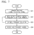
- FIG. 7 is a flow chart showing a processing procedure according to the present embodiment.
- the digital signal acquisition circuit 2301 converts them to digital signals according to the signals received (step S31).
- the odd number offset discrete Fourier transform circuit 2302 compensates for frequency deviation according to frequency deviation information that indicates the frequency deviation of the converted digital signals, and applies an offset discrete Fourier transform to the odd point numbers (step S32).
- the frequency deviation estimation circuit 2304 estimates the residual frequency deviation information using the digital signals of the frequency channels output from the odd number offset discrete Fourier transform circuit 2302, and outputs them to the offset Fourier transform circuit 2302.
- the odd number offset discrete Fourier transform circuit 2302 stores the estimated frequency deviation information in an internal storage section (step S33).
- the frequency deviation estimation circuit 2304 outputs the digital signals to the decode circuit 2303.
- the decode circuit 2303 decodes the signals of each of the frequency channels corresponding to the acquired signals (step S34).
- the frequency deviation information stored in step S34 is derived by calculation processing performed repeatedly by the frequency deviation estimation circuit 2304, and updated.
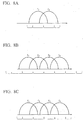
- FIGS. 8A to 8C are diagrams showing the arrangement of frequency channels, and point numbers of an offset discrete Fourier transform.
- FIG. 8A shows an example of a case where the offset discrete Fourier transform circuit 2302 applies a three point offset discrete Fourier transform to two frequency channels as shown in FIG. 2 .
- the offset discrete Fourier transform can be particularly effective.
- FIG. 8B shows a case in which four frequency channels are received, and a seven point offset discrete Fourier transform is performed.
- the sampling frequency of the ADC used to transform the received signals in this case becomes 1.75 times the bandwidth of one frequency channel, and the clock of the ADC can be set 12.5% lower.
- FIG. 8C shows a case in which four frequency channels are received similarly, and a five point offset discrete Fourier transform is performed.
- the sampling frequency of the ADC used to transform the received signals in this case becomes 1.25 times the bandwidth of one frequency channel.
- the clock of the ADC can be set 37.5% lower.
- the oversampling is low, there is a possibility that deterioration of the characteristics occurs.
- k can be from 0 to (n-1).
- it is possible to avoid calculating with respect to Z 1 by applying an offset discrete Fourier transform with n 3, and outputting only Z 0 and Z 2 to the decode circuit.
- the frequency is "0", that is, if it is set such that the DC component is at the boundary of a frequency channel without providing a frequency channel in the DC component, it is possible to reduce the deterioration of the signal quality due to noise and interference corresponding to the DC component.
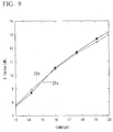
- FIG. 9 is a diagram showing the reception results of a signal that has been polarization multiplexed and transmitted.
- the vertical axis of this figure denotes the Q factor (dB (decibels)), and the horizontal axis denotes the optical signal to noise ratio (OSNR) (dB).
- the reception results shown in the figure are measurements of received signals in communication using a 111 Gb/s (gigabits/second) QPSK (Quadrature Phase Shift Keying) - 2 carrier OFDM (Orthogonal Frequency Division Multiplexing) signal which is polarization multiplexed and transmitted.
- QPSK Quadrature Phase Shift Keying
- OFDM Orthogonal Frequency Division Multiplexing
- the transmitting device transmitted a 111 Gb/s signal as 13.5 Gbaud QPSK signals being two multiplexed in the frequency direction, furthermore being two polarization multiplexed.
- a receiving device In order to receive a two carrier x 13.5 Gbaud signal in a receiving device, it is typically necessary to use a receiving device having an ADC at 55.5 GS/s.(giga samples/second) to extract the corresponding frequency channels and decode it. By contrast, if a receiving device according to the present embodiment is used, it can be decoded using an ADC at 41.6 GS/s.
- FIG. 7 shows the results of resampling and decoding a received signal at 50 GS/s to 55.5 GS/s (graph 2Sb), which are the results of a four point offset discrete Fourier transform.
- graph 2Sa results according to the present embodiment are shown (graph 2Sa) of calculating the Q-factor with respect to the OSNR in the case where a three point offset discrete Fourier transform is applied to a 46.1 GS/s received signal.
- graph 2Sa shows that in the present embodiment (graph 2Sa), although the sampling clock frequency of the ADC is greatly reduced, the results obtained are almost equivalent to the results (graph 2Sb) of a four point offset discrete Fourier transform using 55.5 GS/s data.
- a digital signal acquisition step of the present embodiment acquires digital signals from the received signals that are multiplexed in the frequency domain.
- An offset discrete Fourier transform step applies an offset discrete Fourier transform to odd discrete point numbers based on the acquired digital signals.
- a decode step decodes frequency domain digital signals in the frequency domain obtained by the offset discrete Fourier transform, which are the frequency domain digital signals of one or more frequency channels.
- the odd number offset discrete Fourier transform circuit 2102 select frequency channels corresponding to the transmitted signals appropriately even if the received signals are transformed into signals in the frequency domain using a Fourier transform in the case of receiving a few frequency channels. Furthermore, the digital signal acquisition circuit 2101 enables the sampling frequency of the ADC for acquiring the signal position using a Fourier transform to be reduced.
- the frequency deviation compensation step of the present embodiment compensates for frequency deviation with respect to frequencies of the obtained digital signals.
- the offset discrete Fourier transform step applies an offset discrete Fourier transform to odd discrete point numbers with respect to the digital signals that are frequency transformed to the frequencies in which frequency deviation is been compensated.
- the odd number offset discrete Fourier transform circuit 2102 can apply an offset discrete Fourier transform to the digital signals whose frequency deviation is compensated, it is possible to enhance the accuracy of the offset discrete Fourier transform.
- a frequency deviation estimation step of the present embodiment estimates a residual frequency deviation of each of the frequency channels, or a frequency deviation common to all the frequency channels, from the digital signals transformed into the frequency domain by the offset discrete Fourier transform step, and updates frequency deviation information indicating the frequency deviation.
- the frequency deviation compensation step compensates for frequency deviation with respect to the frequencies of the obtained digital signals based on the frequency deviation information.
- the frequency deviation estimation circuit 2304 can estimate the frequency deviation on the basis of the calculation result, and apply an offset discrete Fourier transform to the digital signals compensated on the basis of the estimated frequency deviation information, it is possible to further enhance the accuracy of the offset discrete Fourier transform.
- the offset discrete Fourier transform step of the present embodiment applies an offset discrete Fourier transform to the odd discrete point numbers using a convolution calculation with respect to digital signals, and calculates and outputs only frequency channels corresponding to the digital signals.
- the odd number offset discrete Fourier transform circuit 2102 can separate the necessary information with no influence from the DC component and the like by performing a convolution calculation on the information of the frequency channels corresponding to the transmitted signals.
- the offset discrete Fourier transform step of the present embodiment acquires, with the discrete point number of the offset discrete Fourier transform being three, two frequency channels out of them.
- the odd number offset discrete Fourier transform circuit 2102 can accumulate unnecessary information such as a DC component in one frequency channel, so that it is possible to increase the quality of the information of the two frequency channels to be acquired.
- the ADC can convert to digital signals using a sampling clock with a frequency of twice the frequency band or less.
- the offset discrete Fourier transform step compensates for an individual frequency deviation in each of the frequency channels.
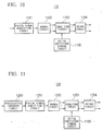
- FIG. 10 is a block diagram showing the structure of a receiving device according to an embodiment A1 of the present invention.
- a receiving device 110 as shown in the figure includes a digital signal acquisition circuit 1101, a branch circuit 1102, an equalizing circuit 1103, a decode circuit 1104, and an initial coefficient storage circuit 1105.
- the digital signal acquisition circuit 1101 converts received analog signals to digital signals.
- the branch circuit 1102 duplicates and branches the digital signals converted by the digital signal acquisition circuit 1101 to channel numbers (L sequences) of the frequency channels for decoding, which are frequency channels contained in the received signals received by the digital signal acquisition circuit 1101.
- the equalizing circuit 1103 equalizes each of the received L sequences signals branched by the branch circuit 1102. For the calculation processing in the equalizing circuit 1103, by utilizing prior knowledge about the desired signals, it is possible to use an equalization algorithm such as a minimum mean squared error (MMSE) method, a maximum SNR (MSN) method, a constrained output power minimization (CMP) method, or a constant modulus signal algorithm (CMA) (refer to Non-Patent Document 4).
- MMSE minimum mean squared error
- MSN maximum SNR
- CMP constrained output power minimization
- CMA constant modulus signal algorithm
- Equalization of the signals of the k th frequency channel can be expressed by the following equation (A1) using an equalization weight w k,i .
- S k,,i denotes a transmitted signal estimated with respect to the i th dispersion time of the k th frequency.
- M denotes the tap number of an equalization weight.
- X i+n-M denotes a received signal at reception timing (i+n-M).
- w k,i denotes the equalization coefficient of an equalization algorithm of the k th subcarrier.
- X x,i+n-M and X Y,i+n-M denote received signals corresponding to the X polarization and Y polarization at the reception timing (i+n-M).
- w XX,k,i denotes an equalization coefficient of an equalization algorithm used for a received X polarization signal in order to acquire a signal of the k th subcarrier transmitted with an X polarization.
- w YX,k,i denotes an equalization coefficient of an equalization algorithm used for a received Y polarization signal in order to obtain a signal of the k th subcarrier transmitted with an X polarization.
- w YY,k,i and w XY,k,i denote an equalization coefficient of an equalization algorithm used for a received X polarization signal and an equalization coefficient of an equalization algorithm used for a received Y polarization signal in order to obtain signals of the k th subcarrier transmitted with a Y polarization.
- the initial coefficient storage circuit 1105 stores coefficients with low correlation as initial weights so that equalization is performed with different weights with respect to each of the signal sequences as initial weights. By setting in this manner, the equalizing circuit can equalize signals corresponding to different frequency bands from each of the branched signal sequences.
- the discrete Fourier transforms can be obtained by the following formula.
- a discrete Fourier transform is applied to n complex series X o, ...,X n-1 , the signal Y k of the k th frequency channel is shown in formula (A3).
- a k,i is an equalization coefficient in a discrete Fourier transform, and this value can be made to be the initial value of the equalization algorithm.
- an initial coefficient can also be made to be the initial coefficient by applying a calculation to the coefficient of the discrete Fourier transform.
- equalization weight w k [w k,1 , w k,2 , ..., w k,M ] T with the tap number being M, which are used for the k th frequency channel, can be applied as [0, 0, ..., 0, a k,0 , a k,1 , ..., a k,n-1 , 0, 0, ...0] T .
- the superscript T is an operator that takes the transpose.
- the equalizing circuit 1103 can equalize the signals of each of the frequency channels.
- the equalizing circuit 1103 it is also possible to apply a constraint condition such that the correlation between w k and w j becomes low under the condition that the converged weight k ⁇ j.
- a relationship that satisfies orthogonal conditions can be applied between the polarizations. For example, in the case where a 2x2 orthogonal Walsh code is used, by setting the initial values of w XX,k and w YX,K to [0, 0, ..., 0, a k,0 , a k,1 , ..., a k,n-1 .
- w XX,k [0, 0, ..., 0, b xx a k, 0, b xx a k,1 , ..., b xx a k,n-1 , 0, 0, ...0] T
- w YX,K [0, 0, ..., 0, b yx a k,0 , b yx a k,1 , ..., b yx a k,n-1 , 0, 0, ...0] T
- w XY,k [0, 0,..., 0, b xy a k,0 , b xy a k,1, .
- b xx , b yx , b xy , b yy , b yy can also be set in each of the frequency channels independently.
- the decode circuit 1104 decodes the signals equalized by the equalizing circuit 1103 according to the encoding system and modulation system.
- the compensation quality of the originally possessed by the equalizer with respect to the time duration of a signal deteriorates with the number of frequency channels n. That is, the receiving device 10 consumes an equivalent quality relative to the time duration of the received signal over the number of frequency channels, n, in the Fourier transform. As a result, the receiving device 110 does not need frequency deviation estimation and compensation in the Fourier transform.
- the frequency can be shifted with respect to each of the frequency channels, and output.
- the k th received signal branched for decoding the k th frequency channel is output from the branch circuit 102 after the following calculation.
- X' k is a signal output from the branch circuit.
- F s is the sampling frequency.
- F k is the central frequency of the k th frequency channel in the receiving device.
- the central frequency of the k th frequency channel used here does not need to be accurate, and it is possible to use an approximate value that is stored in advance or a roughly estimated central position of each of the frequency channels.
- the equalizing circuit can set an equalization weight to the central frequency channel, and can use [0, 0, ... , 0, 1, 1, ...1, 0, 0, ...,0] as initial values of the equalization weights.
- the number of "1's" is n
- the number of "0's" is Nz.
- FIG. 11 is a block diagram showing the structure of a receiving device according to the embodiment A2 of the present invention.
- a receiving device 120 as shown in this figure includes a photoelectric converter circuit 1200, a digital signal acquisition circuit 1201, a branch circuit 1202, an equalizing circuit 1203, a decode circuit 1204, and an initial coefficient storage circuit 1205.
- the receiving device 120 receives optical signals.
- the photoelectric converter circuit 1200 transforms received optical signals into electrical signals.
- the digital signal acquisition circuit 1201 converts the electrical signals transformed by the photoelectric converter circuit 1200 into digital signals.
- the branch circuit 1202 duplicates and branches the digital signals converted by the digital signal acquisition circuit 1201 to channel numbers (L sequences) of the frequency channels for decoding, which are frequency channels contained in the received signals converted by the digital signal acquisition circuit 1201.
- the initial coefficient storage circuit 1205 stores discrete Fourier transform coefficients expressed by formula (A3), or coefficients having high correlation with discrete Fourier transform coefficients, or coefficients that can be expressed using part of them.
- the equalizing circuit 1203 equalizes the L sequences of signals branched by the branch circuit 1202 using the initial weights stored in the initial coefficient storage circuit 1205.
- an equalization algorithm such as a minimum mean squared error (MMSE) method, a maximum SNR (MSN) method, a constrained output power minimization (CMP) method, or a constant modulus signal algorithm (CMA).
- MMSE minimum mean squared error
- MSN maximum SNR
- CMP constrained output power minimization
- CMA constant modulus signal algorithm
- the decode circuit 1204 decodes the signals of specific frequency channels extracted by the equalizing circuit 1203. In optical communication in which synchronous detection is performed, since the wavelength deviation between lasers in a transmitting device and a receiving device is especially great, by not needing a frequency deviation compensation function in a Fourier transform, it is possible to reduce the size of the circuit.
- the branch circuit 1202 can shift the frequencies of signals after branching, and output them similarly to formula (A4).
- the branch circuit 1202 roughly estimates the frequency deviation from known signals contained in the received signals or the spectrum distribution, and shifts the frequency using formula (A4) in respect of all the sequences, so that it is possible to improve the transmission quality of the signals after branching.
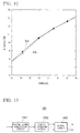
- FIG. 12 is a diagram showing reception results of a signal that has been polarization multiplexed and transmitted.
- the vertical axis of this figure denotes the Q factor (dB), and the horizontal axis denotes the optical signal to noise ratio (OSNR) (dB).
- Q factor the Q factor
- OSNR optical signal to noise ratio
- the reception results shown in this figure are measurements of received signals in communication using a 111 Gb/s (gigabits/second) QPSK (Quadrature Phase Shift Keying) - 2 carrier OFDM (Orthogonal Frequency Division Multiplexing) signal which is polarization multiplexed and transmitted.
- QPSK Quadrature Phase Shift Keying
- OFDM Orthogonal Frequency Division Multiplexing
- FIG. 12 shows that the same characteristics were obtained in the case where a Fourier transform was applied (graph 1Sb) and the case where equalization was performed without it (graph 1Sa). As shown in FIG. 12 , it can be confirmed that in the present embodiment, although a Fourier transform and frequency deviation estimation have not been performed prior, the same characteristics are obtained as in the results of decoding after a discrete Fourier transform has been applied.
- CMA constant modulus algorithm
- the greater the frequency deviation the greater the effect.
- the receiving device shown in the present embodiment by providing a channel that is used for a Fourier transform, there is a case in which a drop occurs in the tolerance against polarization mode dispersion.
- the digital signal acquisition circuit 1101 acquires digital signals from the received signals that are multiplexed in the frequency domain.
- the branch circuit 1102 branches the obtained digital signals to frequency channel numbers for decoding.
- the initial coefficient storage circuit 1105 stores coefficients with low and different correlation with respect to each of the signal sequences as initial weights.
- the equalizing circuit 1103 equalizes the branched signal sequences using the different coefficients.
- the decode circuit 1104 decodes each of the equalized signal sequences.
- the digital signal acquisition circuit 1101 acquires digital signals from received signals that are multiplexed in the frequency domain.
- the branch circuit 1102 branches the obtained digital signals to frequency channel numbers for decoding.
- the initial coefficient storage circuit 1105 stores coefficients having high correlation with the coefficients of the discrete Fourier transform corresponding to each of the frequency channels, or coefficients including at least part of them, as initial weights with respect to each of the branched signal sequences.
- the equalizing circuit 1103 equalizes the coefficients stored in the initial coefficient storage step as initial weights.
- the decode circuit 1104 decodes each of the equalized signal sequences.
- the equalizing circuit 1103 blindly equalizing the coefficients of a discrete Fourier transform for acquiring the central frequency of each of the frequency channels as initial values, it is possible to decode the signals transmitted by the orthogonal frequency division multiplexing system without applying discrete Fourier transforms to the frequency channels for equalizing.
- the initial coefficient storage circuit 1105 stores coefficients having high correlation with the coefficients of the discrete Fourier transform corresponding to the specific frequency component, or coefficients including at least part of them, as initial weights.
- the equalization coefficients are adjusted such that none of the signal sequences equalized in the equalizing circuit 1103 converges to a signal sequences indicating the same signal.
- the equalized signals are prevented from being the same signal, so that it is possible to decode the signals transmitted by the orthogonal frequency division multiplexing system without applying a discrete Fourier transform.
- the present invention can be used for a method for receiving frequency domain multiplexed signals and a device for receiving frequency domain multiplexed signals. According to the method for receiving frequency domain multiplexed signals and the device for receiving frequency domain multiplexed signals, sampling is possible with a lower frequency than that of twice the frequency band of the received signals.
Claims (5)
- Empfangsverfahren für ein Frequenzdomain-multiplexiertes Signal, welches empfangene Signale decodiert, die in einer Frequenzdomain multiplexiert sind, wobei das Verfahren umfasst:einen Digitalsignal-Erfassungsschritt zum Erfassen von Digitalsignalen aus den empfangenen Signalen, die in der Frequenzdomain multiplexiert sind;einen Verzweigungsschritt zum Verzweigen der erhaltenen Digitalsignale, um Frequenzkanalnummern von verzweigten Signalsequenzen zum Decodieren zu erhalten;einen Entzerrungsschritt zum Entzerren jeder der verzweigten Signalsequenzen; undeinen Decodierschritt zum Decodieren jeder der verzweigten Signalsequenzen,dadurch gekennzeichnet ist, dass es ferner umfasst:einen Initialer-Koeffizient-Speicherungsschritt zum Speichern, unter Verwendung von Koeffizienten ak,0, ak,1, ..., ak,n-1 einer n-Punkt-diskreten FourierTransformation, von Koeffizienten [0, 0, ..., 0, ak,0, ak,1, ..., ak,n-1,0, 0, ...,0]T als initialen Gewichten von Entzerrungsgewichten wk = [wk,1, wk,2, ..., wk,M]T mit einer Abtastzahl, die M ist, welche für einen k-ten Frequenzkanal unter den verzweigten Signalsequenzen verwendet werden,wobei der Entzerrungsschritt die dem k-ten Frequenzkanal entsprechende verzweigte Signalsequenz unter Verwendung der in dem Initialer-Koeffizient-Speicherungsschritt gespeicherten Koeffizienten als den initialen Gewichten entzerrt, unter Verwendung einer Formel:

- Empfangsverfahren für ein Frequenzdomain-multiplexiertes Signal nach Anspruch 1,
wobei der Verzweigungsschritt verzweigt, wenn die Digitalsignale verzweigt werden, nach Anwenden einer Frequenztransformation, sodass eine Zentralfrequenz jedes der Frequenzkanäle sich der Umgebung einer spezifischen Frequenzkomponente annähert. - Empfangsverfahren für ein Frequenzdomain-multiplexiertes Signal nach einem der Ansprüche 1 oder 2, wobei Entzerrungskoeffizienten so angepasst sind, dass jede der in dem Entzerrungsschritt entzerrten Signalsequenzen nicht zu Signalsequenzen konvergiert, die dasselbe Signal angeben.
- Empfangsgerät (110, 120) für ein Frequenzdomain-multiplexiertes Signal, das so konfiguriert ist, dass es empfangene Signale decodiert, die multiplexiert in einer Frequenzdomain sind, das Gerät umfassend:einen Digitalsignal-Erfassungsabschnitt (1101, 1201), der so konfiguriert ist, dass er Digitalsignale aus empfangenen Signalen erfasst, die multiplexiert in der Frequenzdomain sind;einen Verzweigungsabschnitt (1102, 1202), der so konfiguriert ist, dass er die erhaltenen Digitalsignale verzweigt, um die Frequenzkanalnummern von verzweigten Signalsequenzen für das Decodieren zu erhalten;einen Entzerrungsabschnitt (1103, 1203), der so konfiguriert ist, dass er jede der verzweigten Signalsequenzen entzerrt; undeinen Decodierabschnitt (1104, 1204), der so konfiguriert ist, dass er jede der entzerrten Signalsequenzen decodiert, dadurch gekennzeichnet, dass es ferner umfasst:einen Initialer-Koeffizient-Speicherabschnitt (1105, 1205), der so konfiguriert ist, dass er, unter Verwendung von Koeffizienten ak,0, ak,1, ..., ak,n-1 einer n-Punkt-diskreten Fourier-Transformation, als initiale Gewichte von Entzerrungsgewichten wk = [wk,1, wk,2, wk,M]T mit einer Abtastzahl, die M ist, Koeffizienten [0, 0, ..., 0, ak,0, ak,1, ..., ak,n-1,0, 0, ...,0]T speichert, welche für einen k-ten Frequenzkanal unter den verzweigten Signalsequenzen verwendet werden,wobei der Entzerrungsabschnitt so konfiguriert ist, dass er die dem k-ten Frequenzkanal entsprechende verzweigte Signalsequenz, unter Verwendung der in dem Initialer-Koeffizient-Speicherungsabschnitt gespeicherten Koeffizienten als den initialen Gewichten, entzerrt, unter Verwendung einer Formel:

- Empfangsgerät für ein Frequenzdomain-multiplexiertes Signal (120) nach Anspruch 4, wobei:die empfangenen Signale optische Signale sind;das Empfangsgerät für ein Frequenzdomain-multiplexiertes Signal ferner einen photoelektrischen Wandlerabschnitt (1200) umfasst, der so konfiguriert ist, dass er die optischen Signale in elektrische Signale umwandelt; unddie Digitalsignale in dem Digitalsignal-Erfassungsabschnitt aus den elektrischen Signalen erfasst sind.
Applications Claiming Priority (3)
| Application Number | Priority Date | Filing Date | Title |
|---|---|---|---|
| JP2009169460 | 2009-07-17 | ||
| JP2009169455 | 2009-07-17 | ||
| EP10799887.4A EP2456107B1 (de) | 2009-07-17 | 2010-07-15 | Verfahren zum Empfangen eines Frequenzdomänen-Multiplexsignals und Vorrichtung zum Empfangen eines Frequenzdomänen-Multiplexsignals |
Related Parent Applications (3)
| Application Number | Title | Priority Date | Filing Date |
|---|---|---|---|
| EP10799887.4A Division EP2456107B1 (de) | 2009-07-17 | 2010-07-15 | Verfahren zum Empfangen eines Frequenzdomänen-Multiplexsignals und Vorrichtung zum Empfangen eines Frequenzdomänen-Multiplexsignals |
| EP10799887.4A Division-Into EP2456107B1 (de) | 2009-07-17 | 2010-07-15 | Verfahren zum Empfangen eines Frequenzdomänen-Multiplexsignals und Vorrichtung zum Empfangen eines Frequenzdomänen-Multiplexsignals |
| EP10799887.4 Division | 2010-07-15 |
Publications (2)
| Publication Number | Publication Date |
|---|---|
| EP2658198A1 EP2658198A1 (de) | 2013-10-30 |
| EP2658198B1 true EP2658198B1 (de) | 2016-10-19 |
Family
ID=43449438
Family Applications (2)
| Application Number | Title | Priority Date | Filing Date |
|---|---|---|---|
| EP13177394.7A Active EP2658198B1 (de) | 2009-07-17 | 2010-07-15 | Verfahren zum empfangen eines frequenzdomänen-multiplexsignals und vorrichtung zum empfangen eines frequenzdomänen-multiplexsignals |
| EP10799887.4A Active EP2456107B1 (de) | 2009-07-17 | 2010-07-15 | Verfahren zum Empfangen eines Frequenzdomänen-Multiplexsignals und Vorrichtung zum Empfangen eines Frequenzdomänen-Multiplexsignals |
Family Applications After (1)
| Application Number | Title | Priority Date | Filing Date |
|---|---|---|---|
| EP10799887.4A Active EP2456107B1 (de) | 2009-07-17 | 2010-07-15 | Verfahren zum Empfangen eines Frequenzdomänen-Multiplexsignals und Vorrichtung zum Empfangen eines Frequenzdomänen-Multiplexsignals |
Country Status (5)
| Country | Link |
|---|---|
| US (1) | US9160600B2 (de) |
| EP (2) | EP2658198B1 (de) |
| JP (2) | JP5318207B2 (de) |
| CN (1) | CN102484549B (de) |
| WO (1) | WO2011007829A1 (de) |
Families Citing this family (7)
| Publication number | Priority date | Publication date | Assignee | Title |
|---|---|---|---|---|
| US9048953B2 (en) * | 2010-11-29 | 2015-06-02 | Hitachi, Ltd. | Optical communication system, optical transmitter, and transponder |
| CN103916148B (zh) * | 2013-01-05 | 2016-08-03 | 华为技术有限公司 | 一种自适应射频干扰抵消装置、方法、接收机及通信系统 |
| EP3032790B1 (de) * | 2014-12-08 | 2018-02-21 | Vodafone GmbH | Verallgemeinerte frequenzmultiplexierungs-funkübertragung mithilfe frequenzbereich-offset-qam |
| US9973364B2 (en) * | 2016-06-27 | 2018-05-15 | Intel IP Corporation | Generalized frequency division multiplexing (GFDM) frame strucutre for IEEE 802.11AY |
| CN108226598B (zh) * | 2018-01-05 | 2020-11-10 | 深圳市道通科技股份有限公司 | 一种示波器信号译码方法、装置及示波器 |
| CN111698026B (zh) * | 2019-03-12 | 2023-05-12 | 富士通株式会社 | 偏振态变化监测方法、装置和接收机 |
| CN112101179A (zh) * | 2020-09-10 | 2020-12-18 | 国网江苏省电力有限公司信息通信分公司 | 一种抗信道干扰瞬态射频指纹特征提取方法 |
Family Cites Families (18)
| Publication number | Priority date | Publication date | Assignee | Title |
|---|---|---|---|---|
| US4300229A (en) | 1979-02-21 | 1981-11-10 | Nippon Electric Co., Ltd. | Transmitter and receiver for an othogonally multiplexed QAM signal of a sampling rate N times that of PAM signals, comprising an N/2-point offset fourier transform processor |
| JPH0746224A (ja) * | 1992-10-09 | 1995-02-14 | Philips Electron Nv | 送信システム及び受信機 |
| US7440498B2 (en) * | 2002-12-17 | 2008-10-21 | Tellabs Operations, Inc. | Time domain equalization for discrete multi-tone systems |
| US6631175B2 (en) | 1998-04-03 | 2003-10-07 | Tellabs Operations, Inc. | Spectrally constrained impulse shortening filter for a discrete multi-tone receiver |
| EP1063824B1 (de) * | 1999-06-22 | 2006-08-02 | Matsushita Electric Industrial Co., Ltd. | Symboltaktsynchronisierung in Mehrträgerempfängern |
| US6532258B1 (en) * | 1999-06-24 | 2003-03-11 | Ibiquity Digital Corporation | Method for estimating signal-to-noise ratio of digital carriers in an AM compatible digital audio broadcasting system |
| US6771591B1 (en) * | 2000-07-31 | 2004-08-03 | Thomson Licensing S.A. | Method and system for processing orthogonal frequency division multiplexed signals |
| JP4465931B2 (ja) * | 2001-07-19 | 2010-05-26 | 株式会社富士通ゼネラル | Ofdm復調器用等化器 |
| US7352806B2 (en) * | 2001-12-06 | 2008-04-01 | Tensorcom, Inc. | Systems and methods for transmitting data in a wireless communication network |
| US7317750B2 (en) | 2002-10-31 | 2008-01-08 | Lot 41 Acquisition Foundation, Llc | Orthogonal superposition coding for direct-sequence communications |
| KR100463544B1 (ko) * | 2002-12-14 | 2004-12-29 | 엘지전자 주식회사 | 채널 등화 장치 및 이를 이용한 디지털 tv 수신기 |
| US7580454B2 (en) * | 2004-07-14 | 2009-08-25 | Fundacion Tarpuy | Multidimensional decision-directed trained adaptive equalization |
| US8665799B2 (en) * | 2006-09-14 | 2014-03-04 | Qualcomm Incorporated | Beacon assisted cell search in a wireless communication system |
| US20080273480A1 (en) * | 2007-05-02 | 2008-11-06 | Mediaphy Corporation | Dynamic adjustment of training time for wireless receiver |
| JP2009141514A (ja) * | 2007-12-04 | 2009-06-25 | Nippon Telegr & Teleph Corp <Ntt> | チャネル推定装置及び無線通信システム |
| JP5347271B2 (ja) | 2008-01-10 | 2013-11-20 | カシオ計算機株式会社 | 端末装置及びプログラム |
| JP2009169460A (ja) | 2008-01-10 | 2009-07-30 | Sharp Corp | コンテンツ自動コピーシステム |
| US8125885B2 (en) * | 2008-07-11 | 2012-02-28 | Texas Instruments Incorporated | Frequency offset estimation in orthogonal frequency division multiple access wireless networks |
-
2010
- 2010-07-15 CN CN201080028997.1A patent/CN102484549B/zh active Active
- 2010-07-15 EP EP13177394.7A patent/EP2658198B1/de active Active
- 2010-07-15 EP EP10799887.4A patent/EP2456107B1/de active Active
- 2010-07-15 JP JP2011522847A patent/JP5318207B2/ja active Active
- 2010-07-15 US US13/381,114 patent/US9160600B2/en active Active
- 2010-07-15 WO PCT/JP2010/061972 patent/WO2011007829A1/ja active Application Filing
-
2013
- 2013-06-14 JP JP2013126142A patent/JP5576533B2/ja active Active
Also Published As
| Publication number | Publication date |
|---|---|
| CN102484549B (zh) | 2015-02-18 |
| US9160600B2 (en) | 2015-10-13 |
| EP2456107A4 (de) | 2013-02-20 |
| CN102484549A (zh) | 2012-05-30 |
| US20120106618A1 (en) | 2012-05-03 |
| EP2456107A1 (de) | 2012-05-23 |
| JPWO2011007829A1 (ja) | 2012-12-27 |
| JP2013179705A (ja) | 2013-09-09 |
| WO2011007829A1 (ja) | 2011-01-20 |
| JP5318207B2 (ja) | 2013-10-16 |
| EP2658198A1 (de) | 2013-10-30 |
| JP5576533B2 (ja) | 2014-08-20 |
| EP2456107B1 (de) | 2014-02-26 |
Similar Documents
| Publication | Publication Date | Title |
|---|---|---|
| EP2658198B1 (de) | Verfahren zum empfangen eines frequenzdomänen-multiplexsignals und vorrichtung zum empfangen eines frequenzdomänen-multiplexsignals | |
| EP2434665B1 (de) | Signalerzeugungsschaltung, überträger für optische signale, signalempfangsschaltung, verfahren zur synchronisation optischer signale und system zur synchronisation optischer signale | |
| US8787769B2 (en) | Chromatic dispersion value calculating apparatus, optical signal receiving apparatus, optical signal transmitting apparatus, and chromatic dispersion value calculation method | |
| US8279953B2 (en) | Transmitting apparatus, receiving apparatus, and wireless communication method | |
| US20180076916A1 (en) | System and method for ofdm symbol interleaving | |
| EP2247012A1 (de) | Optischer ofdm-empfänger, optisches übertragungssystem, unterträger-trennschaltung und unterträger-trennverfahren | |
| EP3926860B1 (de) | Trainingsgestützte vorwärtsgerichtete kanalentzerrung | |
| WO2012049912A1 (ja) | 送信装置、受信装置および中継装置 | |
| EP2355432A1 (de) | Verfahren und Anordnung zur Übertragung eines orthogonalen Frequenzdiversitätsmultiplexsignals über mindestens einen optischen Filter | |
| JP2023063488A (ja) | ディジタル信号処理装置 | |
| WO2013139395A1 (en) | Method for digitally compensating a phase response of an optical channel | |
| EP2568636B1 (de) | Optisches PDM-QAM-Burst-Mode-System mit OFDM-Synchronisationssymbolen | |
| US10505641B2 (en) | Clock recovery for band-limited optical channels | |
| US11632184B2 (en) | Wavelength-division multiplexing optical transmission system, wavelength-division multiplexing optical transmission method, and non-transitory computer readable medium | |
| JP5796888B2 (ja) | 光直交周波数分割多重伝送方式による受信装置および受信方法 | |
| EP3133751A1 (de) | Verfahren zur nichtlinearitätskompensierung in optischen übertragungssystemen | |
| KR20080068412A (ko) | 통신 시스템에서 신호 송수신 장치 및 방법 | |
| GB2478604A (en) | Wireless communications channel estimation |
Legal Events
| Date | Code | Title | Description |
|---|---|---|---|
| PUAI | Public reference made under article 153(3) epc to a published international application that has entered the european phase |
Free format text: ORIGINAL CODE: 0009012 |
|
| 17P | Request for examination filed |
Effective date: 20130722 |
|
| AC | Divisional application: reference to earlier application |
Ref document number: 2456107 Country of ref document: EP Kind code of ref document: P |
|
| AK | Designated contracting states |
Kind code of ref document: A1 Designated state(s): AL AT BE BG CH CY CZ DE DK EE ES FI FR GB GR HR HU IE IS IT LI LT LU LV MC MK MT NL NO PL PT RO SE SI SK SM TR |
|
| RBV | Designated contracting states (corrected) |
Designated state(s): AL AT BE BG CH CY CZ DE DK EE ES FI FR GB GR HR HU IE IS IT LI LT LU LV MC MK MT NL NO PL PT RO SE SI SK SM TR |
|
| 17Q | First examination report despatched |
Effective date: 20150424 |
|
| GRAP | Despatch of communication of intention to grant a patent |
Free format text: ORIGINAL CODE: EPIDOSNIGR1 |
|
| INTG | Intention to grant announced |
Effective date: 20160527 |
|
| GRAS | Grant fee paid |
Free format text: ORIGINAL CODE: EPIDOSNIGR3 |
|
| GRAA | (expected) grant |
Free format text: ORIGINAL CODE: 0009210 |
|
| AC | Divisional application: reference to earlier application |
Ref document number: 2456107 Country of ref document: EP Kind code of ref document: P |
|
| AK | Designated contracting states |
Kind code of ref document: B1 Designated state(s): AL AT BE BG CH CY CZ DE DK EE ES FI FR GB GR HR HU IE IS IT LI LT LU LV MC MK MT NL NO PL PT RO SE SI SK SM TR |
|
| REG | Reference to a national code |
Ref country code: GB Ref legal event code: FG4D |
|
| REG | Reference to a national code |
Ref country code: CH Ref legal event code: EP |
|
| REG | Reference to a national code |
Ref country code: AT Ref legal event code: REF Ref document number: 839147 Country of ref document: AT Kind code of ref document: T Effective date: 20161115 |
|
| REG | Reference to a national code |
Ref country code: IE Ref legal event code: FG4D |
|
| REG | Reference to a national code |
Ref country code: DE Ref legal event code: R096 Ref document number: 602010037406 Country of ref document: DE |
|
| REG | Reference to a national code |
Ref country code: NL Ref legal event code: MP Effective date: 20161019 |
|
| REG | Reference to a national code |
Ref country code: LT Ref legal event code: MG4D |
|
| PG25 | Lapsed in a contracting state [announced via postgrant information from national office to epo] |
Ref country code: LV Free format text: LAPSE BECAUSE OF FAILURE TO SUBMIT A TRANSLATION OF THE DESCRIPTION OR TO PAY THE FEE WITHIN THE PRESCRIBED TIME-LIMIT Effective date: 20161019 |
|
| REG | Reference to a national code |
Ref country code: AT Ref legal event code: MK05 Ref document number: 839147 Country of ref document: AT Kind code of ref document: T Effective date: 20161019 |
|
| PG25 | Lapsed in a contracting state [announced via postgrant information from national office to epo] |
Ref country code: SE Free format text: LAPSE BECAUSE OF FAILURE TO SUBMIT A TRANSLATION OF THE DESCRIPTION OR TO PAY THE FEE WITHIN THE PRESCRIBED TIME-LIMIT Effective date: 20161019 Ref country code: NO Free format text: LAPSE BECAUSE OF FAILURE TO SUBMIT A TRANSLATION OF THE DESCRIPTION OR TO PAY THE FEE WITHIN THE PRESCRIBED TIME-LIMIT Effective date: 20170119 Ref country code: GR Free format text: LAPSE BECAUSE OF FAILURE TO SUBMIT A TRANSLATION OF THE DESCRIPTION OR TO PAY THE FEE WITHIN THE PRESCRIBED TIME-LIMIT Effective date: 20170120 Ref country code: LT Free format text: LAPSE BECAUSE OF FAILURE TO SUBMIT A TRANSLATION OF THE DESCRIPTION OR TO PAY THE FEE WITHIN THE PRESCRIBED TIME-LIMIT Effective date: 20161019 |
|
| PG25 | Lapsed in a contracting state [announced via postgrant information from national office to epo] |
Ref country code: ES Free format text: LAPSE BECAUSE OF FAILURE TO SUBMIT A TRANSLATION OF THE DESCRIPTION OR TO PAY THE FEE WITHIN THE PRESCRIBED TIME-LIMIT Effective date: 20161019 Ref country code: PL Free format text: LAPSE BECAUSE OF FAILURE TO SUBMIT A TRANSLATION OF THE DESCRIPTION OR TO PAY THE FEE WITHIN THE PRESCRIBED TIME-LIMIT Effective date: 20161019 Ref country code: HR Free format text: LAPSE BECAUSE OF FAILURE TO SUBMIT A TRANSLATION OF THE DESCRIPTION OR TO PAY THE FEE WITHIN THE PRESCRIBED TIME-LIMIT Effective date: 20161019 Ref country code: BE Free format text: LAPSE BECAUSE OF FAILURE TO SUBMIT A TRANSLATION OF THE DESCRIPTION OR TO PAY THE FEE WITHIN THE PRESCRIBED TIME-LIMIT Effective date: 20161019 Ref country code: PT Free format text: LAPSE BECAUSE OF FAILURE TO SUBMIT A TRANSLATION OF THE DESCRIPTION OR TO PAY THE FEE WITHIN THE PRESCRIBED TIME-LIMIT Effective date: 20170220 Ref country code: NL Free format text: LAPSE BECAUSE OF FAILURE TO SUBMIT A TRANSLATION OF THE DESCRIPTION OR TO PAY THE FEE WITHIN THE PRESCRIBED TIME-LIMIT Effective date: 20161019 Ref country code: FI Free format text: LAPSE BECAUSE OF FAILURE TO SUBMIT A TRANSLATION OF THE DESCRIPTION OR TO PAY THE FEE WITHIN THE PRESCRIBED TIME-LIMIT Effective date: 20161019 Ref country code: AT Free format text: LAPSE BECAUSE OF FAILURE TO SUBMIT A TRANSLATION OF THE DESCRIPTION OR TO PAY THE FEE WITHIN THE PRESCRIBED TIME-LIMIT Effective date: 20161019 Ref country code: IS Free format text: LAPSE BECAUSE OF FAILURE TO SUBMIT A TRANSLATION OF THE DESCRIPTION OR TO PAY THE FEE WITHIN THE PRESCRIBED TIME-LIMIT Effective date: 20170219 |
|
| REG | Reference to a national code |
Ref country code: DE Ref legal event code: R097 Ref document number: 602010037406 Country of ref document: DE |
|
| REG | Reference to a national code |
Ref country code: FR Ref legal event code: PLFP Year of fee payment: 8 |
|
| PG25 | Lapsed in a contracting state [announced via postgrant information from national office to epo] |
Ref country code: DK Free format text: LAPSE BECAUSE OF FAILURE TO SUBMIT A TRANSLATION OF THE DESCRIPTION OR TO PAY THE FEE WITHIN THE PRESCRIBED TIME-LIMIT Effective date: 20161019 Ref country code: CZ Free format text: LAPSE BECAUSE OF FAILURE TO SUBMIT A TRANSLATION OF THE DESCRIPTION OR TO PAY THE FEE WITHIN THE PRESCRIBED TIME-LIMIT Effective date: 20161019 Ref country code: EE Free format text: LAPSE BECAUSE OF FAILURE TO SUBMIT A TRANSLATION OF THE DESCRIPTION OR TO PAY THE FEE WITHIN THE PRESCRIBED TIME-LIMIT Effective date: 20161019 Ref country code: SK Free format text: LAPSE BECAUSE OF FAILURE TO SUBMIT A TRANSLATION OF THE DESCRIPTION OR TO PAY THE FEE WITHIN THE PRESCRIBED TIME-LIMIT Effective date: 20161019 Ref country code: RO Free format text: LAPSE BECAUSE OF FAILURE TO SUBMIT A TRANSLATION OF THE DESCRIPTION OR TO PAY THE FEE WITHIN THE PRESCRIBED TIME-LIMIT Effective date: 20161019 |
|
| PLBE | No opposition filed within time limit |
Free format text: ORIGINAL CODE: 0009261 |
|
| STAA | Information on the status of an ep patent application or granted ep patent |
Free format text: STATUS: NO OPPOSITION FILED WITHIN TIME LIMIT |
|
| PG25 | Lapsed in a contracting state [announced via postgrant information from national office to epo] |
Ref country code: SM Free format text: LAPSE BECAUSE OF FAILURE TO SUBMIT A TRANSLATION OF THE DESCRIPTION OR TO PAY THE FEE WITHIN THE PRESCRIBED TIME-LIMIT Effective date: 20161019 Ref country code: BG Free format text: LAPSE BECAUSE OF FAILURE TO SUBMIT A TRANSLATION OF THE DESCRIPTION OR TO PAY THE FEE WITHIN THE PRESCRIBED TIME-LIMIT Effective date: 20170119 Ref country code: IT Free format text: LAPSE BECAUSE OF FAILURE TO SUBMIT A TRANSLATION OF THE DESCRIPTION OR TO PAY THE FEE WITHIN THE PRESCRIBED TIME-LIMIT Effective date: 20161019 |
|
| 26N | No opposition filed |
Effective date: 20170720 |
|
| PG25 | Lapsed in a contracting state [announced via postgrant information from national office to epo] |
Ref country code: SI Free format text: LAPSE BECAUSE OF FAILURE TO SUBMIT A TRANSLATION OF THE DESCRIPTION OR TO PAY THE FEE WITHIN THE PRESCRIBED TIME-LIMIT Effective date: 20161019 |
|
| REG | Reference to a national code |
Ref country code: CH Ref legal event code: PL |
|
| REG | Reference to a national code |
Ref country code: IE Ref legal event code: MM4A |
|
| PG25 | Lapsed in a contracting state [announced via postgrant information from national office to epo] |
Ref country code: IE Free format text: LAPSE BECAUSE OF NON-PAYMENT OF DUE FEES Effective date: 20170715 Ref country code: LI Free format text: LAPSE BECAUSE OF NON-PAYMENT OF DUE FEES Effective date: 20170731 Ref country code: CH Free format text: LAPSE BECAUSE OF NON-PAYMENT OF DUE FEES Effective date: 20170731 |
|
| PG25 | Lapsed in a contracting state [announced via postgrant information from national office to epo] |
Ref country code: LU Free format text: LAPSE BECAUSE OF NON-PAYMENT OF DUE FEES Effective date: 20170715 |
|
| REG | Reference to a national code |
Ref country code: FR Ref legal event code: PLFP Year of fee payment: 9 |
|
| PG25 | Lapsed in a contracting state [announced via postgrant information from national office to epo] |
Ref country code: MT Free format text: LAPSE BECAUSE OF NON-PAYMENT OF DUE FEES Effective date: 20170715 |
|
| PG25 | Lapsed in a contracting state [announced via postgrant information from national office to epo] |
Ref country code: MC Free format text: LAPSE BECAUSE OF FAILURE TO SUBMIT A TRANSLATION OF THE DESCRIPTION OR TO PAY THE FEE WITHIN THE PRESCRIBED TIME-LIMIT Effective date: 20161019 Ref country code: HU Free format text: LAPSE BECAUSE OF FAILURE TO SUBMIT A TRANSLATION OF THE DESCRIPTION OR TO PAY THE FEE WITHIN THE PRESCRIBED TIME-LIMIT; INVALID AB INITIO Effective date: 20100715 |
|
| PG25 | Lapsed in a contracting state [announced via postgrant information from national office to epo] |
Ref country code: CY Free format text: LAPSE BECAUSE OF NON-PAYMENT OF DUE FEES Effective date: 20161019 |
|
| PG25 | Lapsed in a contracting state [announced via postgrant information from national office to epo] |
Ref country code: MK Free format text: LAPSE BECAUSE OF FAILURE TO SUBMIT A TRANSLATION OF THE DESCRIPTION OR TO PAY THE FEE WITHIN THE PRESCRIBED TIME-LIMIT Effective date: 20161019 |
|
| PG25 | Lapsed in a contracting state [announced via postgrant information from national office to epo] |
Ref country code: TR Free format text: LAPSE BECAUSE OF FAILURE TO SUBMIT A TRANSLATION OF THE DESCRIPTION OR TO PAY THE FEE WITHIN THE PRESCRIBED TIME-LIMIT Effective date: 20161019 |
|
| PG25 | Lapsed in a contracting state [announced via postgrant information from national office to epo] |
Ref country code: AL Free format text: LAPSE BECAUSE OF FAILURE TO SUBMIT A TRANSLATION OF THE DESCRIPTION OR TO PAY THE FEE WITHIN THE PRESCRIBED TIME-LIMIT Effective date: 20161019 |
|
| PGFP | Annual fee paid to national office [announced via postgrant information from national office to epo] |
Ref country code: GB Payment date: 20230720 Year of fee payment: 14 |
|
| PGFP | Annual fee paid to national office [announced via postgrant information from national office to epo] |
Ref country code: FR Payment date: 20230725 Year of fee payment: 14 Ref country code: DE Payment date: 20230719 Year of fee payment: 14 |