EP2657752A2 - Display device - Google Patents
Display device Download PDFInfo
- Publication number
- EP2657752A2 EP2657752A2 EP12007996.7A EP12007996A EP2657752A2 EP 2657752 A2 EP2657752 A2 EP 2657752A2 EP 12007996 A EP12007996 A EP 12007996A EP 2657752 A2 EP2657752 A2 EP 2657752A2
- Authority
- EP
- European Patent Office
- Prior art keywords
- display panel
- display device
- display
- main frame
- top case
- Prior art date
- Legal status (The legal status is an assumption and is not a legal conclusion. Google has not performed a legal analysis and makes no representation as to the accuracy of the status listed.)
- Granted
Links
Images




Classifications
-
- G—PHYSICS
- G09—EDUCATION; CRYPTOGRAPHY; DISPLAY; ADVERTISING; SEALS
- G09F—DISPLAYING; ADVERTISING; SIGNS; LABELS OR NAME-PLATES; SEALS
- G09F9/00—Indicating arrangements for variable information in which the information is built-up on a support by selection or combination of individual elements
- G09F9/30—Indicating arrangements for variable information in which the information is built-up on a support by selection or combination of individual elements in which the desired character or characters are formed by combining individual elements
- G09F9/35—Indicating arrangements for variable information in which the information is built-up on a support by selection or combination of individual elements in which the desired character or characters are formed by combining individual elements being liquid crystals
-
- G—PHYSICS
- G02—OPTICS
- G02F—OPTICAL DEVICES OR ARRANGEMENTS FOR THE CONTROL OF LIGHT BY MODIFICATION OF THE OPTICAL PROPERTIES OF THE MEDIA OF THE ELEMENTS INVOLVED THEREIN; NON-LINEAR OPTICS; FREQUENCY-CHANGING OF LIGHT; OPTICAL LOGIC ELEMENTS; OPTICAL ANALOGUE/DIGITAL CONVERTERS
- G02F1/00—Devices or arrangements for the control of the intensity, colour, phase, polarisation or direction of light arriving from an independent light source, e.g. switching, gating or modulating; Non-linear optics
- G02F1/01—Devices or arrangements for the control of the intensity, colour, phase, polarisation or direction of light arriving from an independent light source, e.g. switching, gating or modulating; Non-linear optics for the control of the intensity, phase, polarisation or colour
- G02F1/13—Devices or arrangements for the control of the intensity, colour, phase, polarisation or direction of light arriving from an independent light source, e.g. switching, gating or modulating; Non-linear optics for the control of the intensity, phase, polarisation or colour based on liquid crystals, e.g. single liquid crystal display cells
- G02F1/133—Constructional arrangements; Operation of liquid crystal cells; Circuit arrangements
- G02F1/1333—Constructional arrangements; Manufacturing methods
- G02F1/133308—Support structures for LCD panels, e.g. frames or bezels
-
- G—PHYSICS
- G02—OPTICS
- G02F—OPTICAL DEVICES OR ARRANGEMENTS FOR THE CONTROL OF LIGHT BY MODIFICATION OF THE OPTICAL PROPERTIES OF THE MEDIA OF THE ELEMENTS INVOLVED THEREIN; NON-LINEAR OPTICS; FREQUENCY-CHANGING OF LIGHT; OPTICAL LOGIC ELEMENTS; OPTICAL ANALOGUE/DIGITAL CONVERTERS
- G02F1/00—Devices or arrangements for the control of the intensity, colour, phase, polarisation or direction of light arriving from an independent light source, e.g. switching, gating or modulating; Non-linear optics
- G02F1/01—Devices or arrangements for the control of the intensity, colour, phase, polarisation or direction of light arriving from an independent light source, e.g. switching, gating or modulating; Non-linear optics for the control of the intensity, phase, polarisation or colour
- G02F1/13—Devices or arrangements for the control of the intensity, colour, phase, polarisation or direction of light arriving from an independent light source, e.g. switching, gating or modulating; Non-linear optics for the control of the intensity, phase, polarisation or colour based on liquid crystals, e.g. single liquid crystal display cells
- G02F1/133—Constructional arrangements; Operation of liquid crystal cells; Circuit arrangements
- G02F1/1333—Constructional arrangements; Manufacturing methods
-
- H—ELECTRICITY
- H04—ELECTRIC COMMUNICATION TECHNIQUE
- H04N—PICTORIAL COMMUNICATION, e.g. TELEVISION
- H04N5/00—Details of television systems
- H04N5/64—Constructional details of receivers, e.g. cabinets or dust covers
-
- G—PHYSICS
- G02—OPTICS
- G02F—OPTICAL DEVICES OR ARRANGEMENTS FOR THE CONTROL OF LIGHT BY MODIFICATION OF THE OPTICAL PROPERTIES OF THE MEDIA OF THE ELEMENTS INVOLVED THEREIN; NON-LINEAR OPTICS; FREQUENCY-CHANGING OF LIGHT; OPTICAL LOGIC ELEMENTS; OPTICAL ANALOGUE/DIGITAL CONVERTERS
- G02F1/00—Devices or arrangements for the control of the intensity, colour, phase, polarisation or direction of light arriving from an independent light source, e.g. switching, gating or modulating; Non-linear optics
- G02F1/01—Devices or arrangements for the control of the intensity, colour, phase, polarisation or direction of light arriving from an independent light source, e.g. switching, gating or modulating; Non-linear optics for the control of the intensity, phase, polarisation or colour
- G02F1/13—Devices or arrangements for the control of the intensity, colour, phase, polarisation or direction of light arriving from an independent light source, e.g. switching, gating or modulating; Non-linear optics for the control of the intensity, phase, polarisation or colour based on liquid crystals, e.g. single liquid crystal display cells
- G02F1/133—Constructional arrangements; Operation of liquid crystal cells; Circuit arrangements
- G02F1/1333—Constructional arrangements; Manufacturing methods
- G02F1/133308—Support structures for LCD panels, e.g. frames or bezels
- G02F1/13332—Front frames
-
- G—PHYSICS
- G02—OPTICS
- G02F—OPTICAL DEVICES OR ARRANGEMENTS FOR THE CONTROL OF LIGHT BY MODIFICATION OF THE OPTICAL PROPERTIES OF THE MEDIA OF THE ELEMENTS INVOLVED THEREIN; NON-LINEAR OPTICS; FREQUENCY-CHANGING OF LIGHT; OPTICAL LOGIC ELEMENTS; OPTICAL ANALOGUE/DIGITAL CONVERTERS
- G02F1/00—Devices or arrangements for the control of the intensity, colour, phase, polarisation or direction of light arriving from an independent light source, e.g. switching, gating or modulating; Non-linear optics
- G02F1/01—Devices or arrangements for the control of the intensity, colour, phase, polarisation or direction of light arriving from an independent light source, e.g. switching, gating or modulating; Non-linear optics for the control of the intensity, phase, polarisation or colour
- G02F1/13—Devices or arrangements for the control of the intensity, colour, phase, polarisation or direction of light arriving from an independent light source, e.g. switching, gating or modulating; Non-linear optics for the control of the intensity, phase, polarisation or colour based on liquid crystals, e.g. single liquid crystal display cells
- G02F1/133—Constructional arrangements; Operation of liquid crystal cells; Circuit arrangements
- G02F1/1333—Constructional arrangements; Manufacturing methods
- G02F1/133308—Support structures for LCD panels, e.g. frames or bezels
- G02F1/133328—Segmented frames
Definitions
- the invention relates to a display device, and more particularly, to a display device including a case top with a main frame and a sub frame.
- Display devices encompass all devices for displaying images of display signals from outside, and include monitors receiving signals from personal computers and televisions receiving signals from broadcast stations.
- the display devices have been developed from cathode ray tubes (CRT) utilizing electrons emitted from the cathode in the vacuum to liquid crystal displays (LCD) utilizing variation of transmission degree of crystals according to the applied voltages, Plasma Display Panels (PDP) utilizing plasma phenomena, and so on.
- CTR cathode ray tubes
- LCD liquid crystal displays
- PDP Plasma Display Panels
- Display devices such as LCDs and PDPs, have succeeded in accomplishing smaller thicknesses as compared to CRTs. By reducing weight and volume of displays, device size may be increased.
- research and development continues for enhancing response speed and display quality.
- a bezel area between edges of the display panel to the active area for display is determinative.
- FIG. 1 is a cross-sectional view illustrating a liquid crystal display (LCD) device according to the related art.
- LCD liquid crystal display
- the display device 1 has a backlight unit 30 and a liquid crystal display panel 22.
- the backlight unit 30 and the liquid crystal display panel 22 are secured by a main support 41, a top case 10, and a bottom cover 42.
- the top case 10 is a single unit, and is a reversed L-shaped to cover the top surface and the side edges of the display device.
- the top case 10 defines a rectangular opening portion for displaying images of the display panel 22 and is fixed to the main support 41 or the bottom cover 42. To form the opening portion, it is required to cut a bigger sized metal plate, which increases material cost. Further since the top case 10 has narrow width, it is not sufficient to reinforce the display device 1.
- Korean Patent No. 10-1048695 discloses a top case having a plurality of parts, one of which is hooked to a bottom through a hole. To mount the parts of the top case, an additional connection is needed on the top case and the bottom cover side. To strengthen the top case, similar to the related art top case, the top case must be elongated in the bezel area of the display panel.
- the present invention is directed to a display device that substantially obviates one or more of the problems due to limitations and disadvantages of the related art.
- An advantage of the present invention is to provide a display device including a bezel area where an improved sense of beauty can be admired.
- Another advantage of the present invention is to provide a display device including separated top cases that are firmly fixed and can protect the display panel with high strength.
- a display device includes a display panel having a display area and a bezel area formed around edges of the display area; a backlight unit disposed on a rear side of the display panel to provide light to the display panel; a supporting member to support the display panel and the backlight unit; and a top case having at least one joint and incorporated with a surface of the supporting member, wherein the top case has a main frame combined with the supporting member, and a sub frame having a design of at least one color and disposed on the bezel area.
- FIG. 1 is an exploded perspective view of illustrating a display device according to the related art
- FIG. 2 is a top view of a top case of a display device according to an example of a first embodiment of the present invention
- FIG. 3 is a schematic perspective view of the top case of FIG. 2 ;
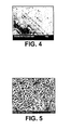
- FIG. 4 is a photomicrograph of a main frame of the display device before surface treatment according to the first embodiment
- FIG. 5 is a photomicrograph of a main frame of the display device after surface treatment according to the first embodiment
- FIG. 6 is a cross-sectional view of the display device having the top case according to the first embodiment.
- FIG. 7 is a top view of the display device according to the first embodiment.
- FIG. 2 is a top view of a top case of a display device according to an example of a first embodiment.
- a top case 100 is made by connecting each metal plate which is separated from each other along the outlines of the top surface of the display device. Therefore, through the opening area 101b of the front surface of the top case 100, the image is displayed.
- the top case 100 has at least one joint portion 101a caused by separated metal plates, the joint portion 101a is firmly combined on the top surfaces of the metal plates by thermoplastic resin using an injection mold method, which completes one top case 100.
- FIG. 3 is a schematic perspective view of the top case of FIG. 2 .
- FIG. 4 is a photomicrograph of a surface of the main frame 102 of the display device before surface treatment according to the first embodiment
- FIG. 5 is a photomicrograph of a surface of the main frame 102 of the display device after surface treatment according to the first embodiment.
- the top case 100 is configured to cover the outlines of top and side surfaces of the display device.
- the sub frame 101 which covers the outlines of the top surface of the display device, has one color and is made of thermoplastic resin.
- the main frame 102 is made of metal and has a patterned design on its surface.
- the sub frame 101 and the main frame 102 are combined by the following processes.
- the surface of the main frame 102 has minute uneven designs.
- the minute uneven designs are formed by a surface treatment process of the main frame 102.
- the surface treatment process includes first and second pretreatment steps.
- the first pretreatment step uses alkaline aqueous solution of 0.1 to 10% concentration, which may include alkali metal hydroxide such as sodium hydroxide, potassium hydroxide and/or anhydrous sodium carbonate or ammonia.
- the second pretreatment step uses acid aqueous solution of 0 to 1 % concentration, which may include acetic acid or hydrofluoric acid.
- the reducing agents may include alkali metal sulfite, alkali metal bisulphate, hydrazine (N 2 H 4 ), sodium boron hydride (NaBH 4 ), lithium aluminum hydride (LiAlH 4 ), and so on.
- the main frame 102 is treated by an aqueous solution selected at least one from ammonia (NH 3 ), hydrazine (N 2 H 4 ), pyridine (C 5 H 5 N), hydrazine derivative, and aqueous amino compounds, which may be called a T-treatment step.
- the solution is of 2 to 30 % concentration.
- the treatment can be done with a gas absorption method, or they can be immersed in the solution, or the solution can be sprayed to them.
- thermo-plastic resin having at least one color is incorporated with the metal material, and the pattern of metal material is shown on the surface of the thermoplastic resin.
- the thermoplastic resin layer has a design. That is, by letting the pattern of the main frame 102 to be seen on the sub frame 101, the bezel area 200b of the display panel can have an improved sense of beauty or aesthetic.
- the thermo-plastic resin may be Nylon (PA6,PA66,PP), polybuthlene terephthalate (PBT), polyphenylene sulfide (PPS), polymethyl methacrylate (PMMA), polycarbonate (PC), which may be used by itself or with organic or inorganic fillers having good coloring characteristics, or with an additive considering strength, thermal resistance, adhesion, electric characteristic.
- Nylon PA6,PA66,PP
- PBT polybuthlene terephthalate
- PPS polyphenylene sulfide
- PMMA polymethyl methacrylate
- PC polycarbonate
- the inorganic filler can be glass fiber, carbon fiber, or metal fiber and the organic filler can be fluoride resin or acrylic resin.
- the additive can be flame retardant, coloring, antioxidant, parting agent, lubricant, or crystal accelerator, and so on according to the required performance.
- pigment or dye is added to the thermoplastic resin.
- the pigment may be carbon black, titan white, chrome yellow, and the dye may be soluble dye such as oil yellow, oil blue, or oil red.
- the top case 100 is completed using four metal plates, but other numbers of the metal plates may be used. That is, this can be applied to top case of various structures, such as the metal plate having at least one joint portion.
- FIG. 6 is a cross-sectional view of the display device having the top case according to the first embodiment.
- the display device has a display area 200a for displaying images, a display panel 200 having a bezel area 200b along the edges of the display area, a backlight unit 300 for supplying light to the display panel 200, supporting members 401 and 402 for supporting the display panel 200 and the backlight unit 300, and the top case 100 combined with the supporting members 401 and 402.
- the top case 100 has the main frame 102 combined with the supporting members 401 and 402, and the sub frame 101 having at least one color and pattern.
- the sub frame 101 is positioned on the bezel area 200b.
- the display panel 200 has upper 201 and lower polarizers 203.
- the lower polarizer 203 selectively transmits linearly-polarized light from the backlight unit 300 to a panel 202 and the upper polarizer 201 selectively transmits linearly-polarized light from the display panel 202 to the outside.
- the supporting members include a main support 401 and a bottom cover 402.
- the main support 401 surrounds and supports a side portion of the display panel 200 and the backlight unit 300.
- the bottom cover 402 covers the bottom portion and the side portion of the main support 401.
- the top case 100 surrounds the main support 401 and the bottom cover 402.
- the main support 401 can be formed by an injection molding method and may have stepped portions.
- the backlight unit 300 is provided at the lowest stepped portion, and the display panel 200 is positioned on the backlight unit 300.
- the top case 100 has the sub frame 101 and the main frame 102, and may surround the top portion and the side portion of the main support 401 to support the display panel 200.
- the sub frame 101 is positioned on the bezel area 200b and covers the top portion and the side portion of the main frame 102, which supports side portion of the display device.
- the main frame 102 can be straight-bar shaped or reversed L shaped.
- the thickness of the sub frame 101 is preferably constant.
- the sub frame 101 of thermoplastic resin has at least one color and a pattern on the bezel area 200b, without any other additional process, as explained above.
- the backlight unit 300 has a lamp housing (not shown) including a light source (not shown), a light guide plate 302 for transferring light from the light source to surface light, optical sheets 301 for increasing the efficiency of the light towards the display panel 200, a reflector 303 for reflecting the light from the light guide plate 302 towards the display panel 200.
- the optical sheets 303 are attached to the light guide plate 302 and the reflector 303 is attached to the bottom surface of the light guide plate 302.
- the light guide plate 302 provides uniform light distribution to the entire display device from the light source.
- the optical sheets 302 include diffusion sheets and prism sheets.
- the optical sheets 302 may diffuse or collimate light passing through the light guide plate 302 to improve uniformity and brightness of the planar light, thereby enlarging the viewing angle.
- a pad 403 is disposed near the main support 401, the position can be changed. For example, it can be positioned on the sides of the top case 100 or bottom cover 402.
- the pad 403 may be a silicon pad for releasing pressure or impact.
- the pad 403 may also protect against dust.
- FIG. 7 is a top view of the display device according to the first embodiment.
- the display device has the display area 200a for display images and the bezel area disposed along the edges of the display area 200a.
- the patterns or designs with an increased sense of beauty can be seen in the bezel area 200b. That is, since the sub frame 101 has at least one color and the patterns of the main frame 102 appear on the sub frame 101, it is possible to form various designs on the bezel area 200b.
Landscapes
- Physics & Mathematics (AREA)
- Nonlinear Science (AREA)
- Crystallography & Structural Chemistry (AREA)
- Chemical & Material Sciences (AREA)
- General Physics & Mathematics (AREA)
- Mathematical Physics (AREA)
- Engineering & Computer Science (AREA)
- Optics & Photonics (AREA)
- Signal Processing (AREA)
- Multimedia (AREA)
- Theoretical Computer Science (AREA)
- Devices For Indicating Variable Information By Combining Individual Elements (AREA)
- Liquid Crystal (AREA)
Abstract
Description
- The invention claims the benefit of Korean Patent Application No.
10-2012-0043877 - The invention relates to a display device, and more particularly, to a display device including a case top with a main frame and a sub frame.
- Display devices encompass all devices for displaying images of display signals from outside, and include monitors receiving signals from personal computers and televisions receiving signals from broadcast stations. The display devices have been developed from cathode ray tubes (CRT) utilizing electrons emitted from the cathode in the vacuum to liquid crystal displays (LCD) utilizing variation of transmission degree of crystals according to the applied voltages, Plasma Display Panels (PDP) utilizing plasma phenomena, and so on. Display devices, such as LCDs and PDPs, have succeeded in accomplishing smaller thicknesses as compared to CRTs. By reducing weight and volume of displays, device size may be increased. In addition, research and development continues for enhancing response speed and display quality.
- In recent years, with effort to technical aspects of the display, technical research for design is desired to attract customers and become one of main concerns. In this aspect, a bezel area between edges of the display panel to the active area for display is determinative.
- Various methods have been suggested to reduce the bezel area and improve its design quality.
FIG. 1 is a cross-sectional view illustrating a liquid crystal display (LCD) device according to the related art. - In
FIG. 1 , thedisplay device 1 has abacklight unit 30 and a liquidcrystal display panel 22. Thebacklight unit 30 and the liquidcrystal display panel 22 are secured by amain support 41, atop case 10, and abottom cover 42. Thetop case 10 is a single unit, and is a reversed L-shaped to cover the top surface and the side edges of the display device. Thetop case 10 defines a rectangular opening portion for displaying images of thedisplay panel 22 and is fixed to themain support 41 or thebottom cover 42. To form the opening portion, it is required to cut a bigger sized metal plate, which increases material cost. Further since thetop case 10 has narrow width, it is not sufficient to reinforce thedisplay device 1. - To solve the above problem, Korean Patent No.
10-1048695 - Accordingly, the present invention is directed to a display device that substantially obviates one or more of the problems due to limitations and disadvantages of the related art.
- An advantage of the present invention is to provide a display device including a bezel area where an improved sense of beauty can be admired.
- Another advantage of the present invention is to provide a display device including separated top cases that are firmly fixed and can protect the display panel with high strength.
- Additional features and advantages of the invention will be set forth in the description which follows, and in part will be apparent from the description, or may be learned by practice of the invention. These and other advantages of the invention will be realized and attained by the structure particularly pointed out in the written description and claims hereof as well as the appended drawings.
- To achieve these and other advantages and in accordance with the purpose of embodiments of the invention, as embodied and broadly described, a display device includes a display panel having a display area and a bezel area formed around edges of the display area; a backlight unit disposed on a rear side of the display panel to provide light to the display panel; a supporting member to support the display panel and the backlight unit; and a top case having at least one joint and incorporated with a surface of the supporting member, wherein the top case has a main frame combined with the supporting member, and a sub frame having a design of at least one color and disposed on the bezel area.
- It is to be understood that both the foregoing general description and the following detailed description are exemplary and explanatory and are intended to provide further explanation of the invention as claimed.
- The accompanying drawings, which are included to provide a further understanding of the invention and are incorporated in and constitute a part of this specification, illustrate embodiments of the invention and together with the description serve to explain the principles of the invention. In the drawings:
-
FIG. 1 is an exploded perspective view of illustrating a display device according to the related art; -
FIG. 2 is a top view of a top case of a display device according to an example of a first embodiment of the present invention; -
FIG. 3 is a schematic perspective view of the top case ofFIG. 2 ; -
FIG. 4 is a photomicrograph of a main frame of the display device before surface treatment according to the first embodiment; -
FIG. 5 is a photomicrograph of a main frame of the display device after surface treatment according to the first embodiment; -
FIG. 6 is a cross-sectional view of the display device having the top case according to the first embodiment; and -
FIG. 7 is a top view of the display device according to the first embodiment. - Reference will now be made in detail to embodiments of the present invention, examples of which are illustrated in the accompanying drawings. Same numerals represent substantially the same element throughout this specification. Concrete explanation of well known structure is omitted for avoiding unnecessary misunderstanding of this invention.
-
FIG. 2 is a top view of a top case of a display device according to an example of a first embodiment. - As shown in
FIG. 2 , atop case 100 is made by connecting each metal plate which is separated from each other along the outlines of the top surface of the display device. Therefore, through theopening area 101b of the front surface of thetop case 100, the image is displayed. - Here, the
top case 100 has at least onejoint portion 101a caused by separated metal plates, thejoint portion 101a is firmly combined on the top surfaces of the metal plates by thermoplastic resin using an injection mold method, which completes onetop case 100. - Therefore, it is possible to lower process cost by reducing wasted metal plates which occur during making the top case with one metal plate. Also, it is possible to prevent foreign substances from entering through the
joint portion 101a of the separated metal plates. -
FIG. 3 is a schematic perspective view of the top case ofFIG. 2 .FIG. 4 is a photomicrograph of a surface of themain frame 102 of the display device before surface treatment according to the first embodiment, andFIG. 5 is a photomicrograph of a surface of themain frame 102 of the display device after surface treatment according to the first embodiment. - As shown in
FIG. 3 , thetop case 100 is configured to cover the outlines of top and side surfaces of the display device. Here, thesub frame 101, which covers the outlines of the top surface of the display device, has one color and is made of thermoplastic resin. Themain frame 102 is made of metal and has a patterned design on its surface. - The
sub frame 101 and themain frame 102 are combined by the following processes. - As shown in
FIG. 5 , the surface of themain frame 102 has minute uneven designs. The minute uneven designs are formed by a surface treatment process of themain frame 102. - The surface treatment process includes first and second pretreatment steps. The first pretreatment step uses alkaline aqueous solution of 0.1 to 10% concentration, which may include alkali metal hydroxide such as sodium hydroxide, potassium hydroxide and/or anhydrous sodium carbonate or ammonia. The second pretreatment step uses acid aqueous solution of 0 to 1 % concentration, which may include acetic acid or hydrofluoric acid.
- Instead of the first and second pretreatment steps, another pretreatment step can be adopted, where an aqueous solution of reducing agents of 1 to 5 % concentration is applied for several minutes. The reducing agents may include alkali metal sulfite, alkali metal bisulphate, hydrazine (N2H4), sodium boron hydride (NaBH4), lithium aluminum hydride (LiAlH4), and so on.
- After the pretreatment steps, the
main frame 102 is treated by an aqueous solution selected at least one from ammonia (NH3), hydrazine (N2H4), pyridine (C5H5N), hydrazine derivative, and aqueous amino compounds, which may be called a T-treatment step. The solution is of 2 to 30 % concentration. The treatment can be done with a gas absorption method, or they can be immersed in the solution, or the solution can be sprayed to them. - Subsequently, a cleaning and drying step is performed.
- Although a surface treatment process is illustrated as explained above, other methods for forming an uneven pattern or design can be adopted.
- In succession, the thermo-plastic resin having at least one color is incorporated with the metal material, and the pattern of metal material is shown on the surface of the thermoplastic resin. Thus, the thermoplastic resin layer has a design. That is, by letting the pattern of the
main frame 102 to be seen on thesub frame 101, thebezel area 200b of the display panel can have an improved sense of beauty or aesthetic. - The thermo-plastic resin may be Nylon (PA6,PA66,PP), polybuthlene terephthalate (PBT), polyphenylene sulfide (PPS), polymethyl methacrylate (PMMA), polycarbonate (PC), which may be used by itself or with organic or inorganic fillers having good coloring characteristics, or with an additive considering strength, thermal resistance, adhesion, electric characteristic.
- For example, the inorganic filler can be glass fiber, carbon fiber, or metal fiber and the organic filler can be fluoride resin or acrylic resin. The additive can be flame retardant, coloring, antioxidant, parting agent, lubricant, or crystal accelerator, and so on according to the required performance.
- Especially, according to the embodiment of the invention, pigment or dye is added to the thermoplastic resin. The pigment may be carbon black, titan white, chrome yellow, and the dye may be soluble dye such as oil yellow, oil blue, or oil red.
- According to this example, the
top case 100 is completed using four metal plates, but other numbers of the metal plates may be used. That is, this can be applied to top case of various structures, such as the metal plate having at least one joint portion. -
FIG. 6 is a cross-sectional view of the display device having the top case according to the first embodiment. As shown inFIG.6 , the display device has adisplay area 200a for displaying images, adisplay panel 200 having abezel area 200b along the edges of the display area, a backlight unit 300 for supplying light to thedisplay panel 200, supportingmembers display panel 200 and the backlight unit 300, and thetop case 100 combined with the supportingmembers top case 100 has themain frame 102 combined with the supportingmembers sub frame 101 having at least one color and pattern. Thesub frame 101 is positioned on thebezel area 200b. - The
display panel 200 has upper 201 andlower polarizers 203. The lower polarizer 203 selectively transmits linearly-polarized light from the backlight unit 300 to apanel 202 and theupper polarizer 201 selectively transmits linearly-polarized light from thedisplay panel 202 to the outside. - The supporting members include a
main support 401 and abottom cover 402. Themain support 401 surrounds and supports a side portion of thedisplay panel 200 and the backlight unit 300. Thebottom cover 402 covers the bottom portion and the side portion of themain support 401. Thetop case 100 surrounds themain support 401 and thebottom cover 402. Themain support 401 can be formed by an injection molding method and may have stepped portions. The backlight unit 300 is provided at the lowest stepped portion, and thedisplay panel 200 is positioned on the backlight unit 300. - The
top case 100 has thesub frame 101 and themain frame 102, and may surround the top portion and the side portion of themain support 401 to support thedisplay panel 200. As shown inFIG. 6 , thesub frame 101 is positioned on thebezel area 200b and covers the top portion and the side portion of themain frame 102, which supports side portion of the display device. Themain frame 102 can be straight-bar shaped or reversed L shaped. - To support the display device firmly, the thickness of the
sub frame 101 is preferably constant. Thesub frame 101 of thermoplastic resin has at least one color and a pattern on thebezel area 200b, without any other additional process, as explained above. - The backlight unit 300 has a lamp housing (not shown) including a light source (not shown), a light guide plate 302 for transferring light from the light source to surface light,
optical sheets 301 for increasing the efficiency of the light towards thedisplay panel 200, areflector 303 for reflecting the light from the light guide plate 302 towards thedisplay panel 200. Theoptical sheets 303 are attached to the light guide plate 302 and thereflector 303 is attached to the bottom surface of the light guide plate 302. - The light guide plate 302 provides uniform light distribution to the entire display device from the light source. The optical sheets 302 include diffusion sheets and prism sheets. The optical sheets 302 may diffuse or collimate light passing through the light guide plate 302 to improve uniformity and brightness of the planar light, thereby enlarging the viewing angle.
- In
FIG. 6 , though apad 403 is disposed near themain support 401, the position can be changed. For example, it can be positioned on the sides of thetop case 100 orbottom cover 402. Thepad 403 may be a silicon pad for releasing pressure or impact. Thepad 403 may also protect against dust. -
FIG. 7 is a top view of the display device according to the first embodiment. The display device has thedisplay area 200a for display images and the bezel area disposed along the edges of thedisplay area 200a. - As explained above, the patterns or designs with an increased sense of beauty can be seen in the
bezel area 200b. That is, since thesub frame 101 has at least one color and the patterns of themain frame 102 appear on thesub frame 101, it is possible to form various designs on thebezel area 200b. - It will be apparent to those skilled in the art that various modifications and variations can be made in the present invention without departing from the spirit or scope of the invention. Thus, it is intended that the present invention cover the modifications and variations of this invention provided that they come within the scope of the appended claims and their equivalents.
Claims (14)
- A display device, comprising:a display panel having a display area and a bezel area formed around edges of the display area;a backlight unit disposed on a rear side of the display panel to provide light to the display panel;a supporting member to support the display panel and the backlight unit; anda top case having at least one joint and incorporated with a surface of the supporting member, wherein the top case has a main frame combined with the supporting member, and a sub frame having a design of at least one color and disposed on the bezel area.
- The device according to claim 1, wherein the main frame includes metal having pattern on a surface thereof, and the sub frame includes a thermoplastic resin.
- The device according to claim 2, wherein the sub frame bonded to the main frame by an injection molded thermoplastic resin.
- The device according to claim 1, wherein the sub frame is bonded to the main frame on the bezel area.
- The device according to claim 1, wherein the sub frame of the top case includes a uniform thickness.
- The device according to claim 1, wherein the supporting member has a bottom cover to accommodate the display panel and the backlight unit, and a main support to fix positions of the display panel and the backlight unit.
- The device according to claim 1, further comprising a pad to absorb impact and to protect the display panel from dust.
- The display device according to claim 1, wherein the main frame of the top case includes a plurality of metal plates connected to each other to surround the display panel and the supporting member.
- The display device according to claim 8, wherein the metal plates are firmly combined by the sub frame formed of a thermoplastic disposed on top surfaces of the metal plates.
- The display device according to claim 8, wherein the connected metal plates define an opening with the display panel disposed in the opening.
- The display device according to claim 1, wherein the sub frame includes a thermoplastic resin.
- The display device according to claim 11, wherein the thermoplastic resin of the sub frame includes the at least one color.
- The display device according to claim 1, wherein the main frame includes a metal.
- The display device according to claim 1, wherein the main frame is straight-bar shaped or a reversed L shape.
Applications Claiming Priority (1)
| Application Number | Priority Date | Filing Date | Title |
|---|---|---|---|
| KR1020120043877A KR101307960B1 (en) | 2012-04-26 | 2012-04-26 | Display device |
Publications (3)
| Publication Number | Publication Date |
|---|---|
| EP2657752A2 true EP2657752A2 (en) | 2013-10-30 |
| EP2657752A3 EP2657752A3 (en) | 2014-09-03 |
| EP2657752B1 EP2657752B1 (en) | 2018-01-10 |
Family
ID=47429502
Family Applications (1)
| Application Number | Title | Priority Date | Filing Date |
|---|---|---|---|
| EP12007996.7A Active EP2657752B1 (en) | 2012-04-26 | 2012-11-28 | Display device |
Country Status (5)
| Country | Link |
|---|---|
| US (1) | US9323083B2 (en) |
| EP (1) | EP2657752B1 (en) |
| KR (1) | KR101307960B1 (en) |
| CN (1) | CN103376573B (en) |
| TW (1) | TWI486672B (en) |
Families Citing this family (7)
| Publication number | Priority date | Publication date | Assignee | Title |
|---|---|---|---|---|
| DE102010063969A1 (en) * | 2010-12-22 | 2012-06-28 | Bayerische Motoren Werke Aktiengesellschaft | Display device for a motor vehicle |
| KR101346083B1 (en) * | 2012-04-26 | 2013-12-31 | 엘지디스플레이 주식회사 | Display Device |
| JP6932926B2 (en) * | 2015-09-18 | 2021-09-08 | 東レ株式会社 | Housing |
| KR102599883B1 (en) * | 2016-11-15 | 2023-11-09 | 삼성전자주식회사 | Display apparatus |
| EP3582208B1 (en) * | 2017-02-09 | 2021-05-26 | Panasonic Intellectual Property Management Co., Ltd. | Image display apparatus |
| KR20180095747A (en) | 2017-02-17 | 2018-08-28 | 희성전자 주식회사 | Middle cabinet and display device having the same |
| US20250138354A1 (en) * | 2021-11-29 | 2025-05-01 | Chengdu Boe Optoelectronics Technology Co., Ltd. | Display frame and display |
Citations (1)
| Publication number | Priority date | Publication date | Assignee | Title |
|---|---|---|---|---|
| KR101048695B1 (en) | 2003-12-12 | 2011-07-14 | 엘지디스플레이 주식회사 | LCD Display |
Family Cites Families (49)
| Publication number | Priority date | Publication date | Assignee | Title |
|---|---|---|---|---|
| US3703431A (en) * | 1971-08-03 | 1972-11-21 | Wayne G Kemper | Decorative plastic wall tile |
| JP3060654B2 (en) * | 1990-12-27 | 2000-07-10 | セイコーエプソン株式会社 | Liquid crystal display |
| JP2538112Y2 (en) * | 1991-05-21 | 1997-06-11 | シャープ株式会社 | Mounting board |
| JPH09147618A (en) * | 1995-11-20 | 1997-06-06 | Sharp Corp | Lighting system |
| KR100453177B1 (en) * | 1998-09-19 | 2005-04-08 | 엘지.필립스 엘시디 주식회사 | Liquid Crystal Display with Black Layer and Fabricating Method Thereof |
| US6654078B1 (en) * | 1999-02-18 | 2003-11-25 | Nec Lcd Technologies, Ltd. | Liquid crystal module mounting structure and mobile terminal mounted with the same |
| KR100603838B1 (en) * | 1999-09-20 | 2006-07-24 | 엘지.필립스 엘시디 주식회사 | Liquid crystal display |
| JP3645770B2 (en) * | 2000-01-28 | 2005-05-11 | 株式会社日立製作所 | Liquid crystal display |
| JP3642263B2 (en) * | 2000-05-23 | 2005-04-27 | セイコーエプソン株式会社 | Liquid crystal device and electronic device |
| KR100757794B1 (en) * | 2001-09-03 | 2007-09-11 | 삼성전자주식회사 | Liquid crystal display module and liquid crystal display device having same |
| KR100442491B1 (en) * | 2001-12-29 | 2004-07-30 | 엘지.필립스 엘시디 주식회사 | Liquid crystal panel and liquid crystal display having same |
| JP2003279935A (en) * | 2002-03-25 | 2003-10-02 | Toshiba Corp | Liquid crystal display |
| CN100373233C (en) * | 2002-03-28 | 2008-03-05 | 三洋电机株式会社 | Liquid crystal display device having a plurality of pixel electrodes |
| KR100946444B1 (en) * | 2002-08-02 | 2010-03-10 | 소니 주식회사 | Flat screen display |
| AU2003277618A1 (en) | 2002-11-08 | 2004-06-07 | Taisei Plas Co., Ltd. | Composite of aluminum alloy and resin composition and process for producing the same |
| TW572220U (en) * | 2003-01-08 | 2004-01-11 | Hannstar Display Corp | Liquid crystal display module and its fixing structure |
| JP4260519B2 (en) * | 2003-03-31 | 2009-04-30 | シャープ株式会社 | Liquid crystal display |
| KR100669700B1 (en) * | 2003-11-28 | 2007-01-16 | 삼성에스디아이 주식회사 | Plasma Display Assembly with Improved Thermal Performance |
| JP3850847B2 (en) * | 2004-06-28 | 2006-11-29 | 株式会社東芝 | Liquid crystal display protection structure for electronic equipment |
| JP4581726B2 (en) * | 2004-12-28 | 2010-11-17 | ソニー株式会社 | Display device and portable device |
| KR101253057B1 (en) * | 2005-07-07 | 2013-04-10 | 삼성디스플레이 주식회사 | Liquid Crystal Display |
| US8031289B2 (en) | 2005-09-22 | 2011-10-04 | Taisei Plas Co., Ltd. | Optical sheet retaining tool and chassis for liquid crystal display device |
| JP4704868B2 (en) * | 2005-09-22 | 2011-06-22 | 大成プラス株式会社 | Chassis frame manufacturing method and chassis frame for large flat display device |
| CN101341023B (en) | 2005-12-08 | 2012-05-30 | 大成普拉斯株式会社 | Composite of aluminum alloy and resin and production method thereof |
| JP5124129B2 (en) * | 2005-12-08 | 2013-01-23 | 東レ株式会社 | Aluminum alloy-resin composite and method for producing the same |
| JP4619979B2 (en) | 2006-04-06 | 2011-01-26 | 東芝モバイルディスプレイ株式会社 | Surface light source device and liquid crystal display device using the same |
| KR101323389B1 (en) * | 2006-12-29 | 2013-10-29 | 엘지디스플레이 주식회사 | backlight unit and display device having the same |
| JP4274249B2 (en) * | 2007-01-16 | 2009-06-03 | エプソンイメージングデバイス株式会社 | Electro-optical device and electronic apparatus |
| CN101589263A (en) * | 2007-04-19 | 2009-11-25 | 夏普株式会社 | Backlight unit and liquid crystal display |
| US8192815B2 (en) * | 2007-07-13 | 2012-06-05 | Apple Inc. | Methods and systems for forming a dual layer housing |
| JP4520494B2 (en) * | 2007-08-20 | 2010-08-04 | 明拓工業株式会社 | Display device |
| BRPI0818466A2 (en) | 2007-10-29 | 2019-09-24 | Sharp Kk | display device |
| KR101431154B1 (en) * | 2007-11-08 | 2014-08-18 | 삼성디스플레이 주식회사 | Display apparatus and method for assembling the same |
| KR101418932B1 (en) | 2007-12-10 | 2014-07-14 | 삼성디스플레이 주식회사 | Display device, upper storage container, and display device assembly method |
| JP4516106B2 (en) | 2007-12-18 | 2010-08-04 | 東芝モバイルディスプレイ株式会社 | Flat display device and manufacturing method thereof |
| JP5504583B2 (en) | 2008-05-30 | 2014-05-28 | 日本電気株式会社 | Electronic device display device fixing structure and electronic device including the structure |
| US8049120B2 (en) * | 2008-09-30 | 2011-11-01 | Apple Inc. | Ultrasonic bonding of discrete plastic parts to metal |
| CN101730410A (en) * | 2008-10-20 | 2010-06-09 | 深圳富泰宏精密工业有限公司 | Shell and manufacture method thereof |
| JP2010134349A (en) * | 2008-12-08 | 2010-06-17 | Sony Corp | Liquid crystal display device |
| US20100159273A1 (en) * | 2008-12-24 | 2010-06-24 | John Benjamin Filson | Method and Apparatus for Forming a Layered Metal Structure with an Anodized Surface |
| KR20110033472A (en) * | 2009-09-25 | 2011-03-31 | 엘지전자 주식회사 | Display |
| US20110089792A1 (en) * | 2009-10-16 | 2011-04-21 | Apple Inc. | Portable computer housing |
| US8858854B2 (en) | 2010-04-01 | 2014-10-14 | Flextronics Ap, Llc | System and method for plastic overmolding on a metal surface |
| TWI440934B (en) * | 2010-04-27 | 2014-06-11 | Lg Display Co Ltd | Display device |
| KR101327743B1 (en) * | 2010-04-27 | 2013-11-11 | 엘지디스플레이 주식회사 | Display apparatus |
| US20120008271A1 (en) * | 2010-07-06 | 2012-01-12 | Dell Products L.P. | Metal laminate via in-mold film |
| KR20120030821A (en) * | 2010-09-20 | 2012-03-29 | 삼성전자주식회사 | Back light unit and liquid crystal display having the same |
| US9280183B2 (en) * | 2011-04-01 | 2016-03-08 | Apple Inc. | Advanced techniques for bonding metal to plastic |
| US8975540B2 (en) * | 2011-12-19 | 2015-03-10 | Htc Corporation | Electronic deviceswith support frames and mechanically-bonded plastic and methods for forming such electronic devices |
-
2012
- 2012-04-26 KR KR1020120043877A patent/KR101307960B1/en not_active Expired - Fee Related
- 2012-11-13 US US13/675,413 patent/US9323083B2/en active Active
- 2012-11-20 CN CN201210470827.XA patent/CN103376573B/en not_active Expired - Fee Related
- 2012-11-28 EP EP12007996.7A patent/EP2657752B1/en active Active
- 2012-12-21 TW TW101149207A patent/TWI486672B/en not_active IP Right Cessation
Patent Citations (1)
| Publication number | Priority date | Publication date | Assignee | Title |
|---|---|---|---|---|
| KR101048695B1 (en) | 2003-12-12 | 2011-07-14 | 엘지디스플레이 주식회사 | LCD Display |
Also Published As
| Publication number | Publication date |
|---|---|
| TW201344292A (en) | 2013-11-01 |
| CN103376573B (en) | 2017-04-05 |
| US20130286624A1 (en) | 2013-10-31 |
| US9323083B2 (en) | 2016-04-26 |
| KR101307960B1 (en) | 2013-09-12 |
| TWI486672B (en) | 2015-06-01 |
| EP2657752A3 (en) | 2014-09-03 |
| EP2657752B1 (en) | 2018-01-10 |
| CN103376573A (en) | 2013-10-30 |
Similar Documents
| Publication | Publication Date | Title |
|---|---|---|
| US9239480B2 (en) | Display device | |
| EP2657752B1 (en) | Display device | |
| JP5536476B2 (en) | Display device | |
| US7667786B2 (en) | Curved liquid-crystal display device and backlight used for curved liquid-crystal display device | |
| US20110261282A1 (en) | Display device | |
| US9366804B2 (en) | Backplane and backlight module and liquid crystal display device using same | |
| US10082693B2 (en) | Display apparatus | |
| TWI402572B (en) | Backlight unit, method for assembling the same and liquid crystal display device using the backlight unit | |
| CN201170823Y (en) | LCD module | |
| US10345649B2 (en) | Concaves for backlight source, display module, and display device | |
| CN201096310Y (en) | Side light type backlight module group structure | |
| CN102932617A (en) | Frame structure device of narrow-frame liquid crystal display television | |
| CN203068333U (en) | Backlight module and display device | |
| CN207557607U (en) | A kind of liquid crystal display die set of ultra-narrow frame | |
| CN101344683B (en) | Display device | |
| KR101694118B1 (en) | Diffuser sheet and back light unit for liquid crystal display device having the same | |
| WO2007018361A1 (en) | Lcd light guiding plate and back light unit and lcd using a thereof | |
| JP3130253U (en) | Backlight module frame | |
| CN100380195C (en) | LCD module | |
| KR20110119039A (en) | Backlight unit of prism sheet and liquid crystal display including the same | |
| CN208691653U (en) | A kind of multimedia interaction all-in-one machine with carrying device | |
| KR20060061058A (en) | Frame coupling structure and liquid crystal display including the same | |
| KR101186041B1 (en) | Backlight unit and liquid crystal display having the same | |
| KR100920810B1 (en) | Scratch-resistant light collecting sheet and backlight unit for liquid crystal display device comprising the same | |
| KR20060028899A (en) | Backlight assembly |
Legal Events
| Date | Code | Title | Description |
|---|---|---|---|
| PUAI | Public reference made under article 153(3) epc to a published international application that has entered the european phase |
Free format text: ORIGINAL CODE: 0009012 |
|
| AK | Designated contracting states |
Kind code of ref document: A2 Designated state(s): AL AT BE BG CH CY CZ DE DK EE ES FI FR GB GR HR HU IE IS IT LI LT LU LV MC MK MT NL NO PL PT RO RS SE SI SK SM TR |
|
| AX | Request for extension of the european patent |
Extension state: BA ME |
|
| 17P | Request for examination filed |
Effective date: 20140321 |
|
| RBV | Designated contracting states (corrected) |
Designated state(s): AL AT BE BG CH CY CZ DE DK EE ES FI FR GB GR HR HU IE IS IT LI LT LU LV MC MK MT NL NO PL PT RO RS SE SI SK SM TR |
|
| PUAL | Search report despatched |
Free format text: ORIGINAL CODE: 0009013 |
|
| AK | Designated contracting states |
Kind code of ref document: A3 Designated state(s): AL AT BE BG CH CY CZ DE DK EE ES FI FR GB GR HR HU IE IS IT LI LT LU LV MC MK MT NL NO PL PT RO RS SE SI SK SM TR |
|
| AX | Request for extension of the european patent |
Extension state: BA ME |
|
| RIC1 | Information provided on ipc code assigned before grant |
Ipc: G02F 1/1333 20060101AFI20140730BHEP Ipc: H04N 5/64 20060101ALI20140730BHEP Ipc: G06F 1/16 20060101ALI20140730BHEP |
|
| GRAP | Despatch of communication of intention to grant a patent |
Free format text: ORIGINAL CODE: EPIDOSNIGR1 |
|
| INTG | Intention to grant announced |
Effective date: 20170803 |
|
| RAP1 | Party data changed (applicant data changed or rights of an application transferred) |
Owner name: LG DISPLAY CO., LTD. |
|
| GRAS | Grant fee paid |
Free format text: ORIGINAL CODE: EPIDOSNIGR3 |
|
| GRAA | (expected) grant |
Free format text: ORIGINAL CODE: 0009210 |
|
| AK | Designated contracting states |
Kind code of ref document: B1 Designated state(s): AL AT BE BG CH CY CZ DE DK EE ES FI FR GB GR HR HU IE IS IT LI LT LU LV MC MK MT NL NO PL PT RO RS SE SI SK SM TR |
|
| REG | Reference to a national code |
Ref country code: CH Ref legal event code: EP Ref country code: AT Ref legal event code: REF Ref document number: 963015 Country of ref document: AT Kind code of ref document: T Effective date: 20180115 |
|
| REG | Reference to a national code |
Ref country code: NL Ref legal event code: FP Ref country code: IE Ref legal event code: FG4D |
|
| REG | Reference to a national code |
Ref country code: DE Ref legal event code: R096 Ref document number: 602012041744 Country of ref document: DE |
|
| REG | Reference to a national code |
Ref country code: AT Ref legal event code: MK05 Ref document number: 963015 Country of ref document: AT Kind code of ref document: T Effective date: 20180110 |
|
| PG25 | Lapsed in a contracting state [announced via postgrant information from national office to epo] |
Ref country code: ES Free format text: LAPSE BECAUSE OF FAILURE TO SUBMIT A TRANSLATION OF THE DESCRIPTION OR TO PAY THE FEE WITHIN THE PRESCRIBED TIME-LIMIT Effective date: 20180110 Ref country code: LT Free format text: LAPSE BECAUSE OF FAILURE TO SUBMIT A TRANSLATION OF THE DESCRIPTION OR TO PAY THE FEE WITHIN THE PRESCRIBED TIME-LIMIT Effective date: 20180110 Ref country code: HR Free format text: LAPSE BECAUSE OF FAILURE TO SUBMIT A TRANSLATION OF THE DESCRIPTION OR TO PAY THE FEE WITHIN THE PRESCRIBED TIME-LIMIT Effective date: 20180110 Ref country code: CY Free format text: LAPSE BECAUSE OF FAILURE TO SUBMIT A TRANSLATION OF THE DESCRIPTION OR TO PAY THE FEE WITHIN THE PRESCRIBED TIME-LIMIT Effective date: 20180110 Ref country code: NO Free format text: LAPSE BECAUSE OF FAILURE TO SUBMIT A TRANSLATION OF THE DESCRIPTION OR TO PAY THE FEE WITHIN THE PRESCRIBED TIME-LIMIT Effective date: 20180410 Ref country code: FI Free format text: LAPSE BECAUSE OF FAILURE TO SUBMIT A TRANSLATION OF THE DESCRIPTION OR TO PAY THE FEE WITHIN THE PRESCRIBED TIME-LIMIT Effective date: 20180110 |
|
| PG25 | Lapsed in a contracting state [announced via postgrant information from national office to epo] |
Ref country code: IS Free format text: LAPSE BECAUSE OF FAILURE TO SUBMIT A TRANSLATION OF THE DESCRIPTION OR TO PAY THE FEE WITHIN THE PRESCRIBED TIME-LIMIT Effective date: 20180510 Ref country code: GR Free format text: LAPSE BECAUSE OF FAILURE TO SUBMIT A TRANSLATION OF THE DESCRIPTION OR TO PAY THE FEE WITHIN THE PRESCRIBED TIME-LIMIT Effective date: 20180411 Ref country code: PL Free format text: LAPSE BECAUSE OF FAILURE TO SUBMIT A TRANSLATION OF THE DESCRIPTION OR TO PAY THE FEE WITHIN THE PRESCRIBED TIME-LIMIT Effective date: 20180110 Ref country code: AT Free format text: LAPSE BECAUSE OF FAILURE TO SUBMIT A TRANSLATION OF THE DESCRIPTION OR TO PAY THE FEE WITHIN THE PRESCRIBED TIME-LIMIT Effective date: 20180110 Ref country code: SE Free format text: LAPSE BECAUSE OF FAILURE TO SUBMIT A TRANSLATION OF THE DESCRIPTION OR TO PAY THE FEE WITHIN THE PRESCRIBED TIME-LIMIT Effective date: 20180110 Ref country code: LV Free format text: LAPSE BECAUSE OF FAILURE TO SUBMIT A TRANSLATION OF THE DESCRIPTION OR TO PAY THE FEE WITHIN THE PRESCRIBED TIME-LIMIT Effective date: 20180110 Ref country code: BG Free format text: LAPSE BECAUSE OF FAILURE TO SUBMIT A TRANSLATION OF THE DESCRIPTION OR TO PAY THE FEE WITHIN THE PRESCRIBED TIME-LIMIT Effective date: 20180410 Ref country code: RS Free format text: LAPSE BECAUSE OF FAILURE TO SUBMIT A TRANSLATION OF THE DESCRIPTION OR TO PAY THE FEE WITHIN THE PRESCRIBED TIME-LIMIT Effective date: 20180110 |
|
| REG | Reference to a national code |
Ref country code: FR Ref legal event code: PLFP Year of fee payment: 7 |
|
| REG | Reference to a national code |
Ref country code: DE Ref legal event code: R097 Ref document number: 602012041744 Country of ref document: DE |
|
| PG25 | Lapsed in a contracting state [announced via postgrant information from national office to epo] |
Ref country code: EE Free format text: LAPSE BECAUSE OF FAILURE TO SUBMIT A TRANSLATION OF THE DESCRIPTION OR TO PAY THE FEE WITHIN THE PRESCRIBED TIME-LIMIT Effective date: 20180110 Ref country code: AL Free format text: LAPSE BECAUSE OF FAILURE TO SUBMIT A TRANSLATION OF THE DESCRIPTION OR TO PAY THE FEE WITHIN THE PRESCRIBED TIME-LIMIT Effective date: 20180110 Ref country code: RO Free format text: LAPSE BECAUSE OF FAILURE TO SUBMIT A TRANSLATION OF THE DESCRIPTION OR TO PAY THE FEE WITHIN THE PRESCRIBED TIME-LIMIT Effective date: 20180110 Ref country code: IT Free format text: LAPSE BECAUSE OF FAILURE TO SUBMIT A TRANSLATION OF THE DESCRIPTION OR TO PAY THE FEE WITHIN THE PRESCRIBED TIME-LIMIT Effective date: 20180110 |
|
| PLBE | No opposition filed within time limit |
Free format text: ORIGINAL CODE: 0009261 |
|
| STAA | Information on the status of an ep patent application or granted ep patent |
Free format text: STATUS: NO OPPOSITION FILED WITHIN TIME LIMIT |
|
| PG25 | Lapsed in a contracting state [announced via postgrant information from national office to epo] |
Ref country code: DK Free format text: LAPSE BECAUSE OF FAILURE TO SUBMIT A TRANSLATION OF THE DESCRIPTION OR TO PAY THE FEE WITHIN THE PRESCRIBED TIME-LIMIT Effective date: 20180110 Ref country code: CZ Free format text: LAPSE BECAUSE OF FAILURE TO SUBMIT A TRANSLATION OF THE DESCRIPTION OR TO PAY THE FEE WITHIN THE PRESCRIBED TIME-LIMIT Effective date: 20180110 Ref country code: SM Free format text: LAPSE BECAUSE OF FAILURE TO SUBMIT A TRANSLATION OF THE DESCRIPTION OR TO PAY THE FEE WITHIN THE PRESCRIBED TIME-LIMIT Effective date: 20180110 Ref country code: SK Free format text: LAPSE BECAUSE OF FAILURE TO SUBMIT A TRANSLATION OF THE DESCRIPTION OR TO PAY THE FEE WITHIN THE PRESCRIBED TIME-LIMIT Effective date: 20180110 |
|
| 26N | No opposition filed |
Effective date: 20181011 |
|
| PG25 | Lapsed in a contracting state [announced via postgrant information from national office to epo] |
Ref country code: SI Free format text: LAPSE BECAUSE OF FAILURE TO SUBMIT A TRANSLATION OF THE DESCRIPTION OR TO PAY THE FEE WITHIN THE PRESCRIBED TIME-LIMIT Effective date: 20180110 |
|
| REG | Reference to a national code |
Ref country code: CH Ref legal event code: PL |
|
| PG25 | Lapsed in a contracting state [announced via postgrant information from national office to epo] |
Ref country code: LU Free format text: LAPSE BECAUSE OF NON-PAYMENT OF DUE FEES Effective date: 20181128 Ref country code: MC Free format text: LAPSE BECAUSE OF FAILURE TO SUBMIT A TRANSLATION OF THE DESCRIPTION OR TO PAY THE FEE WITHIN THE PRESCRIBED TIME-LIMIT Effective date: 20180110 |
|
| REG | Reference to a national code |
Ref country code: BE Ref legal event code: MM Effective date: 20181130 |
|
| REG | Reference to a national code |
Ref country code: IE Ref legal event code: MM4A |
|
| PG25 | Lapsed in a contracting state [announced via postgrant information from national office to epo] |
Ref country code: LI Free format text: LAPSE BECAUSE OF NON-PAYMENT OF DUE FEES Effective date: 20181130 Ref country code: CH Free format text: LAPSE BECAUSE OF NON-PAYMENT OF DUE FEES Effective date: 20181130 |
|
| PG25 | Lapsed in a contracting state [announced via postgrant information from national office to epo] |
Ref country code: IE Free format text: LAPSE BECAUSE OF NON-PAYMENT OF DUE FEES Effective date: 20181128 |
|
| PG25 | Lapsed in a contracting state [announced via postgrant information from national office to epo] |
Ref country code: BE Free format text: LAPSE BECAUSE OF NON-PAYMENT OF DUE FEES Effective date: 20181130 |
|
| PG25 | Lapsed in a contracting state [announced via postgrant information from national office to epo] |
Ref country code: MT Free format text: LAPSE BECAUSE OF NON-PAYMENT OF DUE FEES Effective date: 20181128 |
|
| PG25 | Lapsed in a contracting state [announced via postgrant information from national office to epo] |
Ref country code: TR Free format text: LAPSE BECAUSE OF FAILURE TO SUBMIT A TRANSLATION OF THE DESCRIPTION OR TO PAY THE FEE WITHIN THE PRESCRIBED TIME-LIMIT Effective date: 20180110 |
|
| PG25 | Lapsed in a contracting state [announced via postgrant information from national office to epo] |
Ref country code: PT Free format text: LAPSE BECAUSE OF FAILURE TO SUBMIT A TRANSLATION OF THE DESCRIPTION OR TO PAY THE FEE WITHIN THE PRESCRIBED TIME-LIMIT Effective date: 20180110 |
|
| PG25 | Lapsed in a contracting state [announced via postgrant information from national office to epo] |
Ref country code: MK Free format text: LAPSE BECAUSE OF NON-PAYMENT OF DUE FEES Effective date: 20180110 Ref country code: HU Free format text: LAPSE BECAUSE OF FAILURE TO SUBMIT A TRANSLATION OF THE DESCRIPTION OR TO PAY THE FEE WITHIN THE PRESCRIBED TIME-LIMIT; INVALID AB INITIO Effective date: 20121128 |
|
| PGFP | Annual fee paid to national office [announced via postgrant information from national office to epo] |
Ref country code: NL Payment date: 20250922 Year of fee payment: 14 |
|
| PGFP | Annual fee paid to national office [announced via postgrant information from national office to epo] |
Ref country code: GB Payment date: 20250922 Year of fee payment: 14 |
|
| PGFP | Annual fee paid to national office [announced via postgrant information from national office to epo] |
Ref country code: FR Payment date: 20250925 Year of fee payment: 14 |
|
| PGFP | Annual fee paid to national office [announced via postgrant information from national office to epo] |
Ref country code: DE Payment date: 20250922 Year of fee payment: 14 |