EP2657315A2 - Organic light-emitting device and method for manufacturing same - Google Patents
Organic light-emitting device and method for manufacturing same Download PDFInfo
- Publication number
- EP2657315A2 EP2657315A2 EP11850159.2A EP11850159A EP2657315A2 EP 2657315 A2 EP2657315 A2 EP 2657315A2 EP 11850159 A EP11850159 A EP 11850159A EP 2657315 A2 EP2657315 A2 EP 2657315A2
- Authority
- EP
- European Patent Office
- Prior art keywords
- group
- substituted
- unsubstituted
- carbon atoms
- light emitting
- Prior art date
- Legal status (The legal status is an assumption and is not a legal conclusion. Google has not performed a legal analysis and makes no representation as to the accuracy of the status listed.)
- Granted
Links
- 0 CC1=C*=CC2=CC=CCC12 Chemical compound CC1=C*=CC2=CC=CCC12 0.000 description 22
- DUKGZFKWAMMALZ-MPKXBFJISA-N C/C=C(/C1=CC2c3ccccc3-c3nc(CCC=C4)c4[n]3C2C=C1)\N=C(\C1=NC=CCC1C(C)=C1)/C1=C Chemical compound C/C=C(/C1=CC2c3ccccc3-c3nc(CCC=C4)c4[n]3C2C=C1)\N=C(\C1=NC=CCC1C(C)=C1)/C1=C DUKGZFKWAMMALZ-MPKXBFJISA-N 0.000 description 1
- LQAVKSJAAMAHGJ-YCDFTOKFSA-N C/C=C\C=C(/C)\[n]1c(C(/C=C(/C=CC(c(cc2)cc3c2c2nc(-c4ccccc4C4C=CC=CC44)c4[n]2c2ccccc32)=C2)\C2=C/C)=C)nc2c1cccc2 Chemical compound C/C=C\C=C(/C)\[n]1c(C(/C=C(/C=CC(c(cc2)cc3c2c2nc(-c4ccccc4C4C=CC=CC44)c4[n]2c2ccccc32)=C2)\C2=C/C)=C)nc2c1cccc2 LQAVKSJAAMAHGJ-YCDFTOKFSA-N 0.000 description 1
- GEUNHTHMYKHYPZ-VWNDGZFJSA-N C/C=C\[I]=C(/C)\c1c(-c2ccccc2)nc(-c(cc2)ccc2-c(cc2)cc3c2c2ccccc2[n]2c3nc3c2cccc3)[n]1-c1ccccc1 Chemical compound C/C=C\[I]=C(/C)\c1c(-c2ccccc2)nc(-c(cc2)ccc2-c(cc2)cc3c2c2ccccc2[n]2c3nc3c2cccc3)[n]1-c1ccccc1 GEUNHTHMYKHYPZ-VWNDGZFJSA-N 0.000 description 1
- YUKKWWZXZDSEAE-UTCJRWHESA-N C/C=C\c1c(C)nc2[n]1c(C=C(CC1)C#N)c1c1c2ccc(-c(cc2)ccc2-c2cc(cccc3)c3cc2)c1 Chemical compound C/C=C\c1c(C)nc2[n]1c(C=C(CC1)C#N)c1c1c2ccc(-c(cc2)ccc2-c2cc(cccc3)c3cc2)c1 YUKKWWZXZDSEAE-UTCJRWHESA-N 0.000 description 1
- WYODXBJHTTYIKN-UHFFFAOYSA-N C/C=[I]\c(nc1-c2ccc(cc(cc3)-c(cc45)ccc4c(cccc4)c4[n]4c5nc5c4cccc5)c3c2)c(C)[n]1-c1ccccc1 Chemical compound C/C=[I]\c(nc1-c2ccc(cc(cc3)-c(cc45)ccc4c(cccc4)c4[n]4c5nc5c4cccc5)c3c2)c(C)[n]1-c1ccccc1 WYODXBJHTTYIKN-UHFFFAOYSA-N 0.000 description 1
- QSOUCOVXGRSCSU-UHFFFAOYSA-N C1C=CC=CC1c1c(-c2ccccc2)[n]2c(C=C(C(C=C3)=CC=[IH]3c3nc(cccc4)c4[n]3-c3ccccc3)[I]=C3)c3c3ccccc3c2n1 Chemical compound C1C=CC=CC1c1c(-c2ccccc2)[n]2c(C=C(C(C=C3)=CC=[IH]3c3nc(cccc4)c4[n]3-c3ccccc3)[I]=C3)c3c3ccccc3c2n1 QSOUCOVXGRSCSU-UHFFFAOYSA-N 0.000 description 1
- GTRDQEUYVSCDTH-IKHBIVHXSA-N CC(C)/C=C\C=C/C(N(c(cc(cc1)-[n]2c([F]=CC=C3)c3c3ccccc23)c1C1=C2CCC(C3=C[I]=CC=C3)=C1)C2=N)=C Chemical compound CC(C)/C=C\C=C/C(N(c(cc(cc1)-[n]2c([F]=CC=C3)c3c3ccccc23)c1C1=C2CCC(C3=C[I]=CC=C3)=C1)C2=N)=C GTRDQEUYVSCDTH-IKHBIVHXSA-N 0.000 description 1
- NPHDIYVHDYUZNI-GXHLCREISA-N CC1=[IH](/C=C\C=[IH])c(cc(cc2)C(C=C3)=CCC3c3ccccc3)c2-[n]2c1nc1c2cccc1 Chemical compound CC1=[IH](/C=C\C=[IH])c(cc(cc2)C(C=C3)=CCC3c3ccccc3)c2-[n]2c1nc1c2cccc1 NPHDIYVHDYUZNI-GXHLCREISA-N 0.000 description 1
- WLDPCDRXSDHIDS-DONMJRKJSA-N CC1C(C=CCC2)=C2c2nc(cccc3)c3[n]2C/C=C\C(\c2ccccc2)=C1 Chemical compound CC1C(C=CCC2)=C2c2nc(cccc3)c3[n]2C/C=C\C(\c2ccccc2)=C1 WLDPCDRXSDHIDS-DONMJRKJSA-N 0.000 description 1
- TZSIBCVAQAVEAT-YWYQVNFNSA-N CCc(c1c2C=C[C@@H]3C1=C3)c(/C=C\C)[n]1c2nc(/C=C/c2c(cccc3)c3c(C3=CC4=CC=[IH]=C4C=C3)c3c2CCC2C3=C2)c1C=[IH] Chemical compound CCc(c1c2C=C[C@@H]3C1=C3)c(/C=C\C)[n]1c2nc(/C=C/c2c(cccc3)c3c(C3=CC4=CC=[IH]=C4C=C3)c3c2CCC2C3=C2)c1C=[IH] TZSIBCVAQAVEAT-YWYQVNFNSA-N 0.000 description 1
- IKLJNVIFHDQJKG-UHFFFAOYSA-N Cc1ccccc1-[n]1c(-c(cc2)ccc2-c(cc2)cc3c2c2ccccc2[n]2c3nc3c2cccc3)nc2c(cccc3)c3c(cccc3)c3c12 Chemical compound Cc1ccccc1-[n]1c(-c(cc2)ccc2-c(cc2)cc3c2c2ccccc2[n]2c3nc3c2cccc3)nc2c(cccc3)c3c(cccc3)c3c12 IKLJNVIFHDQJKG-UHFFFAOYSA-N 0.000 description 1
- LZDPWWDSKMRTRR-UHFFFAOYSA-N Ic1ccccc1-c(ccc(-c1ccccn1)c1)c1-c1nc(cccc2)c2[nH]1 Chemical compound Ic1ccccc1-c(ccc(-c1ccccn1)c1)c1-c1nc(cccc2)c2[nH]1 LZDPWWDSKMRTRR-UHFFFAOYSA-N 0.000 description 1
- UHDKQNKYZUIXRS-UHFFFAOYSA-N c(cc1)ccc1-c(cc1)cc(c2ccc(cccc3)c3c22)c1[n]2-c(cc1)cc(c2c3cccc2)c1[n]1c3nc2c1cccc2 Chemical compound c(cc1)ccc1-c(cc1)cc(c2ccc(cccc3)c3c22)c1[n]2-c(cc1)cc(c2c3cccc2)c1[n]1c3nc2c1cccc2 UHDKQNKYZUIXRS-UHFFFAOYSA-N 0.000 description 1
- IERZDMQOFXPYLJ-UHFFFAOYSA-N c(cc12)ccc1nc(c(cc1)c3cc1-c(cc1)ccc1-c1nc4ccccc4[o]1)[n]2c1c3nccc1 Chemical compound c(cc12)ccc1nc(c(cc1)c3cc1-c(cc1)ccc1-c1nc4ccccc4[o]1)[n]2c1c3nccc1 IERZDMQOFXPYLJ-UHFFFAOYSA-N 0.000 description 1
Images


Classifications
-
- H—ELECTRICITY
- H10—SEMICONDUCTOR DEVICES; ELECTRIC SOLID-STATE DEVICES NOT OTHERWISE PROVIDED FOR
- H10K—ORGANIC ELECTRIC SOLID-STATE DEVICES
- H10K85/00—Organic materials used in the body or electrodes of devices covered by this subclass
- H10K85/60—Organic compounds having low molecular weight
- H10K85/649—Aromatic compounds comprising a hetero atom
- H10K85/657—Polycyclic condensed heteroaromatic hydrocarbons
- H10K85/6572—Polycyclic condensed heteroaromatic hydrocarbons comprising only nitrogen in the heteroaromatic polycondensed ring system, e.g. phenanthroline or carbazole
-
- C—CHEMISTRY; METALLURGY
- C07—ORGANIC CHEMISTRY
- C07C—ACYCLIC OR CARBOCYCLIC COMPOUNDS
- C07C15/00—Cyclic hydrocarbons containing only six-membered aromatic rings as cyclic parts
- C07C15/20—Polycyclic condensed hydrocarbons
- C07C15/27—Polycyclic condensed hydrocarbons containing three rings
- C07C15/28—Anthracenes
-
- C—CHEMISTRY; METALLURGY
- C09—DYES; PAINTS; POLISHES; NATURAL RESINS; ADHESIVES; COMPOSITIONS NOT OTHERWISE PROVIDED FOR; APPLICATIONS OF MATERIALS NOT OTHERWISE PROVIDED FOR
- C09K—MATERIALS FOR MISCELLANEOUS APPLICATIONS, NOT PROVIDED FOR ELSEWHERE
- C09K11/00—Luminescent materials, e.g. electroluminescent or chemiluminescent
- C09K11/06—Luminescent materials, e.g. electroluminescent or chemiluminescent containing organic luminescent materials
-
- H—ELECTRICITY
- H05—ELECTRIC TECHNIQUES NOT OTHERWISE PROVIDED FOR
- H05B—ELECTRIC HEATING; ELECTRIC LIGHT SOURCES NOT OTHERWISE PROVIDED FOR; CIRCUIT ARRANGEMENTS FOR ELECTRIC LIGHT SOURCES, IN GENERAL
- H05B33/00—Electroluminescent light sources
- H05B33/12—Light sources with substantially two-dimensional [2D] radiating surfaces
- H05B33/14—Light sources with substantially two-dimensional [2D] radiating surfaces characterised by the chemical or physical composition or the arrangement of the electroluminescent material, or by the simultaneous addition of the electroluminescent material in or onto the light source
-
- H—ELECTRICITY
- H10—SEMICONDUCTOR DEVICES; ELECTRIC SOLID-STATE DEVICES NOT OTHERWISE PROVIDED FOR
- H10K—ORGANIC ELECTRIC SOLID-STATE DEVICES
- H10K50/00—Organic light-emitting devices
- H10K50/10—OLEDs or polymer light-emitting diodes [PLED]
- H10K50/11—OLEDs or polymer light-emitting diodes [PLED] characterised by the electroluminescent [EL] layers
-
- H—ELECTRICITY
- H10—SEMICONDUCTOR DEVICES; ELECTRIC SOLID-STATE DEVICES NOT OTHERWISE PROVIDED FOR
- H10K—ORGANIC ELECTRIC SOLID-STATE DEVICES
- H10K50/00—Organic light-emitting devices
- H10K50/10—OLEDs or polymer light-emitting diodes [PLED]
- H10K50/11—OLEDs or polymer light-emitting diodes [PLED] characterised by the electroluminescent [EL] layers
- H10K50/125—OLEDs or polymer light-emitting diodes [PLED] characterised by the electroluminescent [EL] layers specially adapted for multicolour light emission, e.g. for emitting white light
- H10K50/13—OLEDs or polymer light-emitting diodes [PLED] characterised by the electroluminescent [EL] layers specially adapted for multicolour light emission, e.g. for emitting white light comprising stacked EL layers within one EL unit
-
- H—ELECTRICITY
- H10—SEMICONDUCTOR DEVICES; ELECTRIC SOLID-STATE DEVICES NOT OTHERWISE PROVIDED FOR
- H10K—ORGANIC ELECTRIC SOLID-STATE DEVICES
- H10K85/00—Organic materials used in the body or electrodes of devices covered by this subclass
- H10K85/60—Organic compounds having low molecular weight
- H10K85/631—Amine compounds having at least two aryl rest on at least one amine-nitrogen atom, e.g. triphenylamine
- H10K85/636—Amine compounds having at least two aryl rest on at least one amine-nitrogen atom, e.g. triphenylamine comprising heteroaromatic hydrocarbons as substituents on the nitrogen atom
-
- H—ELECTRICITY
- H10—SEMICONDUCTOR DEVICES; ELECTRIC SOLID-STATE DEVICES NOT OTHERWISE PROVIDED FOR
- H10K—ORGANIC ELECTRIC SOLID-STATE DEVICES
- H10K85/00—Organic materials used in the body or electrodes of devices covered by this subclass
- H10K85/60—Organic compounds having low molecular weight
- H10K85/649—Aromatic compounds comprising a hetero atom
- H10K85/657—Polycyclic condensed heteroaromatic hydrocarbons
-
- C—CHEMISTRY; METALLURGY
- C09—DYES; PAINTS; POLISHES; NATURAL RESINS; ADHESIVES; COMPOSITIONS NOT OTHERWISE PROVIDED FOR; APPLICATIONS OF MATERIALS NOT OTHERWISE PROVIDED FOR
- C09K—MATERIALS FOR MISCELLANEOUS APPLICATIONS, NOT PROVIDED FOR ELSEWHERE
- C09K2211/00—Chemical nature of organic luminescent or tenebrescent compounds
- C09K2211/10—Non-macromolecular compounds
- C09K2211/1003—Carbocyclic compounds
- C09K2211/1007—Non-condensed systems
-
- C—CHEMISTRY; METALLURGY
- C09—DYES; PAINTS; POLISHES; NATURAL RESINS; ADHESIVES; COMPOSITIONS NOT OTHERWISE PROVIDED FOR; APPLICATIONS OF MATERIALS NOT OTHERWISE PROVIDED FOR
- C09K—MATERIALS FOR MISCELLANEOUS APPLICATIONS, NOT PROVIDED FOR ELSEWHERE
- C09K2211/00—Chemical nature of organic luminescent or tenebrescent compounds
- C09K2211/10—Non-macromolecular compounds
- C09K2211/1003—Carbocyclic compounds
- C09K2211/1011—Condensed systems
-
- C—CHEMISTRY; METALLURGY
- C09—DYES; PAINTS; POLISHES; NATURAL RESINS; ADHESIVES; COMPOSITIONS NOT OTHERWISE PROVIDED FOR; APPLICATIONS OF MATERIALS NOT OTHERWISE PROVIDED FOR
- C09K—MATERIALS FOR MISCELLANEOUS APPLICATIONS, NOT PROVIDED FOR ELSEWHERE
- C09K2211/00—Chemical nature of organic luminescent or tenebrescent compounds
- C09K2211/10—Non-macromolecular compounds
- C09K2211/1003—Carbocyclic compounds
- C09K2211/1014—Carbocyclic compounds bridged by heteroatoms, e.g. N, P, Si or B
-
- C—CHEMISTRY; METALLURGY
- C09—DYES; PAINTS; POLISHES; NATURAL RESINS; ADHESIVES; COMPOSITIONS NOT OTHERWISE PROVIDED FOR; APPLICATIONS OF MATERIALS NOT OTHERWISE PROVIDED FOR
- C09K—MATERIALS FOR MISCELLANEOUS APPLICATIONS, NOT PROVIDED FOR ELSEWHERE
- C09K2211/00—Chemical nature of organic luminescent or tenebrescent compounds
- C09K2211/10—Non-macromolecular compounds
- C09K2211/1018—Heterocyclic compounds
- C09K2211/1025—Heterocyclic compounds characterised by ligands
- C09K2211/1029—Heterocyclic compounds characterised by ligands containing one nitrogen atom as the heteroatom
-
- C—CHEMISTRY; METALLURGY
- C09—DYES; PAINTS; POLISHES; NATURAL RESINS; ADHESIVES; COMPOSITIONS NOT OTHERWISE PROVIDED FOR; APPLICATIONS OF MATERIALS NOT OTHERWISE PROVIDED FOR
- C09K—MATERIALS FOR MISCELLANEOUS APPLICATIONS, NOT PROVIDED FOR ELSEWHERE
- C09K2211/00—Chemical nature of organic luminescent or tenebrescent compounds
- C09K2211/10—Non-macromolecular compounds
- C09K2211/1018—Heterocyclic compounds
- C09K2211/1025—Heterocyclic compounds characterised by ligands
- C09K2211/1044—Heterocyclic compounds characterised by ligands containing two nitrogen atoms as heteroatoms
Definitions
- the present invention relates to a heat emitting body and a method for manufacturing the same. More particularly, the present invention relates to a heat emitting body in which heat emitting occurs uniformly and a field of vision is not obstructed, and a method for manufacturing the same.
- This application claims priority from Korean Patent Application No. 10-2010-0134759 filed December 24, 2010 at the KIPO, the disclosure of which is incorporated herein by reference in its entirety.
- An organic light emission phenomenon is an example of converting current into visible rays through an internal process of a specific organic molecule.
- the principle of the organic light emission phenomenon is based on the following mechanism.
- An organic light emitting device using this principle may typically comprise a cathode, an anode, and an organic material layer, for example, an organic material layer comprising a hole injection layer, a hole transporting layer, a light emitting layer, and an electron transporting layer, disposed therebetween.
- the materials used in the organic light emitting device are mostly pure organic materials or complexes of organic materials with metals, and may be classified as a hole injection material, a hole transporting material, a light emitting material, an electron transporting material, or an electron injection material, according to their use.
- an organic material having a p-type property which is easily oxidized and is electrochemically stable when it is oxidized, is usually used as the hole injection material or the hole transporting material.
- an organic material having an n-type property which is easily reduced and is electrochemically stable when it is reduced, is usually used as the electron injection material or the electron transporting material.
- the light emitting layer material an organic material having both p-type and n-type properties is preferable, which is stable when it is oxidized and reduced.
- a material having high light emitting efficiency for converting the exciton into light is preferable.
- the material used in the organic light emitting device further has the following properties.
- the material used in the organic light emitting device has excellent thermal stability. This is due to joule heat generated by movement of electric charges in the organic light emitting device.
- NPB which has currently been used as the hole transporting layer material, has a glass transition temperature of 100°C or less, and thus it is difficult to apply NPB to an organic light emitting device requiring a high current.
- the stability of the material itself is important, and since the OLED device is a device which provides electricity to generate light, the stability for electric charges is important. This means that when a phenomenon in which electrons are introduced into or emitted from a material is repeated, the material itself is not modified or broken.
- a LUMO energy level of PEDOT:PSS which is currently used as a hole transporting material of an organic light emitting device manufactured by using a solution coating method, is lower than that of an organic material used as a light emitting layer material, and thus it is difficult to manufacture an organic light emitting device having high efficiency and a long service life.
- the material used in the organic light emitting device needs to have excellent chemical stability, electric charge mobility, and interfacial characteristic with an electrode or an adjacent layer. That is, the material used in the organic light emitting device needs to be minimally deformed by moisture or oxygen. Furthermore, a proper hole or electron mobility needs to be assured so as to balance densities of the holes and of the electrons in the light emitting layer of the organic light emitting device to maximize the formation of excitons. Additionally, it needs to be able to have a good interface with an electrode comprising metal or metal oxides so as to assure stability of the device.
- materials constituting the organic material layer in the device for example, a hole injection material, a hole transporting material, a light emitting material, an electron transporting material, an electron injection material, and the like need to be supported by stable and efficient materials above anything else, but the development of stable and efficient organic layer materials for organic light emitting device has not been sufficiently achieved. Accordingly, it is necessary to conduct continuous studies on organic light emitting devices.
- An exemplary embodiment of the present invention provides an organic light emitting device, comprising: an anode; a cathode; and an organic material layer of one or more layers disposed between the anode and the cathode, wherein the organic material layer comprises a light emitting layer, and an organic material layer comprising a compound having a fluorescent light emitting efficiency equal to or greater than the fluorescent light emitting efficiency of NPB is positioned between the anode and the light emitting layer.
- an organic light emitting device having high light emitting efficiency and excellent service life by suppressing self-light emitting effects of a hole injection material or a hole transporting material generated when a hole injection layer or a hole transporting layer with high fluorescent light emitting efficiency is in contact with the light emitting layer.
- hole injection and transporting materials have been developed toward increasing the size of an aryl group of a compound. If a region that the aryl group occupies in a molecule is increased, the overlapping region of the p-orbital is widened, and thus an electrically stable material with minimal change in properties due to the in-and-out of electric charges may be produced. Further, the molecular weight of the molecule itself is increased and thus thermal properties which are endured at high deposition temperature or driving temperature also become excellent.
- the fluorescence quantum efficiency refers to a degree in which light is emitted when excitation is produced by an external light or electric charge, and then the state is stabilized to a bottom state. It is natural that light emitting materials having excellent quantum efficiency have excellent properties because the light emitting materials are materials for emitting light. However, hole injection and transporting materials rather serve to deteriorate properties of a device.
- NPB which is mostly used as a hole transporting material
- a paper released by Shumei Liu, et al., (Applied Physics Letters, 97, 083304, 2010 ) disclosed that another material layer was comprised between NPB as a hole transporting layer and a light emitting layer so as to prevent the deterioration of properties of a device by light emission of NPB which was in contact with the light emitting layer, and in this case, properties had been improved by 1.6 times in terms of luminance, compared to a device in which NPB was in direct contact with the light emitting layer.
- the above-exemplified two cases all show methods for improving properties by inserting another material layer between the light emitting layer and the hole transporting layer in order to solve the following problem that when hole injection and transporting materials which have excellent fluorescence quantum efficiency are in contact with the light emitting layer, electric charges (electrons and holes) injected from the anode and the cathode fail to be converted into light in the light emitting layer, are transferred to a hole injection or transporting material layer, which is in contact with the light emitting layer, and contribute to the light emission of a hole injection or transporting material, which deteriorates characteristics of a device.
- the organic light emitting device comprises an anode, a cathode, and an organic material layer of one or more layers disposed between the anode and the cathode, wherein the organic material layer comprises a light emitting layer, and an organic material layer comprising a compound having a fluorescent light emitting efficiency equal to or greater than the fluorescent light emitting efficiency of NPB is positioned between the anode and the light emitting layer.
- the compound having a fluorescent light emitting efficiency equal to or greater than the fluorescent light emitting efficiency of NPB means a compound in which an intensity of the PL (photoluminescence) spectrum at the Max. peak position is equal to or greater than that of the PL spectrum of NPB at the Max. peak position, produced from 350 nm to 500 nm after the same UV wavelength is irradiated in terms of NPB.
- a ratio at which photons or electrons in a material are converted into photons or electrons having different energy levels, and particularly converted into photons is referred to as a light emitting efficiency.
- fluorescent light emitting efficiency has few cases where an organic material applied to a hole transporting layer has a phosphorous light emission, and means that photons irradiated by UV are converted into other photons by materials to release PL.
- UV it is preferable for UV to be irradiated as a light source because the energy band of UV is so great that electrons at a bottom state are sufficiently excited even though the energy gap is different for each organic material, and the excited electrons may be returned to the bottom state to emit photons. Although electrons are excited, whether photons are produced, the amount of photons produced, and the like are inherent properties of a material. Thus, in consideration of a PL efficiency measured by irradiating the same light source, it may be determined which side has a relatively higher or lower fluorescent light emitting efficiency rather than not using an absolute value.
- the fluorescent light emitting efficiency may be measured by using methods known in the art.
- the fluorescent light emitting efficiency may be measured under conditions of a temperature range of 15 to 30°C and a humidity of 70% or less by depositing an organic material layer onto a substrate such as glass, and the like, and then using a measuring apparatus which will be described below, but the method is not limited thereto.
- the excitation wavelength, the fluorescent light emitting efficiency measurement range, the increment, and the integration time may be 350 nm, 350 to 600 nm, 0.5 nm, and 0.5 s, respectively, but are limited thereto.
- the measuring apparatus may comprise Fluorolog-3 spectrofluorometer System, Single-grating excitation spectrometer, TBX-04-A-Single Photon detection module, and the like from HORIBA Jobin Yvon, Inc., but are not limited thereto. Measuring conditions of the fluorescent light emitting efficiency may be appropriately controlled by those skilled in the art depending on a measuring device.
- the organic material layer comprising the compound having a fluorescent light emitting efficiency equal to or greater than that of NPB is preferably in contact with the light emitting layer.
- the present invention may provide an organic light emitting device which suppresses the self-light emission effects of a hole injection material or a hole transporting material to have a high light emitting efficiency and excellent service life by comprising an organic material layer which comprises the compound having the fluorescent light emitting efficiency equal to or greater than that of NPB as a hole injection layer or a hole transporting layer, and comprising the organic material layer which comprises the compound having the fluorescent light emitting efficiency equal to or greater than that of NPB to be in contact with the light emitting layer.
- the organic light emitting device may comprise an organic material layer comprising one or more selected from the group consisting of compounds represented by the following Formulas 1 to 4 between the cathode and the light emitting layer.
- R1, R2, R3, R4, and R5 are the same as or different from each other, and are each independently selected from the group consisting of a hydrogen, an alkyl group having 1 to 10 carbon atoms, an alkenyl group having 2 to 10 carbon atoms, an aryl group having 6 to 20 carbon atoms, and a heteroaryl group having 5 to 20 carbon atoms, except that both of R1 and R2 are a hydrogen and both of R4 and R5 are a hydrogen, Ar1 and Ar2 are each independently selected from the group consisting of a direct bond, an arylene group having 6 to 20 carbon atoms, and a heteroarylene group having 5 to 20 carbon atoms, X is NR6, S, or O, and R6 is selected from the group consisting of a hydrogen, an alkyl group having 1 to 10 carbon atoms, an alkenyl group having 2 to 10 carbon atoms, an aryl group having 6 to 20 carbon atoms, and a heteroaryl group having 5
- R9 to R16 are each independently -(L)p-(Y)q, wherein p is an integer of 0 to 10, q is an integer of 1 to 10, and adjacent two or more groups of R9 to R16 may form a monocylic or a polycyclic ring, L is an oxygen; a sulfur; a substituted or unsubstituted nitrogen; a substituted or unsubstituted phosphorus; a substituted or unsubstituted arylene group; a substituted or unsubstituted alkenylene group; a substituted or un
- R17 and R18 are the same as or different from each other, are each independently a C 1 to C 30 alkyl group which is unsubstituted or substituted by one or more groups selected from the group consisting of a hydrogen, a deuterium, a halogen, an amino group, a nitrile group, a nitro group, a C 1 to C 30 alkyl group, a C 2 to C 30 alkenyl group, a C 1 to C 30 alkoxy group, a C 3 to C 30 cycloalkyl group, a C 3 to C 30 heterocycloalkyl group, a C 5 to C 30 aryl group, and a C 2 to C 30 heteroaryl group; a C 3 to C 30 cycloalkyl group which is unsubstituted or substituted by one or more groups selected from the group consisting of a halogen, an amino group, a nitrile group, a nitro group, a C 1 to C 30 alkyl group,
- R19 to R22 are the same as or different from each other, are each independently a C 1 to C 12 alkoxy group which is unsubstituted or substituted by one or more groups selected from the group consisting of a hydrogen, a deuterium, a halogen, an amino group, a nitrile group, a nitro group, a C 1 to C 30 alkyl group, a C 2 to C 30 alkenyl group, a C 1 to C 30 alkoxy group, a C 3 to C 30 cycloalkyl group, a C 3 to C 30 heterocycloalkyl group, a C 5 to C 30 aryl group, and a C 2 to C 30 heteroaryl group; a C 1 to C 12 alkylthioxy group which is unsubstituted or substituted by one or more groups selected from the group consisting of a halogen, an amino group, a nitrile group, a nitro group, a C 1 to C 30 alkyl group, a C 2
- Ar3 is a C 5 to C 30 aryl group which is unsubstituted or substituted by one more groups selected from the group consisting of a C 1 to C 30 alkyl group, a C 2 to C 30 alkenyl group, a C 1 to C 30 alkoxy group, a C 3 to C 30 cycloalkyl group, a C 3 to C 30 heterocycloalkyl group, a C 5 to C 30 aryl group, and a C 2 to C 30 heteroaryl group; or a C2 to C30 heteroaryl group which is unsubstituted or substituted by one or more groups selected from the group consisting of a C 1 to C 30 alkyl group, a C 2 to C 30 alkenyl group, a C 1 to C 30 alkoxy group, a C 3 to C 30 cycloalkyl group, a C 3 to C 30 heterocycloalkyl group, a C 5 to C 30 aryl group, and a C 2 to C 30 heteroaryl group
- Y is a heteroaryl group in which one or more carbons constituting the ring may be additionally substituted by nitrogens
- Z is an aryl group or a heteroaryl group in which one or more carbons constituting the ring are substituted by nitrogens.
- the alkyl group is preferably one having 1 to 30 carbon atoms, which does not cause a steric hindrance. Specific examples thereof comprise a methyl group, an ethyl group, a propyl group, an isopropyl group, a butyl group, a t-butyl group, a pentyl group, a hexyl group, a heptyl group, and the like, but are not limited thereto.
- the cycloalkyl group is preferably one having 3 to 30 carbon atoms, which does not cause a steric hindrance, and specific examples thereof comprise more preferably a cyclopentyl group or a cyclohexyl group.
- alkoxy group examples include an alkoxy group having 1 to 30 carbon atoms.
- alkenyl group examples include an alkenyl group which is connected to an aryl group such as a stylbenyl group, a styrenyl group, and the like.
- aryl group examples include a phenyl group, a naphthyl group, an anthracenyl group, a biphenyl group, a pyrenyl group, a phenylene group, derivatives thereof, and the like.
- arylamine group examples comprise a phenylamine group, a naphthylamine group, a biphenylamine group, an anthracenylamine group, a 3-methyl-phenylamine group, a 4-methyl-naphthylamine group, a 2-methyl-biphenylamine group, a 9-methyl-anthracenylamine group, a diphenylamine group, a phenylnaphthylamine group, a ditolylamine group, a phenyltolylamine group, a carbazole group, a triphenylamine group, and the like.
- heteroaryl group examples include a pyridyl group, a bipyridyl group, a triazine group, an acridyl group, a thiophene group, an imidazole group, an oxazole group, a thiazole group, a triazole group, a quinolinyl group, and an isoquinoline group, and the like.
- halogen group examples include fluorine, chlorine, bromine, iodine, and the like.
- substituted or unsubstituted means that a group is substituted by one or more substitutent groups selected from the group consisting of a deuterium, a halogen group, an alkyl group, an alkenyl group, an alkoxy group, a silyl group, an arylalkenyl group, an aryl group, a heteroaryl group, a carbazole group, an arylamine group, a fluorenyl group which is unsubstituted or substituted by an aryl group, and a nitrile group, or does not have any substituent group.
- substitutent groups selected from the group consisting of a deuterium, a halogen group, an alkyl group, an alkenyl group, an alkoxy group, a silyl group, an arylalkenyl group, an aryl group, a heteroaryl group, a carbazole group, an arylamine group, a fluorenyl group which is unsubsti
- the substituent groups may be further substituted by an additional substituent group, and specific examples thereof may comprise a halogen group, an alkyl group, an alkenyl group, an alkoxy group, a silyl group, an arylalkenyl group, an aryl group, a heteroaryl group, a carbazole group, an arylamine group, a fluorenyl group which is unsubstituted or substituted by an aryl group, a nitrile group, and the like, but are not limited thereto.
- N in (N) n1 means a nitrogen atom, and indicates that a nitrogen atom may replace a carbon atom in a benzene ring
- n1 in (N) n1 is an integer of 0 to 6
- R23 is the same as R9 to R16 defined in Formula 3
- k1 is an integer of 0 to 4
- R11 may be different from each other.
- N in (N) n1 and (N) n2 means a nitrogen atom, and indicates that a nitrogen atom may replace a carbon atom in a benzene ring
- n1 in (N) n1 is an integer of 0 to 2
- n2 in (N) n2 is an integer of 0 to 2
- R23 and R24 are the same as R9 to R16 defined in Formula 3
- k1 is an integer of 0 to 4 and k2 is an integer of 0 to 4
- k1 is an integer of 0 to 4 and k2 is an integer of 0 to 2
- R23 may be different from each other
- k2 is an integer of 2 or higher, R24 may be different from each other.
- R7 and R8 when R7 and R8 do not form a ring, R7 and R8 may be a phenyl group which is unsubstituted or substituted by R23 and R24, or a hexagonal heteroaromatic ring group that comprises a substituted or unsubstituted nitrogen (N) atom.
- R7 and R8 when R7 and R8 do not form a ring, R7 and R8 may be a phenyl group which is unsubstituted or substituted by R23 and R24, or a hexagonal heteroaromatic ring group that comprises a substituted or unsubstituted nitrogen (N) atom.
- Formula 3 may be represented by the following Formula 8.
- N in (N) n1 and (N) n2 means a nitrogen atom, and indicates that a nitrogen atom may replace a carbon atom in a benzene ring
- n1 in (N) n1 is an integer of 0 to 2
- n2 in (N) n2 is an integer of 0 to 2
- R23 and R24 are the same as R9 to R16 defined in Formula 3
- K1 is an integer of 0 to 4 and k2 is an integer of 0 to 4
- R23 may be different from each other
- k2 is an integer of 2 or higher, R24 may be different from each other.
- the compound represented by Formula 4 may be represented by one of the group consisting of the following structural formulas, but is not limited thereto.
- R17 to R22 and Ar3 are the same as those defined in Formula 4.
- the compound represented by Formula 4 may be represented by the following Formula 10, but is not limited thereto.
- Ar3 is selected from the following Table.
- the compound represented by Formula 4 may be represented by one of the following structural formulas, but is not limited thereto.
- an organic light emitting device typically consists of a substrate 1, an anode 2, a hole injection layer 5, a hole transporting layer 6, a light emitting layer 7, an electron transporting layer 8, and a cathode 4, and actually each layer may be constituted by a plurality of layers, or two or more materials may be mixed to form a layer, and an electron injection layer may be inserted in order to facilitate the injection of electrons between the electron transporting layer 8 and the cathode 4.
- films having a thickness of 100 nm or more were respectively formed on a glass substrate by using a material which is in contact with the light emitting layer and is disposed between the light emitting layer and the anode and NPB, and UV wavelengths of the same intensity were irradiated thereon to compare the PL spectrum.
- a material having an intensity which is equal to or greater than the PL spectrum intensity of NPB based on the Max. peak of the spectrum is defined as a material which is equivalent to or better than NPB in fluorescent light emitting properties.
- Materials are not particularly limited so long as they are equal to or better than NPB in fluorescent light emitting properties and have the above-mentioned properties as a material for forming a hole injection and transporting layer which is in contact with the light emitting layer, and any material typically used as an electric charge transporting material of holes in photoconductive materials in the related art may be used, or any one selected from known materials which are used in a hole injection layer of the EL device may be used.
- a layer constituting the hole transporting region may be provided, and any material for forming these layers may be selected from known materials as described above and used.
- examples of the compound having a fluorescent light emitting efficiency which is equal to or greater than that of NPB comprise compounds of the following Formulas 11 to 16, and the like, but are not limited thereto.
- Ar16 to Ar27 are the same as or different from each other and are each independently a substituted or unsubstituted aryl group having 6 to 50 carbon atoms, or a substituted or unsubstituted heteroaryl group having 5 to 50 carbon atoms, and Ar22 and Ar23, Ar24 and Ar25, or Ar26 and Ar27 may be connected to each other to form a saturated or unsaturated cyclic group, and a, b, c, p, q, and r are each independently an integer of 0 to 3, but at least one of a, b, and c is not 0.
- Ar 28 to Ar 31 are the same as or different from each other and are each independently a substituted or unsubstituted aryl group having 6 to 50 carbon atoms, or a substituted or unsubstituted heteroaryl group having 5 to 50 carbon atoms, and Ar29 and Ar30 may be connected to each other to form a saturated or unsaturated cyclic group, L 1 is a direct bond, a substituted or unsubstituted arylene group having 6 to 50 carbon atoms, or a substituted or unsubstituted heteroarylene group having 5 to 50 carbon atoms, and x is an integer of 0 to 5.
- L 2 is a substituted or unsubstituted arylene group having 10 to 40 carbon atoms
- Ar 32 to Ar 35 are the same as or different from each other and are each independently a substituted or unsubstituted aryl group having 6 to 50 carbon atoms, or a substituted or unsubstituted heteroaryl group having 5 to 50 carbon atoms
- Ar 32 and Ar 33 or Ar 34 and Ar 35 may be connected to each other, or one of Ar 32 to Ar 35 may be connected to L 2 or a substituent group of L 2 to form a saturated or unsaturated cyclic group.
- L 2 in Formula 13 comprise a biphenylene group, a terphenylene group, a quaterphenylene group, a naphthylene group, an anthracenylene group, a phenanthrylene group, a chrysenylene group, a pyrenylene group, a fluorenylene group, a 2,6-diphenylnaphthalene-4',4"-ene group, 2-phenylnaphthalene-2,4'-ene group, a 1-phenylnaphthalene-1,4'-ene group, a 2,7-diphenylfluorenylene-4'4"-ene group, a fluorenylene group, a 9,10-diphenylanthracenylene-4',4"-ene group, a 6,12-diphenylchrysenylen-4',4"-ene group and the like.
- L 2 in Formula 13 comprise a biphenylene group, a terphenylene group, a fluorenylene group, a 2-phenylnaphthalene-2,4'-ene group, a 1-phenylnaphthalene-1,4'-ene group, and a 6,12-diphenylchrysenylen-4',4"-ene group.
- R1 to R12 are the same as or different from each other and are each independently selected from the group consisting of a hydrogen, a halogen, an alkyl group having 1 to 10 carbon atoms, an alkenyl group having 2 to 10 carbon atoms, an alkoxy group having 1 to 10 carbon atoms, an aryl group having 6 to 20 carbon atoms, and a heteroaryl group having 5 to 20 carbon atoms
- Ar1 and Ar2 are the same as or different from each other and are each independently selected from the group consisting of an aryl group having 6 to 20 carbon atoms and a heteroaryl group having 5 to 20 carbon atoms
- m and n are each independently an integer of 0 to 4.
- X 1 is an N-carbazolyl group which is unsubstituted or substituted by one or more selected from the group consisting of a halogen, an alkyl group having 1 to 10 carbon atoms, an alkoxy group having 1 to 10 carbon atoms, and an aryl group having 6 to 20 carbon atoms; an N-phenoxazyl group which is unsubstituted or substituted by one or more selected from the group consisting of a halogen, an alkyl group having 1 to 10 carbon atoms, an alkoxy group having 1 to 10 carbon atoms, and an aryl group having 6 to 20 carbon atoms; or an N-phenothiazyl group which is unsubstituted or substituted by one or more selected from the group consisting of a halogen, an alkyl group having 1 to 10 carbon atoms, an alkoxy group having 1 to 10 carbon atoms, and an aryl group having 6 to 20 carbon atoms, X 1 is an N-
- the compound represented by Formula 13 may be represented by the following Formula 17.
- Ra each independently represents a hydrogen, a deuterium, a halogen, an alkyl group, an aralkyl group, an alkenyl group, a cyano group, an amino group, an acyl group, an alkoxycarbonyl group, a carboxyl group, an alkoxy group, an aryloxy group, an alkylsulfonyl group, a hydroxyl group, an amide group, an aryl group, or a heteroaryl group, and these may be additionally substituted and may form a ring with those which are adjacent to each other, and n represents an integer of 2 to 4.
- each of Ar32 to Ar35 may be connected to an adjacent aryl group connected to N or may be connected to Ra to form a substituted or unsubstituted ring.
- the compound represented by Formula 13 may be represented by the following Formula 18 or 19.
- Ar40 to Ar43 are the same as the Ar32 to Ar35 defined in Formula 13, and R23 to R27 are the same as or different from each other and each independently represent a hydrogen, a deuterium, a halogen, an alkyl group, an aralkyl group, an alkenyl group, a cyano group, an amino group, an acyl group, an alkoxycarbonyl group, a carboxyl group, an alkoxy group, an aryloxy group, an alkylsulfonyl group, a hydroxyl group, an amide group, an aryl group, or a heteroaryl group, and these may be additionally substituted and may form a ring with those which are adjacent to each other.
- At least one of Ar36 to Ar39 in Formula 18 and at least one of Ar40 to Ar43 in Formula 19 are preferably a substituted or unsubstituted biphenyl group.
- the substituted or unsubstituted biphenyl group comprise a 2-biphenyl group, a 3-biphenyl group, a 4-biphenyl group, a p-terphenyl group, a m-terphenyl group, an o-terphenyl group, a 4'-methyl-biphenyl-4-yl group, a 4'-t-butyl-biphenyl-4-yl group, a 4'-(1-naphthyl)-biphenyl-4-yl group, a 4'-(2-naphthyl)-biphenyl-4-yl group, a 2-fluorenyl group, a 9,9-dimethyl-2-fluorenyl group, and the like.
- the examples comprise a 3-biphenyl group, a 4-biphenyl group, a p-terphenyl group, a m-terphenyl group, and a 9,9-dimethyl-2-fluorenyl group.
- an arylamino group may be substituted.
- R1 to R12 in Formulas 14 and 15 may form a ring with those which are adjacent to each other.
- R1 to R8 in Formulas 14 and 15 may be connected to those which are adjacent to each other to form a ring which is condensed to an N-carbazolyl group.
- a ring formed by connecting adjacent groups is typically a 5- or 8-membered ring, preferably a 5-or 8-membered ring, and more preferably a 6-membered ring.
- the ring may be an aromatic ring or a non-aromatic ring, but preferably an aromatic ring.
- the ring may be an aromatic hydrocarbon ring or an aromatic hetero ring, but preferably an aromatic hydrocarbon ring.
- examples of a condensation ring connected to the N-carbazolyl group, which is formed by connecting any one of R1 to R8 to each other, comprise the following.
- R1 to R8 in Formulas 14 and 15 comprise particularly preferably the case where they are all a hydrogen atom (that is, the N-carbazolyl group is unsubstituted), or the case where one or more of them are any one of a methyl group, a phenyl group, or a methoxy group, and the others are a hydrogen atom.
- substituted or unsubstituted N-carbazolyl group, substituted or unsubstituted N-phenoxazyl group, or substituted or unsubstituted N-phenothiazyl group of X 1 in Formula 16 comprise an N-carbazolyl group, a 2-methyl-N-carbazolyl group, a 3-methyl-N-carbazolyl group, a 4-methyl-N-carbazolyl group, a 3-n-butyl-N-carbazolyl group, a 3-n-hexyl-N-carbazolyl group, a-3-n-octyl-N-carbazolyl group, a 3-n-decyl-N-carbazolyl group, a 3,6-dimethyl-N-carbazolyl group, a 2-methoxy-N-carbazolyl group, a 3-methoxy-N-carbazolyl group, a 3-ethoxy-N-carb
- substituted or unsubstituted N-carbazolyl group, substituted or unsubstituted N-phenoxazyl group, and substituted or unsubstituted N-phenothiazyl group of X 2 in Formula 16 comprise a substituted or unsubstituted N-carbazolyl group, a substituted or unsubstituted N-phenoxazyl group, a substituted or unsubstituted N-phenothiazyl group which are exemplified as specific examples of X 1 , and the like.
- Ar1 and Ar2 represent a substituted or unsubstituted aryl group or heteroaryl group.
- Specific examples of the Ar1 and Ar2 comprise a phenyl group, a 1-naphthyl group, a 2-naphthyl group, a 2-anthryl group, a 9-anthryl group, a 4-quinolyl group, a 4-pyridyl group, a 3-pyridyl group, a 2-pyridyl group, a 3-furyl group, a 2-furyl group, a 3-thienyl group, a 2-thienyl group, a 2-oxazolyl group, a 2-thiazolyl group, a 2-benzoxazolyl group, a 2-benzothiazolyl group, a 2-benzoimidazolyl group, a 4-methylphenyl group, a 3-methylphenyl group, a 2-methylphenyl group, a 4-e
- Specific examples of the compound represented by Formula 16 comprise the following compounds (Nos. 1 to 100), but the present invention is not limited thereto.
- the above-mentioned substances may be used.
- porphyrin compounds (disclosed in Japanese Patent Application Laid-Open No. Sho 63-295695 , and the like), aromatic tertiary amine compounds and styrylamine compounds (see U.S. Pat. No. 4,127,412 , Japanese Patent Application Laid-Open Nos. Sho 53-27033 , Sho 54-58445 , Sho 55-79450 , Sho 55-144250 , Sho 56-119132 , Sho 61-295558 , Sho 61-98353 , Sho 63-295695 , and the like) are used, and particularly aromatic tertiary amine compounds may be used.
- NPD 4,4'-bis(N-(1-naphthyl)-N-phenylamino)biphenyl
- NPD 4,4'-bis(N-(1-naphthyl)-N-phenylamino)biphenyl
- MTDATA 4,4',4"-tris(N-(3-methylphenyl)-N-phenylamino)triphenylamine
- the material to be comprised between the light emitting layer and the cathode may comprise one or more of the above-described compounds represented by Formulas 1 to 4.
- the organic material layer comprising a compound having a fluorescent light emitting efficiency equal to or greater than the fluorescent light emitting efficiency of NPB between the anode and the light emitting layer may additionally comprise a p-type dopant.
- the p-type dopant may comprise F 4 -TCNQ, FeCl 3 , and the like, but is not limited thereto.
- the F 4 -TCNQ has a HOMO energy level of -8.53 eV and a LUMO energy level of -6.23 eV, and has the following structural formula.
- the organic material layer comprising a compound having a fluorescent light emitting efficiency equal to or greater than the fluorescent light emitting efficiency of NPB between the anode and the light emitting layer may reduce the driving voltage of the organic light emitting device by additionally comprising a p-type dopant.
- a preferred embodiment of the present invention is a device containing a reducing dopant in an electron-transporting region or in an interfacial region between the cathode and the organic layer.
- a specific embodiment of the present invention comprises one or more selected from the group consisting of the compounds represented by Formulas 1 to 4 in the electron-transporting region or in the interfacial region between the cathode and the organic layer, and may additionally comprise a reducing dopant which will be described below.
- the reducing dopant is defined as a substance which may reduce an electron-transporting compound. Accordingly, various substances which have certain reducing properties may be used. For example, at least one substance selected from the group consisting of alkali metals, alkaline earth metals, rare earth metals, alkali metal oxides, alkali metal halides, alkaline earth metal oxides, alkaline earth metal halides, rare earth metal oxides or rare earth metal halides, alkali metal organic complexes, alkaline earth metal organic complexes, and rare earth metal organic complexes may be preferably used.
- preferable reducing dopants comprise at least one alkali metal selected from the group consisting of Na (work function: 2.36 eV), K (work function: 2.28 eV), Rb (work function: 2.16 eV) and Cs (work function: 1.95 eV); or at least one alkaline earth metal selected from the group consisting of Ca (work function: 2.9 eV), Sr (work function: 2.0 to 2.5 eV) and Ba (work function: 2.52 eV).
- a substance having a work function of 2.9 eV or less is particularly preferable.
- a more preferable reducing dopant is at least one alkali metal selected from the group consisting of K, Rb and Cs.
- Rb or Cs is even more preferable, and Cs is most preferable.
- These alkali metals are particularly excellent in reducing ability.
- the addition of a relatively small amount thereof to an electron-injecting zone improves the light emission luminance of the organic light emitting device or makes the service life thereof long.
- the reducing dopant having a work function of 2.9 eV or less a combination of two or more of these alkali metals is also preferred.
- Combinations containing Cs for example, combinations of Cs and Na, Cs and K, Cs and Rb, or Cs, Na and K are particularly preferable. The combination containing Cs makes it possible to exhibit the reducing ability efficiently.
- the light emission luminance of the organic light emitting device may be improved or the service life thereof may be made long by the addition thereof to its electron-injecting zone. Further, as the reducing dopant, alkali metal complexes such as LiQ, NaQ, and the like may be applied.
- the content of the reducing dopant is not particularly limited, and may be appropriately selected by thosed skilled in the art, according to its use and characteristics. More specifically, the content of the reducing dopant may be 0.01 to 90 wt% based on the total weight of materials constituting the electron transporing layer, but is not limited thereto.
- an electron injection layer formed of an insulator or a semiconductor may be additionally provided between the cathode and the organic material layer. Accordingly, current leakage may be effectively prevented to improve the injection of electrons.
- the insulator at least one metal compound selected from the group consisting of alkali metal calcogenides, alkaline earth metal calcogenides, alkali metal halides, and alkaline earth metal halides may be preferably used.
- the electron injection layer is formed of these alkali metal calcogenides, and the like, the injection of electrons may be preferably further improved.
- preferable alkali metal calcogenides comprise, for example, Li 2 O, LiO, Na 2 S, Na 2 Se, NaO, and the like
- preferable alkaline earth metal calcogenides comprise, for example, CaO, BaO, SrO, BeO, BaS, CaSe, and the like
- preferable alkali metal halides comprise, for example, LiF, NaF, KF, LiCl, KCl, NaCl, and the like.
- preferable alkaline earth metal halides comprise, for example, fluorides such as CaF 2 , BaF 2 , SrF 2 , MgF 2 and BeF 2 , or halides other than fluorides.
- the light emitting layer may comprise a phosphorescent material or fluorescent material.
- the phosphorescent material may comprise green phosphorescent materials, red phosphorescent materials, blue phosphorescent materials, and the like, but is not limited thereto.
- the cathode metals, alloys, electroconductive compounds, and mixtures thereof, which have a small work function (4 eV or less) are used as an electrode material.
- the electrode material comprise sodium, sodium-potassium alloys, magnesium, lithium, magnesium ⁇ silver alloys, aluminum/aluminum oxide, aluminium ⁇ lithium alloys, indium, rare earth metals, and the like.
- This cathode may be manufactured by forming the electrode materials into a thin film by methods, such as deposition, sputtering, and the like.
- the sheet resistance of the cathode is preferably several hundreds ⁇ / ⁇ or less, and the film thickness thereof is usually 5 nm to 1 ⁇ m, and preferably 50 to 200 nm.
- the thickness of the above-mentioned material may be adjusted.
- the organic light emitting device may be manufactured by depositing a metal or a metal oxide having conductivity, or an alloy thereof on a substrate to form an anode by using a physical vapor deposition (PVD) method such as sputtering or e-beam evaporation, forming an organic material layer which comprises a hole injection layer, a hole transporting layer, a light emitting layer, and an electron transporting layer thereon, and then depositing a material which may be used as a cathode thereon.
- PVD physical vapor deposition
- an organic light emitting device may be manufactured by sequentially depositing a cathode material, an organic material layer and an anode material on a substrate.
- the organic material layer may be a multi-layer structure comprising the hole injection layer, the hole transporting layer, the light emitting layer, the electron transporting layer, and the like, but may also be a mono-layer structure without being limited thereto. Further, the organic material layer may be manufactured with fewer layers by using various polymer materials formed by a solvent process other than a deposition method, for example, methods, such as spin coating, dip coating, doctor blading, screen printing, inkjet printing, or thermal transfer method, and the like.
- each of cp2 to cp5 was deposited to a thickness of 100 nm on a glass substrate by heating each of the materials in vacuum.
- a transparent electrode (Indium Tin Oxide) was deposited as a hole injection electrode to a thickness of 100 nm on a glass substrate, and was subjected to oxygen plasma at a pressure of 30 mTorr and a power of 80 w for 30 sec.
- [cp1] was deposited to a thickness of 30 nm thereon by heating the compound [cp1] in vacuum.
- [cp2] which was NPB as a hole injection layer was deposited to a thickness of 100 nm thereon.
- [cp7] as a light emitting dopant was doped in an amount of 16% while [cp6] as a light emitting layer was deposited to a thickness of 30 nm thereon.
- an organic light emitting device was manufactured by depositing [cp8], which is a part of Formula 1, as an electron transporting and injection layer to a thickness of 20 nm thereon, depositing LiF as an electron injection layer to a thickness of 1 nm thereon, and depositing Al as an electron injection electrode to a thickness of 150 nm thereon.
- An organic light emitting device was manufactured in the same manner as in Example 1, except that [cp3], which is a part of Formula 4, was used instead of [cp2] which was NPB, as a hole transporting layer in Example 1.
- An organic light emitting device was manufactured in the same manner as in Example 1, except that [cp4], which is a part of Formula 10 was used instead of [cp2] which was NPB as a hole transporting layer in Example 1.
- An organic light emitting device was manufactured in the same manner as in Example 1, except that [cp5], which is a part of Formula 11, was used instead of [cp2] which was NPB as a hole transporting layer in Example 1.
- An organic light emitting device was manufactured in the same manner as in Example 1, except that [cp8] and [cp11], which are a part of Formula 1, as an electron transporting layer were mixed in a ratio of 1:1 and deposited to a thickness of 20 nm in Example 1.
- An organic light emitting device was manufactured in the same manner as in Example 2, except that [cp8] and [cp11], which are a part of Formula 1 as an electron transporting layer were mixed in a ratio of 1:1 and deposited to a thickness of 20 nm in Example 2.
- An organic light emitting device was manufactured in the same manner as in Example 3, except that [cp8] and [cp11], which are a part of Formula 1 as an electron transporting layer were mixed in a ratio of 1:1 and deposited to a thickness of 20 nm in Example 3.
- An organic light emitting device was manufactured in the same manner as in Example 4, except that [cp8] and [cp11], which are a part of Formula 1 as an electron transporting layer were mixed in a ratio of 1:1 and deposited to a thickness of 20 nm in Example 4.
- An organic light emitting device was manufactured in the same manner as in Example 1, except that [cp9], which is a part of Formula 3, as an electron transporting layer was deposited to a thickness of 20 nm in Example 1.
- An organic light emitting device was manufactured in the same manner as in Example 2, except that [cp9], which is a part of Formula 3, as an electron transporting layer was deposited to a thickness of 20 nm in Example 2.
- An organic light emitting device was manufactured in the same manner as in Example 3, except that [cp9], which is a part of Formula 3, as an electron transporting layer was deposited to a thickness of 20 nm in Example 3.
- An organic light emitting device was manufactured in the same manner as in Example 4, except that [cp9], which is a part of Formula 3, as an electron transporting layer was deposited to a thickness of 20 nm in Example 4.
- An organic light emitting device was manufactured in the same manner as in Example 9, except that [cp9] and [cp11], which are a part of Formula 3, as an electron transporting layer were mixed in a ratio of 1:1 and deposited to a thickness of 20 nm in Example 9.
- An organic light emitting device was manufactured in the same manner as in Example 10, except that [cp9] and [cp11], which are a part of Formula 3, as an electron transporting layer were mixed in a ratio of 1:1 and deposited to a thickness of 20 nm in Example 10.
- An organic light emitting device was manufactured in the same manner as in Example 11, except that [cp9] and [cp11], which are a part of Formula 3, as an electron transporting layer were mixed in a ratio of 1:1 and deposited to a thickness of 20 nm in Example 11.
- An organic light emitting device was manufactured in the same manner as in Example 12, except that [cp9] and [cp11], which are a part of Formula 3, as an electron transporting layer were mixed in a ratio of 1:1 and deposited to a thickness of 20 nm in Example 12.
- An organic light emitting device was manufactured in the same manner as in Example 1, except that [cp10], which is a part of Formula 4, as an electron transporting layer was deposited to a thickness of 20 nm in Example 1.
- An organic light emitting device was manufactured in the same manner as in Example 2, except that [cp10], which is a part of Formula 4, as an electron transporting layer was deposited to a thickness of 20 nm in Example 2.
- An organic light emitting device was manufactured in the same manner as in Example 3, except that [cp10], which is a part of Formula 4, as an electron transporting layer was deposited to a thickness of 20 nm in Example 3.
- An organic light emitting device was manufactured in the same manner as in Example 4, except that [cp10], which is a part of Formula 4, as an electron transporting layer was deposited to a thickness of 20 nm in Example 4.
- An organic light emitting device was manufactured in the same manner as in Example 9, except that [cp10] and [cp11], which are a part of Formula 4, as an electron transporting layer were mixed in a ratio of 1:1 and deposited to a thickness of 20 nm in Example 9.
- An organic light emitting device was manufactured in the same manner as in Example 10, except that [cp10] and [cp11], which are a part of Formula 4, as an electron transporting layer were mixed in a ratio of 1:1 and deposited to a thickness of 20 nm in Example 10.
- An organic light emitting device was manufactured in the same manner as in Example 11, except that [cp10] and [cp11], which are a part of Formula 4, as an electron transporting layer were mixed in a ratio of 1:1 and deposited to a thickness of 20 nm in Example 11.
- An organic light emitting device was manufactured in the same manner as in Example 12, except that [cp10] and [cp11], which are a part of Formula 4, as an electron transporting layer were mixed in a ratio of 1:1 and deposited to a thickness of 20 nm in Example 12.
- An organic light emitting device was manufactured in the same manner as in Example 5, except that [cp14] and [cp11], which are a part of Formula 3, as an electron transporting layer were mixed in a ratio of 1:1 and deposited to a thickness of 20 nm in Example 5.
- An organic light emitting device was manufactured in the same manner as in Example 6, except that [cp14] and [cp11], which are a part of Formula 3, as an electron transporting layer were mixed in a ratio of 1:1 and deposited to a thickness of 20 nm in Example 6.
- An organic light emitting device was manufactured in the same manner as in Example 7, except that [cp15] and [cp11], which are a part of Formula 3, as an electron transporting layer were mixed in a ratio of 1:1 and deposited to a thickness of 20 nm in Example 7.
- An organic light emitting device was manufactured in the same manner as in Example 8, except that [cp15] and [cp11], which are a part of Formula 3, as an electron transporting layer were mixed in a ratio of 1:1 and deposited to a thickness of 20 nm in Example 8.
- An organic light emitting device was manufactured in the same manner as in Example 5, except that [cp16] and [cp11], which are a part of Formula 3, as an electron transporting layer were mixed in a ratio of 1:1 and deposited to a thickness of 20 nm in Example 5.
- An organic light emitting device was manufactured in the same manner as in Example 6, except that [cp16] and [cp11], which are a part of Formula 3, as an electron transporting layer were mixed in a ratio of 1:1 and deposited to a thickness of 20 nm in Example 6.
- An organic light emitting device was manufactured in the same manner as in Example 7, except that [cp17] and [cp11], which are a part of Formula 4, as an electron transporting layer were mixed in a ratio of 1:1 and deposited to a thickness of 20 nm in Example 7.
- An organic light emitting device was manufactured in the same manner as in Example 8, except that [cp17] and [cp11], which are a part of Formula 4, as an electron transporting layer were mixed in a ratio of 1:1 and deposited to a thickness of 20 nm in Example 8.
- An organic light emitting device was manufactured in the same manner as in Example 5, except that [cp18] and [cp11], which are a part of Formula 4, as an electron transporting layer were mixed in a ratio of 1:1 and deposited to a thickness of 20 nm in Example 5.
- An organic light emitting device was manufactured in the same manner as in Example 6, except that [cp18] and [cp11], which are a part of Formula 4, as an electron transporting layer were mixed in a ratio of 1:1 and deposited to a thickness of 20 nm in Example 6.
- An organic light emitting device was manufactured in the same manner as in Example 7, except that [cp19] and [cp11], which are a part of Formula 4, as an electron transporting layer were mixed in a ratio of 1:1 and deposited to a thickness of 20 nm in Example 7.
- An organic light emitting device was manufactured in the same manner as in Example 8, except that [cp19] and [cp11], which are a part of Formula 4, as an electron transporting layer were mixed in a ratio of 1:1 and deposited to a thickness of 20 nm in Example 8.
- An organic light emitting device was manufactured in the same manner as in Example 1, except that [cp11] as an electron transporting layer was deposited to a thickness of 20 nm in Example 1.
- An organic light emitting device was manufactured in the same manner as in Example 2, except that [cp11] as an electron transporting layer was deposited to a thickness of 20 nm in Example 2.
- An organic light emitting device was manufactured in the same manner as in Example 3, except that [cp11] as an electron transporting layer was deposited to a thickness of 20 nm in Example 3.
- An organic light emitting device was manufactured in the same manner as in Example 4, except that [cp11] as an electron transporting layer was deposited to a thickness of 20 nm in Example 4.
- An organic light emitting device was manufactured in the same manner as in Example 1, except that [cp12] as an electron transporting layer was deposited to a thickness of 20 nm in Example 1.
- An organic light emitting device was manufactured in the same manner as in Example 2, except that [cp12] as an electron transporting layer was deposited to a thickness of 20 nm in Example 2.
- An organic light emitting device was manufactured in the same manner as in Example 3, except that [cp12] as an electron transporting layer was deposited to a thickness of 20 nm in Example 3.
- An organic light emitting device was manufactured in the same manner as in Example 4, except that [cp12] as an electron transporting layer was deposited to a thickness of 20 nm in Example 4.
- Example 1 Classification V Cd/A CIE-x CIE-y
- Example 1 5.206 37.68 0.3714 0.5956
- Example 2 5.325 42.585 0.3656 0.6005
- Example 3 5.681 16.54 0.3701 0.5982
- Example 4 5.426 37.77 0.3751 0.5922
- Example 5 4.45 36.78 0.3708 0.5955
- Example 6 4.569 40.005 0.3731 0.5942
- Example 7 5.653 16.85 0.3711 0.5974
- Example 8 5.222 37.615 0.3759 0.5919
- Example 9 6.117 39.14 0.3722 0.5954
- Example 10 5.538 42.91 0.3646 0.6014
- Example 11 7.697 23.315 0.3651 0.5999
- Example 12 6.196 43.14 0.3647 0.601
- Example 13 5.016 38.475 0.3696 0.5971
- Example 14 4.596 40.87 0.3707 0.5966
- Example 15 7.653 2
Landscapes
- Chemical & Material Sciences (AREA)
- Engineering & Computer Science (AREA)
- Materials Engineering (AREA)
- Physics & Mathematics (AREA)
- Spectroscopy & Molecular Physics (AREA)
- Organic Chemistry (AREA)
- Optics & Photonics (AREA)
- Electroluminescent Light Sources (AREA)
- Nitrogen Condensed Heterocyclic Rings (AREA)
- Organic Low-Molecular-Weight Compounds And Preparation Thereof (AREA)
- Quinoline Compounds (AREA)
- Indole Compounds (AREA)
Abstract
Description
- The present invention relates to a heat emitting body and a method for manufacturing the same. More particularly, the present invention relates to a heat emitting body in which heat emitting occurs uniformly and a field of vision is not obstructed, and a method for manufacturing the same. This application claims priority from Korean Patent Application No.
10-2010-0134759 filed December 24, 2010 - An organic light emission phenomenon is an example of converting current into visible rays through an internal process of a specific organic molecule. The principle of the organic light emission phenomenon is based on the following mechanism. When an organic material layer is disposed between an anode and a cathode, if voltage is applied between the two electrodes, electrons and holes are injected from the cathode and the anode, respectively, into the organic material layer. The electrons and the holes which are injected into the organic material layer are recombined to form an exciton, and the exciton is reduced to a bottom state to emit light. An organic light emitting device using this principle may typically comprise a cathode, an anode, and an organic material layer, for example, an organic material layer comprising a hole injection layer, a hole transporting layer, a light emitting layer, and an electron transporting layer, disposed therebetween.
- The materials used in the organic light emitting device are mostly pure organic materials or complexes of organic materials with metals, and may be classified as a hole injection material, a hole transporting material, a light emitting material, an electron transporting material, or an electron injection material, according to their use. In connection with this, an organic material having a p-type property, which is easily oxidized and is electrochemically stable when it is oxidized, is usually used as the hole injection material or the hole transporting material. Meanwhile, an organic material having an n-type property, which is easily reduced and is electrochemically stable when it is reduced, is usually used as the electron injection material or the electron transporting material. As the light emitting layer material, an organic material having both p-type and n-type properties is preferable, which is stable when it is oxidized and reduced. When an exciton is formed, a material having high light emitting efficiency for converting the exciton into light is preferable.
- In addition, it is preferred that the material used in the organic light emitting device further has the following properties.
- First, it is preferred that the material used in the organic light emitting device has excellent thermal stability. This is due to joule heat generated by movement of electric charges in the organic light emitting device. NPB, which has currently been used as the hole transporting layer material, has a glass transition temperature of 100°C or less, and thus it is difficult to apply NPB to an organic light emitting device requiring a high current. Also, in order to improve the service life of the organic light emitting device, the stability of the material itself is important, and since the OLED device is a device which provides electricity to generate light, the stability for electric charges is important. This means that when a phenomenon in which electrons are introduced into or emitted from a material is repeated, the material itself is not modified or broken.
- Second, in order to obtain an organic light emitting device that is capable of being driven at low voltage and has high efficiency, holes or electrons which are injected into the organic light emitting device need to be smoothly transported to a light emitting layer, and simultaneously the injected holes and electrons need to be prevented from being released out of the light emitting layer. To achieve this, a material used in the organic light emitting device needs to have a proper band gap and proper HOMO and LUMO energy levels. A LUMO energy level of PEDOT:PSS, which is currently used as a hole transporting material of an organic light emitting device manufactured by using a solution coating method, is lower than that of an organic material used as a light emitting layer material, and thus it is difficult to manufacture an organic light emitting device having high efficiency and a long service life.
- Moreover, the material used in the organic light emitting device needs to have excellent chemical stability, electric charge mobility, and interfacial characteristic with an electrode or an adjacent layer. That is, the material used in the organic light emitting device needs to be minimally deformed by moisture or oxygen. Furthermore, a proper hole or electron mobility needs to be assured so as to balance densities of the holes and of the electrons in the light emitting layer of the organic light emitting device to maximize the formation of excitons. Additionally, it needs to be able to have a good interface with an electrode comprising metal or metal oxides so as to assure stability of the device.
- In order to implement excellent characteristics of the above-described organic light emitting device sufficiently, materials constituting the organic material layer in the device, for example, a hole injection material, a hole transporting material, a light emitting material, an electron transporting material, an electron injection material, and the like need to be supported by stable and efficient materials above anything else, but the development of stable and efficient organic layer materials for organic light emitting device has not been sufficiently achieved. Accordingly, it is necessary to conduct continuous studies on organic light emitting devices.
- An exemplary embodiment of the present invention provides an organic light emitting device, comprising: an anode; a cathode; and an organic material layer of one or more layers disposed between the anode and the cathode, wherein the organic material layer comprises a light emitting layer, and an organic material layer comprising a compound having a fluorescent light emitting efficiency equal to or greater than the fluorescent light emitting efficiency of NPB is positioned between the anode and the light emitting layer.
- According to exemplary embodiments of the present invention, it is possible to provide an organic light emitting device having high light emitting efficiency and excellent service life by suppressing self-light emitting effects of a hole injection material or a hole transporting material generated when a hole injection layer or a hole transporting layer with high fluorescent light emitting efficiency is in contact with the light emitting layer.
-
-
FIG. 1 illustrates an example of an organic light emitting device comprising asubstrate 1, afirst electrode 2, ahole injection layer 5, ahole transporting layer 6, alight emitting layer 7, anelectron transporting layer 8, and asecond electrode 4. -
FIG. 2 is a PL spectrum when light having a wavelength of 350 nm is irradiated with a 400 W xenon lamp after hole transporting materials used in Examples 1 to 16 and Comparative Examples 1 to 8 are deposited onto a glass substrate to a thickiness of 100 nm. -
FIG. 3 is a graph comparing magnified light emission characteristics generated from 420 nm to 500 nm when devices used in Comparative Examples 1 to 8 and Examples 1 to 4 are driven at a current density of 20 mA/cm2. -
FIG. 4 is a graph comparing magnified light emission characteristics generated from 420 nm to 500 nm when devices used in Comparative Examples 1 to 8 and Examples 5 to 8 are driven at a current density of 20 mA/cm2. -
FIG. 5 is a graph comparing magnified light emission characteristics generated from 420 nm to 500 nm when devices used in Comparative Examples 1 to 8 and Examples 9 to 12 are driven at a current density of 20 mA/cm2, -
FIG. 6 is a graph comparing magnified light emission characteristics generated from 420 nm to 500 nm when devices used in Comparative Examples 1 to 8 and Examples 13 to 16 are driven at a current density of 20 mA/cm2. -
FIG. 7 is a graph comparing magnified light emission characteristics generated from 420 nm to 500 nm when devices used in Comparative Examples 1 to 8 and Examples 17 to 20 are driven at a current density of 20 mA/cm2. -
FIG. 8 is a graph comparing magnified light emission characteristics generated from 420 nm to 500 nm when devices used in Comparative Examples 1 to 8 and Examples 21 to 24 are driven at a current density of 20 mA/cm2. -
FIG. 9 is a graph comparing magnified light emission characteristics generated from 420 nm to 500 nm when devices used in Comparative Examples 1 to 8 and Examples 25 to 28 are driven at a current density of 20 mA/cm2. -
FIG. 10 is a graph comparing magnified light emission characteristics generated from 420 nm to 500 nm when devices used in Comparative Examples 1 to 8 and Examples 29 to 32 are driven at a current density of 20 mA/cm2. -
FIG. 11 is a graph comparing magnified light emission characteristics generated from 420 nm to 500 nm when devices used in Comparative Examples 1 to 8 and Examples 33 to 36 are driven at a current density of 20 mA/cm2. - Hereinafter, the present invention will be described in detail.
- In order to enhance the thermal and electrical stability of an organic light emitting device, hole injection and transporting materials have been developed toward increasing the size of an aryl group of a compound. If a region that the aryl group occupies in a molecule is increased, the overlapping region of the p-orbital is widened, and thus an electrically stable material with minimal change in properties due to the in-and-out of electric charges may be produced. Further, the molecular weight of the molecule itself is increased and thus thermal properties which are endured at high deposition temperature or driving temperature also become excellent.
- However, the aryl group which is essentially comprised so as to have these properties moves in a direction in which the fluorescence quantum efficiency is increased. The fluorescence quantum efficiency refers to a degree in which light is emitted when excitation is produced by an external light or electric charge, and then the state is stabilized to a bottom state. It is natural that light emitting materials having excellent quantum efficiency have excellent properties because the light emitting materials are materials for emitting light. However, hole injection and transporting materials rather serve to deteriorate properties of a device.
- In the case of NPB, which is mostly used as a hole transporting material, a paper released by Shumei Liu, et al., (Applied Physics Letters, 97, 083304, 2010) disclosed that another material layer was comprised between NPB as a hole transporting layer and a light emitting layer so as to prevent the deterioration of properties of a device by light emission of NPB which was in contact with the light emitting layer, and in this case, properties had been improved by 1.6 times in terms of luminance, compared to a device in which NPB was in direct contact with the light emitting layer. In addition, a paper release by Ming-Te Lin et al., (Solid-State Electronics, 56, 196, 2011) reported that in terms of power efficiency (lm/W), properties had been improved by about 14 times when another material layer was inserted between NPB and the light emitting layer, compared to a device in which NPB as a hole transporting layer was in direct contact with the light emitting layer.
- The above-exemplified two cases all show methods for improving properties by inserting another material layer between the light emitting layer and the hole transporting layer in order to solve the following problem that when hole injection and transporting materials which have excellent fluorescence quantum efficiency are in contact with the light emitting layer, electric charges (electrons and holes) injected from the anode and the cathode fail to be converted into light in the light emitting layer, are transferred to a hole injection or transporting material layer, which is in contact with the light emitting layer, and contribute to the light emission of a hole injection or transporting material, which deteriorates characteristics of a device.
- However, the above solution is disadvantageous in that it is not preferable in terms of investment in production facilities or process efficiency because an additional process of manufacturing one more layer needs to be inserted into a device production process.
- Thus, the organic light emitting device according to the present invention comprises an anode, a cathode, and an organic material layer of one or more layers disposed between the anode and the cathode, wherein the organic material layer comprises a light emitting layer, and an organic material layer comprising a compound having a fluorescent light emitting efficiency equal to or greater than the fluorescent light emitting efficiency of NPB is positioned between the anode and the light emitting layer.
- In the present invention, the compound having a fluorescent light emitting efficiency equal to or greater than the fluorescent light emitting efficiency of NPB means a compound in which an intensity of the PL (photoluminescence) spectrum at the Max. peak position is equal to or greater than that of the PL spectrum of NPB at the Max. peak position, produced from 350 nm to 500 nm after the same UV wavelength is irradiated in terms of NPB.
- In general, a ratio at which photons or electrons in a material are converted into photons or electrons having different energy levels, and particularly converted into photons is referred to as a light emitting efficiency. As used herein, "fluorescent light emitting efficiency" has few cases where an organic material applied to a hole transporting layer has a phosphorous light emission, and means that photons irradiated by UV are converted into other photons by materials to release PL.
- In the present invention, it is preferable for UV to be irradiated as a light source because the energy band of UV is so great that electrons at a bottom state are sufficiently excited even though the energy gap is different for each organic material, and the excited electrons may be returned to the bottom state to emit photons. Although electrons are excited, whether photons are produced, the amount of photons produced, and the like are inherent properties of a material. Thus, in consideration of a PL efficiency measured by irradiating the same light source, it may be determined which side has a relatively higher or lower fluorescent light emitting efficiency rather than not using an absolute value.
- The fluorescent light emitting efficiency may be measured by using methods known in the art. For example, the fluorescent light emitting efficiency may be measured under conditions of a temperature range of 15 to 30°C and a humidity of 70% or less by depositing an organic material layer onto a substrate such as glass, and the like, and then using a measuring apparatus which will be described below, but the method is not limited thereto. Here, when the fluorescent light emitting efficiency is measured, the excitation wavelength, the fluorescent light emitting efficiency measurement range, the increment, and the integration time may be 350 nm, 350 to 600 nm, 0.5 nm, and 0.5 s, respectively, but are limited thereto.
- In addition, the measuring apparatus may comprise Fluorolog-3 spectrofluorometer System, Single-grating excitation spectrometer, TBX-04-A-Single Photon detection module, and the like from HORIBA Jobin Yvon, Inc., but are not limited thereto. Measuring conditions of the fluorescent light emitting efficiency may be appropriately controlled by those skilled in the art depending on a measuring device.
- The organic material layer comprising the compound having a fluorescent light emitting efficiency equal to or greater than that of NPB is preferably in contact with the light emitting layer. The present invention may provide an organic light emitting device which suppresses the self-light emission effects of a hole injection material or a hole transporting material to have a high light emitting efficiency and excellent service life by comprising an organic material layer which comprises the compound having the fluorescent light emitting efficiency equal to or greater than that of NPB as a hole injection layer or a hole transporting layer, and comprising the organic material layer which comprises the compound having the fluorescent light emitting efficiency equal to or greater than that of NPB to be in contact with the light emitting layer.
- The organic light emitting device according to the present invention may comprise an organic material layer comprising one or more selected from the group consisting of compounds represented by the following
Formulas 1 to 4 between the cathode and the light emitting layer.

- In
Formulas 
- In Formula 3, X1 is N or CR9, X2 is N or CR10, X3 is N or CR11, and X4 is N or CR12, and Y1 is N or CR13, Y2 is N or CR14, Y3 is N or CR15, and Y4 is N or CR16, and both of X1 to X4 and Y1 to Y4 are not simultaneously N, R9 to R16 are each independently -(L)p-(Y)q, wherein p is an integer of 0 to 10, q is an integer of 1 to 10, and adjacent two or more groups of R9 to R16 may form a monocylic or a polycyclic ring, L is an oxygen; a sulfur; a substituted or unsubstituted nitrogen; a substituted or unsubstituted phosphorus; a substituted or unsubstituted arylene group; a substituted or unsubstituted alkenylene group; a substituted or unsubstituted fluorenylene group; a substituted or unsubstituted carbazolylene group; or a substituted or unsubstituted heteroarylene group comprising at least one of N, O, and S atoms, Y is a hydrogen; a deuterium; a halogen group; a nitrile group; a nitro group; a hydroxyl group; a substituted or unsubstituted cycloalkyl group; a substituted or unsubstituted alkoxy group; a substituted or unsubstituted aryloxy group; a substituted or unsubstituted alkylthioxy group; a substituted or unsubstituted arylthioxy group; a substituted or unsubstituted alkylsulfoxy group; a substituted or unsubstituted arylsulfoxy group; a substituted or unsubstituted alkenyl group; a substituted or unsubstituted silyl group; a substituted or unsubstituted boron group; a substituted or unsubstituted alkylamine group; a substituted or unsubstituted aralkylamine group; a substituted or unsubstituted arylamine group; a substituted or unsubstituted heteroarylamine group; a substituted or unsubstituted aryl group; a substituted or unsubstituted fluorenyl group; a substituted or unsubstituted carbazole group; or a substituted or unsubstituted heteroaryl group comprising at least one of N, O, and S atoms; when each of L and Y is present in the number of two or more, they are each independently the same as or different from each other, R7 and R8 may be connected to each other to form or not to form a substituted or unsubstituted aliphatic, aromatic, or heteroaromatic monocyclic or polycyclic ring, and when R7 and R8 do not form a ring, R7 and R8 are the same as or different from each other, and are each independently selected from the group consisting of a hydrogen, an alkyl group having 1 to 10 carbon atoms, an alkenyl group having 2 to 10 carbon atoms, a cycloalkyl group having 3 to 20 carbon atoms, an aryl group having 6 to 20 carbon atoms, and a heteroaryl group having 5 to 20 carbon atoms, but when both of X1 to X4 and Y1 to Y4 are CR9 to CR16, at least one of R9 to R16 has a substituent group which is not a hydrogen, or R7 and R8 are connected to each other to form a substituted monocyclic or polycyclic ring.

- In Formula 4, R17 and R18 are the same as or different from each other, are each independently a C1 to C30 alkyl group which is unsubstituted or substituted by one or more groups selected from the group consisting of a hydrogen, a deuterium, a halogen, an amino group, a nitrile group, a nitro group, a C1 to C30 alkyl group, a C2 to C30 alkenyl group, a C1 to C30 alkoxy group, a C3 to C30 cycloalkyl group, a C3 to C30 heterocycloalkyl group, a C5 to C30 aryl group, and a C2 to C30 heteroaryl group; a C3 to C30 cycloalkyl group which is unsubstituted or substituted by one or more groups selected from the group consisting of a halogen, an amino group, a nitrile group, a nitro group, a C1 to C30 alkyl group, a C2 to C30 alkenyl group, a C1 to C30 alkoxy group, a C3 to C30 cycloalkyl group, a C3 to C30 heterocycloalkyl group, a C5 to C30 aryl group, and a C2 to C30 heteroaryl group; a C5 to C30 aryl group which is unsubstituted or substituted by one or more groups selected from the group consisting of a halogen, an amino group, a nitrile group, a nitro group, a C1 to C30 alkyl group, a C2 to C30 alkenyl group, a C1 to C30 alkoxy group, a C3 to C30 cycloalkyl group, a C3 to C30 heterocycloalkyl group, a C5 to C30 aryl group, and a C2 to C30 heteroaryl group; or a C2 to C30 heteroaryl group which is unsubstituted or substituted by one or more groups selected from the group consisting of a halogen, an amino group, a nitrile group, a nitro group, a C1 to C30 alkyl group, a C2 to C30 alkenyl group, a C1 to C30 alkoxy group, a C3 to C30 cycloalkyl group, a C3 to C30 heterocycloalkyl group, a C5 to C30 aryl group, and a C2 to C30 heteroaryl group, and may form an aliphatic, aromatic, aliphatic hetero, or aromatic hetero condensation ring or a spiro bond in conjunction with an adjacent group,
- R19 to R22 are the same as or different from each other, are each independently a C1 to C12 alkoxy group which is unsubstituted or substituted by one or more groups selected from the group consisting of a hydrogen, a deuterium, a halogen, an amino group, a nitrile group, a nitro group, a C1 to C30 alkyl group, a C2 to C30 alkenyl group, a C1 to C30 alkoxy group, a C3 to C30 cycloalkyl group, a C3 to C30 heterocycloalkyl group, a C5 to C30 aryl group, and a C2 to C30 heteroaryl group; a C1 to C12 alkylthioxy group which is unsubstituted or substituted by one or more groups selected from the group consisting of a halogen, an amino group, a nitrile group, a nitro group, a C1 to C30 alkyl group, a C2 to C30 alkenyl group, a C1 to C30 alkoxy group, a C3 to C30 cycloalkyl group, a C3 to C30 heterocycloalkyl group, a C5 to C30 aryl group, and a C2 to C30 heteroaryl group; a C1 to C30 alkylamine group which is unsubstituted or substituted by one or more groups selected from the group consisting of a halogen, an amino group, a nitrile group, a nitro group, a C1 to C30 alkyl group, a C2 to C30 alkenyl group, a C1 to C30 alkoxy group, a C3 to C30 cycloalkyl group, a C3 to C30 heterocycloalkyl group, a C5 to C30 aryl group, and a C2 to C30 heteroaryl group; a C5 to C30 arylamine group which is unsubstituted or substituted by one or more groups selected from the group consisting of a halogen, an amino group, a nitrile group, a nitro group, a C1 to C30 alkyl group, a C2 to C30 alkenyl group, a C1 to C30 alkoxy group, a C3 to C30 cycloalkyl group, a C3 to C30 heterocycloalkyl group, a C5 to C30 aryl group, and a C2 to C30 heteroaryl group; a C5 to C30 aryl group which is unsubstituted or substituted by one or more groups selected from the group consisting of a halogen, an amino group, a nitrile group, a nitro group, a C1 to C30 alkyl group, a C2 to C30 alkenyl group, a C1 to C30 alkoxy group, a C3 to C30 cycloalkyl group, a C3 to C30 heterocycloalkyl group, a C5 to C30 aryl group, and a C2 to C30 heteroaryl group; a C2 to C30 heteroaryl group which is un substituted or substituted by one or more groups selected from the group consisting of a halogen, an amino group, a nitrile group, a nitro group, a C1 to C30 alkyl group, a C2 to C30 alkenyl group, a C1 to C30 alkoxy group, a C3 to C30 cycloalkyl group, a C3 to C30 heterocycloalkyl group, a C5 to C30 aryl group, and a C2 to C30 heteroaryl group; a silicon group which is unsubstituted or substituted by one or more groups selected from the group consisting of a halogen, an amino group, a nitrile group, a nitro group, a C1 to C30 alkyl group, a C2 to C30 alkenyl group, a C1 to C30 alkoxy group, a C3 to C30 cycloalkyl group, a C3 to C30 heterocycloalkyl group, a C5 to C30 aryl group, and a C2 to C30 heteroaryl group; a boron group which is unsubstituted or substituted by one or more groups selected from the group consisting of a halogen, an amino group, a nitrile group, a nitro group, a C1 to C30 alkyl group, a C2 to C30 alkenyl group, a C1 to C30 alkoxy group, a C3 to C30 cycloalkyl group, a C3 to C30 heterocycloalkyl group, a C5 to C30 aryl group, and a C2 to C30 heteroaryl group; an amino group; a nitrile group; a nitro group; a halogen group; an amide group; or an ester group, and may form an aliphatic, aromatic, aliphatic hetero, or aromatic hetero condensation ring or a spiro bond in conjunction with an adjacent group,
- Ar3 is a C5 to C30 aryl group which is unsubstituted or substituted by one more groups selected from the group consisting of a C1 to C30 alkyl group, a C2 to C30 alkenyl group, a C1 to C30 alkoxy group, a C3 to C30 cycloalkyl group, a C3 to C30 heterocycloalkyl group, a C5 to C30 aryl group, and a C2 to C30 heteroaryl group; or a C2 to C30 heteroaryl group which is unsubstituted or substituted by one or more groups selected from the group consisting of a C1 to C30 alkyl group, a C2 to C30 alkenyl group, a C1 to C30 alkoxy group, a C3 to C30 cycloalkyl group, a C3 to C30 heterocycloalkyl group, a C5 to C30 aryl group, and a C2 to C30 heteroaryl group, and
- Y is a heteroaryl group in which one or more carbons constituting the ring may be additionally substituted by nitrogens, and Z is an aryl group or a heteroaryl group in which one or more carbons constituting the ring are substituted by nitrogens.
- The substituent groups used in the present invention are defined as follows.
- The alkyl group is preferably one having 1 to 30 carbon atoms, which does not cause a steric hindrance. Specific examples thereof comprise a methyl group, an ethyl group, a propyl group, an isopropyl group, a butyl group, a t-butyl group, a pentyl group, a hexyl group, a heptyl group, and the like, but are not limited thereto.
- The cycloalkyl group is preferably one having 3 to 30 carbon atoms, which does not cause a steric hindrance, and specific examples thereof comprise more preferably a cyclopentyl group or a cyclohexyl group.
- Examples of the alkoxy group comprise an alkoxy group having 1 to 30 carbon atoms.
- Examples of the alkenyl group comprise an alkenyl group which is connected to an aryl group such as a stylbenyl group, a styrenyl group, and the like.
- Examples of the aryl group comprise a phenyl group, a naphthyl group, an anthracenyl group, a biphenyl group, a pyrenyl group, a phenylene group, derivatives thereof, and the like.
- Examples of the arylamine group comprise a phenylamine group, a naphthylamine group, a biphenylamine group, an anthracenylamine group, a 3-methyl-phenylamine group, a 4-methyl-naphthylamine group, a 2-methyl-biphenylamine group, a 9-methyl-anthracenylamine group, a diphenylamine group, a phenylnaphthylamine group, a ditolylamine group, a phenyltolylamine group, a carbazole group, a triphenylamine group, and the like.
- Examples of the heteroaryl group comprise a pyridyl group, a bipyridyl group, a triazine group, an acridyl group, a thiophene group, an imidazole group, an oxazole group, a thiazole group, a triazole group, a quinolinyl group, and an isoquinoline group, and the like.
- Examples of the halogen group comprise fluorine, chlorine, bromine, iodine, and the like.
- Further, as used herein, the term "substituted or unsubstituted" means that a group is substituted by one or more substitutent groups selected from the group consisting of a deuterium, a halogen group, an alkyl group, an alkenyl group, an alkoxy group, a silyl group, an arylalkenyl group, an aryl group, a heteroaryl group, a carbazole group, an arylamine group, a fluorenyl group which is unsubstituted or substituted by an aryl group, and a nitrile group, or does not have any substituent group.
- In addition, in the present specification, the substituent groups may be further substituted by an additional substituent group, and specific examples thereof may comprise a halogen group, an alkyl group, an alkenyl group, an alkoxy group, a silyl group, an arylalkenyl group, an aryl group, a heteroaryl group, a carbazole group, an arylamine group, a fluorenyl group which is unsubstituted or substituted by an aryl group, a nitrile group, and the like, but are not limited thereto.
- Specific examples of the compounds of
Formulas 


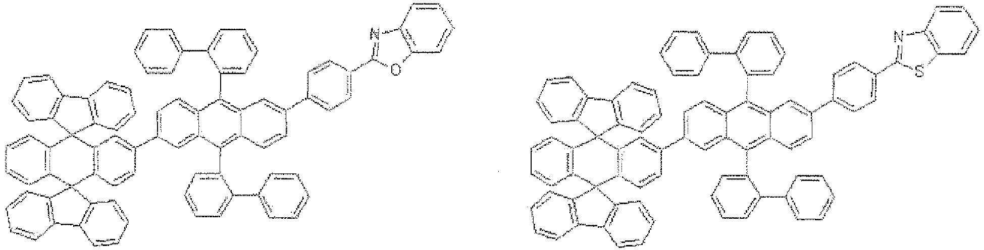


- When R7 and R8 are connected to each other to form one ring in
Formula 3, the compound may be represented by the followingFormula 5.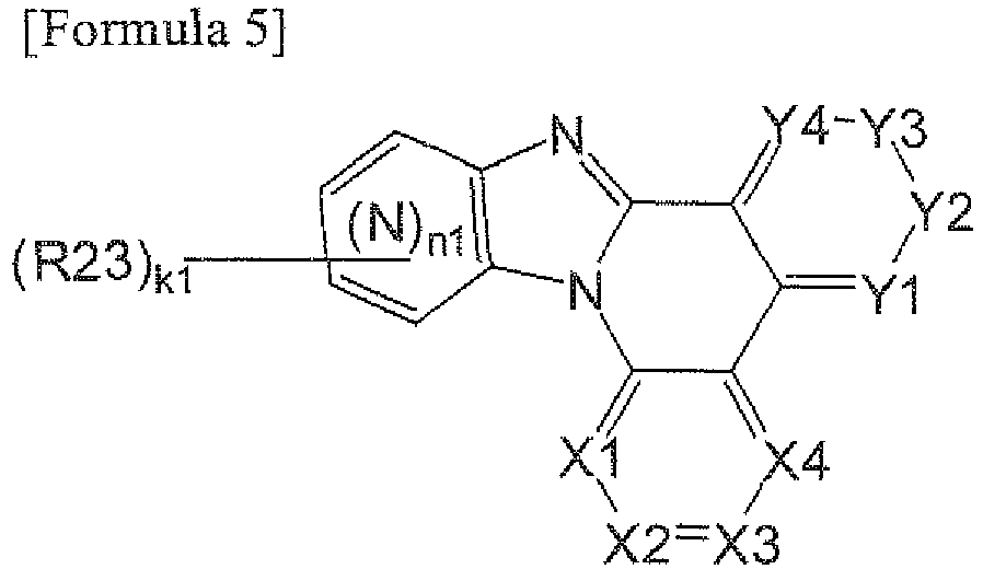
- In
Formula 5, X1 to X4 and Y1 to Y4 are the same as those defined inFormula 3,
N in (N)n1 means a nitrogen atom, and indicates that a nitrogen atom may replace a carbon atom in a benzene ring,
n1 in (N)n1 is an integer of 0 to 6, and
R23 is the same as R9 to R16 defined inFormula 3,
k1 is an integer of 0 to 4, and when k1 is an integer of 2 or higher, R11 may be different from each other. - When R7 and R8 are connected to each other to form a polycycling ring having two or more rings in
Formula 3, the compound may be represented by the followingFormulas 

- In
Formulas Formula 3,
N in (N)n1 and (N)n2 means a nitrogen atom, and indicates that a nitrogen atom may replace a carbon atom in a benzene ring,
n1 in (N)n1 is an integer of 0 to 2, and n2 in (N)n2 is an integer of 0 to 2,
R23 and R24 are the same as R9 to R16 defined inFormula 3,
inFormula 6, k1 is an integer of 0 to 4 and k2 is an integer of 0 to 4,
inFormula 7, k1 is an integer of 0 to 4 and k2 is an integer of 0 to 2, and
when k1 is an integer of 2 or higher, R23 may be different from each other, and when k2 is an integer of 2 or higher, R24 may be different from each other. - In
Formula 3, when R7 and R8 do not form a ring, R7 and R8 may be a phenyl group which is unsubstituted or substituted by R23 and R24, or a hexagonal heteroaromatic ring group that comprises a substituted or unsubstituted nitrogen (N) atom. For example,Formula 3 may be represented by the followingFormula 8.
- In
Formula 8, X1 to X4 and Y1 to Y4 are the same as those defined inFormula 3,
N in (N)n1 and (N)n2 means a nitrogen atom, and indicates that a nitrogen atom may replace a carbon atom in a benzene ring,
n1 in (N)n1 is an integer of 0 to 2, and n2 in (N)n2 is an integer of 0 to 2,
R23 and R24 are the same as R9 to R16 defined inFormula 3,
K1 is an integer of 0 to 4 and k2 is an integer of 0 to 4, and when k1 is an integer of 2 or higher, R23 may be different from each other, and when k2 is an integer of 2 or higher, R24 may be different from each other. - Specific examples of the compounds in
Formulas 


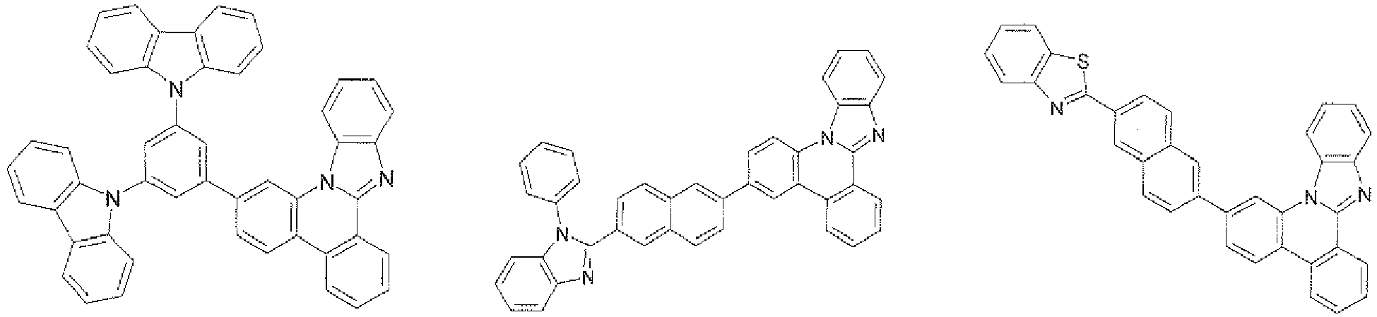


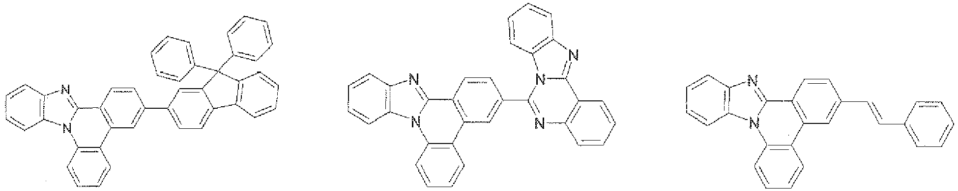





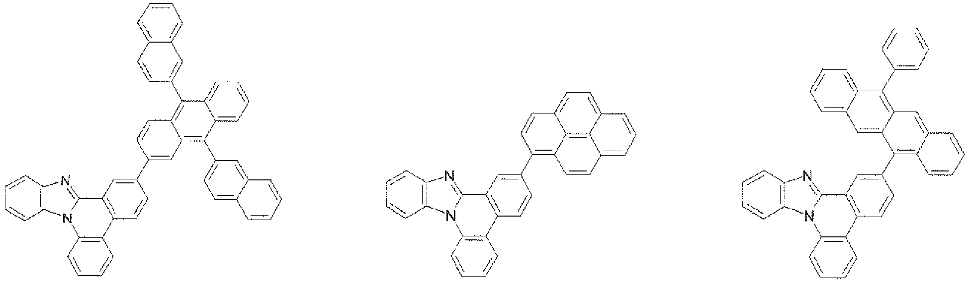


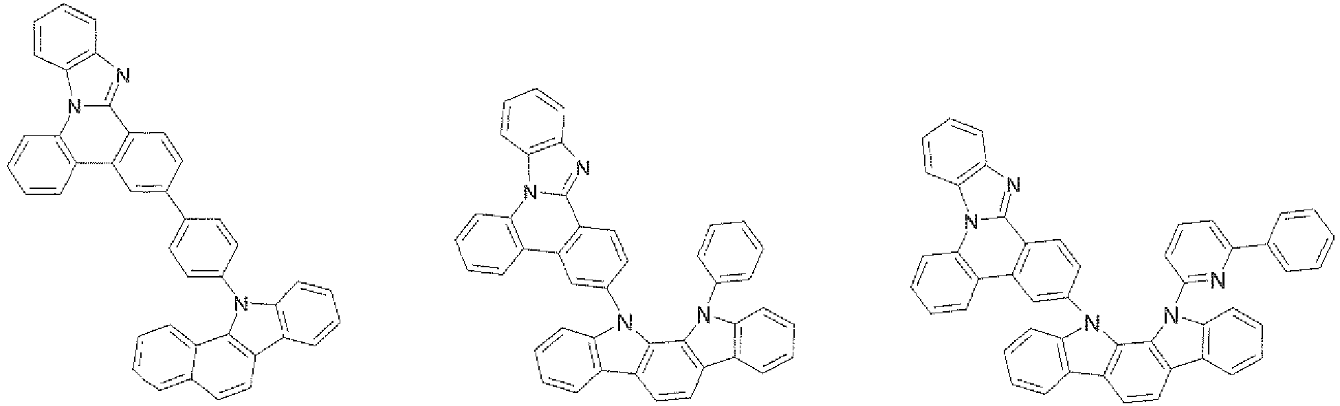

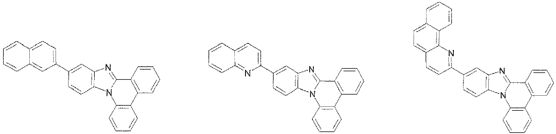


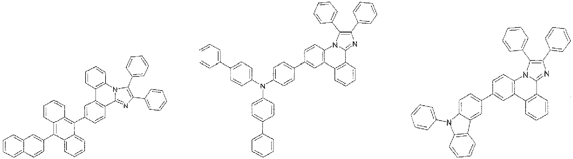


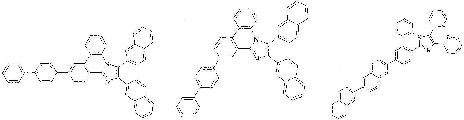





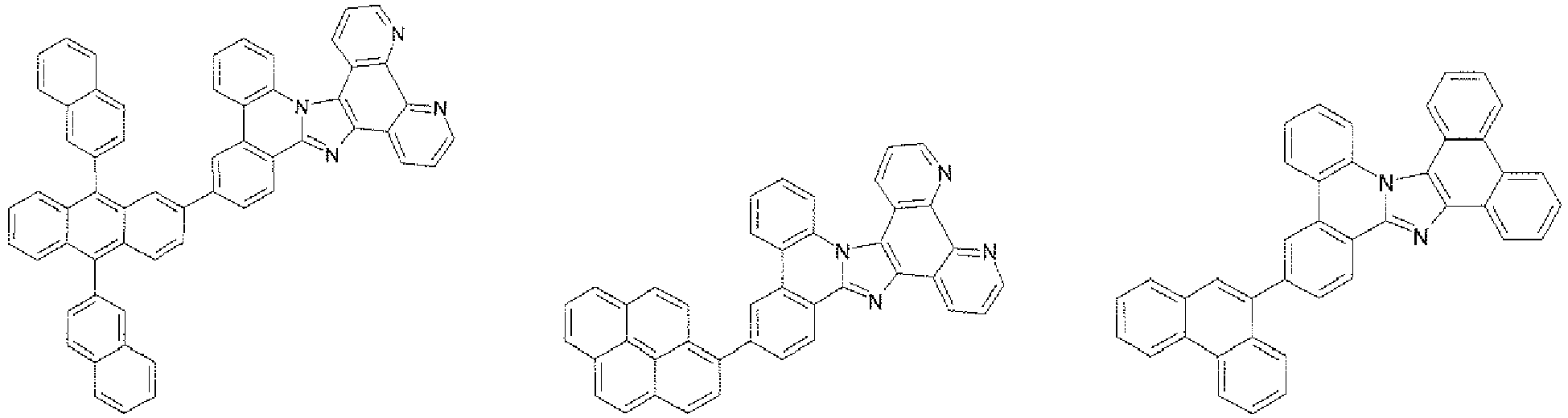


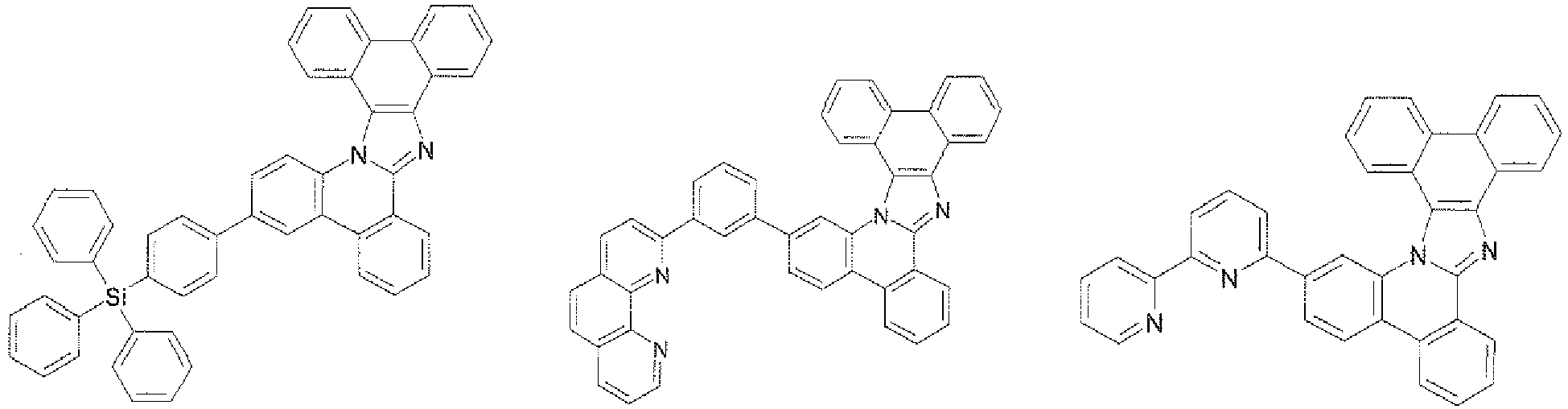


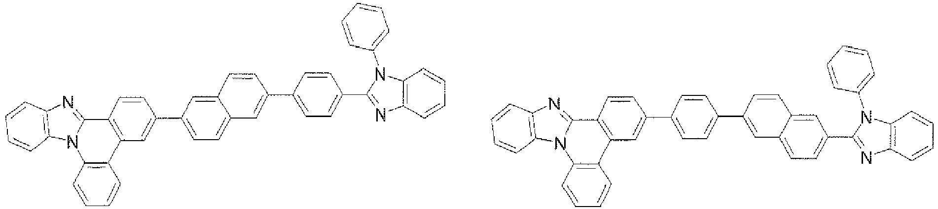





- The compound represented by
Formula 4 may be represented by one of the group consisting of the following structural formulas, but is not limited thereto.


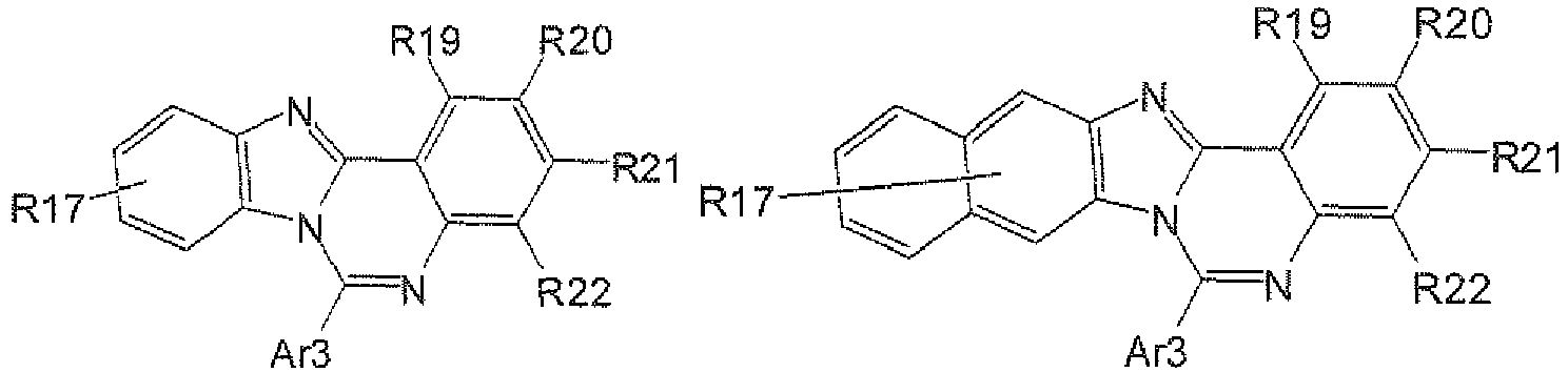
- In the structural formulas, R17 to R22 and Ar3 are the same as those defined in
Formula 4. - Further, the compound represented by
Formula 4 may be represented by the followingFormula 10, but is not limited thereto.
- In
Formula 10, Ar3 is selected from the following Table.


- In addition, the compound represented by
Formula 4 may be represented by one of the following structural formulas, but is not limited thereto.


- As shown in
FIG. 1 , an organic light emitting device typically consists of asubstrate 1, ananode 2, ahole injection layer 5, ahole transporting layer 6, alight emitting layer 7, anelectron transporting layer 8, and acathode 4, and actually each layer may be constituted by a plurality of layers, or two or more materials may be mixed to form a layer, and an electron injection layer may be inserted in order to facilitate the injection of electrons between theelectron transporting layer 8 and thecathode 4. - In the organic light emitting device structure as above, in order to transfer holes derived from the
anode 2 to thelight emitting layer 7, when a hole transporting material, which is disposed between theanode 2 and thelight emitting layer 7 and in contact with thelight emitting layer 7, is a material having a fluorescent light emitting efficiency which is equal to or greater than that of NPB, electric charges (holes and electrons) injected from theanode 2 and thecathode 4 fail to be converted into light in thelight emitting layer 7 and move toward a hole injection or transporting material layer which is in contact with the light emitting layer to contribute to light emission of the hole injection or transporting material, thereby deteriorating the characteristics of the device. - In order to determine whether a material was better than NPB in terms of fluorescent light emitting properties, films having a thickness of 100 nm or more were respectively formed on a glass substrate by using a material which is in contact with the light emitting layer and is disposed between the light emitting layer and the anode and NPB, and UV wavelengths of the same intensity were irradiated thereon to compare the PL spectrum. At this time, a material having an intensity which is equal to or greater than the PL spectrum intensity of NPB based on the Max. peak of the spectrum is defined as a material which is equivalent to or better than NPB in fluorescent light emitting properties.
- Materials are not particularly limited so long as they are equal to or better than NPB in fluorescent light emitting properties and have the above-mentioned properties as a material for forming a hole injection and transporting layer which is in contact with the light emitting layer, and any material typically used as an electric charge transporting material of holes in photoconductive materials in the related art may be used, or any one selected from known materials which are used in a hole injection layer of the EL device may be used. Further, in addition to the aromatic amine derivative layer and the nitrogen-containing heterocyclic derivative layer, a layer constituting the hole transporting region may be provided, and any material for forming these layers may be selected from known materials as described above and used.
- More specifically, examples of the compound having a fluorescent light emitting efficiency which is equal to or greater than that of NPB comprise compounds of the following
Formulas 11 to 16, and the like, but are not limited thereto.
- In
Formula 11, Ar16 to Ar27 are the same as or different from each other and are each independently a substituted or unsubstituted aryl group having 6 to 50 carbon atoms, or a substituted or unsubstituted heteroaryl group having 5 to 50 carbon atoms, and Ar22 and Ar23, Ar24 and Ar25, or Ar26 and Ar27 may be connected to each other to form a saturated or unsaturated cyclic group, and
a, b, c, p, q, and r are each independently an integer of 0 to 3, but at least one of a, b, and c is not 0.
- In
Formula 12, Ar28 to Ar31 are the same as or different from each other and are each independently a substituted or unsubstituted aryl group having 6 to 50 carbon atoms, or a substituted or unsubstituted heteroaryl group having 5 to 50 carbon atoms, and Ar29 and Ar30 may be connected to each other to form a saturated or unsaturated cyclic group,
L1 is a direct bond, a substituted or unsubstituted arylene group having 6 to 50 carbon atoms, or a substituted or unsubstituted heteroarylene group having 5 to 50 carbon atoms, and
x is an integer of 0 to 5.

- In
Formula 13, L2 is a substituted or unsubstituted arylene group having 10 to 40 carbon atoms, and
Ar32 to Ar35 are the same as or different from each other and are each independently a substituted or unsubstituted aryl group having 6 to 50 carbon atoms, or a substituted or unsubstituted heteroaryl group having 5 to 50 carbon atoms, and Ar32 and Ar33 or Ar34 and Ar35 may be connected to each other, or one of Ar32 to Ar35 may be connected to L2 or a substituent group of L2 to form a saturated or unsaturated cyclic group. - Specific examples of L2 in
Formula 13 comprise a biphenylene group, a terphenylene group, a quaterphenylene group, a naphthylene group, an anthracenylene group, a phenanthrylene group, a chrysenylene group, a pyrenylene group, a fluorenylene group, a 2,6-diphenylnaphthalene-4',4"-ene group, 2-phenylnaphthalene-2,4'-ene group, a 1-phenylnaphthalene-1,4'-ene group, a 2,7-diphenylfluorenylene-4'4"-ene group, a fluorenylene group, a 9,10-diphenylanthracenylene-4',4"-ene group, a 6,12-diphenylchrysenylen-4',4"-ene group and the like. - Preferable examples of L2 in
Formula 13 comprise a biphenylene group, a terphenylene group, a fluorenylene group, a 2-phenylnaphthalene-2,4'-ene group, a 1-phenylnaphthalene-1,4'-ene group, and a 6,12-diphenylchrysenylen-4',4"-ene group.


- In
Formulas
R1 to R12 are the same as or different from each other and are each independently selected from the group consisting of a hydrogen, a halogen, an alkyl group having 1 to 10 carbon atoms, an alkenyl group having 2 to 10 carbon atoms, an alkoxy group having 1 to 10 carbon atoms, an aryl group having 6 to 20 carbon atoms, and a heteroaryl group having 5 to 20 carbon atoms,
Ar1 and Ar2 are the same as or different from each other and are each independently selected from the group consisting of an aryl group having 6 to 20 carbon atoms and a heteroaryl group having 5 to 20 carbon atoms, and
m and n are each independently an integer of 0 to 4.

- In
Formula 16, X1 is an N-carbazolyl group which is unsubstituted or substituted by one or more selected from the group consisting of a halogen, an alkyl group having 1 to 10 carbon atoms, an alkoxy group having 1 to 10 carbon atoms, and an aryl group having 6 to 20 carbon atoms; an N-phenoxazyl group which is unsubstituted or substituted by one or more selected from the group consisting of a halogen, an alkyl group having 1 to 10 carbon atoms, an alkoxy group having 1 to 10 carbon atoms, and an aryl group having 6 to 20 carbon atoms; or an N-phenothiazyl group which is unsubstituted or substituted by one or more selected from the group consisting of a halogen, an alkyl group having 1 to 10 carbon atoms, an alkoxy group having 1 to 10 carbon atoms, and an aryl group having 6 to 20 carbon atoms,
X1 is an N-carbazolyl group which is unsubstituted or substituted by one or more selected from the group consisting of a halogen, an alkyl group having 1 to 10 carbon atoms, an alkoxy group having 1 to 10 carbon atoms, and an aryl group having 6 to 20 carbon atoms; an N-phenoxazyl group which is unsubstituted or substituted by one or more selected from the group consisting of a halogen, an alkyl group having 1 to 10 carbon atoms, an alkoxy group having I to 10 carbon atoms, and an aryl group having 6 to 20 carbon atoms; or an N-phenothiazyl group which is unsubstituted or substituted by one or more selected from the group consisting of a halogen, an alkyl group having 1 to 10 carbon atoms, an alkoxy group having 1 to 10 carbon atoms, and an aryl group having 6 to 20 carbon atoms,
X2 is an N-carbazolyl group which is unsubstituted or substituted by one or more selected from the group consisting of a halogen, an alkyl group having 1 to 10 carbon atoms, an alkoxy group having 1 to 10 carbon atoms, and an aryl group having 6 to 20 carbon atoms; an N-phenoxazyl group which is unsubstituted or substituted by one or more selected from the group consisting of a halogen, an alkyl group having 1 to 10 carbon atoms, an alkoxy group having I to 10 carbon atoms, and an aryl group having 6 to 20 carbon atoms; an N-phenothiazyl group which is unsubstituted or substituted by one or more selected from the group consisting of a halogen, an alkyl group having 1 to 10 carbon atoms, an alkoxy group having 1 to 10 carbon atoms, and an aryl group having 6 to 20 carbon atoms; or -NAr1Ar2, and
Ar1 and Ar2 are each independently an aryl group having 6 to 20 carbon atoms, which is unsubstituted or substituted by one or more selected from the group consisting of a halogen, an alkyl group, an alkoxy group, and an aryl group; or a heteroaryl group having 5 to 20 carbon atoms, which is unsubstituted or substituted by one or more selected from the group consisting of a halogen, an alkyl group, an alkoxy group, and an aryl group,
B1 and B2 are the same as or different from each other and are each independently a hydrogen; a deuterium; an alkyl group; an aryl group having 6 to 20 carbon atoms, which is unsubstituted or substituted by one or more selected from the group consisting of a halogen, an alkyl group, an alkoxy group, and an aryl group; a heteroaryl group having 5 to 20 carbon atoms, which is unsubstituted or substituted by one or more selected from the group consisting of a halogen, an alkyl group, an alkoxy group, and an aryl group; or an aralkyl group which is unsubstituted or substituted by one or more selected from the group consisting of a halogen, an alkyl group, an alkoxy group, and an aryl group, and
Z1 and Z2 are the same as or different from each other and are each independently a hydrogen; a deuterium; a halogen; an alkyl group; an alkoxy group; an aryl group having 6 to 20 carbon atoms, which is selected from the group consisting of a halogen, an alkyl group, an alkoxy group, and an aryl group; or a heteroaryl group having 5 to 20 carbon atoms, which is selected from the group consisting of a halogen, an alkyl group, an alkoxy group, and an aryl group. - The compound represented by
Formula 13 may be represented by the followingFormula 17.
- In
Formula 17, Ar32 to Ar35 are the same as those defined inFormula 13,
Ra each independently represents a hydrogen, a deuterium, a halogen, an alkyl group, an aralkyl group, an alkenyl group, a cyano group, an amino group, an acyl group, an alkoxycarbonyl group, a carboxyl group, an alkoxy group, an aryloxy group, an alkylsulfonyl group, a hydroxyl group, an amide group, an aryl group, or a heteroaryl group, and these may be additionally substituted and may form a ring with those which are adjacent to each other, and
n represents an integer of 2 to 4. - In
Formula 17, each of Ar32 to Ar35 may be connected to an adjacent aryl group connected to N or may be connected to Ra to form a substituted or unsubstituted ring. - The compound represented by
Formula 13 may be represented by the followingFormula 


- In
Formulas Formula 13, and
R23 to R27 are the same as or different from each other and each independently represent a hydrogen, a deuterium, a halogen, an alkyl group, an aralkyl group, an alkenyl group, a cyano group, an amino group, an acyl group, an alkoxycarbonyl group, a carboxyl group, an alkoxy group, an aryloxy group, an alkylsulfonyl group, a hydroxyl group, an amide group, an aryl group, or a heteroaryl group, and these may be additionally substituted and may form a ring with those which are adjacent to each other. - Further, at least one of Ar36 to Ar39 in
Formula 18 and at least one of Ar40 to Ar43 inFormula 19 are preferably a substituted or unsubstituted biphenyl group. Specific examples of the substituted or unsubstituted biphenyl group comprise a 2-biphenyl group, a 3-biphenyl group, a 4-biphenyl group, a p-terphenyl group, a m-terphenyl group, an o-terphenyl group, a 4'-methyl-biphenyl-4-yl group, a 4'-t-butyl-biphenyl-4-yl group, a 4'-(1-naphthyl)-biphenyl-4-yl group, a 4'-(2-naphthyl)-biphenyl-4-yl group, a 2-fluorenyl group, a 9,9-dimethyl-2-fluorenyl group, and the like. Preferably, the examples comprise a 3-biphenyl group, a 4-biphenyl group, a p-terphenyl group, a m-terphenyl group, and a 9,9-dimethyl-2-fluorenyl group. At the terminal of the substituted or unsubstituted biphenyl group, an arylamino group may be substituted. - Specific examples of the compound in
Formula 13 comprise the following structural formulas, and the like, but are not limited thereto.


- R1 to R12 in
Formulas Formulas - In the N-carbazolyl group in
Formulas 
- R1 to R8 in
Formulas - Specific examples of the compounds in
Formulas 


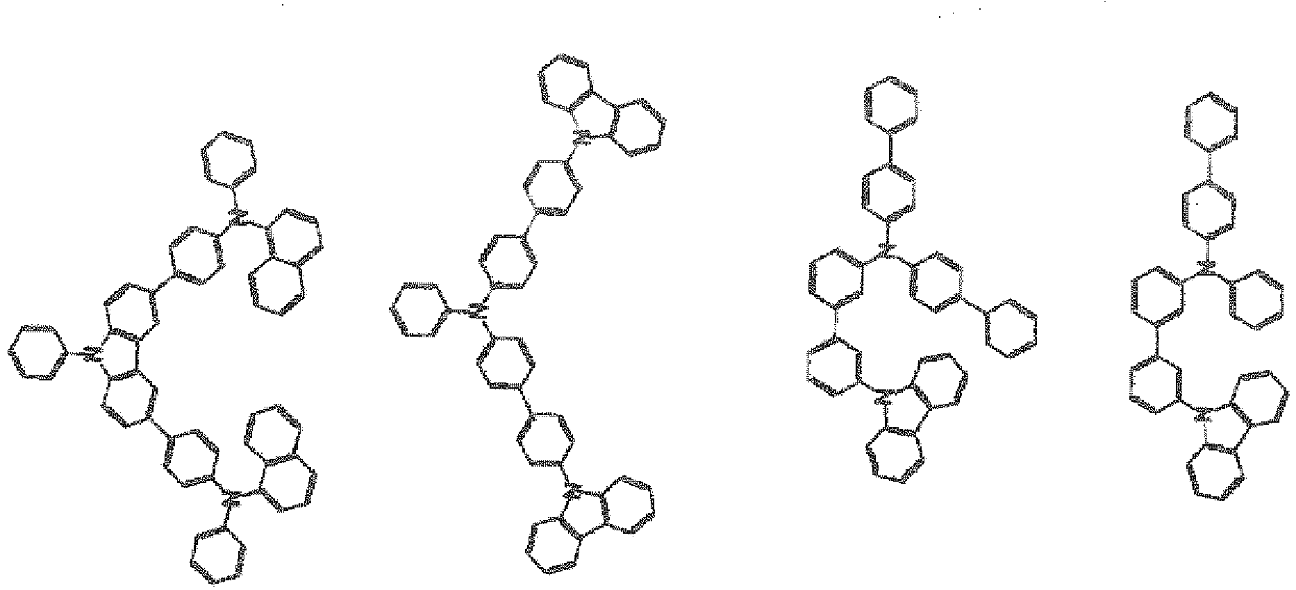

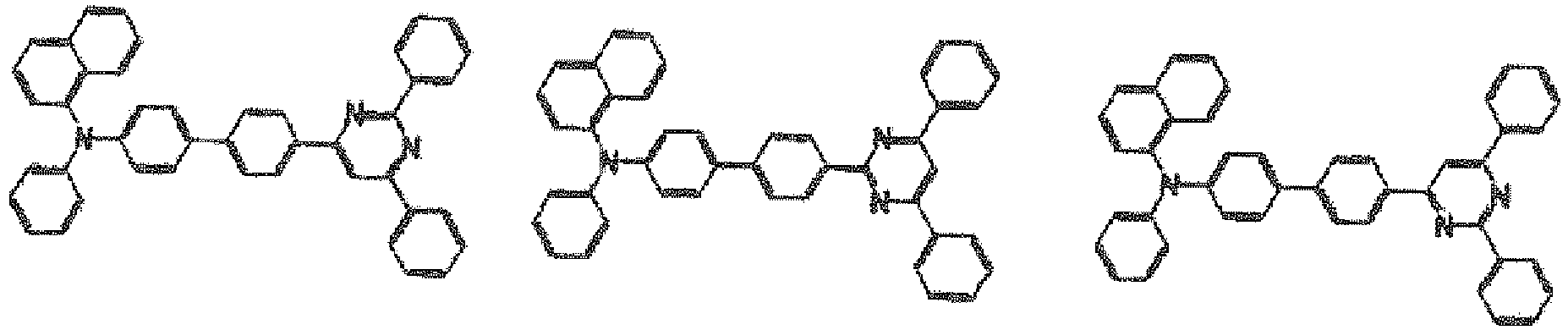


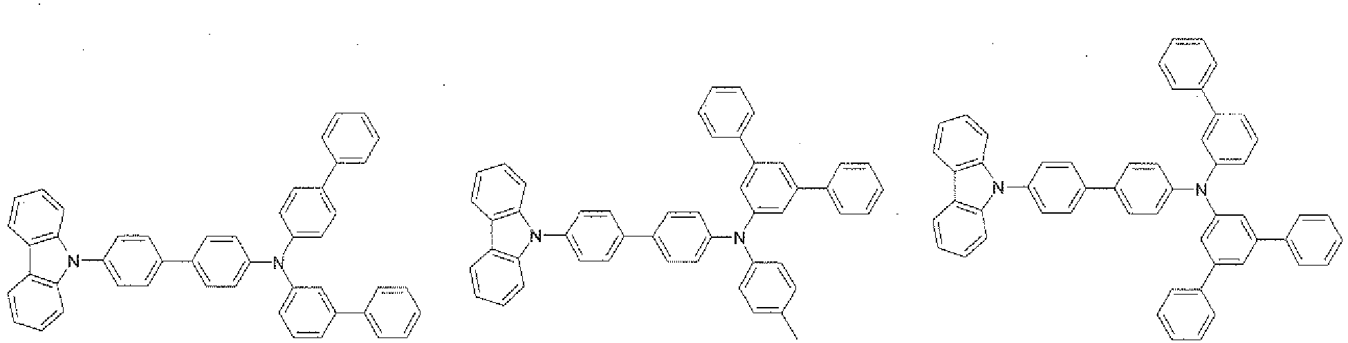

- Specific examples of the substituted or unsubstituted N-carbazolyl group, substituted or unsubstituted N-phenoxazyl group, or substituted or unsubstituted N-phenothiazyl group of X1 in Formula 16 comprise an N-carbazolyl group, a 2-methyl-N-carbazolyl group, a 3-methyl-N-carbazolyl group, a 4-methyl-N-carbazolyl group, a 3-n-butyl-N-carbazolyl group, a 3-n-hexyl-N-carbazolyl group, a-3-n-octyl-N-carbazolyl group, a 3-n-decyl-N-carbazolyl group, a 3,6-dimethyl-N-carbazolyl group, a 2-methoxy-N-carbazolyl group, a 3-methoxy-N-carbazolyl group, a 3-ethoxy-N-carbazolyl group, a 3-isopropoxy-N-carbazolyl group, a 3-n-butoxy-N-carbazolyl group, a 3-n-octyloxy-N-carbazolyl group, a 3-n-decyloxy-N-carbazolyl group, a 3-phenyl-N-carbazolyl group, a 3-(4'-methylphenyl)-N-carbazolyl group, a 3-chloro-N-carbazolyl group, an N-phenoxazyl group, an N-phenothiazyl group, a 2-methyl-N-phenothiazyl group, and the like.
- Specific examples of the substituted or unsubstituted N-carbazolyl group, substituted or unsubstituted N-phenoxazyl group, and substituted or unsubstituted N-phenothiazyl group of X2 in
Formula 16 comprise a substituted or unsubstituted N-carbazolyl group, a substituted or unsubstituted N-phenoxazyl group, a substituted or unsubstituted N-phenothiazyl group which are exemplified as specific examples of X1, and the like. - In the -NAr1Ar2 in
Formula 16, Ar1 and Ar2 represent a substituted or unsubstituted aryl group or heteroaryl group. Specific examples of the Ar1 and Ar2 comprise a phenyl group, a 1-naphthyl group, a 2-naphthyl group, a 2-anthryl group, a 9-anthryl group, a 4-quinolyl group, a 4-pyridyl group, a 3-pyridyl group, a 2-pyridyl group, a 3-furyl group, a 2-furyl group, a 3-thienyl group, a 2-thienyl group, a 2-oxazolyl group, a 2-thiazolyl group, a 2-benzoxazolyl group, a 2-benzothiazolyl group, a 2-benzoimidazolyl group, a 4-methylphenyl group, a 3-methylphenyl group, a 2-methylphenyl group, a 4-ethylphenyl group, a 3-ethylphenyl group, a 2-ethylphenyl group, a 4-n-propylphenyl group, a 4-isopropylphenyl group, a 2-isopropylphenyl group, a 4-n-butylphenyl group, a 4-isobutylphenyl group, a 4-sec-butylphenyl group, a 2-sec-butylphenyl group, a 4-tert-butylphenyl group, a 3-tert-butylphenyl group, a 2-tert-butylphenyl group, a 4-n-pentylphenyl group, a 4-isopentylphenyl group, a 2-neopentylphenyl group, a 4-tert-pentylphenyl group, a 4-n-hexylphenyl group, a 4-(2'-ethylbutyl)phenyl group, a 4-n-heptylphenyl group, a 4-n-octylphenyl group, a 4-(2'-ethylhexyl)phenyl group, a 4-tert-octylphenyl group, a 4-n-decylphenyl group, a 4-n-dodecylphenyl group, a 4-n-tetradecylphenyl group, a 4-cyclopentylphenyl group, a 4-cyclohexylphenyl group, a 4-(4'-methylcyclohexyl)phenyl group, a 4-(4'-tert-butylcyclohexyl)phenyl group, a 3-cyclohexylphenyl group, a 2-cyclohexylphenyl group, a 4-ethyl-1-naphthyl group, a 6-n-butyl-2-naphthyl group, a 2,4-dimethylphenyl group, a 2,5-dimethylphenyl group, a 3,4-dimethylphenyl group, a 3,5-dimethylphenyl group, a 2,6-dimethylpbenyl group, a 2,4-diethylphenyl group, a 2,3,5-trimethylphenyl group, a 2,3,6-trimethylphenyl group, a 3,4,5-trimethylphenyl group, a 2,6-diethylphenyl group, a 2,5-diisopropylphenyl group, a 2,6-diisobutylphenyl group, a 2,4-di-tert-butylphenyl group, a 2,5-di-tert-butylphenyl group, a 4,6-di-tert-butyl-2-methylphenyl group, a 5-tert-butyl-2-methylphenyl group, a 4-tert-butyl-2,6-dimethylphenyl group, a 4-methoxyphenyl group, a 3-methoxyphenyl group, a 2-methoxyphenyl group, a 4-ethoxyphenyl group, a 3-ethoxyphenyl group, a 2-ethoxyphenyl group, a 4-n-propoxyphenyl group, a 3-n-propoxyphenyl group, a 4-isopropoxyphenyl group, a 2-isopropoxyphenyl group, a 4-n-butoxyphenyl group, a 4-isobutoxyphenyl group, a 2-see-butoxyphenyl group, a 4-n-pentyloxyphenyl group, a 4-isopentyloxyphenyl group, a 2-isopentyloxyphenyl group, a 4-neopentyloxyphenyl group, a 2-neopentyloxyphenyl group, a 4-n-hexyloxyphenyl group, a 2-(2'-ethylbutyl)oxyphenyl group, 4-n-octyloxyphenyl group, a 4-n-decyloxyphenyl group, a 4-n-dodecyloxyphenyl group, a 4-n-tetradecyloxyphenyl group, a 4-cyclohexyloxyphenyl group, a 2-cyclohexyloxyphenyl group, a 2-methoxy-1-naphthyl group, a 4-methoxy-1-naphthyl group, a 4-n-butoxy-1-naphthyl group, a 5-ethoxy-1-naphthyl group, a 6-methoxy-2-naphthyl group, a 6-ethoxy-2-naphthyl group, a 6-n-butoxy-2-naphthyl group, a 6-n-hexyloxy-2-naphthyl group, a 7-methoxy-2-naphthyl group, a 7-n-butoxy-2-naphthyl group, a 2-methyl-4-methoxyphenyl group, a 2-methyl-5-methoxyphenyl group, a 3-methyl-5-methoxyphenyl group, a 3-ethyl-5-methoxyphenyl group, a 2-methoxy-4-methylphenyl group, a 3-methoxy-4-methylphenyl group, a 2,4-dimethoxyphenyl group, a 2,5-dimethoxyphenyl group, a 2,6-dimethoxyphenyl group, a 3,4-dimethoxyphenyl group, a 3,5-dimethoxyphenyl group, a 3,5-diethoxyphenyl group, a 3,5-di-n-butoxyphenyl group, a 2-methoxy-4-ethoxyphenyl group, a 2-methoxy-6-ethoxyphenyl group, a 3,4,5-trimethoxyphenyl group, a 4-phenylphenyl group, a 3-phenylphenyl group, a 2-phenylphenyl group, a 4-(4'-methylphenyl)phenyl group, a 4-(3'-methylphenyl)phenyl group, a 4-(4'-methoxyphenyl)phenyl group, a 4-(4'-n-butoxyphenyl)phenyl group, a 2-(2'-methoxyphenyl)phenyl group, a 4-(4'-chlorophenyl)phenyl group, a 3-methyl-4-phenylphenyl group, a 3-methoxy-4-phenylphenyl group, a 4-fluorophenyl group, a 3-fluorophenyl group, a 2-fluorophenyl group, a 4-chlorophenyl group, a 3-chlorophenyl group, a 2-chlorophenyl group, a 4-bromophenyl group, a 2-bromophenyl group, a 4-chloro-1-naphthyl group, a 4-chloro-2-naphthyl group, a 6-bromo-2-naphthyl group, a 2,3-difluorophenyl group, a 2,4-difluorophenyl group, a 2,5-difluorophenyl group, a 2,6-difluorophenyl group, a 3,4-dilfuorophenyl group, a 3,5-difluorophenyl group, a 2,3-dichlorophenyl group, a 2,4-dichlorophenyl group, a 2,5-dichlorophenyl group, a 3,4-dichlorophenyl group, a 3,5-dichlorophenyl group, a 2,5-dibromophenyl group, a 2,4,6-trichlorophenyl group, a 2,4-dichloro-1-naphthyl group, a 1,6-dichloro-2-naphthyl group, a 2-fluoro-4-methylphenyl group, a 2-fluoro-5-methylphenyl group, a 3-fluoro-2-methylphenyl group, a 3-fluoro-4-methylphenyl group, a 2-methyl-4-fluorophenyl group, a 2-methyl-5-fluorophenyl group, a 3-methyl-4-fluorophenyl group, a 2-chloro-4-methylphenyl group, a 2-chloro-5-methylphenyl group, a 2-chloro-6-methylphenyl group, a 2-methyl-3-chlorophenyl group, a 2-methyl-4-chlorophenyl group, a 3-methyl-4-chlorophenyl group, a 2-chloro-4,6-dimethylphenyl group, a 2-methoxy-4-fluorophenyl group, a 2-fluoro-4-methoxyphenyl group, a 2-fluoro-4-ethoxyphenyl group, a 2-fluoro-6-methoxyphenyl group, a 3-fluoro-4-ethoxyphenyl group, a 3-chloro-4-methoxyphenyl group, a 2-methoxy-5-chlorophenyl group, a 3-methoxy-6-chlorophenyl group, a 5-chloro-2,4-dimethoxyphenyl group, and the like, but are not limited thereto. - Specific examples of the compound represented by
Formula 16 comprise the following compounds (Nos. 1 to 100), but the present invention is not limited thereto. - 1. 7-(N'-carbazolyl)-N,N-diphenyl-9H-fluorene-2-amine
- 2. 7-(N'-carbazolyl)-N-phenyl-N-(4'-methylphenyl)-9-methyl-9H-fluorene-2-amine
- 3. 7-(N'-carbazolyl)-N,N-diphenyl-9,9-diphenyl-9H-fluorene-2-amine
- 4. 7-(N'-carbazolyl)-N-phenyl-N-(3'-methylphenyl)-9,9-dimethyl-9H-fluorene-2-amine
- 5. 7-(N'-carbazolyl)-N-phenyl-N-(4'-methylphenyl)-9,9-dimethyl-9H-fluorene-2-amine
- 6. 7-(N'-carbazolyl)-N-phenyl-N-(4'-ethylphenyl)-9.9-dimethyl-9H-fluorene-2-amine
- 7. 7-(N'-carbazolyl)-N-phenyl-N-(4'-tert-butylphenyl)-9,9-dimethyl-9H-fluorene-2-amine
- 8. 7-(N'-carbazolyl)-N-phenyl-N-(3',4'-dimethyphenyl)-9,9-dimethyl-9H-fluorene-2-amine
- 9. 7-(N'-carbazolyl)-N-phenyl-N-(3',5'-dimethylphenyl)-9,9-dimethyl-9H-fluorene-2-amine
- 10. 7-(N'-carbazolyl)-N,N-di(3'-methylphenyl)-[0410]9,9-dimethyl-9H-fluorene-2-amine
- 11. 7-(N'-carbazolyl)-N,N-di(4'-methylphenyl)-9,9-dimethyl-9H-fluorene-2-amine
- 12. 7-(N'-carbazolyl)-N,N-di(4'-ethylphenyl)-9,9-dimethyl-9H-fluorene-2-amine
- 13. 7-(N'-carbazolyl)-N-phenyl-N-(3'-methoxyphenyl)-9,9-dimethyl-9H-fluorene-2-amine
- 14. 7-(N'-carbazolyl)-N-phenyl-N-(4'-methoxyphenyl)-9,9-dimethyl-9H-fluorene-2-amine
- 15. 7-(N'-carbazolyl)-N-phenyl-N-(4'-ethoxyphenyl)-9,9-dimethyl-9H-fluorene-2-amine
- 16. 7-(N'-carbazolyl)-N-phenyl-N-(4'-n-buthoxyphenyl)-9,9-dimethyl-9H-fluorene-2-amine
- 17. 7-(N'-carbazolyl)-N,N-di(4'-methoxyphenyl)-9,9-dimethyl-9H-fluorene-2-amine
- 18. 7-(N'-carbazolyl)-N-(3'-methylphenyl)-N-(4"-methoxyphenyl)-9,9-dimethyl-9H-fluorene-2-amine
- 19. 7-(N'-carbazolyl)-N-(4'-methylphenyl)-N-(4"-methoxyphenyl)-9,9-dimethyl-9H-fluorene-2-amine
- 20. 7-(N'-carbazolyl)-N-phenyl-N-(3'-fluorophenyl)-9,9-dimethyl-9H-fluorene-2-amine
- 21. 7-(N'-carbazolyl)-N-phenyl-N-(4'-chlorophenyl)-9,9-dimethyl-9H-fluorene-2-amine
- 22. 7-(N'-carbazolyl)-N-phenyl-N-(4'-phenylphenyl)-9,9-dimethyl-9H-fluorene-2-amine
- 23. 7-(N'-carbazolyl)-N-phenyl-N-(1'-naphthyl)-9,9-dimethyl-9H-fluorene-2-amine
- 24. 7-(N'-carbazolyl)-N-phenyl-N-(2'-naphthyl)-9,9-dimethyl-9H-fluorene-2-amine
- 25. 7-(N'-carbazolyl)-N-(4'-methylphenyl)-N-(2"-naphthyl-9,9-dimethyl-9H-fluorene-2-amine
- 26. 7-(N'-carbazolyl)-N-phenyl-N-(2'-furyl)-9,9-dimethyl-9H-fluorene-2-amine
- 27. 7-(N'-carbazolyl)-N-phenyl-N-(2'-thienyl)-9,9-dimethyl-9H-fluorene-2-amine
- 28. 7-(N'-carbazolyl)-N,N-diphenyl-4-fluoro-9,9-dimethyl-9H-fluorene-2-amine
- 29. 7-(N'-carbazolyl)-N,N-diphenyl-3-methoxy-9,9-dimethyl-9H-fluorene-2-amine
- 30. 7-(N'-carbazolyl)-N,N-diphenyl-4-phenyl-9,9-dimethyl-9H-fluorene-amine
- 31. 7-(3'-methyl-N'-carbazolyl)-N,N-diphenyl-9,9-dimethyl-9H-fluorene-2-amine
- 32. 7-(3'-methoxy-N'-carbazolyl)-N,N-diphenyl-9,9-dimethyl-9H-fluorene-2-amine
- 33. 7-(3'-chloro-N'-carbazolyl)-N,N-diphenyl-9,9-dimethyl-9H-fluorene-2-amine
- 34. 2,7-di(N-carbazolyl)-9,9-dimethyl-9H-fluorene
- 35. 7-(N'-phenoxazyl)-N,N-diphenyl-9,9-dimethyl-9H-fluorene-2-amine
- 36. 7-(N'-phenoxazyl)-N,N-di(4'-methylphenyl)-9,9-dimethyl-9H-fluorene-2-amine
- 37. 2,7-di(N-phenoxazyl)-9,9-dimethyl-9H-fluorene
- 38. 7-(N'-phenothiazyl)-N,N-diphenyl-9,9-dimethyl-9H-fluorene-2-amine
- 39. 7-(N'-phenothiazyl)-N-phenyl-N-(3'-methylphenyl)-9,9-dimethyl-9H-fluorene-2-amine
- 40. 7-(N'-phenothiazyl)-N-phenyl-N-(4'-methylphenyl)-9,9-dimethyl-9H-fluorene-2-amine
- 41. 7-(N'-phenothiazyl)-N,N-di(4'-methylphenyl)-9,9-dimethyl-9H-fluorene-2-amine
- 42. 7-(N'-phenothiazyl)-N-phenyl-N-(4'-methoxyphenyl)-9,9-dimethyl-9H-fluorene-2-amine
- 43. 7-(N'-phenothiazyl)-N-phenyl-N-(2'-naphthyl)-9,9-dimethyl-9H-fluorene-2-amine
- 44. 2,7-di(N-phenothiazyl)-9,9-dimethyl-9,9-dimethyl-9H-fluorene
- 45. 7-(N'-carbazolyl)-N,N-diphenyl-9,9-diethyl-9H-fluorene-2-amine
- 46. 7-(N'-carbazolyl)-N-phenyl-N-(4'-methylphenyl)-[0446] 9,9-diethyl-9H-fluorene-2-amine
- 47. 7-(N'-carbazolyl)-N,N-di(4'-methylphenyl)-9,9-diethyl-9H-fluorene-2-amine
- 48. 7-(N'-carbazolyl)-N-phenyl-N-(3'-methoxyphenyl)-9,9-diethyl-9H-fluorene-2-amine
- 49. 7-(N'-carbazolyl)-N,N-diphenyl-4-methyl-9,9-diethyl-9H-fluorene-2-amine
- 50. 7-(N'-carbozolyl)-N,N-diphenyl-9-isopropyl-9H-fluorene-2-amine
- 51. 7-(N'-carbazolyl)-N,N-diphenyl-9,9-di-n-propyl-9H-fluorene-2-amine
- 52. 7-(N'-carbazolyl)-N-phenyl-N-(4'-methylphenyl)-9,9-di-n-propyl-9H-fluorene-2-amine
- 53. 7-(N'-carbazolyl)-N-phenyl-N-(4'-methoxyphenyl)-9,9-di-n-propyl-9H-fluorene-2-amine
- 54. 2,7-di(N-carbazolyl)-9,9-di-n-propyl-9H-fluorene
- 55. 2,7-di(N-phenoxazyl)-9,9-di-n-propyl-9H-fluorene
- 56. 7-(N'-carbazolyl)-N,N-diphenyl-9,9-di-n-butyl-9H-fluorene-2-amine
- 57. 7-(N'-carbazolyl)-N,N-di(4'-methylphenyl)-9,9-di-n-butyl-9H-fluorene-2-amine
- 58. 2,7-di(N'-carbazolyl)-9,9-di-n-butyl-9H-fluorene
- 59. 7-(N'-carbazolyl)-N-phenyl-N-(4'-methoxyphenyl)-9,9-di-n-pentyl-9H-fluorene-2-amine
- 60. 7-(N'-phenoxazyl)-N-phenyl-N-(3'-methoxyphenyl)-9,9-di-n-pentyl-9H-fluorene-2-amine
- 61. 7-(N'-carbazolyl)-N,N-di(4"-methoxyphenyl)-9,9-di-n-pentyl-9H-fluorene-2-amine
- 62. 2,7-di(N'-carbazolyl)-9,9-di-n-pentyl-9H-fluorene
- 63. 7-(N'-carbazolyl)-N,N-diphenyl-9,9-di-n-hexyl-9H-fluorene-2-amine
- 64. 7-(N'-carbazolyl)-N,N-di(4'-methylphenyl)-9,9-di-n-hexyl-9H-fluorene-2-amine
- 65. 7-(N'-carbazolyl)-N,N-diphenyl-9-cyclohexyl-9H-fluorene-2-amine
- 66. 7-(N'-carbazolyl)-N,N-diphenyl-9,9-di-n-octyl-9H-fluorene-2-amine
- 67. 7-(N'-phenoxazyl)-N,N-di(4'-methylphenyl)-9,9-di-n-octyl-9H-fluorene-2-amine
- 68. 7-(N'-carbazolyl)-N,N-diphenyl-9-methyl-9-ethyl-9H-fluorene-2-amine
- 69. 7-(N'-carbazolyl)-N,N-diphenyl-9-methyl-9-n-propyl-9H-fluorene-2-amine
- 70. 7-(N'-phenothiazyl)-N,N-diphenyl-9-methyl-9-n-propyl-9H-fluorene-2-amine
- 71. 7-(N'-carbazolyl)-N,N-diphenyl-9-ethyl-9-n-hexyl-9H-fluorene-2-amine
- 72. 7-(N'-carbazolyl)-N,N-diphenyl-9-ethyl-9-cyclohexyl-9H-fluorene-2-amine
- 73. 7-(N'-carbazolyl)-N,N-diphenyl-9-benzyl-9H-fluorene-2-amine
- 74. 7-(N'-carbazolyl)-N,N-diphenyl-9,9-dibenzyl-9H-fluorene-2-amine
- 75. 7-(N'-carbazolyl)-N,N-diphenyl-9,9-di(4'-methylbenzyl)-9H-fluorene-2-amine
- 76. 7-(N'-carbazolyl)-N,N-diphenyl-9,9-di(4'-methoxybenzyl)-9H-fluorene-2-amine
- 77. 7-(N'-carbazolyl)-N-phenyl-N-(4'-methylphenyl)-9,9-dibenzyl-9H-fluorene-2-amine
- 78. 7-(N'-carbazolyl)-N,N-di(4'-methylphenyl)-9,9-dibenzyl-9H-fluorene-2-amine
- 79. 7-(N'-carbazolyl)-N-phenyl-N-(4'-methoxyphenyl)-9,9-dibenzyl-9H-fluorene-2-amine
- 80. 7-(N'-carbazolyl)-N-phenyl-N-(4'-phenylphenyl)-9,9-dibenzyl-9H-fluorene-2-amine
- 81. 7-(N'-carbazolyl)-N-phenyl-N-(2'-naphthyl)-9,9-dibenzyl-9H-fluorene-2-amine
- 82. 7-(N'-phenoxazyl)-N-phenyl-N-(4'-methylphenyl)-[0482] 9,9-dibenzyl-9H-fluorene-2-amine
- 83. 7-(N'-phenothiazyl)-N,N-di(4'-methylphenyl)-9,9-dibenzyl-9H-fluorene-2-amine
- 84. 2,7-di(N-carbazolyl)-9,9-dibenzyl-9H-fluorene
- 85. 2,7-di(N-carbazolyl)-9,9-di(4'-methylbenzyl)-9H-fluorene
- 86. 2-(N-carbazolyl)-7-(N'-phenothiazyl)-9,9-dibenzyl-9H-fluorene
- 87. 7-(N'-carbazolyl)-N,N-diphenyl-9-methyl-9-benzyl-9H-fluorene-2-amine
- 88. 7-(N'-phenoxazyl)-N,N-diphenyl-9-ethyl-9-benzyl-9H-fluorene-2-amine
- 89. 7-(N'-carbazolyl)-N,N-diphenyl-9,9-diphenyl-9H-fluorene-2-amine
- 90. 7-(N'-carbazolyl)-N-phenyl-N-(4'-methylphenyl)-9,9-diphenyl-9H-fluorene-2-amine
- 91. 7-(N'-carbazolyl)-N,N-di(4'-methylphenyl)-9,9-diphenyl-9H-fluorene-2-amine
- 92. 7-(N'-carbazolyl)-N-phenyl-N-(3'-methylphenyl)-9,9-di(4"-methylphenyl)-9H-fluorene-2-amine
- 93. 7-(N'-carbazolyl)-N-phenyl-N-(3'-methylphenyl)-9,9-di(4"-methoxyphenyl)-9H-fluorene-2-amine
- 94. 7-(N'-phenoxazyl)-N,N-di(4'-methylphenyl)-9,9-diphenyl-9H-fluorene-2-amine
- 95. 7-(N'-phenothiazyl)-N,N-diphenyl-9,9-diphenyl-9H-fluorene-2-amine
- 96. 2.7-di(N'-carbazolyl)-9,9-di(4'-methylphenyl)-9H-fluorene
- 97. 2-(N-carbazolyl)-7-(N'-phenoxazyl)-9,9-diphenyl-9H-fluorene
- 98. 2-(N-phenoxazyl)-7-(N'-phenothiazyl)-9,9-diphenyl-9H-fluorene
- 99. 7-(N'-carbazolyl)-N-phenyl-N-(4'-methylphenyl)-9-methyl-9-phenyl-9H-fluorene-2-amine
- 100. 7-(N'-carbazolyl)-N,N-diphenyl-9-ethyl-9-phenyl-9H-fluorene-2-amine
- As the materials for the hole-injection layer and hole transporting layer, the above-mentioned substances may be used. However, porphyrin compounds (disclosed in Japanese Patent Application Laid-Open No.
Sho 63-295695 U.S. Pat. No. 4,127,412 , Japanese Patent Application Laid-Open Nos.Sho 53-27033 Sho 54-58445 Sho 55-79450 Sho 55-144250 Sho 56-119132 Sho 61-295558 Sho 61-98353 Sho 63-295695 - Further, for example, 4,4'-bis(N-(1-naphthyl)-N-phenylamino)biphenyl (hereinafter, it is abbreviated by NPD), which has in the molecule thereof two condensed aromatic rings, disclosed in
U.S. Pat. No. 5,061,569 , 4,4',4"-tris(N-(3-methylphenyl)-N-phenylamino)triphenylamine (hereinafter, it is abbreviated by MTDATA) wherein three triphenylamine units are linked to each other in a star-burst form, disclosed in Japanese Patent Application Laid-Open No.Hei 4-308688 - When these compounds are disposed between the anode and the light emitting layer and in contact with the the light emitting layer, the material to be comprised between the light emitting layer and the cathode may comprise one or more of the above-described compounds represented by
Formulas 1 to 4. - In the organic light emitting device according to the present invention, the organic material layer comprising a compound having a fluorescent light emitting efficiency equal to or greater than the fluorescent light emitting efficiency of NPB between the anode and the light emitting layer may additionally comprise a p-type dopant. The p-type dopant may comprise F4-TCNQ, FeCl3, and the like, but is not limited thereto.
- The F4-TCNQ has a HOMO energy level of -8.53 eV and a LUMO energy level of -6.23 eV, and has the following structural formula.

- In the present invention, the organic material layer comprising a compound having a fluorescent light emitting efficiency equal to or greater than the fluorescent light emitting efficiency of NPB between the anode and the light emitting layer may reduce the driving voltage of the organic light emitting device by additionally comprising a p-type dopant.
- A preferred embodiment of the present invention is a device containing a reducing dopant in an electron-transporting region or in an interfacial region between the cathode and the organic layer.
- A specific embodiment of the present invention comprises one or more selected from the group consisting of the compounds represented by
Formulas 1 to 4 in the electron-transporting region or in the interfacial region between the cathode and the organic layer, and may additionally comprise a reducing dopant which will be described below. - Here, the reducing dopant is defined as a substance which may reduce an electron-transporting compound. Accordingly, various substances which have certain reducing properties may be used. For example, at least one substance selected from the group consisting of alkali metals, alkaline earth metals, rare earth metals, alkali metal oxides, alkali metal halides, alkaline earth metal oxides, alkaline earth metal halides, rare earth metal oxides or rare earth metal halides, alkali metal organic complexes, alkaline earth metal organic complexes, and rare earth metal organic complexes may be preferably used.
- Further, more specifically, preferable reducing dopants comprise at least one alkali metal selected from the group consisting of Na (work function: 2.36 eV), K (work function: 2.28 eV), Rb (work function: 2.16 eV) and Cs (work function: 1.95 eV); or at least one alkaline earth metal selected from the group consisting of Ca (work function: 2.9 eV), Sr (work function: 2.0 to 2.5 eV) and Ba (work function: 2.52 eV). However, a substance having a work function of 2.9 eV or less is particularly preferable. Among these, a more preferable reducing dopant is at least one alkali metal selected from the group consisting of K, Rb and Cs. Rb or Cs is even more preferable, and Cs is most preferable. These alkali metals are particularly excellent in reducing ability. Thus, the addition of a relatively small amount thereof to an electron-injecting zone improves the light emission luminance of the organic light emitting device or makes the service life thereof long. As the reducing dopant having a work function of 2.9 eV or less, a combination of two or more of these alkali metals is also preferred. Combinations containing Cs, for example, combinations of Cs and Na, Cs and K, Cs and Rb, or Cs, Na and K are particularly preferable. The combination containing Cs makes it possible to exhibit the reducing ability efficiently. The light emission luminance of the organic light emitting device may be improved or the service life thereof may be made long by the addition thereof to its electron-injecting zone. Further, as the reducing dopant, alkali metal complexes such as LiQ, NaQ, and the like may be applied.
- The content of the reducing dopant is not particularly limited, and may be appropriately selected by thosed skilled in the art, according to its use and characteristics. More specifically, the content of the reducing dopant may be 0.01 to 90 wt% based on the total weight of materials constituting the electron transporing layer, but is not limited thereto.
- In the present invention, an electron injection layer formed of an insulator or a semiconductor may be additionally provided between the cathode and the organic material layer. Accordingly, current leakage may be effectively prevented to improve the injection of electrons. As the insulator, at least one metal compound selected from the group consisting of alkali metal calcogenides, alkaline earth metal calcogenides, alkali metal halides, and alkaline earth metal halides may be preferably used. When the electron injection layer is formed of these alkali metal calcogenides, and the like, the injection of electrons may be preferably further improved.
- Specifically preferable alkali metal calcogenides comprise, for example, Li2O, LiO, Na2S, Na2Se, NaO, and the like, and preferable alkaline earth metal calcogenides comprise, for example, CaO, BaO, SrO, BeO, BaS, CaSe, and the like. Further, preferable alkali metal halides comprise, for example, LiF, NaF, KF, LiCl, KCl, NaCl, and the like. In addition, preferable alkaline earth metal halides comprise, for example, fluorides such as CaF2, BaF2, SrF2, MgF2 and BeF2, or halides other than fluorides.
- In the organic light emitting device according to the present invention, the light emitting layer may comprise a phosphorescent material or fluorescent material. The phosphorescent material may comprise green phosphorescent materials, red phosphorescent materials, blue phosphorescent materials, and the like, but is not limited thereto.
- For the cathode, metals, alloys, electroconductive compounds, and mixtures thereof, which have a small work function (4 eV or less) are used as an electrode material. Specific examples of the electrode material comprise sodium, sodium-potassium alloys, magnesium, lithium, magnesium · silver alloys, aluminum/aluminum oxide, aluminium · lithium alloys, indium, rare earth metals, and the like.
- This cathode may be manufactured by forming the electrode materials into a thin film by methods, such as deposition, sputtering, and the like.
- When light emission from the light emitting layer is outcoupled through the cathode, it is preferred to make the transmittance of the cathode to the light emission larger than 10%.
- Further, the sheet resistance of the cathode is preferably several hundreds Ω/□ or less, and the film thickness thereof is usually 5 nm to 1 µm, and preferably 50 to 200 nm.
- In addition, when the cathode is formed of a semi-transparent semi-reflective electrode, the thickness of the above-mentioned material may be adjusted.
- For example, the organic light emitting device according to the present invention may be manufactured by depositing a metal or a metal oxide having conductivity, or an alloy thereof on a substrate to form an anode by using a physical vapor deposition (PVD) method such as sputtering or e-beam evaporation, forming an organic material layer which comprises a hole injection layer, a hole transporting layer, a light emitting layer, and an electron transporting layer thereon, and then depositing a material which may be used as a cathode thereon. In addition to these methods, an organic light emitting device may be manufactured by sequentially depositing a cathode material, an organic material layer and an anode material on a substrate.
- The organic material layer may be a multi-layer structure comprising the hole injection layer, the hole transporting layer, the light emitting layer, the electron transporting layer, and the like, but may also be a mono-layer structure without being limited thereto. Further, the organic material layer may be manufactured with fewer layers by using various polymer materials formed by a solvent process other than a deposition method, for example, methods, such as spin coating, dip coating, doctor blading, screen printing, inkjet printing, or thermal transfer method, and the like.
- Hereinafter, the present invention will be described in more detail through Examples. However, the following Examples are only for the illustration of the present invention and the scope of the present invention is not to be construed as being limited by the Examples.
- The compounds used in Examples 1 to 24 and Comparative Examples 1 to 8 are as follows.


- In order to measure the fluorescent light emission efficiencies of cp2 to cp5 as hole injection materials used in Examples and Comparative Examples, each of cp2 to cp5 was deposited to a thickness of 100 nm on a glass substrate by heating each of the materials in vacuum.
- Light having a wavelength of 350 nm was irradiated on a film on which each of cp2 to cp5 was deposited to a thickness of 100 nm by using a 400 W Xenon lamp as a light source, and a PL spectrum was obtained and shown in
FIG. 2 . InFIG. 2 , it is determined that the intensity of max. PL spectra of specimens on which cp3 to cp5 were deposited was higher than that of max. PL spectrum of specimens on which cp2, which is NPB was deposited. - A transparent electrode (Indium Tin Oxide) was deposited as a hole injection electrode to a thickness of 100 nm on a glass substrate, and was subjected to oxygen plasma at a pressure of 30 mTorr and a power of 80 w for 30 sec. [cp1] was deposited to a thickness of 30 nm thereon by heating the compound [cp1] in vacuum. [cp2] which was NPB as a hole injection layer was deposited to a thickness of 100 nm thereon. [cp7] as a light emitting dopant was doped in an amount of 16% while [cp6] as a light emitting layer was deposited to a thickness of 30 nm thereon. Subsequently, an organic light emitting device was manufactured by depositing [cp8], which is a part of
Formula 1, as an electron transporting and injection layer to a thickness of 20 nm thereon, depositing LiF as an electron injection layer to a thickness of 1 nm thereon, and depositing Al as an electron injection electrode to a thickness of 150 nm thereon. - An organic light emitting device was manufactured in the same manner as in Example 1, except that [cp3], which is a part of
Formula 4, was used instead of [cp2] which was NPB, as a hole transporting layer in Example 1. - An organic light emitting device was manufactured in the same manner as in Example 1, except that [cp4], which is a part of
Formula 10 was used instead of [cp2] which was NPB as a hole transporting layer in Example 1. - An organic light emitting device was manufactured in the same manner as in Example 1, except that [cp5], which is a part of
Formula 11, was used instead of [cp2] which was NPB as a hole transporting layer in Example 1. - An organic light emitting device was manufactured in the same manner as in Example 1, except that [cp8] and [cp11], which are a part of
Formula 1, as an electron transporting layer were mixed in a ratio of 1:1 and deposited to a thickness of 20 nm in Example 1. - An organic light emitting device was manufactured in the same manner as in Example 2, except that [cp8] and [cp11], which are a part of
Formula 1 as an electron transporting layer were mixed in a ratio of 1:1 and deposited to a thickness of 20 nm in Example 2. - An organic light emitting device was manufactured in the same manner as in Example 3, except that [cp8] and [cp11], which are a part of
Formula 1 as an electron transporting layer were mixed in a ratio of 1:1 and deposited to a thickness of 20 nm in Example 3. - An organic light emitting device was manufactured in the same manner as in Example 4, except that [cp8] and [cp11], which are a part of
Formula 1 as an electron transporting layer were mixed in a ratio of 1:1 and deposited to a thickness of 20 nm in Example 4. - An organic light emitting device was manufactured in the same manner as in Example 1, except that [cp9], which is a part of
Formula 3, as an electron transporting layer was deposited to a thickness of 20 nm in Example 1. - An organic light emitting device was manufactured in the same manner as in Example 2, except that [cp9], which is a part of
Formula 3, as an electron transporting layer was deposited to a thickness of 20 nm in Example 2. - An organic light emitting device was manufactured in the same manner as in Example 3, except that [cp9], which is a part of
Formula 3, as an electron transporting layer was deposited to a thickness of 20 nm in Example 3. - An organic light emitting device was manufactured in the same manner as in Example 4, except that [cp9], which is a part of
Formula 3, as an electron transporting layer was deposited to a thickness of 20 nm in Example 4. - An organic light emitting device was manufactured in the same manner as in Example 9, except that [cp9] and [cp11], which are a part of
Formula 3, as an electron transporting layer were mixed in a ratio of 1:1 and deposited to a thickness of 20 nm in Example 9. - An organic light emitting device was manufactured in the same manner as in Example 10, except that [cp9] and [cp11], which are a part of
Formula 3, as an electron transporting layer were mixed in a ratio of 1:1 and deposited to a thickness of 20 nm in Example 10. - An organic light emitting device was manufactured in the same manner as in Example 11, except that [cp9] and [cp11], which are a part of
Formula 3, as an electron transporting layer were mixed in a ratio of 1:1 and deposited to a thickness of 20 nm in Example 11. - An organic light emitting device was manufactured in the same manner as in Example 12, except that [cp9] and [cp11], which are a part of
Formula 3, as an electron transporting layer were mixed in a ratio of 1:1 and deposited to a thickness of 20 nm in Example 12. - An organic light emitting device was manufactured in the same manner as in Example 1, except that [cp10], which is a part of
Formula 4, as an electron transporting layer was deposited to a thickness of 20 nm in Example 1. - An organic light emitting device was manufactured in the same manner as in Example 2, except that [cp10], which is a part of
Formula 4, as an electron transporting layer was deposited to a thickness of 20 nm in Example 2. - An organic light emitting device was manufactured in the same manner as in Example 3, except that [cp10], which is a part of
Formula 4, as an electron transporting layer was deposited to a thickness of 20 nm in Example 3. - An organic light emitting device was manufactured in the same manner as in Example 4, except that [cp10], which is a part of
Formula 4, as an electron transporting layer was deposited to a thickness of 20 nm in Example 4. - An organic light emitting device was manufactured in the same manner as in Example 9, except that [cp10] and [cp11], which are a part of
Formula 4, as an electron transporting layer were mixed in a ratio of 1:1 and deposited to a thickness of 20 nm in Example 9. - An organic light emitting device was manufactured in the same manner as in Example 10, except that [cp10] and [cp11], which are a part of
Formula 4, as an electron transporting layer were mixed in a ratio of 1:1 and deposited to a thickness of 20 nm in Example 10. - An organic light emitting device was manufactured in the same manner as in Example 11, except that [cp10] and [cp11], which are a part of
Formula 4, as an electron transporting layer were mixed in a ratio of 1:1 and deposited to a thickness of 20 nm in Example 11. - An organic light emitting device was manufactured in the same manner as in Example 12, except that [cp10] and [cp11], which are a part of
Formula 4, as an electron transporting layer were mixed in a ratio of 1:1 and deposited to a thickness of 20 nm in Example 12. - An organic light emitting device was manufactured in the same manner as in Example 5, except that [cp14] and [cp11], which are a part of
Formula 3, as an electron transporting layer were mixed in a ratio of 1:1 and deposited to a thickness of 20 nm in Example 5. - An organic light emitting device was manufactured in the same manner as in Example 6, except that [cp14] and [cp11], which are a part of
Formula 3, as an electron transporting layer were mixed in a ratio of 1:1 and deposited to a thickness of 20 nm in Example 6. - An organic light emitting device was manufactured in the same manner as in Example 7, except that [cp15] and [cp11], which are a part of
Formula 3, as an electron transporting layer were mixed in a ratio of 1:1 and deposited to a thickness of 20 nm in Example 7. - An organic light emitting device was manufactured in the same manner as in Example 8, except that [cp15] and [cp11], which are a part of
Formula 3, as an electron transporting layer were mixed in a ratio of 1:1 and deposited to a thickness of 20 nm in Example 8. - An organic light emitting device was manufactured in the same manner as in Example 5, except that [cp16] and [cp11], which are a part of
Formula 3, as an electron transporting layer were mixed in a ratio of 1:1 and deposited to a thickness of 20 nm in Example 5. - An organic light emitting device was manufactured in the same manner as in Example 6, except that [cp16] and [cp11], which are a part of
Formula 3, as an electron transporting layer were mixed in a ratio of 1:1 and deposited to a thickness of 20 nm in Example 6. - An organic light emitting device was manufactured in the same manner as in Example 7, except that [cp17] and [cp11], which are a part of
Formula 4, as an electron transporting layer were mixed in a ratio of 1:1 and deposited to a thickness of 20 nm in Example 7. - An organic light emitting device was manufactured in the same manner as in Example 8, except that [cp17] and [cp11], which are a part of
Formula 4, as an electron transporting layer were mixed in a ratio of 1:1 and deposited to a thickness of 20 nm in Example 8. - An organic light emitting device was manufactured in the same manner as in Example 5, except that [cp18] and [cp11], which are a part of
Formula 4, as an electron transporting layer were mixed in a ratio of 1:1 and deposited to a thickness of 20 nm in Example 5. - An organic light emitting device was manufactured in the same manner as in Example 6, except that [cp18] and [cp11], which are a part of
Formula 4, as an electron transporting layer were mixed in a ratio of 1:1 and deposited to a thickness of 20 nm in Example 6. - An organic light emitting device was manufactured in the same manner as in Example 7, except that [cp19] and [cp11], which are a part of
Formula 4, as an electron transporting layer were mixed in a ratio of 1:1 and deposited to a thickness of 20 nm in Example 7. - An organic light emitting device was manufactured in the same manner as in Example 8, except that [cp19] and [cp11], which are a part of
Formula 4, as an electron transporting layer were mixed in a ratio of 1:1 and deposited to a thickness of 20 nm in Example 8. - An organic light emitting device was manufactured in the same manner as in Example 1, except that [cp11] as an electron transporting layer was deposited to a thickness of 20 nm in Example 1.
- An organic light emitting device was manufactured in the same manner as in Example 2, except that [cp11] as an electron transporting layer was deposited to a thickness of 20 nm in Example 2.
- An organic light emitting device was manufactured in the same manner as in Example 3, except that [cp11] as an electron transporting layer was deposited to a thickness of 20 nm in Example 3.
- An organic light emitting device was manufactured in the same manner as in Example 4, except that [cp11] as an electron transporting layer was deposited to a thickness of 20 nm in Example 4.
- An organic light emitting device was manufactured in the same manner as in Example 1, except that [cp12] as an electron transporting layer was deposited to a thickness of 20 nm in Example 1.
- An organic light emitting device was manufactured in the same manner as in Example 2, except that [cp12] as an electron transporting layer was deposited to a thickness of 20 nm in Example 2.
- An organic light emitting device was manufactured in the same manner as in Example 3, except that [cp12] as an electron transporting layer was deposited to a thickness of 20 nm in Example 3.
- An organic light emitting device was manufactured in the same manner as in Example 4, except that [cp12] as an electron transporting layer was deposited to a thickness of 20 nm in Example 4.
- Device characteristics of the thus-manufactured devices, which were measured at a current density of 20 mA/cm2, were shown in the following Table 1.
[Table 1] Classification V Cd/A CIE-x CIE-y Example 1 5.206 37.68 0.3714 0.5956 Example 2 5.325 42.585 0.3656 0.6005 Example 3 5.681 16.54 0.3701 0.5982 Example 4 5.426 37.77 0.3751 0.5922 Example 5 4.45 36.78 0.3708 0.5955 Example 6 4.569 40.005 0.3731 0.5942 Example 7 5.653 16.85 0.3711 0.5974 Example 8 5.222 37.615 0.3759 0.5919 Example 9 6.117 39.14 0.3722 0.5954 Example 10 5.538 42.91 0.3646 0.6014 Example 11 7.697 23.315 0.3651 0.5999 Example 12 6.196 43.14 0.3647 0.601 Example 13 5.016 38.475 0.3696 0.5971 Example 14 4.596 40.87 0.3707 0.5966 Example 15 7.653 22.915 0.3657 0.5994 Example 16 5.325 42.585 0.3656 0.6005 Example 17 4.539 40.53 0.3785 0.5917 Example 18 4.767 40.395 0.3775 0.592 Example 19 5.57 39.925 0.377 0.5927 Example 20 5.354 39.9 0.3773 0.5927 Example 21 3.988 39.775 0.3771 0.5928 Example 22 4.169 39.11 0.3774 0.5927 Example 23 4.284 39.39 0.3762 0.5932 Example 24 4.612 39.275 0.3769 0.593 Example 25 5.566 34.83 0.358 0.605 Example 26 5.794 28.18 0.355 0.600 Example 27 5.471 27.724 0.358 0.601 Example 28 5.462 32.3 0.359 0.604 Example 29 5.54 32.49 0.360 0.6026 Example 30 5.666 34.432 0.359 0.603 Example 31 5.834 27.756 0.355 0.601 Example 32 5.732 31.84 0.357 0.604 Example 33 5.706 37.045 0.357 0.605 Example 34 5.469 37.23 0.357 0.605 Example 35 5.66 34.51 0.358 0.604 Example 36 6.187 38.793 0.357 0.605 Comparative Example 1 5.936 2.5225 0.3339 0.5957 Comparative Example 2 4.911 1.8355 0.3477 0.5814 Comparative Example 3 7.48 4.809 0.346 0.6055 Comparative Example 4 6.928 3.2845 0.3379 0.6065 Comparative Example 5 6.007 2.3625 0.3339 0.5975 Comparative Example 6 4.936 1.879 0.3458 0.5842 Comparative Example 7 7.532 4.7775 0.3443 0.6077 Comparative Example 8 7.02 3.274 0.3397 0.6046 - In the Table, the CIE-x coordinates in Comparative Examples 1 to 8 were all in a range of 0.33 to 0.34, and it seems that the light emission spectrum was shifted toward the short wavelength side, as compared to the fact that CIE-x coordinates in Examples 1 to 24 were within a range of 0.36 to 0.37. However, when the actual light emission spectra shown in
FIG. 8 are compared inFIG. 3 , it is determined that small light emission peaks were observed on the short wavelength side in Comparative Examples 1 to 8 compared to Examples 1 to 24, indicating that a material having a fluorescent light emitting efficiency which was equal to or greater than that of NPB emitted light by itself when the material was disposed as a hole transporting material between the anode and the light emitting layer and in contact with the light emitting layer. For this reason, low CIE-x values are produced in the color coordinate. - In Examples 1 to 24 where substances, which are a part of Formulas I to 4, were mixed together or introduced alone as an electron transporting material between the light emitting layer and the cathode as compared to Comparative Examples 1 to 8, the light emission phenomenon of a hole transporting material was not observed on the short wavelength side as in Comparative Examples 1 to 8, and a result that the light emitting efficiency of the device was also improved by about 10 times may be observed.
Claims (15)
- An organic light emitting device, comprising:an anode;a cathode; andan organic material layer of one or more layers disposed between the anode and the cathode,wherein the organic material layer comprises a light emitting layer, andan organic material layer comprising a compound having a fluorescent light emitting efficiency equal to or greater than the fluorescent light emitting efficiency of NPB is positioned between the anode and the light emitting layer.
- The organic light emitting device according to claim 1, wherein the organic material layer comprising a compound having a fluorescent light emitting efficiency equal to or greater than the fluorescent light emitting efficiency of NPB is in contact with the light emitting layer.
- The organic light emitting device according to claim 1, comprising an organic material layer comprising one or more selected from the group consisting of compounds represented by the following Formulas I to 4 between the cathode and the light emitting layer:


R1, R2, R3, R4, and R5 are the same as or different from each other, and are each independently selected from the group consisting of a hydrogen, an alkyl group having 1 to 10 carbon atoms, an alkenyl group having 2 to 10 carbon atoms, an aryl group having 6 to 20 carbon atoms, and a heteroaryl group having 5 to 20 carbon atoms, except that both of R1 and R2 are a hydrogen and both of R4 and R5 are a hydrogen,
Ar1 and Ar2 are each independently selected from the group consisting of a direct bond, an arylene group having 6 to 20 carbon atoms, and a heteroarylene group having 5 to 20 carbon atoms,
X is NR6, S, or O, and
R6 is selected from the group consisting of a hydrogen, an alkyl group having 1 to 10 carbon atoms, an alkenyl group having 2 to 10 carbon atoms, an aryl group having 6 to 20 carbon atoms, and a heteroaryl group having 5 to 20 carbon atoms,
X1 is N or CR9, X2 is N or CR10, X3 is N or CR11, and X4 is N or CR12, and Y1 is N or CR13, Y2 is N or CR14, Y3 is N or CR15, and Y4 is N or CR16, and both of X1 to X4 and X1 to Y4 are not simultaneously N,
R9 to R16 are each independently -(L)p-(Y)q, wherein p is an integer of 0 to 10, q is an integer of 1 to 10, and adjacent two or more groups of R9 to R16 may form a monocylic or a polycyclic ring,
L is an oxygen; a sulfur; a substituted or unsubstituted nitrogen; a substituted or unsubstituted phosphorus; a substituted or unsubstituted arylene group; a substituted or unsubstituted alkenylene group; a substituted or unsubstituted fluorenylene group; a substituted or unsubstituted carbazolylene group; or a substituted or unsubstituted heteroarylene group comprising at least one of N, O, and S atoms,
Y is a hydrogen; a deuterium; a halogen group; a nitrile group; a nitro group; a hydroxyl group; a substituted or unsubstituted cycloalkyl group; a substituted or unsubstituted alkoxy group; a substituted or unsubstituted aryloxy group; a substituted or unsubstituted alkylthioxy group; a substituted or unsubstituted arylthioxy group; a substituted or unsubstituted alkylsulfoxy group; a substituted or unsubstituted arylsulfoxy group; a substituted or unsubstituted alkenyl group; a substituted or unsubstituted silyl group; a substituted or unsubstituted boron group; a substituted or unsubstituted alkylamine group; a substituted or unsubstituted aralkylamine group; a substituted or unsubstituted arylamine group; a substituted or unsubstituted heteroarylamine group; a substituted or unsubstituted aryl group; a substituted or unsubstituted fluorenyl group; a substituted or unsubstituted carbazole group; or a substituted or unsubstituted heteroaryl group comprising at least one of N, O, and S atoms;
when each of L and Y is present in the number of two or more, they are each independently the same as or different from each other,
R7 and R8 may be connected to each other to form or not to form a substituted or unsubstituted aliphatic, aromatic, or heteroaromatic monocyclic or polycyclic ring, and when R7 and R8 do not form a ring, R7 and R8 are the same as or different from each other, and are each independently selected from the group consisting of a hydrogen, an alkyl group having I to 10 carbon atoms, an alkenyl group having 2 to 10 carbon atoms, a cycloalkyl group having 3 to 20 carbon atoms, an aryl group having 6 to 20 carbon atoms, and a heteroaryl group having 5 to 20 carbon atoms,
but when both of X1 to X4 and Y1 to Y4 are CR9 to CR16, at least one of R9 to R16 has a substituent group which is not a hydrogen, or R7 and R8 are connected to each other to form a substituted monocyclic or polycyclic ring,
R17 and R18 are the same as or different from each other, are each independently a C1 to C30 alkyl group which is unsubstituted or substituted by one or more groups selected from the group consisting of a hydrogen, a deuterium, a halogen, an amino group, a nitrile group, a nitro group, a C1 to C30 alkyl group, a C2 to C30 alkenyl group, a C1 to C30 alkoxy group, a C3 to C30 cycloalkyl group, a C3 to C30 heterocycloalkyl group, a C5 to C30 aryl group, and a C2 to C30 heteroaryl group; a C3 to C30 cycloalkyl group which is unsubstituted or substituted by one or more groups selected from the group consisting of a halogen, an amino group, a nitrile group, a nitro group, a C1 to C30 alkyl group, a C2 to C30 alkenyl group, a C1 to C30 alkoxy group, a C3 to C30 cycloalkyl group, a C3 to C30 heterocycloalkyl group, a C5 to C30 aryl group, and a C2 to C30 heteroaryl group; a C5 to C30 aryl group which is unsubstituted or substituted by one or more groups selected from the group consisting of a halogen, an amino group, a nitrile group, a nitro group, a C1 to C30 alkyl group, a C2 to C30 alkenyl group, a C1 to C30 alkoxy group, a C3 to C30 cycloalkyl group, a C3 to C30 heterocycloalkyl group, a C5 to C30 aryl group, and a C2 to C30 heteroaryl group; or a C2 to C30 heteroaryl group which is unsubstituted or substituted by one or more groups selected from the group consisting of a halogen, an amino group, a nitrile group, a nitro group, a C1 to C30 alkyl group, a C2 to C30 alkenyl group, a C1 to C30 alkoxy group, a C3 to C30 cycloalkyl group, a C3 to C30 heterocycloalkyl group, a C5 to C30 aryl group, and a C2 to C30 heteroaryl group, and may form an aliphatic, aromatic, aliphatic hetero, or aromatic hetero condensation ring or a spiro bond in conjunction with an adjacent group,
R19 to R22 are the same as or different from each other, are each independently a C1 to C12 alkoxy group that is unsubstituted or substituted by one or more groups selected from the group consisting of a hydrogen, a deuterium, a halogen, an amino group, a nitrile group, a nitro group, a C1 to C30 alkyl group, a C2 to C30 alkenyl group, a C1 to C30 alkoxy group, a C3 to C30 cycloalkyl group, a C3 to C30 heterocycloalkyl group, a C5 to C30 aryl group, and a C2 to C30 heteroaryl group; a C1 to C12 alkylthioxy group that is unsubstituted or substituted by one or more groups selected from the group consisting of a halogen, an amino group, a nitrile group, a nitro group, a C1 to C30 alkyl group, a C2 to C30 alkenyl group, a C1 to C30 alkoxy group, a C3 to C30 cycloalkyl group, a C3 to C30 heterocycloalkyl group, a C5 to C30 aryl group, and a C2 to C30 heteroaryl group; a C1 to C30 alkylamine group that is unsubstituted or substituted by one or more groups selected from the group consisting of a halogen, an amino group, a nitrile group, a nitro group, a C1 to C30 alkyl group, a C2 to C30 alkenyl group, a C1 to C30 alkoxy group, a C3 to C30 cycloalkyl group, a C3 to C30 heterocycloalkyl group, a C5 to C30 aryl group, and a C2 to C30 heteroaryl group; a C5 to C30 arylamine group that is unsubstituted or substituted by one or more groups selected from the group consisting of a halogen, an amino group, a nitrile group, a nitro group, a C1 to C30 alkyl group, a C2 to C30 alkenyl group, a C1 to C30 alkoxy group, a C3 to C30 cycloalkyl group, a C3 to C30 heterocycloalkyl group, a C5 to C30 aryl group, and a C2 to C30 heteroaryl group; a C5 to C30 aryl group that is unsubstituted or substituted by one or more groups selected from the group consisting of a halogen, an amino group, a nitrile group, a nitro group, a C1 to C30 alkyl group, a C2 to C30 alkenyl group, a C1 to C30 alkoxy group, a C3 to C30 cycloalkyl group, a C3 to C30 heterocycloalkyl group, a C5 to C30 aryl group, and a C2 to C30 heteroaryl group; a C2 to C30 heteroaryl group that is unsubstituted or substituted by one or more groups selected from the group consisting of a halogen, an amino group, a nitrile group, a nitro group, a C1 to C30 alkyl group, a C2 to C30 alkenyl group, a C1 to C30 alkoxy group, a C3 to C30 cycloalkyl group, a C3 to C30 heterocycloalkyl group, a C5 to C30 aryl group, and a C2 to C30 heteroaryl group; a silicon group that is unsubstituted or substituted by one or more groups selected from the group consisting of a halogen, an amino group, a nitrile group, a nitro group, a C1 to C30 alkyl group, a C2 to C30 alkenyl group, a C1 to C30 alkoxy group, a C3 to C30 cycloalkyl group, a C3 to C30 heterocycloalkyl group, a C5 to C30 aryl group, and a C2 to C30 heteroaryl group; a boron group that is unsubstituted or substituted by one or more groups selected from the group consisting of a halogen, an amino group, a nitrile group, a nitro group, a C1 to C30 alkyl group, a C2 to C30 alkenyl group, a C1 to C30 alkoxy group, a C3 to C30 cycloalkyl group, a C3 to C30 heterocycloalkyl group, a C5 to C30 aryl group, and a C2 to C30 heteroaryl group; an amino group; a nitrile group; a nitro group; a halogen group; an amide group; or an ester group, and may form an aliphatic, aromatic, aliphatic hetero, or aromatic hetero condensation ring or a spiro bond in conjunction with an adjacent group,
Ar3 is a C5 to C30 aryl group that is unsubstituted or substituted by one more groups selected from the group consisting of a C1 to C30 alkyl group, a C2 to C30 alkenyl group, a C1 to C30 alkoxy group, a C3 to C30 cycloalkyl group, a C3 to C30 heterocycloalkyl group, a C5 to C30 aryl group, and a C2 to C30 heteroaryl group; or a C2 to C30 heteroaryl group that is unsubstituted or substituted by one or more groups selected from the group consisting of a C1 to C30 alkyl group, a C2 to C30 alkenyl group, a C1 to C30 alkoxy group, a C3 to C30 cycloalkyl group, a C3 to C30 heterocycloalkyl group, a C5 to C30 aryl group, and a C2 to C30 heteroaryl group, and
Y is a heteroaryl group in which one or more carbons constituting the ring may be additionally substituted by nitrogens, and Z is an aryl group or a heteroaryl group in which one or more carbons constituting the ring are substituted by nitrogens. - The organic light emitting device according to claim 3, wherein Formula 3 is represented by any one of the following Formulas 5 to 8:


X1 to X4 and Y1 to Y4 are the same as those defined in Formula 3,
N in (N)n1 and (N)n2 means a nitrogen atom, and indicates that a nitrogen atom may replace a carbon atom in a benzene ring,
n1 in (N)n1 is an integer of 0 to 2, and n2 in (N)n2 is an integer of 0 to 2,
R23 and R24 are the same as R9 to R16 defined in Formula 3,
in Formula 6, k1 is an integer of 0 to 4 and k2 is an integer of 0 to 4, and
when k1 is an integer of 2 or higher, R23 may be different from each other, and when k2 is an integer of 2 or higher, R24 may be different from each other. - The organic light emitting device according to claim 3, wherein Formula 4 is represented by any one of the following structural formulas:

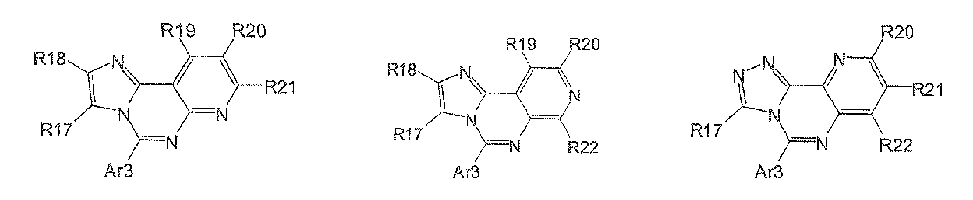


- The organic light emitting device according to claim 3, wherein the organic material layer comprising one or more selected from the group consisting of compounds represented by Formulas 1 to 4 is an electron transporting layer, an electron injection layer, or a layer which simultaneously transports and injects electrons.
- The organic light emitting device according to claim 1 or 3, wherein the compound having a fluorescent light emitting efficiency equal to or greater than the fluorescent light emitting efficiency of NPB is a compound represented by the following Formula 11:

Ar16 to Ar27 are the same as or different from each other and are each independently a substituted or unsubstituted aryl group having 6 to 50 carbon atoms, or a substituted or unsubstituted heteroaryl group having 5 to 50 carbon atoms, and Ar22 and Ar23, Ar24 and Ar25, or Ar26 and Ar27 may be connected to each other to form a saturated or unsaturated cyclic group, and
a, b, c, p, q, and r are each independently an integer of 0 to 3, but at least one of a, b, and c is not 0. - The organic light emitting device according to claim 1 or 3, wherein the compound having a fluorescent light emitting efficiency equal to or greater than the fluorescent light emitting efficiency of NPB is a compound represented by the following Formula 12:


Ar28 to Ar31 are the same as or different from each other and are each independently a substituted or unsubstituted aryl group having 6 to 50 carbon atoms, or a substituted or unsubstituted heteroaryl group having 5 to 50 carbon atoms, and Ar29 and Ar30 may be connected to each other to form a saturated or unsaturated cyclic group,
L1 is a direct bond, a substituted or unsubstituted arylene group having 6 to 50 carbon atoms, or a substituted or unsubstituted heteroarylene group having 5 to 50 carbon atoms, and
x is an integer of 0 to 5. - The organic light emitting device according to claim 1 or 3, wherein the compound having a fluorescent light emitting efficiency equal to or greater than the fluorescent light emitting efficiency of NPB is a compound represented by the following Formula 13:

L2 is a substituted or unsubstituted arylene group having 10 to 40 carbon atoms, and
Ar32 to Ar35 are the same as or different from each other and are each independently a substituted or unsubstituted aryl group having 6 to 50 carbon atoms, or a substituted or unsubstituted heteroaryl group having 5 to 50 carbon atoms, and Ar32 and Ar33 or Ar34 and Ar35 may be connected to each other, or one of Ar32 to Ar35 may be connected to L2 or a substituent group of L2 to form a saturated or unsaturated cyclic group. - The organic light emitting device according to claim 1 or 3, wherein the compound having a fluorescent light emitting efficiency equal to or greater than the fluorescent light emitting efficiency of NPB is a compound represented by the following Formula 14 or 15:


R1 to R12 are the same as or different from each other and are each independently selected from the group consisting of a hydrogen, a halogen, an alkyl group having I to 10 carbon atoms, an alkenyl group having 2 to 10 carbon atoms, an alkoxy group having 1 to 10 carbon atoms, an aryl group having 6 to 20 carbon atoms, and a heteroaryl group having 5 to 20 carbon atoms,
Ar1 and Ar2 are the same as or different from each other and are each independently selected from the group consisting of an aryl group having 6 to 20 carbon atoms and a heteroaryl group having 5 to 20 carbon atoms, and
m and n are each independently an integer of 0 to 4. - The organic light emitting device according to claim 1 or 3, wherein the compound having a fluorescent light emitting efficiency equal to or greater than the fluorescent light emitting efficiency of NPB is a compound represented by the following Formula 16:

X1 is an N-carbazolyl group that is unsubstituted or substituted by one or more selected from the group consisting of a halogen, an alkyl group having 1 to 10 carbon atoms, an alkoxy group having 1 to 10 carbon atoms, and an aryl group having 6 to 20 carbon atoms; an N-phenoxazyl group that is unsubstituted or substituted by one or more selected from the group consisting of a halogen, an alkyl group having 1 to 10 carbon atoms, an alkoxy group having 1 to 10 carbon atoms, and an aryl group having 6 to 20 carbon atoms; or an N-phenothiazyl group that is unsubstituted or substituted by one or more selected from the group consisting of a halogen, an alkyl group having 1 to 10 carbon atoms, an alkoxy group having 1 to 10 carbon atoms, and an aryl group having 6 to 20 carbon atoms,
X2 is an N-carbazolyl group that is unsubstituted or substituted by one or more selected from the group consisting of a halogen, an alkyl group having 1 to 10 carbon atoms, an alkoxy group having 1 to 10 carbon atoms, and an aryl group having 6 to 20 carbon atoms; an N-phenoxazyl group that is unsubstituted or substituted by one or more selected from the group consisting of a halogen, an alkyl group having 1 to 10 carbon atoms, an alkoxy group having 1 to 10 carbon atoms, and an aryl group having 6 to 20 carbon atoms; an N-phenothiazyl group that is unsubstituted or substituted by one or more selected from the group consisting of a halogen, an alkyl group having 1 to 10 carbon atoms, an alkoxy group having 1 to 10 carbon atoms, and an aryl group having 6 to 20 carbon atoms; or -NAr1Ar2, and
Ar1 and Ar2 are each independently an aryl group having 6 to 20 carbon atoms, which is unsubstituted or substituted by one or more selected from the group consisting of a halogen, an alkyl group, an alkoxy group, and an aryl group; or a heteroaryl group having 5 to 20 carbon atoms, which is unsubstituted or substituted by one or more selected from the group consisting of a halogen, an alkyl group, an alkoxy group, and an aryl group,
B1 and B2 are the same as or different from each other and are each independently a hydrogen; a deuterium; an alkyl group; an aryl group having 6 to 20 carbon atoms, which is unsubstituted or substituted by one or more selected from the group consisting of a halogen, an alkyl group, an alkoxy group, and an aryl group; a heteroaryl group having 5 to 20 carbon atoms, which is unsubstituted or substituted by one or more selected from the group consisting of a halogen, an alkyl group, an alkoxy group, and an aryl group; or an aralkyl group which is unsubstituted or substituted by one or more selected from the group consisting of a halogen, an alkyl group, an alkoxy group, and an aryl group, and
Z1 and Z2 are the same as or different from each other and are each independently a hydrogen; a deuterium; a halogen; an alkyl group; an alkoxy group; an aryl group having 6 to 20 carbon atoms, which is selected from the group consisting of a halogen, an alkyl group, an alkoxy group, and an aryl group; or a heteroaryl group having 5 to 20 carbon atoms, which is selected from the group consisting of a halogen, an alkyl group, an alkoxy group, and an aryl group. - The organic light emitting device according to claim 3, wherein the organic material layer comprising one or more compounds selected from the group consisting of compounds represented by Formulas 1 to 4 further comprises a reducing dopant.
- The organic light emitting device according to claim 1, wherein the organic material layer comprising a compound having a fluorescent light emitting efficiency equal to or greater than the fluorescent light emitting efficiency of NPB further comprises a p-type dopant.
- The organic light emitting device according to claim 1, wherein the light emitting layer comprises a phosphorescent material.
- The organic light emitting device of claim 1, wherein the organic material layer comprising a compound having a fluorescent light emitting efficiency equal to or greater than the fluorescent light emitting efficiency of NPB is a hole injection layer, a hole transporting layer, or a layer which simultaneously injects and transports holes.
Applications Claiming Priority (2)
| Application Number | Priority Date | Filing Date | Title |
|---|---|---|---|
| KR20100134759 | 2010-12-24 | ||
| PCT/KR2011/010043 WO2012087067A2 (en) | 2010-12-24 | 2011-12-23 | Organic light-emitting device and method for manufacturing same |
Publications (3)
| Publication Number | Publication Date |
|---|---|
| EP2657315A2 true EP2657315A2 (en) | 2013-10-30 |
| EP2657315A4 EP2657315A4 (en) | 2017-09-13 |
| EP2657315B1 EP2657315B1 (en) | 2020-12-16 |
Family
ID=46314667
Family Applications (1)
| Application Number | Title | Priority Date | Filing Date |
|---|---|---|---|
| EP11850159.2A Active EP2657315B1 (en) | 2010-12-24 | 2011-12-23 | Organic light-emitting device |
Country Status (7)
| Country | Link |
|---|---|
| US (1) | US9349964B2 (en) |
| EP (1) | EP2657315B1 (en) |
| JP (2) | JP5752806B2 (en) |
| KR (1) | KR101376933B1 (en) |
| CN (1) | CN103562342B (en) |
| TW (1) | TWI495707B (en) |
| WO (1) | WO2012087067A2 (en) |
Families Citing this family (92)
| Publication number | Priority date | Publication date | Assignee | Title |
|---|---|---|---|---|
| US8946695B2 (en) * | 2010-12-29 | 2015-02-03 | Lg Chem, Ltd. | Compound, and organic light-emitting device using same |
| JPWO2013061805A1 (en) * | 2011-10-24 | 2015-04-02 | 保土谷化学工業株式会社 | Novel triphenylene derivative and organic electroluminescence device using the derivative |
| WO2013118846A1 (en) | 2012-02-10 | 2013-08-15 | 出光興産株式会社 | Aromatic amine derivative, organic electroluminescent element and electronic device |
| KR101590229B1 (en) * | 2012-11-21 | 2016-02-01 | 주식회사 엘지화학 | Organic light emitting device material and organic light emitting device comprising the same |
| KR102102352B1 (en) * | 2013-01-30 | 2020-06-01 | 삼성디스플레이 주식회사 | An organic light emitting diode |
| CN107963972B (en) * | 2013-02-22 | 2021-09-03 | 保土谷化学工业株式会社 | Organic electroluminescent device |
| KR102191993B1 (en) | 2013-10-02 | 2020-12-17 | 삼성디스플레이 주식회사 | Organic compounds and organic light emitting device comprising the same |
| KR101772746B1 (en) * | 2014-08-12 | 2017-08-30 | 주식회사 엘지화학 | Organic light emitting diode |
| KR20160067034A (en) * | 2014-12-03 | 2016-06-13 | 주식회사 엘지화학 | Organic light emitting device |
| JP6519910B2 (en) * | 2014-12-11 | 2019-05-29 | 株式会社Joled | Organic EL element and method of manufacturing organic EL element |
| US9929361B2 (en) | 2015-02-16 | 2018-03-27 | Universal Display Corporation | Organic electroluminescent materials and devices |
| US11056657B2 (en) | 2015-02-27 | 2021-07-06 | University Display Corporation | Organic electroluminescent materials and devices |
| JP6552257B2 (en) | 2015-04-30 | 2019-07-31 | キヤノン株式会社 | 2,2'-bibenzo [d] imidazolidene compound having a heterocyclic monocyclic group at the 1-position, 1'-position, 3-position, 3'-position, organic light-emitting device having the same, and display device |
| US9859510B2 (en) | 2015-05-15 | 2018-01-02 | Universal Display Corporation | Organic electroluminescent materials and devices |
| US10418568B2 (en) | 2015-06-01 | 2019-09-17 | Universal Display Corporation | Organic electroluminescent materials and devices |
| CN107615489B (en) * | 2015-06-05 | 2020-08-11 | 佳能株式会社 | Organic photoelectric conversion element, optical area array sensor, imaging device and imaging device |
| US11127905B2 (en) | 2015-07-29 | 2021-09-21 | Universal Display Corporation | Organic electroluminescent materials and devices |
| US10672996B2 (en) | 2015-09-03 | 2020-06-02 | Universal Display Corporation | Organic electroluminescent materials and devices |
| US20170229663A1 (en) | 2016-02-09 | 2017-08-10 | Universal Display Corporation | Organic electroluminescent materials and devices |
| US10236456B2 (en) | 2016-04-11 | 2019-03-19 | Universal Display Corporation | Organic electroluminescent materials and devices |
| KR102479135B1 (en) * | 2016-04-18 | 2022-12-21 | 롬엔드하스전자재료코리아유한회사 | A plurality of host materials and organic electroluminescent device comprising the same |
| US10862054B2 (en) | 2016-06-20 | 2020-12-08 | Universal Display Corporation | Organic electroluminescent materials and devices |
| US10672997B2 (en) | 2016-06-20 | 2020-06-02 | Universal Display Corporation | Organic electroluminescent materials and devices |
| US11482683B2 (en) | 2016-06-20 | 2022-10-25 | Universal Display Corporation | Organic electroluminescent materials and devices |
| US10608186B2 (en) | 2016-09-14 | 2020-03-31 | Universal Display Corporation | Organic electroluminescent materials and devices |
| US10680187B2 (en) | 2016-09-23 | 2020-06-09 | Universal Display Corporation | Organic electroluminescent materials and devices |
| US11196010B2 (en) | 2016-10-03 | 2021-12-07 | Universal Display Corporation | Organic electroluminescent materials and devices |
| US11011709B2 (en) | 2016-10-07 | 2021-05-18 | Universal Display Corporation | Organic electroluminescent materials and devices |
| US12317745B2 (en) | 2016-11-09 | 2025-05-27 | Universal Display Corporation | Organic electroluminescent materials and devices |
| US10680188B2 (en) | 2016-11-11 | 2020-06-09 | Universal Display Corporation | Organic electroluminescent materials and devices |
| US11780865B2 (en) | 2017-01-09 | 2023-10-10 | Universal Display Corporation | Organic electroluminescent materials and devices |
| US10844085B2 (en) | 2017-03-29 | 2020-11-24 | Universal Display Corporation | Organic electroluminescent materials and devices |
| US10944060B2 (en) | 2017-05-11 | 2021-03-09 | Universal Display Corporation | Organic electroluminescent materials and devices |
| US12098157B2 (en) | 2017-06-23 | 2024-09-24 | Universal Display Corporation | Organic electroluminescent materials and devices |
| US11228010B2 (en) | 2017-07-26 | 2022-01-18 | Universal Display Corporation | Organic electroluminescent materials and devices |
| US11744142B2 (en) | 2017-08-10 | 2023-08-29 | Universal Display Corporation | Organic electroluminescent materials and devices |
| JP7418323B2 (en) | 2017-08-24 | 2024-01-19 | ザ ユナイテッド ステイツ オブ アメリカ, アズ リプレゼンテッド バイ ザ セクレタリー, デパートメント オブ ヘルス アンド ヒューマン サービシーズ | Conformational constraints of cyanine fluorophores in the far-red and near-IR ranges |
| US12180230B2 (en) | 2017-11-28 | 2024-12-31 | University Of Southern California | Carbene compounds and organic electroluminescent devices |
| EP3492480B1 (en) | 2017-11-29 | 2021-10-20 | Universal Display Corporation | Organic electroluminescent materials and devices |
| US11937503B2 (en) | 2017-11-30 | 2024-03-19 | Universal Display Corporation | Organic electroluminescent materials and devices |
| US11542289B2 (en) | 2018-01-26 | 2023-01-03 | Universal Display Corporation | Organic electroluminescent materials and devices |
| US11165028B2 (en) | 2018-03-12 | 2021-11-02 | Universal Display Corporation | Organic electroluminescent materials and devices |
| US12453279B2 (en) | 2018-08-22 | 2025-10-21 | Universal Display Corporation | Organic electroluminescent materials and devices |
| US11737349B2 (en) | 2018-12-12 | 2023-08-22 | Universal Display Corporation | Organic electroluminescent materials and devices |
| CN111366643B (en) * | 2018-12-25 | 2022-08-19 | 广东阿格蕾雅光电材料有限公司 | Detection method of OLED material intermediate |
| US11780829B2 (en) | 2019-01-30 | 2023-10-10 | The University Of Southern California | Organic electroluminescent materials and devices |
| US12477890B2 (en) | 2019-02-01 | 2025-11-18 | Universal Display Corporation | Organic electroluminescent materials and devices |
| JP2020158491A (en) | 2019-03-26 | 2020-10-01 | ユニバーサル ディスプレイ コーポレイション | Organic electroluminescence materials and devices |
| US12281128B2 (en) | 2019-07-30 | 2025-04-22 | Universal Display Corporation | Organic electroluminescent materials and devices |
| US12139501B2 (en) | 2019-08-16 | 2024-11-12 | Universal Display Corporation | Organic electroluminescent materials and devices |
| US20210135130A1 (en) | 2019-11-04 | 2021-05-06 | Universal Display Corporation | Organic electroluminescent materials and devices |
| US12538698B2 (en) | 2020-01-06 | 2026-01-27 | Universal Display Corporation | Organic electroluminescent materials and devices |
| US12426495B2 (en) | 2020-01-28 | 2025-09-23 | Universal Display Corporation | Organic electroluminescent materials and devices |
| EP3937268B1 (en) | 2020-07-10 | 2025-05-07 | Universal Display Corporation | Plasmonic oleds and vertical dipole emitters |
| US12187748B2 (en) | 2020-11-02 | 2025-01-07 | Universal Display Corporation | Organic electroluminescent materials and devices |
| US20220158096A1 (en) | 2020-11-16 | 2022-05-19 | Universal Display Corporation | Organic electroluminescent materials and devices |
| US20220165967A1 (en) | 2020-11-24 | 2022-05-26 | Universal Display Corporation | Organic electroluminescent materials and devices |
| US12325717B2 (en) | 2020-11-24 | 2025-06-10 | Universal Display Corporation | Organic electroluminescent materials and devices |
| US12575316B2 (en) | 2021-02-03 | 2026-03-10 | Universal Display Corporation | Organic electroluminescent materials and devices |
| EP4060758A3 (en) | 2021-02-26 | 2023-03-29 | Universal Display Corporation | Organic electroluminescent materials and devices |
| EP4723858A2 (en) | 2021-02-26 | 2026-04-08 | Universal Display Corporation | Organic electroluminescent materials and devices |
| US12606582B2 (en) | 2021-03-05 | 2026-04-21 | Universal Display Corporation | Organic electroluminescent materials and devices |
| US12428599B2 (en) | 2021-03-09 | 2025-09-30 | Universal Display Corporation | Organic electroluminescent materials and devices |
| US20220298190A1 (en) | 2021-03-12 | 2022-09-22 | Universal Display Corporation | Organic electroluminescent materials and devices |
| US12421262B2 (en) | 2021-03-15 | 2025-09-23 | Universal Display Corporation | Organic electroluminescent materials and devices |
| US20220340607A1 (en) | 2021-04-05 | 2022-10-27 | Universal Display Corporation | Organic electroluminescent materials and devices |
| US12480042B2 (en) | 2021-04-09 | 2025-11-25 | Universal Display Corporation | Organic electroluminescent materials and devices |
| EP4075531A1 (en) | 2021-04-13 | 2022-10-19 | Universal Display Corporation | Plasmonic oleds and vertical dipole emitters |
| US20220352478A1 (en) | 2021-04-14 | 2022-11-03 | Universal Display Corporation | Organic eletroluminescent materials and devices |
| US20230006149A1 (en) | 2021-04-23 | 2023-01-05 | Universal Display Corporation | Organic electroluminescent materials and devices |
| US20220407020A1 (en) | 2021-04-23 | 2022-12-22 | Universal Display Corporation | Organic electroluminescent materials and devices |
| US20230133787A1 (en) | 2021-06-08 | 2023-05-04 | University Of Southern California | Molecular Alignment of Homoleptic Iridium Phosphors |
| US12550611B2 (en) | 2021-08-03 | 2026-02-10 | Universal Display Corporation | Organic electroluminescent materials and devices |
| EP4151699A1 (en) | 2021-09-17 | 2023-03-22 | Universal Display Corporation | Organic electroluminescent materials and devices |
| US12473318B2 (en) | 2021-10-08 | 2025-11-18 | Universal Display Corporation | Organic electroluminescent materials and devices |
| US12509628B2 (en) | 2021-12-16 | 2025-12-30 | Universal Display Corporation | Organic electroluminescent materials and devices |
| EP4231804A3 (en) | 2022-02-16 | 2023-09-20 | Universal Display Corporation | Organic electroluminescent materials and devices |
| US20230292592A1 (en) | 2022-03-09 | 2023-09-14 | Universal Display Corporation | Organic electroluminescent materials and devices |
| US20230337516A1 (en) | 2022-04-18 | 2023-10-19 | Universal Display Corporation | Organic electroluminescent materials and devices |
| US20230389421A1 (en) | 2022-05-24 | 2023-11-30 | Universal Display Corporation | Organic electroluminescent materials and devices |
| EP4293001A1 (en) | 2022-06-08 | 2023-12-20 | Universal Display Corporation | Organic electroluminescent materials and devices |
| US20240016051A1 (en) | 2022-06-28 | 2024-01-11 | Universal Display Corporation | Organic electroluminescent materials and devices |
| US20240107880A1 (en) | 2022-08-17 | 2024-03-28 | Universal Display Corporation | Organic electroluminescent materials and devices |
| US20240196730A1 (en) | 2022-10-27 | 2024-06-13 | Universal Display Corporation | Organic electroluminescent materials and devices |
| US20240188316A1 (en) | 2022-10-27 | 2024-06-06 | Universal Display Corporation | Organic electroluminescent materials and devices |
| US20240188419A1 (en) | 2022-10-27 | 2024-06-06 | Universal Display Corporation | Organic electroluminescent materials and devices |
| US20240188319A1 (en) | 2022-10-27 | 2024-06-06 | Universal Display Corporation | Organic electroluminescent materials and devices |
| US20240180025A1 (en) | 2022-10-27 | 2024-05-30 | Universal Display Corporation | Organic electroluminescent materials and devices |
| US20240247017A1 (en) | 2022-12-14 | 2024-07-25 | Universal Display Corporation | Organic electroluminescent materials and devices |
| KR20240152438A (en) | 2023-04-12 | 2024-10-22 | 삼성디스플레이 주식회사 | Display device |
| US20250204239A1 (en) | 2023-12-15 | 2025-06-19 | Universal Display Corporation | Organic electroluminescent materials and devices |
| US20250204238A1 (en) | 2023-12-15 | 2025-06-19 | Universal Display Corporation | Organic electroluminscent materials and devices |
Family Cites Families (25)
| Publication number | Priority date | Publication date | Assignee | Title |
|---|---|---|---|---|
| US6242115B1 (en) | 1997-09-08 | 2001-06-05 | The University Of Southern California | OLEDs containing thermally stable asymmetric charge carrier materials |
| JP3856546B2 (en) | 1997-11-11 | 2006-12-13 | 三井化学株式会社 | Organic electroluminescence device |
| DE60229934D1 (en) | 2001-05-24 | 2009-01-02 | Idemitsu Kosan Co | ORGANIC ELECTROLUMINESCENCE ELEMENT |
| KR100691543B1 (en) | 2002-01-18 | 2007-03-09 | 주식회사 엘지화학 | New material for electron transport and organic light emitting device using the same |
| JP4442114B2 (en) * | 2002-05-14 | 2010-03-31 | コニカミノルタホールディングス株式会社 | Organic electroluminescence element and display device |
| KR100830332B1 (en) | 2005-11-30 | 2008-05-19 | 삼성에스디아이 주식회사 | Organic light-emitting device |
| KR100864364B1 (en) | 2005-12-13 | 2008-10-17 | 주식회사 엘지화학 | Novel imidazoquinazoline derivative, process for preparing the same, and organic electronic device using the same |
| WO2007148660A1 (en) * | 2006-06-22 | 2007-12-27 | Idemitsu Kosan Co., Ltd. | Organic electroluminescent device employing heterocycle-containing arylamine derivative |
| KR100893044B1 (en) | 2006-07-26 | 2009-04-15 | 주식회사 엘지화학 | Anthracene derivative, organic electronic device using the same, and electronic device including the organic electronic device |
| TW200908777A (en) | 2007-03-23 | 2009-02-16 | Idemitsu Kosan Co | Organic el device |
| JP2009076817A (en) * | 2007-09-25 | 2009-04-09 | Sony Corp | Organic electroluminescence device and display device |
| EP2224510A1 (en) * | 2007-12-21 | 2010-09-01 | Idemitsu Kosan Co., Ltd. | Organic electroluminescent device |
| JP5304010B2 (en) * | 2008-04-23 | 2013-10-02 | コニカミノルタ株式会社 | Organic electroluminescence element, display device and lighting device |
| TWI498412B (en) * | 2008-05-16 | 2015-09-01 | Hodogaya Chemical Co Ltd | Arylamine compound |
| JP5631559B2 (en) * | 2008-05-16 | 2014-11-26 | 株式会社半導体エネルギー研究所 | Aromatic amine compound and light emitting device |
| KR101115154B1 (en) | 2008-05-23 | 2012-02-24 | 주식회사 엘지화학 | Organic light emitting diode and method for fabricating the same |
| US9587172B2 (en) * | 2008-10-01 | 2017-03-07 | Lg Display Co., Ltd. | Organic light-emitting diode and method of manufacturing the same |
| JP5801193B2 (en) | 2008-11-03 | 2015-10-28 | エルジー・ケム・リミテッド | New nitrogen-containing heterocyclic compounds and organic electronic devices using the same |
| JP5701766B2 (en) | 2008-11-11 | 2015-04-15 | メルク パテント ゲーエムベーハー | Organic electroluminescent device |
| JP2010165977A (en) | 2009-01-19 | 2010-07-29 | Sony Corp | Organic electroluminescent element, display and electronic equipment |
| DE102009005746A1 (en) | 2009-01-23 | 2010-07-29 | Merck Patent Gmbh | Materials for organic electroluminescent devices |
| JP5509634B2 (en) * | 2009-03-16 | 2014-06-04 | コニカミノルタ株式会社 | ORGANIC ELECTROLUMINESCENT ELEMENT, DISPLAY DEVICE, LIGHTING DEVICE, AND ORGANIC ELECTROLUMINESCENT ELEMENT MATERIAL |
| US20120091438A1 (en) | 2009-04-01 | 2012-04-19 | Idemitsu Kosan Co., Ltd. | Organic electroluminescent element |
| JP5347662B2 (en) * | 2009-04-03 | 2013-11-20 | ソニー株式会社 | Organic electroluminescence device and display device |
| DE102009023155A1 (en) | 2009-05-29 | 2010-12-02 | Merck Patent Gmbh | Materials for organic electroluminescent devices |
-
2011
- 2011-12-22 US US13/335,165 patent/US9349964B2/en active Active
- 2011-12-23 WO PCT/KR2011/010043 patent/WO2012087067A2/en not_active Ceased
- 2011-12-23 TW TW100148411A patent/TWI495707B/en active
- 2011-12-23 EP EP11850159.2A patent/EP2657315B1/en active Active
- 2011-12-23 JP JP2013546033A patent/JP5752806B2/en active Active
- 2011-12-23 KR KR1020110141360A patent/KR101376933B1/en active Active
- 2011-12-23 CN CN201180068531.9A patent/CN103562342B/en active Active
-
2015
- 2015-02-19 JP JP2015030602A patent/JP2015133503A/en active Pending
Non-Patent Citations (1)
| Title |
|---|
| See references of WO2012087067A3 * |
Also Published As
| Publication number | Publication date |
|---|---|
| US9349964B2 (en) | 2016-05-24 |
| CN103562342A (en) | 2014-02-05 |
| KR20120073144A (en) | 2012-07-04 |
| JP5752806B2 (en) | 2015-07-22 |
| WO2012087067A9 (en) | 2012-09-07 |
| JP2015133503A (en) | 2015-07-23 |
| KR101376933B1 (en) | 2014-03-27 |
| WO2012087067A2 (en) | 2012-06-28 |
| US20120193612A1 (en) | 2012-08-02 |
| CN103562342B (en) | 2017-02-15 |
| EP2657315B1 (en) | 2020-12-16 |
| TWI495707B (en) | 2015-08-11 |
| JP2014507789A (en) | 2014-03-27 |
| WO2012087067A3 (en) | 2012-10-26 |
| EP2657315A4 (en) | 2017-09-13 |
| TW201241150A (en) | 2012-10-16 |
Similar Documents
| Publication | Publication Date | Title |
|---|---|---|
| EP2657315B1 (en) | Organic light-emitting device | |
| KR101614403B1 (en) | White oled with blue light-emitting layers | |
| KR101668044B1 (en) | Oled with high efficiency blue light-emitting layer | |
| KR101595433B1 (en) | Tandem white oled with efficient electron transfer | |
| JP5213405B2 (en) | Organic electroluminescence device | |
| US20060040131A1 (en) | OLEDs with improved operational lifetime | |
| CN105849930A (en) | Organic light-emitting element | |
| EP2183799B1 (en) | High-performance broadband oled device | |
| EP1755362B1 (en) | Organic el device | |
| EP4033556B1 (en) | Organic electroluminescent device | |
| KR20140020260A (en) | Organic electroluminescent element | |
| CN110492007A (en) | A kind of acridine compounds and its application in organic electroluminescence devices | |
| JP5277588B2 (en) | Organic EL device | |
| TWI394483B (en) | Oled device with stabilized green light-emitting layer | |
| US7195829B2 (en) | Organic element for electroluminescent devices | |
| JP2009010181A (en) | Light emitting element | |
| KR102673123B1 (en) | Organic electroluminescent device | |
| KR102745953B1 (en) | Organic electroluminescent device | |
| KR20240156557A (en) | Novel organic compound and materials for organic electroluminescent devices comprising the same and organic electroluminescent devices comprising the same | |
| JP2019102644A (en) | Organic electroluminescent element |
Legal Events
| Date | Code | Title | Description |
|---|---|---|---|
| PUAI | Public reference made under article 153(3) epc to a published international application that has entered the european phase |
Free format text: ORIGINAL CODE: 0009012 |
|
| 17P | Request for examination filed |
Effective date: 20130620 |
|
| AK | Designated contracting states |
Kind code of ref document: A2 Designated state(s): AL AT BE BG CH CY CZ DE DK EE ES FI FR GB GR HR HU IE IS IT LI LT LU LV MC MK MT NL NO PL PT RO RS SE SI SK SM TR |
|
| DAX | Request for extension of the european patent (deleted) | ||
| RIC1 | Information provided on ipc code assigned before grant |
Ipc: H01L 51/54 20060101ALI20170313BHEP Ipc: C09K 11/06 20060101AFI20170313BHEP |
|
| A4 | Supplementary search report drawn up and despatched |
Effective date: 20170816 |
|
| RIC1 | Information provided on ipc code assigned before grant |
Ipc: H01L 51/54 20060101ALI20170809BHEP Ipc: C09K 11/06 20060101AFI20170809BHEP |
|
| RAP1 | Party data changed (applicant data changed or rights of an application transferred) |
Owner name: LG CHEM, LTD. |
|
| STAA | Information on the status of an ep patent application or granted ep patent |
Free format text: STATUS: EXAMINATION IS IN PROGRESS |
|
| 17Q | First examination report despatched |
Effective date: 20191108 |
|
| GRAP | Despatch of communication of intention to grant a patent |
Free format text: ORIGINAL CODE: EPIDOSNIGR1 |
|
| STAA | Information on the status of an ep patent application or granted ep patent |
Free format text: STATUS: GRANT OF PATENT IS INTENDED |
|
| INTG | Intention to grant announced |
Effective date: 20200910 |
|
| GRAS | Grant fee paid |
Free format text: ORIGINAL CODE: EPIDOSNIGR3 |
|
| GRAA | (expected) grant |
Free format text: ORIGINAL CODE: 0009210 |
|
| STAA | Information on the status of an ep patent application or granted ep patent |
Free format text: STATUS: THE PATENT HAS BEEN GRANTED |
|
| AK | Designated contracting states |
Kind code of ref document: B1 Designated state(s): AL AT BE BG CH CY CZ DE DK EE ES FI FR GB GR HR HU IE IS IT LI LT LU LV MC MK MT NL NO PL PT RO RS SE SI SK SM TR |
|
| REG | Reference to a national code |
Ref country code: GB Ref legal event code: FG4D |
|
| REG | Reference to a national code |
Ref country code: DE Ref legal event code: R096 Ref document number: 602011069683 Country of ref document: DE |
|
| REG | Reference to a national code |
Ref country code: IE Ref legal event code: FG4D |
|
| REG | Reference to a national code |
Ref country code: AT Ref legal event code: REF Ref document number: 1345592 Country of ref document: AT Kind code of ref document: T Effective date: 20210115 |
|
| PG25 | Lapsed in a contracting state [announced via postgrant information from national office to epo] |
Ref country code: GR Free format text: LAPSE BECAUSE OF FAILURE TO SUBMIT A TRANSLATION OF THE DESCRIPTION OR TO PAY THE FEE WITHIN THE PRESCRIBED TIME-LIMIT Effective date: 20210317 Ref country code: NO Free format text: LAPSE BECAUSE OF FAILURE TO SUBMIT A TRANSLATION OF THE DESCRIPTION OR TO PAY THE FEE WITHIN THE PRESCRIBED TIME-LIMIT Effective date: 20210316 Ref country code: FI Free format text: LAPSE BECAUSE OF FAILURE TO SUBMIT A TRANSLATION OF THE DESCRIPTION OR TO PAY THE FEE WITHIN THE PRESCRIBED TIME-LIMIT Effective date: 20201216 Ref country code: RS Free format text: LAPSE BECAUSE OF FAILURE TO SUBMIT A TRANSLATION OF THE DESCRIPTION OR TO PAY THE FEE WITHIN THE PRESCRIBED TIME-LIMIT Effective date: 20201216 |
|
| REG | Reference to a national code |
Ref country code: AT Ref legal event code: MK05 Ref document number: 1345592 Country of ref document: AT Kind code of ref document: T Effective date: 20201216 |
|
| REG | Reference to a national code |
Ref country code: NL Ref legal event code: MP Effective date: 20201216 |
|
| PG25 | Lapsed in a contracting state [announced via postgrant information from national office to epo] |
Ref country code: SE Free format text: LAPSE BECAUSE OF FAILURE TO SUBMIT A TRANSLATION OF THE DESCRIPTION OR TO PAY THE FEE WITHIN THE PRESCRIBED TIME-LIMIT Effective date: 20201216 Ref country code: LV Free format text: LAPSE BECAUSE OF FAILURE TO SUBMIT A TRANSLATION OF THE DESCRIPTION OR TO PAY THE FEE WITHIN THE PRESCRIBED TIME-LIMIT Effective date: 20201216 Ref country code: BG Free format text: LAPSE BECAUSE OF FAILURE TO SUBMIT A TRANSLATION OF THE DESCRIPTION OR TO PAY THE FEE WITHIN THE PRESCRIBED TIME-LIMIT Effective date: 20210316 |
|
| PG25 | Lapsed in a contracting state [announced via postgrant information from national office to epo] |
Ref country code: NL Free format text: LAPSE BECAUSE OF FAILURE TO SUBMIT A TRANSLATION OF THE DESCRIPTION OR TO PAY THE FEE WITHIN THE PRESCRIBED TIME-LIMIT Effective date: 20201216 Ref country code: HR Free format text: LAPSE BECAUSE OF FAILURE TO SUBMIT A TRANSLATION OF THE DESCRIPTION OR TO PAY THE FEE WITHIN THE PRESCRIBED TIME-LIMIT Effective date: 20201216 |
|
| REG | Reference to a national code |
Ref country code: LT Ref legal event code: MG9D |
|
| PG25 | Lapsed in a contracting state [announced via postgrant information from national office to epo] |
Ref country code: LT Free format text: LAPSE BECAUSE OF FAILURE TO SUBMIT A TRANSLATION OF THE DESCRIPTION OR TO PAY THE FEE WITHIN THE PRESCRIBED TIME-LIMIT Effective date: 20201216 Ref country code: RO Free format text: LAPSE BECAUSE OF FAILURE TO SUBMIT A TRANSLATION OF THE DESCRIPTION OR TO PAY THE FEE WITHIN THE PRESCRIBED TIME-LIMIT Effective date: 20201216 Ref country code: SK Free format text: LAPSE BECAUSE OF FAILURE TO SUBMIT A TRANSLATION OF THE DESCRIPTION OR TO PAY THE FEE WITHIN THE PRESCRIBED TIME-LIMIT Effective date: 20201216 Ref country code: PT Free format text: LAPSE BECAUSE OF FAILURE TO SUBMIT A TRANSLATION OF THE DESCRIPTION OR TO PAY THE FEE WITHIN THE PRESCRIBED TIME-LIMIT Effective date: 20210416 Ref country code: SM Free format text: LAPSE BECAUSE OF FAILURE TO SUBMIT A TRANSLATION OF THE DESCRIPTION OR TO PAY THE FEE WITHIN THE PRESCRIBED TIME-LIMIT Effective date: 20201216 Ref country code: CZ Free format text: LAPSE BECAUSE OF FAILURE TO SUBMIT A TRANSLATION OF THE DESCRIPTION OR TO PAY THE FEE WITHIN THE PRESCRIBED TIME-LIMIT Effective date: 20201216 Ref country code: EE Free format text: LAPSE BECAUSE OF FAILURE TO SUBMIT A TRANSLATION OF THE DESCRIPTION OR TO PAY THE FEE WITHIN THE PRESCRIBED TIME-LIMIT Effective date: 20201216 |
|
| REG | Reference to a national code |
Ref country code: CH Ref legal event code: PL |
|
| PG25 | Lapsed in a contracting state [announced via postgrant information from national office to epo] |
Ref country code: AT Free format text: LAPSE BECAUSE OF FAILURE TO SUBMIT A TRANSLATION OF THE DESCRIPTION OR TO PAY THE FEE WITHIN THE PRESCRIBED TIME-LIMIT Effective date: 20201216 Ref country code: PL Free format text: LAPSE BECAUSE OF FAILURE TO SUBMIT A TRANSLATION OF THE DESCRIPTION OR TO PAY THE FEE WITHIN THE PRESCRIBED TIME-LIMIT Effective date: 20201216 |
|
| REG | Reference to a national code |
Ref country code: BE Ref legal event code: MM Effective date: 20201231 |
|
| REG | Reference to a national code |
Ref country code: DE Ref legal event code: R097 Ref document number: 602011069683 Country of ref document: DE |
|
| PG25 | Lapsed in a contracting state [announced via postgrant information from national office to epo] |
Ref country code: MC Free format text: LAPSE BECAUSE OF FAILURE TO SUBMIT A TRANSLATION OF THE DESCRIPTION OR TO PAY THE FEE WITHIN THE PRESCRIBED TIME-LIMIT Effective date: 20201216 Ref country code: IS Free format text: LAPSE BECAUSE OF FAILURE TO SUBMIT A TRANSLATION OF THE DESCRIPTION OR TO PAY THE FEE WITHIN THE PRESCRIBED TIME-LIMIT Effective date: 20210416 |
|
| PLBE | No opposition filed within time limit |
Free format text: ORIGINAL CODE: 0009261 |
|
| STAA | Information on the status of an ep patent application or granted ep patent |
Free format text: STATUS: NO OPPOSITION FILED WITHIN TIME LIMIT |
|
| PG25 | Lapsed in a contracting state [announced via postgrant information from national office to epo] |
Ref country code: AL Free format text: LAPSE BECAUSE OF FAILURE TO SUBMIT A TRANSLATION OF THE DESCRIPTION OR TO PAY THE FEE WITHIN THE PRESCRIBED TIME-LIMIT Effective date: 20201216 Ref country code: IE Free format text: LAPSE BECAUSE OF NON-PAYMENT OF DUE FEES Effective date: 20201223 Ref country code: IT Free format text: LAPSE BECAUSE OF FAILURE TO SUBMIT A TRANSLATION OF THE DESCRIPTION OR TO PAY THE FEE WITHIN THE PRESCRIBED TIME-LIMIT Effective date: 20201216 Ref country code: LU Free format text: LAPSE BECAUSE OF NON-PAYMENT OF DUE FEES Effective date: 20201223 |
|
| 26N | No opposition filed |
Effective date: 20210917 |
|
| PG25 | Lapsed in a contracting state [announced via postgrant information from national office to epo] |
Ref country code: LI Free format text: LAPSE BECAUSE OF NON-PAYMENT OF DUE FEES Effective date: 20201231 Ref country code: CH Free format text: LAPSE BECAUSE OF NON-PAYMENT OF DUE FEES Effective date: 20201231 Ref country code: ES Free format text: LAPSE BECAUSE OF FAILURE TO SUBMIT A TRANSLATION OF THE DESCRIPTION OR TO PAY THE FEE WITHIN THE PRESCRIBED TIME-LIMIT Effective date: 20201216 Ref country code: DK Free format text: LAPSE BECAUSE OF FAILURE TO SUBMIT A TRANSLATION OF THE DESCRIPTION OR TO PAY THE FEE WITHIN THE PRESCRIBED TIME-LIMIT Effective date: 20201216 |
|
| PG25 | Lapsed in a contracting state [announced via postgrant information from national office to epo] |
Ref country code: SI Free format text: LAPSE BECAUSE OF FAILURE TO SUBMIT A TRANSLATION OF THE DESCRIPTION OR TO PAY THE FEE WITHIN THE PRESCRIBED TIME-LIMIT Effective date: 20201216 |
|
| PG25 | Lapsed in a contracting state [announced via postgrant information from national office to epo] |
Ref country code: IS Free format text: LAPSE BECAUSE OF FAILURE TO SUBMIT A TRANSLATION OF THE DESCRIPTION OR TO PAY THE FEE WITHIN THE PRESCRIBED TIME-LIMIT Effective date: 20210416 Ref country code: TR Free format text: LAPSE BECAUSE OF FAILURE TO SUBMIT A TRANSLATION OF THE DESCRIPTION OR TO PAY THE FEE WITHIN THE PRESCRIBED TIME-LIMIT Effective date: 20201216 Ref country code: MT Free format text: LAPSE BECAUSE OF FAILURE TO SUBMIT A TRANSLATION OF THE DESCRIPTION OR TO PAY THE FEE WITHIN THE PRESCRIBED TIME-LIMIT Effective date: 20201216 Ref country code: CY Free format text: LAPSE BECAUSE OF FAILURE TO SUBMIT A TRANSLATION OF THE DESCRIPTION OR TO PAY THE FEE WITHIN THE PRESCRIBED TIME-LIMIT Effective date: 20201216 |
|
| PG25 | Lapsed in a contracting state [announced via postgrant information from national office to epo] |
Ref country code: MK Free format text: LAPSE BECAUSE OF FAILURE TO SUBMIT A TRANSLATION OF THE DESCRIPTION OR TO PAY THE FEE WITHIN THE PRESCRIBED TIME-LIMIT Effective date: 20201216 |
|
| PG25 | Lapsed in a contracting state [announced via postgrant information from national office to epo] |
Ref country code: BE Free format text: LAPSE BECAUSE OF NON-PAYMENT OF DUE FEES Effective date: 20201231 |
|
| P01 | Opt-out of the competence of the unified patent court (upc) registered |
Effective date: 20230523 |
|
| PGFP | Annual fee paid to national office [announced via postgrant information from national office to epo] |
Ref country code: DE Payment date: 20251120 Year of fee payment: 15 |
|
| PGFP | Annual fee paid to national office [announced via postgrant information from national office to epo] |
Ref country code: GB Payment date: 20251120 Year of fee payment: 15 |
|
| PGFP | Annual fee paid to national office [announced via postgrant information from national office to epo] |
Ref country code: FR Payment date: 20251125 Year of fee payment: 15 |