EP2651087A1 - IQ mismatch compensation - Google Patents
IQ mismatch compensation Download PDFInfo
- Publication number
- EP2651087A1 EP2651087A1 EP12163662.5A EP12163662A EP2651087A1 EP 2651087 A1 EP2651087 A1 EP 2651087A1 EP 12163662 A EP12163662 A EP 12163662A EP 2651087 A1 EP2651087 A1 EP 2651087A1
- Authority
- EP
- European Patent Office
- Prior art keywords
- signal
- digital
- compensation
- phase
- path
- Prior art date
- Legal status (The legal status is an assumption and is not a legal conclusion. Google has not performed a legal analysis and makes no representation as to the accuracy of the status listed.)
- Granted
Links
- 230000008859 change Effects 0.000 claims abstract description 19
- 239000011159 matrix material Substances 0.000 claims description 54
- 238000000034 method Methods 0.000 claims description 23
- 238000009499 grossing Methods 0.000 claims description 7
- 230000006870 function Effects 0.000 description 16
- 230000010363 phase shift Effects 0.000 description 4
- 102000048176 Prostaglandin-D synthases Human genes 0.000 description 2
- 108030003866 Prostaglandin-D synthases Proteins 0.000 description 2
- 238000004590 computer program Methods 0.000 description 2
- 238000012986 modification Methods 0.000 description 2
- 230000004048 modification Effects 0.000 description 2
- 238000012545 processing Methods 0.000 description 2
- 238000000926 separation method Methods 0.000 description 2
- 230000003044 adaptive effect Effects 0.000 description 1
- 238000012937 correction Methods 0.000 description 1
- 230000008878 coupling Effects 0.000 description 1
- 238000010168 coupling process Methods 0.000 description 1
- 238000005859 coupling reaction Methods 0.000 description 1
- 230000001186 cumulative effect Effects 0.000 description 1
- 230000003287 optical effect Effects 0.000 description 1
- 230000008569 process Effects 0.000 description 1
- 238000012549 training Methods 0.000 description 1
Images

Classifications
-
- H—ELECTRICITY
- H04—ELECTRIC COMMUNICATION TECHNIQUE
- H04L—TRANSMISSION OF DIGITAL INFORMATION, e.g. TELEGRAPHIC COMMUNICATION
- H04L27/00—Modulated-carrier systems
- H04L27/10—Frequency-modulated carrier systems, i.e. using frequency-shift keying
- H04L27/14—Demodulator circuits; Receiver circuits
- H04L27/144—Demodulator circuits; Receiver circuits with demodulation using spectral properties of the received signal, e.g. by using frequency selective- or frequency sensitive elements
- H04L27/152—Demodulator circuits; Receiver circuits with demodulation using spectral properties of the received signal, e.g. by using frequency selective- or frequency sensitive elements using controlled oscillators, e.g. PLL arrangements
- H04L27/1525—Demodulator circuits; Receiver circuits with demodulation using spectral properties of the received signal, e.g. by using frequency selective- or frequency sensitive elements using controlled oscillators, e.g. PLL arrangements using quadrature demodulation
-
- H—ELECTRICITY
- H03—ELECTRONIC CIRCUITRY
- H03D—DEMODULATION OR TRANSFERENCE OF MODULATION FROM ONE CARRIER TO ANOTHER
- H03D3/00—Demodulation of angle-, frequency- or phase- modulated oscillations
- H03D3/007—Demodulation of angle-, frequency- or phase- modulated oscillations by converting the oscillations into two quadrature related signals
- H03D3/009—Compensating quadrature phase or amplitude imbalances
-
- H—ELECTRICITY
- H04—ELECTRIC COMMUNICATION TECHNIQUE
- H04B—TRANSMISSION
- H04B1/00—Details of transmission systems, not covered by a single one of groups H04B3/00 - H04B13/00; Details of transmission systems not characterised by the medium used for transmission
- H04B1/06—Receivers
- H04B1/10—Means associated with receiver for limiting or suppressing noise or interference
- H04B1/12—Neutralising, balancing, or compensation arrangements
- H04B1/123—Neutralising, balancing, or compensation arrangements using adaptive balancing or compensation means
-
- H—ELECTRICITY
- H04—ELECTRIC COMMUNICATION TECHNIQUE
- H04L—TRANSMISSION OF DIGITAL INFORMATION, e.g. TELEGRAPHIC COMMUNICATION
- H04L27/00—Modulated-carrier systems
- H04L27/32—Carrier systems characterised by combinations of two or more of the types covered by groups H04L27/02, H04L27/10, H04L27/18 or H04L27/26
- H04L27/34—Amplitude- and phase-modulated carrier systems, e.g. quadrature-amplitude modulated carrier systems
- H04L27/38—Demodulator circuits; Receiver circuits
- H04L27/3845—Demodulator circuits; Receiver circuits using non - coherent demodulation, i.e. not using a phase synchronous carrier
- H04L27/3854—Demodulator circuits; Receiver circuits using non - coherent demodulation, i.e. not using a phase synchronous carrier using a non - coherent carrier, including systems with baseband correction for phase or frequency offset
- H04L27/3863—Compensation for quadrature error in the received signal
Definitions
- the disclosure relates to a receiver having a compensation stage that compensates for phase and gain errors, or mismatches, between in-phase (I) and quadrature (Q) signal paths of the receiver, and to a method of receiving a signal incorporating such compensation.
- Radio Frequency (RF) receivers of the Zero Intermediate Frequency (Zero-IF) and Low Intermediate Frequency (Low-IF) type have a first signal path for an In-phase (I) signal and a second signal path for a Quadradure (Q) signal.
- a received signal is mixed with a Local Oscillator (LO) signal to generate the I signal and with the same LO signal shifted in phase by 90° to generate the Q signal, but in all other respects the signal paths should be the same.
- LO Local Oscillator
- any difference in delay along the signal paths is not very large, and this causes less of a problem than variations in the gain and phase shift.
- variations in gain and phase shift lead to distortion of the I and Q signals, creating additional noise and limiting reception performance.
- the IQ mismatches can be estimated and corrections applied to the I signal and the Q signal based on the estimates.
- the IQ mismatches can be treated as noise or interference and steps taken to cancel this from the signals.
- no existing method is ideal. In particular, some methods perform well for relatively low mismatches, but less well for higher mismatches. Indeed, some such methods can fail altogether when mismatches reach a certain level. Other methods react too slowly to deal with fast changes in the IQ mismatches.
- BSS Blind Signal Separation
- a receiver for receiving a signal comprising:
- the generation may be considered to be a Blind Source Separation (BSS) technique.
- BSS Blind Source Separation
- generation need not rely directly on information about IQ mismatches, but rather may seek to optimise the compensation coefficients based the compensated digital in-phase signal and the compensated digital quadrature signal they produce. This technique is able to deal with large IQ mismatches without difficulty.
- Adjusting the magnitude of the step parameter based on the rate of change of the compensation coefficients can provide adaptivity. For example, if the compensation coefficients are changing quickly, the step size can increase, and if the compensation coefficients are changing slowly, the step size can decrease. This allows the compensation stage to respond to fast and slow changes in IQ mismatches effectively.
- the compensation stage may be arranged to adjust the magnitude of the step parameter based on the rate of change of the compensation coefficients with the magnitude of the step parameter.
- the method may include adjusting the magnitude of the step parameter based on the rate of change of the compensation coefficients with the magnitude of the step parameter.
- the compensation stage may be arranged to adjust the magnitude of the step parameter based on the relative gradient of the compensated digital in-phase signal and the compensated digital quadrature signal.
- the method may include adjusting the magnitude of the step parameter based on the relative gradient of the compensated digital in-phase signal and the compensated digital quadrature signal. This allows the magnitude of the step parameter to be adjusted quickly and efficiently. It also helps to ensure that compensation stage reacts quickly to changes in IQ mismatches and can cope with a large range of IQ mismatches.
- the compensation stage may be arranged to adjust the magnitude of the step parameter based on a trace function of a first matrix of the rate of change of the compensation coefficients with the magnitude of the step parameter and a second matrix of the relative gradient of the compensated digital in-phase signal and the compensated digital quadrature signal.
- the method may include adjusting the magnitude of the step parameter based on a trace function of a first matrix of the rate of change of the compensation coefficients with the magnitude of the step parameter and a second matrix of the relative gradient of the compensated digital in-phase signal and the compensated digital quadrature signal.
- ⁇ n -1 is the magnitude of the step parameter
- ⁇ n is the adjusted magnitude of the step parameter
- G n is the first matrix
- H n is the second matrix
- a and ⁇ are constants.
- the receiver may further comprise a gain controller arranged to generate a gain control parameter and a relative gradient generation stage arranged to generate the relative gradient based on the gain control parameter, the compensated digital in-phase signal and the compensated digital quadrature signal.
- the method may comprise generating a gain control parameter, and generating the relative gradient based on the gain control parameter, the compensated digital in-phase signal and a compensated digital quadrature signal.
- H n is a relative gradient matrix
- c n is the gain control parameter
- Y n is a matrix of the compensated digital in-phase signal and the compensated digital quadrature signal at a time n
- Y n t is the transpose of Y n
- I 2 is an identity matrix
- the gain controller may be arranged to generate the gain control parameter based on the uncompensated digital in-phase signal and the uncompensated digital quadrature signal.
- the method may comprise generating the gain control parameter based on the uncompensated digital in-phase signal and the uncompensated digital quadrature signal.
- the gain control parameter typically has a value that normalises the compensated digital in-phase signal and the compensated digital quadrature signal.
- the compensation coefficients may comprise a first compensation coefficient, a second compensation coefficient, a third compensation coefficient and a fourth compensation coefficient.
- the compensation stage may be arranged to generate a first signal and a third signal by multiplying the digital in-phase signal with the first compensation coefficient and the third compensation coefficient respectively, to generate a second signal and a fourth signal by multiplying the digital quadrature signal with the second compensation coefficient and the fourth compensation coefficient respectively, to sum the first signal and the second signal to output the compensated digital in-phase signal, and to sum the third signal and the fourth signal to output the compensated digital quadrature signal.
- the method may comprise generating a first signal and a third signal by multiplying the digital in-phase signal with the first compensation coefficient and the third compensation coefficient respectively, generating a second signal and a fourth signal by multiplying the digital quadrature signal with the second compensation coefficient and the fourth compensation coefficient respectively, summing the first signal and the second signal to output the compensated digital in-phase signal, and summing the third signal and the fourth signal to output the compensated digital quadrature signal.
- DSP Digital Signal Processor
- the method can be implemented using computer software and, according to a further aspect, there is provided computer software or computer program code adapted to carry out the method described above when processed by a computer or a processor.
- the computer software or computer program code can be carried by a computer readable medium.
- the medium may be a physical storage medium such as a Read Only Memory (ROM) chip. Alternatively, it may be a disk such as a Digital Video Disk (DVD-ROM) or Compact Disk (CD-ROM). It could also be a signal such as an electronic signal over wires, an optical signal or a radio signal.
- the disclosure extends to a computer or to a processor running the software or code, e.g. a computer configured to carry out the method described above.
- the receiver 100 is a Radio Frequency (RF) receiver 100 in the sense that it is arranged to receive an RF signal r '( t ).
- the receiver 100 has an antenna 102 at which the RF signal r' ( t ) is received.
- a filter 104 which is usually a band pass filter, is coupled to the antenna 102 and arranged to filter the RF signal r '( t ) received at the antenna 102 to output a filtered RF signal r ( t ).
- the receiver 100 has an In-phase path (I-path) 101 and a Quadrature path (Q-path) 103. More specifically, the receiver 100 has a local oscillator (LO) generator 106 for generating an I-path LO signal ⁇ I ( t ) and a Q-path LO signal ⁇ Q ( t ).
- the I-path LO signal ⁇ I ( t ) and the Q-path LO signal ⁇ Q ( t ) have the same LO frequency, but the phase of the Q-path LO signal ⁇ Q ( t ) is shifted by 90° with respect to the phase of the I-path LO signal ⁇ I ( t ) .
- An I-path multiplier 108 multiplies the filtered RF signal r ( t ) with the I-path LO signal ⁇ I ( t ) to output an I-path signal x I ⁇ t and a Q-path multiplier 110 multiplies the filtered RF signal r ( t ) with the Q-path LO signal ⁇ Q ( t ) to output a Q-path signal x Q ⁇ t .
- the LO frequency is the same as a carrier frequency of the received RF signal r' ( t ) .
- the I-path signal x I ⁇ t and the Q-path signal x Q ⁇ t are baseband signals and the receiver 100 is of a type known as a Zero Intermediate Frequency (Zero-IF) receiver.
- Zero-IF Zero Intermediate Frequency
- the disclosure is equally applicable to embodiments in which the LO frequency is slightly lower than the carrier frequency of the received RF signal r '( t ), meaning that the I-path signal x I ⁇ t and the Q-path signal x Q ⁇ t are close to baseband and the receiver 100 is of a type known as a Low Intermediate Frequency (Low-IF) receiver.
- Low-IF Low Intermediate Frequency
- an I-path filter 112 is coupled to an output of the I-path multiplier 108 and arranged to filter the I-path signal x I ⁇ t to output a filtered I-path signal x I ⁇ t ;
- an I-path amplifier 116 is coupled to an output of the I-path filter 112 and arranged to amplify the filtered I-path signal x I ⁇ t to output an amplified I-path signal x I ⁇ t ;
- an I-path Analogue-to-Digital Converter (ADC) 120 is coupled to an output of the I-path amplifier 116 to convert the amplified I-path signal x I ⁇ t to a digital I-path signal x I ( t ).
- ADC I-path Analogue-to-Digital Converter
- a Q-path filter 114 is coupled to an output of the Q-path multiplier 110 and arranged to filter the Q-path signal x Q ⁇ t to output a filtered Q-path signal x Q ⁇ t ;
- a Q-path amplifier 118 is coupled to an output of the Q-path filter 114 and arranged to amplify the filtered Q-path signal x Q ⁇ t to output an amplified Q-path signal x Q ⁇ t ;
- a Q-path ADC 122 is coupled to an output of the Q-path amplifier 118 to convert the amplified Q-path signal x Q ⁇ t to a digital Q-path signal x Q ( t ).
- the I-path filter 112 and the Q-path filter 114 are low pass filters.
- phase of the Q-path LO signal ⁇ Q ( t ) is shifted with respect to the phase of the I-path LO signal ⁇ I ( t ) by exactly 90°, leading to the digital Q-path signal x Q ( t ) having an error component.
- the inaccuracy of the phase shift can be defined as a phase error ⁇ in the Q-path LO signal ⁇ Q ( t ) with respect to the I-path LO signal ⁇ I ( t ) shifted by exactly 90°. It is similarly difficult to ensure that the gain applied along the I-path 101 and the gain applied along the Q-path 103 are the same.
- a gain error g in the form of a ratio of the gain of the Q-path 103 to the gain of the I-path 101.
- the I-path amplifier 116 and the Q-path amplifier 118 have variable gain, with the gain of the amplifiers 116, 118 being changed from time to time. This is useful for allowing the receiver 100 to handle variations in the strength of the received RF signal r' ( t ) , as well as changes in noise and interference.
- the variable gain of the amplifiers 116, 118 can cause the variations in the gain error g .
- the I-path amplifier 116 and the Q-path amplifier 118 are each implemented as two or more amplifiers with fixed gain that can be selectively coupled in I-path or Q-path respectively to provide a variable cumulative gain, coupling and decoupling one or more of the fixed gain amplifiers can cause step changes in the gain error g .
- the receiver 100 includes a compensation stage 124.
- the compensation stage is arranged to compensate for the gain error g and the phase error ⁇ .
- a first input 126 of the compensation stage 124 is coupled to an output 121 of the I-path ADC 120 so as to receive the digital I-path signal x I ( t )
- a second input 128 of the compensation stage 124 is coupled to an output 123 of the Q-path ADC 122 so as to receive the digital Q-path signal x Q ( t ) .
- the compensation stage 124 delivers a compensated digital I-path signal y I ( t ) at a first output 130 and a compensated digital Q-path signal y Q ( t ) at a second output 132.
- the compensation stage 124 has a compensation coefficient generation stage 200, a compensation coefficient application stage 202, a gain control stage 208, a relative gradient generation stage 214 and a step parameter generation stage 224.
- the compensation coefficient generation stage 200 is arranged to generate a first compensation coefficient W 1,1 , a second compensation coefficient W 1,2 , a third compensation coefficient W 2,1 and a fourth compensation coefficient W 2,2 , and to deliver them to the output 206.
- An input 204 of the compensation coefficient application stage 202 is coupled to an output 206 of the compensation coefficient generation stage 200 so as to receive the first, second, third and fourth compensation coefficients W 1,1 , W 1,2 , W 2,1 , W 2,2 from the compensation coefficient generation stage 200.
- the compensation coefficient application stage 202 is arranged to apply the first, second, third and fourth compensation coefficients W 1,1 , W 1,2 , W 2,1 , W 2,2 to the digital I-path signal x I ( t ) and the digital Q-path signal x Q ( t ) to deliver the compensated digital I-path signal y I ( t ) and the compensated digital Q-path signal Y Q ( t ).
- the compensation coefficient application stage 202 has a first multiplier 302 for multiplying the digital I-path signal x I ( t ) by the first compensation coefficient W 1,1 to generate a first signal y 1,1 ( t ); a second multiplier 304 for multiplying the digital Q-path signal x Q ( t ) by the second compensation coefficient W 1,2 to generate a second signal y 1,2 ( t ); a third multiplier 306 for multiplying the digital I-path signal x I ( t ) by the third compensation coefficient W 2,1 to generate a third signal y 2,1 ( t ); and a fourth multiplier 308 for multiplying the digital Q-path signal x Q ( t ) by the fourth compensation coefficient W 2,2 to generate a fourth signal y 2,2 ( t ).
- the coefficient application stage 202 also has a first summing stage 310 for summing the first signal y 1,1 ( t ) and the second signal y 1,2 ( t ) to generate the compensated digital I-path signal y I ( t ) , and a second summing stage 312 for summing the third signal y 2,1 (t ) and the fourth signal y 2,2 ( t ) to generate the compensated digital Q-path signal y Q ( t ).
- the gain control stage 208 of the compensation stage 124 has a first input 210 arranged receive the digital I-path signal x I ( t ) and a second input 212 arranged to receive the digital Q-path signal x Q ( t ).
- the gain control stage 214 uses a level X 1, n of the digital I-path signal x I ( t ) at a time n and a level X 2, n of the digital Q-path signal x Q ( t ) at the time n to determine a gain control parameter c n , and deliver it to an output 213.
- the relative gradient generation stage 214 has a first input 216 arranged to receive the compensated digital I-path signal y I ( t ) , a second input 218 arranged to receive the compensated digital Q-path signal y Q ( t ), and a third input 220 coupled to the output 213 of the gain control stage 208 so as to receive the gain control parameter c n .
- the relative gradient generation stage 214 uses a level Y 1, n of the compensated digital I-path signal y I ( t ) at the time n , a level Y 2, n of the compensated digital Q-path signal y Q ( t ) at the time n , and the gain control parameter C n to determine first, second and fourth relative gradient coefficients H 1,1 , H 1,2 , H 2,2 , and to deliver them to an output 223.
- the step parameter generation stage 224 has a first input 226 coupled to the output 223 of the relative gradient generation stage 214 so as to receive the first, second and fourth relative gradient coefficients H 1 , 1 , H 2,2 , H 2,2 and a second input 228 coupled to the output 206 of the compensation coefficient generation stage 200 so as to receive the first, second, third and fourth compensation coefficients W 1,1 , W 1,2 , W 2,1 , W 2,2 ,
- the step function generation stage 224 determines a step parameter ⁇ n for the time n using the first, second and fourth relative gradient coefficients H 1,1 , H 1,2 , H 2,2 , the first, second, third and fourth compensation coefficients W 1,1 , W 1,2 , W 2,1 , W 2,2 and a step parameter ⁇ n -1 determined for the preceding time n -1 and delivers the step parameter ⁇ n determined for the time n to an output 232.
- the compensation coefficient generation stage 200 has a first input 234 coupled to the output 223 of the relative gradient generation stage 214 so as to receive the first, second and fourth relative gradient coefficients H 1,1 , H 1,2 , H 2,2 and a second input 236 coupled to the output 232 of the step parameter generation stage 224 so as to receive the step parameter ⁇ n .
- the compensation coefficient generation stage 200 is arranged to generate the first, second, third and fourth compensation coefficients W 1,1 , W 1,2 , W 2,1 , W 2,2 for the time n based on the first, second, third and fourth compensation coefficients W 1,1 , W 1,2 , W 2,1 , W 2,2 for the preceding time n -1, the first, second and fourth relative gradient coefficients H 1,1 , H 1,2 , H 2,2 and the step parameter ⁇ n .
- phase error ⁇ and/or the gain error g having non-ideal values causes a component of the ideal digital I-path signal z I ( t ) to be present in the real digital Q-path signal x Q ( t ).
- the ideal digital I-path signal z I ( t ) and the ideal digital Q-path signal z Q ( t ) are orthogonal to one another, and the unwanted components in the real digital Q-path signal x Q ( t ) comprise an undesired correlation between these signals.
- the compensated digital I-path signal y I ( t ) at the first output 130 of the compensation stage 124 and the compensated digital Q-path signal y Q ( t ) at the second output 132 of the compensation stage 124 are estimates of the ideal digital I-path signal z I ( t ) and the ideal digital Q-path signal z Q ( t ).
- the purpose of the compensation stage 124 is to ensure that the compensated digital I-path signal y I ( t ) and the compensated digital Q-path signal y Q ( t ) are the best possible estimates of the ideal digital I-path signal z I ( t ) and the ideal digital Q-path signal z Q ( t ).
- W n W n - 1 ⁇ X n
- a relative gradient matrix H n H 1 , 1 H 2 , 1 H 1 , 2 H 2 , 2
- the step parameter ⁇ n -1 for the preceding time n -1 and the relative gradient matrix H n are used to update the compensation matrix W n .
- the relative gradient matrix H n depends on the compensated signal matrix Y n , but not on the uncompensated signal matrix X n or, indeed, information about the ideal digital I-path and Q-path signals z I ( t ), z Q ( t ). Moreover, because the relative gradient matrix H n is based on a multiplication of the compensated signal matrix Y n with its transpose Y n t , the relative gradient matrix H n identifies any correlation or gain mismatch between the digital I-path signal x I ( t ) and Q-path signals x I ( t ), and minimisation of the relative gradient matrix H n optimises the compensation matrix W n .
- ⁇ is a second constant, in this embodiment having a value of two to the power of minus twenty three, i.e.
- the update function matrix G n is an expression of the rate of change of the compensation matrix W n with the step parameter ⁇ n .
- the step parameter ⁇ n is made adaptive. Specifically, variations in the rate of change of the compensation matrix W n with the step parameter ⁇ n cause the magnitude of the step parameter ⁇ n to change.
- these values are not essential. Rather, the values can be optimised for a particular implementation.
- the first constant ⁇ has a value of in the order of thousandths less than 1
- the second constant ⁇ has a value between two to the power of minus twenty to two to the power of minus twenty five.
- the step parameter generation stage 224 determines the step parameter ⁇ n based on equation (7).
- a n a n - 1 + ⁇ ⁇ X 1 , n 2 + X 2 , n 2 - a n - 1
- the gain control stage 208 determines the first gain control value a n at the time n using equation (14) or (16). With the first gain control value a n at the time n determined, the gain control stage 208 determines the second gain control value b n and the gain control parameter c n , using equations (13) and (15). For simplicity, the log 2 operation in equation (15) is simplified by finding the power of two closest to the gain control value a n , rather than performing the log 2 operation in full. Also, the operation defined in equation (13) is implemented as a right shift by a number of bits equal to the second gain control value b n . Once determined, the gain control parameter c n is delivered to output 213 of the gain control stage 208.
- the smoothing factor ⁇ is also set at a different, higher value.
- the compensation matrix W n , the update function matrix G n and the step parameter ⁇ n are held constant.
- the smoothing factor ⁇ is described as having an initial value of 0.3 and a normal value of one ten thousandth, these values are not essential. Rather, the values can be optimised for a particular implementation. Typically, in most implementations, the smoothing factor ⁇ has an initial value in the order of tenths, and a normal value in the order of ten thousandths. Similarly, the constant value of the step parameter ⁇ -1 used during start up need not be 2 -6 . Rather, it is typically of the order of millionths.
- the gain control parameter c n is determined as the inverse of the first gain control value a n .
- the first constant cf typically has a value in the order of ten thoursandths
- the second constant ⁇ has a value in the order of hundredths
- the third constant ⁇ has a value of hundredths less than one.
Landscapes
- Engineering & Computer Science (AREA)
- Computer Networks & Wireless Communication (AREA)
- Signal Processing (AREA)
- Physics & Mathematics (AREA)
- Spectroscopy & Molecular Physics (AREA)
- Power Engineering (AREA)
- Digital Transmission Methods That Use Modulated Carrier Waves (AREA)
Abstract
Description
- The disclosure relates to a receiver having a compensation stage that compensates for phase and gain errors, or mismatches, between in-phase (I) and quadrature (Q) signal paths of the receiver, and to a method of receiving a signal incorporating such compensation.
- Radio Frequency (RF) receivers of the Zero Intermediate Frequency (Zero-IF) and Low Intermediate Frequency (Low-IF) type have a first signal path for an In-phase (I) signal and a second signal path for a Quadradure (Q) signal. A received signal is mixed with a Local Oscillator (LO) signal to generate the I signal and with the same LO signal shifted in phase by 90° to generate the Q signal, but in all other respects the signal paths should be the same. Unfortunately, in a real receiver, it is very difficult to ensure that the phase shift is exactly 90°. It is also inevitable that there are differences between the components of the first and second paths that lead to variations in the delay and gain experienced by the signals along the signal paths. This problem is generally referred to as "IQ mismatch".
- In general, in an integrated circuit (IC), any difference in delay along the signal paths is not very large, and this causes less of a problem than variations in the gain and phase shift. However, the variations in gain and phase shift lead to distortion of the I and Q signals, creating additional noise and limiting reception performance.
- Various ways of compensating for IQ mismatches have been proposed. For example, the IQ mismatches can be estimated and corrections applied to the I signal and the Q signal based on the estimates. In other methods, the IQ mismatches can be treated as noise or interference and steps taken to cancel this from the signals. However, no existing method is ideal. In particular, some methods perform well for relatively low mismatches, but less well for higher mismatches. Indeed, some such methods can fail altogether when mismatches reach a certain level. Other methods react too slowly to deal with fast changes in the IQ mismatches.
- The paper "Blind I/Q Signal Separation-Based Solutions for Receiver Signal Processing", Valkama et al, EURASIP Journal on Applied Signal Processing, 1 January 2005, pp 2708-2718 describes a technique for compensating for IQ mismatches that uses Blind Signal Separation (BSS). BSS avoids the need for training signals, and instead relies on analysing the I and Q signals themselves as a radio signal is received. However, the technique described in this paper does not cope well when IQ mismatches change quickly.
- There is therefore a need for improved IQ mismatch compensation.
- According to a first aspect, there is provided a receiver for receiving a signal, the receiver comprising:
- a local oscillator arranged to deliver an in-phase local oscillator signal and a quadrature local oscillator signal;
- an in-phase signal path having a mixer arranged to mix the signal received by the receiver with the in-phase local oscillator signal to deliver an in-phase signal, and an analogue-to-digital converter arranged convert the in-phase signal to a digital in-phase signal; and
- a quadrature signal path having a mixer arranged to mix the signal received by the receiver with the quadrature local oscillator signal to deliver a quadrature signal, and an analogue-to-digital converter arranged convert the quadrature signal to a digital quadrature signal;
- a compensation stage arranged deliver a compensated digital in-phase signal and a compensated digital quadrature signal by applying compensation coefficients to the digital in-phase signal and the digital quadrature signal; and
- a compensation coefficient generator arranged to generate the compensation coefficients by iteratively updating them using a relative gradient of the compensated digital in-phase signal and the compensated digital quadrature signal, and a step parameter,
- wherein the compensation stage adjusts the magnitude of the step parameter based on the rate of change of the compensation coefficients.
- According to a second aspect, there is provided a method comprising:
- receiving a signal;
- delivering an in-phase local oscillator signal and a quadrature local oscillator signal;
- in an in-phase signal path, mixing the received signal with the in-phase local oscillator signal to deliver an in-phase signal and converting the in-phase signal to a digital in-phase signal; and
- in a quadrature signal path, mixing the received signal with the quadrature local oscillator signal to deliver a quadrature signal and converting the quadrature signal to a digital quadrature signal;
- applying compensation coefficients to the digital in-phase signal and the digital quadrature signal to deliver a compensated digital in-phase signal and a compensated digital quadrature signal;
- generating the compensation coefficients by iteratively updating them using a relative gradient of the compensated digital in-phase signal and the compensated digital quadrature signal, and a step parameter;
- and adjusting the magnitude of the step parameter based on the rate of change of the compensation coefficients.
- Because the compensation coefficients are generated by iteratively updating them using a relative gradient of the compensated digital in-phase signal and the compensated digital quadrature signal, the generation may be considered to be a Blind Source Separation (BSS) technique. In other words, generation need not rely directly on information about IQ mismatches, but rather may seek to optimise the compensation coefficients based the compensated digital in-phase signal and the compensated digital quadrature signal they produce. This technique is able to deal with large IQ mismatches without difficulty.
- Adjusting the magnitude of the step parameter based on the rate of change of the compensation coefficients can provide adaptivity. For example, if the compensation coefficients are changing quickly, the step size can increase, and if the compensation coefficients are changing slowly, the step size can decrease. This allows the compensation stage to respond to fast and slow changes in IQ mismatches effectively.
- The compensation stage may be arranged to adjust the magnitude of the step parameter based on the rate of change of the compensation coefficients with the magnitude of the step parameter. Likewise, the method may include adjusting the magnitude of the step parameter based on the rate of change of the compensation coefficients with the magnitude of the step parameter. By looking at the rate of change of the compensation coefficients with the magnitude of the step parameter, it is possible to ensure that the compensation coefficients do not change too quickly.
- The compensation stage may be arranged to adjust the magnitude of the step parameter based on the relative gradient of the compensated digital in-phase signal and the compensated digital quadrature signal. Likewise, the method may include adjusting the magnitude of the step parameter based on the relative gradient of the compensated digital in-phase signal and the compensated digital quadrature signal. This allows the magnitude of the step parameter to be adjusted quickly and efficiently. It also helps to ensure that compensation stage reacts quickly to changes in IQ mismatches and can cope with a large range of IQ mismatches.
- The compensation stage may be arranged to adjust the magnitude of the step parameter based on a trace function of a first matrix of the rate of change of the compensation coefficients with the magnitude of the step parameter and a second matrix of the relative gradient of the compensated digital in-phase signal and the compensated digital quadrature signal. Likewise, the method may include adjusting the magnitude of the step parameter based on a trace function of a first matrix of the rate of change of the compensation coefficients with the magnitude of the step parameter and a second matrix of the relative gradient of the compensated digital in-phase signal and the compensated digital quadrature signal.
- In one example, the magnitude of the step parameter may be adjusted based on

where µ n-1 is the magnitude of the step parameter, µ n is the adjusted magnitude of the step parameter, Gn is the first matrix, Hn is the second matrix and a and β are constants. - In another example, the magnitude of the step parameter may be adjusted based on

where
µ n-1 is the magnitude of the step parameter, µ n is the adjusted magnitude of the step parameter, Gn is the first matrix, Hn is the second matrix and α, β and γ are constants. - The receiver may further comprise a gain controller arranged to generate a gain control parameter and a relative gradient generation stage arranged to generate the relative gradient based on the gain control parameter, the compensated digital in-phase signal and the compensated digital quadrature signal. Likewise, the method may comprise generating a gain control parameter, and generating the relative gradient based on the gain control parameter, the compensated digital in-phase signal and a compensated digital quadrature signal. In one example, the relative gradient is generated based on

where Hn is a relative gradient matrix, cn is the gain control parameter, Yn is a matrix of the compensated digital in-phase signal and the compensated digital quadrature signal at a time n,
- The gain controller may be arranged to generate the gain control parameter based on the uncompensated digital in-phase signal and the uncompensated digital quadrature signal. Likewise, the method may comprise generating the gain control parameter based on the uncompensated digital in-phase signal and the uncompensated digital quadrature signal. The gain control parameter typically has a value that normalises the compensated digital in-phase signal and the compensated digital quadrature signal. In one example, the gain control parameter is generated based on

where bn is a gain control value defined by
and an is another gain control value defined by
where Xn is a matrix of the uncompensated digital in-phase signal and the uncompensated digital quadrature signal at time n, ∥∥ denotes a norm and λ is a smoothing factor. - The compensation coefficients may comprise a first compensation coefficient, a second compensation coefficient, a third compensation coefficient and a fourth compensation coefficient. The compensation stage may be arranged to generate a first signal and a third signal by multiplying the digital in-phase signal with the first compensation coefficient and the third compensation coefficient respectively, to generate a second signal and a fourth signal by multiplying the digital quadrature signal with the second compensation coefficient and the fourth compensation coefficient respectively, to sum the first signal and the second signal to output the compensated digital in-phase signal, and to sum the third signal and the fourth signal to output the compensated digital quadrature signal. Likewise, the method may comprise generating a first signal and a third signal by multiplying the digital in-phase signal with the first compensation coefficient and the third compensation coefficient respectively, generating a second signal and a fourth signal by multiplying the digital quadrature signal with the second compensation coefficient and the fourth compensation coefficient respectively, summing the first signal and the second signal to output the compensated digital in-phase signal, and summing the third signal and the fourth signal to output the compensated digital quadrature signal.
- Although the disclosure has been described above with reference to different components, such as a compensation stage and a compensation coefficient generator, these components need not necessarily be physically distinct. One or more of the components may be implemented in a processor, such as a Digital Signal Processor (DSP), and two or more such components may be implemented in the same processor.
- Similarly, the method can be implemented using computer software and, according to a further aspect, there is provided computer software or computer program code adapted to carry out the method described above when processed by a computer or a processor. The computer software or computer program code can be carried by a computer readable medium. The medium may be a physical storage medium such as a Read Only Memory (ROM) chip. Alternatively, it may be a disk such as a Digital Video Disk (DVD-ROM) or Compact Disk (CD-ROM). It could also be a signal such as an electronic signal over wires, an optical signal or a radio signal. The disclosure extends to a computer or to a processor running the software or code, e.g. a computer configured to carry out the method described above.
- Embodiments of the disclosure are described below, with reference to the accompanying drawings, by way of example only.
-
-
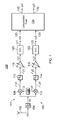
Figure 1 is a schematic illustration of a receiver according to an embodiment of the disclosure. -
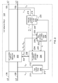
Figure 2 is a schematic illustration of a compensation stage of the receiver shown inFigure 1 . -
Figure 3 is a schematic illustration of a compensation coefficient application stage of the compensation stage shown inFigure 2 . - Referring to
Figure 1 , according to one embodiment of the disclosure there is provided areceiver 100. Thereceiver 100 is a Radio Frequency (RF)receiver 100 in the sense that it is arranged to receive an RF signal r'(t). Thereceiver 100 has anantenna 102 at which the RF signal r'(t) is received. Afilter 104, which is usually a band pass filter, is coupled to theantenna 102 and arranged to filter the RF signal r'(t) received at theantenna 102 to output a filtered RF signal r(t). - The
receiver 100 has an In-phase path (I-path) 101 and a Quadrature path (Q-path) 103. More specifically, thereceiver 100 has a local oscillator (LO)generator 106 for generating an I-path LO signal ν I (t) and a Q-path LO signal ν Q (t). The I-path LO signal ν I (t) and the Q-path LO signal ν Q (t) have the same LO frequency, but the phase of the Q-path LO signal ν Q (t) is shifted by 90° with respect to the phase of the I-path LO signal ν I (t). An I-path multiplier 108 multiplies the filtered RF signal r(t) with the I-path LO signal ν I (t) to output an I-path signal
path multiplier 110 multiplies the filtered RF signal r(t) with the Q-path LO signal ν Q (t) to output a Q-path signal


receiver 100 is of a type known as a Zero Intermediate Frequency (Zero-IF) receiver. However, the disclosure is equally applicable to embodiments in which the LO frequency is slightly lower than the carrier frequency of the received RF signal r'(t), meaning that the I-path signal

receiver 100 is of a type known as a Low Intermediate Frequency (Low-IF) receiver. - In the I-
path 101, an I-path filter 112 is coupled to an output of the I-path multiplier 108 and arranged to filter the I-path signal

path amplifier 116 is coupled to an output of the I-path filter 112 and arranged to amplify the filtered I-path signal

path amplifier 116 to convert the amplified I-path signal
path 103, a Q-path filter 114 is coupled to an output of the Q-path multiplier 110 and arranged to filter the Q-path signal

path amplifier 118 is coupled to an output of the Q-path filter 114 and arranged to amplify the filtered Q-path signal

path ADC 122 is coupled to an output of the Q-path amplifier 118 to convert the amplified Q-path signal
path filter 112 and the Q-path filter 114 are low pass filters. - Due to inevitable imperfections in the structure of the
receiver 100, it is difficult to ensure that the phase of the Q-path LO signal ν Q (t) is shifted with respect to the phase of the I-path LO signal ν I (t) by exactly 90°, leading to the digital Q-path signal xQ (t) having an error component. The inaccuracy of the phase shift can be defined as a phase error φ in the Q-path LO signal ν Q (t) with respect to the I-path LO signal ν I (t) shifted by exactly 90°. It is similarly difficult to ensure that the gain applied along the I-path 101 and the gain applied along the Q-path 103 are the same. This results in a gain error g in the form of a ratio of the gain of the Q-path 103 to the gain of the I-path 101. In anideal receiver 100, the phase error φ is zero, i.e. φ = 0 , and the gain error g is unity, i.e. g = 1, but in areal receiver 100 this does not hold true. - In this embodiment, the I-
path amplifier 116 and the Q-path amplifier 118 have variable gain, with the gain of theamplifiers receiver 100 to handle variations in the strength of the received RF signal r'(t), as well as changes in noise and interference. However, the variable gain of theamplifiers path amplifier 116 and the Q-path amplifier 118 are each implemented as two or more amplifiers with fixed gain that can be selectively coupled in I-path or Q-path respectively to provide a variable cumulative gain, coupling and decoupling one or more of the fixed gain amplifiers can cause step changes in the gain error g. - In order to deal with the gain error g and the phase error φ in the digital I-path signal xI (t) and the digital Q-path signal xQ (t), the
receiver 100 includes acompensation stage 124. The compensation stage is arranged to compensate for the gain error g and the phase error φ. Afirst input 126 of thecompensation stage 124 is coupled to anoutput 121 of the I-path ADC 120 so as to receive the digital I-path signal xI (t), and asecond input 128 of thecompensation stage 124 is coupled to anoutput 123 of the Q-path ADC 122 so as to receive the digital Q-path signal xQ (t). Thecompensation stage 124 delivers a compensated digital I-path signal yI (t) at afirst output 130 and a compensated digital Q-path signal yQ (t) at asecond output 132. - Referring to
Figure 2 , thecompensation stage 124 has a compensationcoefficient generation stage 200, a compensationcoefficient application stage 202, again control stage 208, a relativegradient generation stage 214 and a stepparameter generation stage 224. - The compensation
coefficient generation stage 200 is arranged to generate a first compensation coefficient W 1,1, a second compensation coefficient W 1,2, a third compensation coefficient W 2,1 and a fourth compensation coefficient W 2,2, and to deliver them to theoutput 206. Aninput 204 of the compensationcoefficient application stage 202 is coupled to anoutput 206 of the compensationcoefficient generation stage 200 so as to receive the first, second, third and fourth compensation coefficients W 1,1, W 1,2, W 2,1, W 2,2 from the compensationcoefficient generation stage 200. The compensationcoefficient application stage 202 is arranged to apply the first, second, third and fourth compensation coefficients W 1,1, W 1,2, W 2,1, W 2,2 to the digital I-path signal xI (t) and the digital Q-path signal xQ (t) to deliver the compensated digital I-path signal yI (t) and the compensated digital Q-path signal YQ (t). - Referring to
Figure 3 , in more detail, the compensationcoefficient application stage 202 has afirst multiplier 302 for multiplying the digital I-path signal xI (t) by the first compensation coefficient W 1,1 to generate a first signal y 1,1(t); asecond multiplier 304 for multiplying the digital Q-path signal xQ (t) by the second compensation coefficient W 1,2 to generate a second signal y 1,2(t); athird multiplier 306 for multiplying the digital I-path signal xI (t) by the third compensation coefficient W 2,1 to generate a third signal y 2,1(t); and afourth multiplier 308 for multiplying the digital Q-path signal xQ (t) by the fourth compensation coefficient W 2,2 to generate a fourth signal y 2,2(t). Thecoefficient application stage 202 also has a first summingstage 310 for summing the first signal y 1,1(t) and the second signal y 1,2(t) to generate the compensated digital I-path signal yI (t), and a second summingstage 312 for summing the third signal y 2,1 (t) and the fourth signal y 2,2(t) to generate the compensated digital Q-path signal yQ (t). This can be expressed mathematically as
- The
gain control stage 208 of thecompensation stage 124 has afirst input 210 arranged receive the digital I-path signal xI (t) and asecond input 212 arranged to receive the digital Q-path signal xQ (t). Thegain control stage 214 uses a level X 1,n of the digital I-path signal xI (t) at a time n and a level X 2,n of the digital Q-path signal xQ (t) at the time n to determine a gain control parameter cn, and deliver it to anoutput 213. - The relative
gradient generation stage 214 has afirst input 216 arranged to receive the compensated digital I-path signal yI (t), asecond input 218 arranged to receive the compensated digital Q-path signal yQ (t), and athird input 220 coupled to theoutput 213 of thegain control stage 208 so as to receive the gain control parameter cn . The relativegradient generation stage 214 uses a level Y 1,n of the compensated digital I-path signal yI (t) at the time n, a level Y 2,n of the compensated digital Q-path signal yQ (t) at the time n, and the gain control parameter Cn to determine first, second and fourth relative gradient coefficients H 1,1, H 1,2, H 2,2, and to deliver them to anoutput 223. - The step
parameter generation stage 224 has afirst input 226 coupled to theoutput 223 of the relativegradient generation stage 214 so as to receive the first, second and fourth relative gradient coefficients H 1,1, H 2,2, H 2,2 and asecond input 228 coupled to theoutput 206 of the compensationcoefficient generation stage 200 so as to receive the first, second, third and fourth compensation coefficients W 1,1, W 1,2, W 2,1, W 2,2, The stepfunction generation stage 224 determines a step parameter µ n for the time n using the first, second and fourth relative gradient coefficients H 1,1, H 1,2, H 2,2, the first, second, third and fourth compensation coefficients W 1,1, W 1,2 , W 2,1, W 2,2 and a step parameter µ n-1 determined for the preceding time n-1 and delivers the step parameter µ n determined for the time n to anoutput 232. - The compensation
coefficient generation stage 200 has afirst input 234 coupled to theoutput 223 of the relativegradient generation stage 214 so as to receive the first, second and fourth relative gradient coefficients H 1,1, H 1,2, H 2,2 and asecond input 236 coupled to theoutput 232 of the stepparameter generation stage 224 so as to receive the step parameter µ n . The compensationcoefficient generation stage 200 is arranged to generate the first, second, third and fourth compensation coefficients W 1,1, W 1,2, W 2,1, W 2,2 for the time n based on the first, second, third and fourth compensation coefficients W 1,1, W 1,2, W 2,1, W 2,2 for the preceding time n-1, the first, second and fourth relative gradient coefficients H 1,1, H 1,2, H 2,2 and the step parameter µ n . - In order to explain the operation of the
compensation stage 124, it is useful to define an ideal digital I-path signal zi (t) and an ideal digital Q-path signal zQ (t) when the phase error φ and the gain error g are perfectly compensated for by thecompensation stage 124. The relationship between the actual digital I-path and Q-path signals xI (t), xQ (t) of thereceiver 100 and the ideal digital I-path and Q-path signals zI (t), zQ (t) can be expressed as
- It is evident from equation (2) that the phase error φ and/or the gain error g having non-ideal values causes a component of the ideal digital I-path signal zI (t) to be present in the real digital Q-path signal xQ (t). Moreover, the ideal digital I-path signal zI (t) and the ideal digital Q-path signal zQ (t) are orthogonal to one another, and the unwanted components in the real digital Q-path signal xQ (t) comprise an undesired correlation between these signals.
- The compensated digital I-path signal yI (t) at the
first output 130 of thecompensation stage 124 and the compensated digital Q-path signal yQ (t) at thesecond output 132 of thecompensation stage 124 are estimates of the ideal digital I-path signal zI (t) and the ideal digital Q-path signal zQ (t). The purpose of thecompensation stage 124 is to ensure that the compensated digital I-path signal yI (t) and the compensated digital Q-path signal yQ (t) are the best possible estimates of the ideal digital I-path signal zI (t) and the ideal digital Q-path signal zQ (t). - Defining an uncompensated signal matrix Xn for a time n, in the form

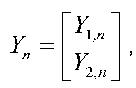

where W n-1 is a compensation matrix of the first, second, third and fourth compensation coefficients W 1,1, W 1,2, W 2,1 and W 2,2, in the form
coefficient generation stage 200 for a preceding time n-1. Moreover, by defining a relative gradient matrix Hn , in the form
coefficient generation stage 200 can be defined as
where I 2 is the identity matrix of size two by two. In other words, the step parameter µ n-1 for the preceding time n-1 and the relative gradient matrix Hn are used to update the compensation matrix Wn. - The relative
gradient generation stage 214 generates the relative gradient matrix Hn for the time n using
- It can be seen that the relative gradient matrix Hn depends on the compensated signal matrix Yn, but not on the uncompensated signal matrix Xn or, indeed, information about the ideal digital I-path and Q-path signals zI (t), zQ (t). Moreover, because the relative gradient matrix Hn is based on a multiplication of the compensated signal matrix Yn with its transpose

- The relative gradient matrix Hn is diagonally symmetric, which means that the second relative gradient coefficient H 1,2 is equal to a third relative gradient coefficient H 2,1, i.e. H 1,2 = H 2,1, and these coefficients can be determined in a single operation. Generation of the relative gradient matrix Hn by the relative
gradient generation stage 214 can therefore be expressed more specifically as
- The step
parameter generation stage 224 generates the step parameter µ n using
where α is a first constant, in this embodiment having a value of 997 thousandths, i.e. α = 0.997 , β is a second constant, in this embodiment having a value of two to the power of minus twenty three, i.e. β = 2-23, and Gn is an update function matrix of first, second, third and fourth update function parameters G 1,1, G 1,2, G 2,1 and G 2,2 in the form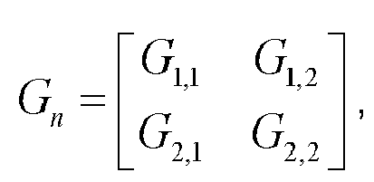

- The update function matrix Gn is an expression of the rate of change of the compensation matrix Wn with the step parameter µ n . By incorporating the update function matrix Gn in the generation of the step parameter µ n based on equation (6), the step parameter µ n is made adaptive. Specifically, variations in the rate of change of the compensation matrix Wn with the step parameter µ n cause the magnitude of the step parameter µ n to change.
- The structure of equation (7), by which the step parameter µ n-1, adjusted using the second constant β and the trace function, is subtracted from the same step parameter µ n-1 adjusted using the first constant α, provides a forgetting factor to smooth changes in the value of the step parameter µ n .
- Although the first constant α is described as having a value of 997 thousandths, i.e. α = 0.997 , and the second constant β is described as having a value of two to the power of minus twenty three, i.e. β = 2-23, these values are not essential. Rather, the values can be optimised for a particular implementation. Typically, in most implementations, the first constant α has a value of in the order of thousandths less than 1, and the second constant β has a value between two to the power of minus twenty to two to the power of minus twenty five.
- In order to generate the step parameter µ n , the step
parameter generation stage 224 first determines the update function matrix Gn based on equation (8). In order to do this, it is useful to define, as a intermediate step, an update matrix Upn, in the form

- This allows the update function matrix Gn determined by the step
parameter generation stage 224 to be expressed more specifically as
- With the first, second, third and fourth update function parameters G 1,1, G 1,2, G 2,1 and G 2,2 determined, the step
parameter generation stage 224 determines the step parameter µ n based on equation (7). Generation of the step parameter µ n by the stepparameter generation stage 224 can be expressed more specifically as
- The compensation
coefficient generation stage 200 uses the step parameter µ n and the first, second and fourth relative gradient coefficients H 1,1, H 1,2, H 2,2 to generate the first, second, third and fourth compensation coefficients W 1,1, W 1,2, W 2,1, W 2,2 based on equation (4). Again, it is useful to perform this generation using an intermediate step based on the first, second, third and fourth update coefficients Up 1,1, Up 1,2 , Up 2,1, Up 2,2 of the update matrix Upn, so that
- In this embodiment, the gain control parameter cn for time n is generated by the
gain control stage 208 using
where a first gain control value an at time n is defined by
and a second gain control value bn at time n is defined by
where ∥∥ denotes a norm and λ is a smoothing factor, which in this embodiment is equal to one ten thousandth, i.e. λ = 0.0001. By referring to the levels X 1,n , X 2,n of the digital I-path signal xI (t) and the digital Q-path signal xQ (t) instead of the uncompensated signal matrix Xn , determination of the first gain control value an can be expressed more specifically as
- In order to determine the gain control parameter cn , the
gain control stage 208 determines the first gain control value an at the time n using equation (14) or (16). With the first gain control value an at the time n determined, thegain control stage 208 determines the second gain control value bn and the gain control parameter cn , using equations (13) and (15). For simplicity, the log2 operation in equation (15) is simplified by finding the power of two closest to the gain control value an , rather than performing the log2 operation in full. Also, the operation defined in equation (13) is implemented as a right shift by a number of bits equal to the second gain control value bn . Once determined, the gain control parameter cn is delivered tooutput 213 of thegain control stage 208. - As the level of first gain control value an at the time n depends on the level of the first gain control value a n-1 at the preceding time n-1, the level is determined iteratively. Moreover, on start-up of the process, it can take a number of iterations for an accurate level to be arrived at. For this reason, when the
compensation stage 124 begins operation, thegain control stage 208 is run for a period of time N before compensation of the digital I-path signal xI (t) and the digital Q-path signal xQ (t) begins. At the beginning of this period of time, thegain control stage 208 sets the first gain control value a n-1 at zero, i.e. a n-1 = 0. Optionally, the smoothing factor λ is also set at a different, higher value. In this embodiment, the smoothing factor λ is set at three tenths, i.e. λ = 0.3. During the period of time N, the compensation matrix Wn, the update function matrix Gn and the step parameter µ n are held constant. In this embodiment, the constant compensation matrix Wn , update function matrix Gn and step parameter µ n are
- Although the smoothing factor λ is described as having an initial value of 0.3 and a normal value of one ten thousandth, these values are not essential. Rather, the values can be optimised for a particular implementation. Typically, in most implementations, the smoothing factor λ has an initial value in the order of tenths, and a normal value in the order of ten thousandths. Similarly, the constant value of the step parameter µ-1 used during start up need not be 2-6. Rather, it is typically of the order of millionths.
- In another embodiment, the gain control parameter cn is determined as the inverse of the first gain control value an .
- In yet another embodiment, the step function µ n given in equation (7) above is replaced by

where
- In this embodiment, the first constant α has a value of one ten thousandth, i.e. α = 10-4 and the second constant β has a value of one hundredth, i.e. β = 10-2, and a third constant γ has a value of 95 hundredths, i.e. γ = 0.95. However, as before, these values are not essential, and the first constant cf typically has a value in the order of ten thoursandths, the second constant β has a value in the order of hundredths, and the third constant γ has a value of hundredths less than one.
- Updating the step function µ n using equations (18) and (19) instead of equation (7) provides different convergence properties. In particular, the compensation coefficients W 1,1, W 1,2, W 2,1, W 2,2 tend to converge more quickly, but are slightly less stable during periods when the phase error φ and gain error g do not change significantly.
- Other variations and modifications will be apparent to the skilled person. Such variations and modifications may involve equivalent and other features that are already known and which may be used instead of, or in addition to, features described herein. Features that are described in the context of separate embodiments may be provided in combination in a single embodiment. Conversely, features that are described in the context of a single embodiment may also be provided separately or in any suitable subcombination.
- It should be noted that the term "comprising" does not exclude other elements or steps, the term "a" or "an" does not exclude a plurality, a single feature may fulfil the functions of several features recited in the claims and reference signs in the claims shall not be construed as limiting the scope of the claims. It should also be noted that the Figures are not necessarily to scale; emphasis instead generally being placed upon illustrating the principles of the present invention.
Claims (15)
- A receiver (100) for receiving a signal, the receiver (100) comprising:a local oscillator (106) arranged to deliver an in-phase local oscillator signal and a quadrature local oscillator signal;an in-phase signal path (101) having a mixer (108) arranged to mix the signal received by the receiver (100) with the in-phase local oscillator signal to deliver an in-phase signal, and an analogue-to-digital converter (120) arranged convert the in-phase signal to a digital in-phase signal; anda quadrature signal path (103) having a mixer (110) arranged to mix the signal received by the receiver (100) with the quadrature local oscillator signal to deliver a quadrature signal, and an analogue-to-digital converter (122) arranged convert the quadrature signal to a digital quadrature signal;a compensation stage (124) arranged deliver a compensated digital in-phase signal and a compensated digital quadrature signal by applying compensation coefficients to the digital in-phase signal and the digital quadrature signal; anda compensation coefficient generator (200) arranged to generate the compensation coefficients by iteratively updating them using a relative gradient of the compensated digital in-phase signal and the compensated digital quadrature signal, and a step parameter,wherein the compensation stage (124) is arranged to adjust the magnitude of the step parameter based on the rate of change of the compensation coefficients.
- The receiver (100) of claim 1, wherein the compensation stage (124) is arranged to adjust the magnitude of the step parameter based on the rate of change of the compensation coefficients with the magnitude of the step parameter.
- The receiver (100) of claim 1 or claim 2, wherein the compensation stage (124) is arranged to adjust the magnitude of the step parameter based on the relative gradient of the compensated digital in-phase signal and the compensated digital quadrature signal.
- The receiver (100) of claim 1, wherein the compensation stage (124) is arranged to adjust the magnitude of the step parameter based on a trace function of a first matrix of the rate of change of the compensation coefficients with the magnitude of the step parameter and a second matrix of the relative gradient of the compensated digital in-phase signal and the compensated digital quadrature signal.
- The receiver (100) of claim 4, wherein the compensation stage (124) is arranged to adjust the magnitude of the step parameter based on

where µ n-1 is the magnitude of the step parameter, µ n is the adjusted magnitude of the step parameter, Gn is the first matrix, Hn is the second matrix and α and β are constants. - The receiver (100) of claim 4, wherein the compensation stage (124) is arranged to adjust the magnitude of the step parameter based on

where
µ n-1 is the magnitude of the step parameter, µ n is the adjusted magnitude of the step parameter, Gn is the first matrix, Hn is the second matrix and α, β and γ are constants. - The receiver (100) of any one of the preceding claims, further comprising a gain controller (208) arranged to generate a gain control parameter and a relative gradient generation stage (214) arranged to generate the relative gradient based on the gain control parameter, the compensated digital in-phase signal and the compensated digital quadrature signal.
- The receiver (100) of claim 7, wherein the relative gradient generation stage (214) is arranged to generate the relative gradient based on

where Hn is a relative gradient matrix, cn is the gain control parameter, Yn is a matrix of the compensated digital in-phase signal and the compensated digital quadrature signal at a time n,
- The receiver (100) of claim 7 or claim 8, wherein the gain controller (208) is arranged to generate the gain control parameter based on the uncompensated digital in-phase signal and the uncompensated digital quadrature signal.
- The receiver (100) of any one of claims 7 to 9, wherein the gain control parameter has a value that normalises the compensated digital in-phase signal and the compensated digital quadrature signal.
- The receiver (100) of any one of claims 7 to 10, wherein the gain controller (208) is arranged to generate the gain control parameter based on

where bn is a gain control value defined by

where Xn is a matrix of the uncompensated digital in-phase signal and the uncompensated digital quadrature signal at time n, ∥∥ denotes a norm and λ is a smoothing factor. - The receiver (100) of any one of the preceding claims, wherein the compensation coefficients generated by the compensation coefficient generator (200) comprise a first compensation coefficient, a second compensation coefficient, a third compensation coefficient and a fourth compensation coefficient, and the compensation stage (124) is arranged to generate a first signal and a third signal by multiplying the digital in-phase signal with the first compensation coefficient and the third compensation coefficient respectively, to generate a second signal and a fourth signal by multiplying the digital quadrature signal with the second compensation coefficient and the fourth compensation coefficient respectively, to sum the first signal and the second signal to output the compensated digital in-phase signal, and to sum the third signal and the fourth signal to output the compensated digital quadrature signal.
- A communication device incorporating the receiver of any one of the preceding claims.
- A method comprising:receiving a signal;delivering an in-phase local oscillator signal and a quadrature local oscillator signal;in an in-phase signal path (101), mixing the received signal with the in-phase local oscillator signal to deliver an in-phase signal and converting the in-phase signal to a digital in-phase signal; andin a quadrature signal path (103), mixing the received signal with the quadrature local oscillator signal to deliver a quadrature signal and converting the quadrature signal to a digital quadrature signal;applying compensation coefficients to the digital in-phase signal and the digital quadrature signal to deliver a compensated digital in-phase signal and a compensated digital quadrature signal;generating the compensation coefficients by iteratively updating them using a relative gradient of the compensated digital in-phase signal and the compensated digital quadrature signal, and a step parameter;and adjusting the magnitude of the step parameter based on the rate of change of the compensation coefficients.
- A computer readable medium carrying computer programme code arranged to carry out the method of claim 11 when executed by a processor.
Priority Applications (3)
| Application Number | Priority Date | Filing Date | Title |
|---|---|---|---|
| EP12163662.5A EP2651087B1 (en) | 2012-04-10 | 2012-04-10 | IQ mismatch compensation |
| US14/390,507 US9203666B2 (en) | 2012-04-10 | 2013-04-10 | IQ mismatch compensation |
| PCT/EP2013/057445 WO2013153087A1 (en) | 2012-04-10 | 2013-04-10 | Iq mismatch compensation |
Applications Claiming Priority (1)
| Application Number | Priority Date | Filing Date | Title |
|---|---|---|---|
| EP12163662.5A EP2651087B1 (en) | 2012-04-10 | 2012-04-10 | IQ mismatch compensation |
Publications (2)
| Publication Number | Publication Date |
|---|---|
| EP2651087A1 true EP2651087A1 (en) | 2013-10-16 |
| EP2651087B1 EP2651087B1 (en) | 2016-07-20 |
Family
ID=46000850
Family Applications (1)
| Application Number | Title | Priority Date | Filing Date |
|---|---|---|---|
| EP12163662.5A Not-in-force EP2651087B1 (en) | 2012-04-10 | 2012-04-10 | IQ mismatch compensation |
Country Status (3)
| Country | Link |
|---|---|
| US (1) | US9203666B2 (en) |
| EP (1) | EP2651087B1 (en) |
| WO (1) | WO2013153087A1 (en) |
Cited By (2)
| Publication number | Priority date | Publication date | Assignee | Title |
|---|---|---|---|---|
| CN111211797A (en) * | 2020-01-14 | 2020-05-29 | 安徽大学 | Receiver compensation method and compensation system and electronic device thereof |
| CN114124640A (en) * | 2020-08-31 | 2022-03-01 | 中兴通讯股份有限公司 | Signal compensation processing method and device |
Families Citing this family (5)
| Publication number | Priority date | Publication date | Assignee | Title |
|---|---|---|---|---|
| KR102055192B1 (en) * | 2017-08-25 | 2019-12-12 | 한밭대학교 산학협력단 | Apparatus and method for calibrating i/q imbalance of direct-conversion transmitter |
| JP2019054497A (en) * | 2017-09-19 | 2019-04-04 | 東芝メモリ株式会社 | Reception device, transmission device, and communication system |
| US10749555B2 (en) | 2018-09-26 | 2020-08-18 | Samsung Electronics Co., Ltd. | Time-domain IQ mismatch compensator with frequency-domain observations |
| CN113055032B (en) * | 2019-12-27 | 2022-07-19 | 珠海全志科技股份有限公司 | Method and device for acquiring compensation values of IQ mismatch and carrier leakage and computer equipment |
| CN119449540B (en) * | 2024-11-05 | 2025-10-24 | 深圳市联洲国际技术有限公司 | Signal determination method, device, storage medium and processor for receiver |
Citations (3)
| Publication number | Priority date | Publication date | Assignee | Title |
|---|---|---|---|---|
| US20020097812A1 (en) * | 2000-12-01 | 2002-07-25 | John Wiss | In-phase and quadrature-phase rebalancer |
| US20090147886A1 (en) * | 2007-12-06 | 2009-06-11 | Cambridge Silicon Radio Limited | Adaptive IQ Alignment Apparatus |
| US20110182388A1 (en) * | 2010-01-28 | 2011-07-28 | Korea Advanced Institute Of Science And Technology | Apparatus for rejecting image in receiver |
Family Cites Families (7)
| Publication number | Priority date | Publication date | Assignee | Title |
|---|---|---|---|---|
| US5705949A (en) * | 1996-09-13 | 1998-01-06 | U.S. Robotics Access Corp. | Compensation method for I/Q channel imbalance errors |
| EP1168597A1 (en) * | 2000-06-23 | 2002-01-02 | NTT DoCoMo, Inc. | Quadrature Receiver with Orthogonality Correction |
| US7876856B2 (en) * | 2005-06-23 | 2011-01-25 | Texas Instrumentals Incorporated | Quadrature receiver with correction engine, coefficient controller and adaptation engine |
| US7593484B2 (en) * | 2005-09-30 | 2009-09-22 | Skyworks Solutions, Inc. | Radio frequency (RF) receiver with double loop integrated fast response automatic gain control (AGC) |
| US8064542B1 (en) * | 2006-03-16 | 2011-11-22 | Marvell International Ltd. | Systems and methods for I/Q imbalance correction and calibration of variable modulus signals |
| US8654885B2 (en) * | 2006-06-06 | 2014-02-18 | Qualcomm Incorporated | Fast in-phase and quadrature imbalance calibration |
| US8644522B2 (en) * | 2011-03-31 | 2014-02-04 | Broadcom Corporation | Method and system for modeling external volume changes within an acoustic echo canceller |
-
2012
- 2012-04-10 EP EP12163662.5A patent/EP2651087B1/en not_active Not-in-force
-
2013
- 2013-04-10 US US14/390,507 patent/US9203666B2/en not_active Expired - Fee Related
- 2013-04-10 WO PCT/EP2013/057445 patent/WO2013153087A1/en not_active Ceased
Patent Citations (3)
| Publication number | Priority date | Publication date | Assignee | Title |
|---|---|---|---|---|
| US20020097812A1 (en) * | 2000-12-01 | 2002-07-25 | John Wiss | In-phase and quadrature-phase rebalancer |
| US20090147886A1 (en) * | 2007-12-06 | 2009-06-11 | Cambridge Silicon Radio Limited | Adaptive IQ Alignment Apparatus |
| US20110182388A1 (en) * | 2010-01-28 | 2011-07-28 | Korea Advanced Institute Of Science And Technology | Apparatus for rejecting image in receiver |
Non-Patent Citations (1)
| Title |
|---|
| VALKAMA ET AL.: "Blind I/Q Signal Separation-Based Solutions for Receiver Signal Processing", EURASIP JOURNAL ON APPLIED SIGNAL PROCESSING, 1 January 2005 (2005-01-01), pages 2708 - 2718 |
Cited By (2)
| Publication number | Priority date | Publication date | Assignee | Title |
|---|---|---|---|---|
| CN111211797A (en) * | 2020-01-14 | 2020-05-29 | 安徽大学 | Receiver compensation method and compensation system and electronic device thereof |
| CN114124640A (en) * | 2020-08-31 | 2022-03-01 | 中兴通讯股份有限公司 | Signal compensation processing method and device |
Also Published As
| Publication number | Publication date |
|---|---|
| EP2651087B1 (en) | 2016-07-20 |
| US20150172082A1 (en) | 2015-06-18 |
| US9203666B2 (en) | 2015-12-01 |
| WO2013153087A1 (en) | 2013-10-17 |
Similar Documents
| Publication | Publication Date | Title |
|---|---|---|
| US9203666B2 (en) | IQ mismatch compensation | |
| EP2894823B1 (en) | Coefficient estimation for digital IQ calibration | |
| EP2060081B1 (en) | Frequency dependent I/Q imbalance estimation | |
| EP1514393B1 (en) | Amplitude imbalance compensation of quadrature modulator | |
| US7061994B2 (en) | Methods and apparatus for I/Q imbalance compensation | |
| EP2181533B1 (en) | IQ imbalance image suppression in presence of unknown phase shift | |
| US20030231723A1 (en) | Digital estimation and correction of I/Q mismatch in direct conversion receivers | |
| US9680674B2 (en) | I/Q calibration techniques | |
| CN100542154C (en) | Direct Conversion Receiver Calibrating Phase and Gain Mismatches | |
| US9749172B2 (en) | Calibration method and calibration apparatus for calibrating mismatch between first signal path and second signal path of transmitter/receiver | |
| US8976914B2 (en) | Multi-tap IQ imbalance estimation and correction circuit and method | |
| US8363712B2 (en) | Apparatus and method for adaptive I/Q imbalance compensation | |
| US11626897B2 (en) | Transmitter circuit, compensation value calibration device and method for calibrating IQ imbalance compensation values | |
| US8681896B1 (en) | Transmitter I/Q and carrier leak calibration | |
| US20090122918A1 (en) | Methods for Compensating for I/Q Imbalance in OFDM Systems | |
| EP1916764B1 (en) | Method and apparatus for compensating for mismatch occurring in radio frequency quadrature transceiver | |
| JP2019057878A (en) | Carrier leak compensation method in orthogonal modulator | |
| EP1435687B1 (en) | Direct conversion receiver | |
| JP2009527968A (en) | In-phase and quadrature path imbalance compensation | |
| US7672655B1 (en) | Frequency-selective and adaptive I/Q mismatch digital compensation | |
| US9647867B2 (en) | Wideband IQ mismatch correction for direct down-conversion receiver | |
| US8218683B2 (en) | Method for compensation for any phase and/or amplitude error in a receiver | |
| US9020026B2 (en) | Frequency dependent I/Q imbalance compensation | |
| EP3028428B1 (en) | Direct conversion receiver device with first and second stages and related methods | |
| WO2012094087A1 (en) | Apparatus and method for adaptive i/q imbalance compensation |
Legal Events
| Date | Code | Title | Description |
|---|---|---|---|
| PUAI | Public reference made under article 153(3) epc to a published international application that has entered the european phase |
Free format text: ORIGINAL CODE: 0009012 |
|
| AK | Designated contracting states |
Kind code of ref document: A1 Designated state(s): AL AT BE BG CH CY CZ DE DK EE ES FI FR GB GR HR HU IE IS IT LI LT LU LV MC MK MT NL NO PL PT RO RS SE SI SK SM TR |
|
| AX | Request for extension of the european patent |
Extension state: BA ME |
|
| 17P | Request for examination filed |
Effective date: 20140416 |
|
| RBV | Designated contracting states (corrected) |
Designated state(s): AL AT BE BG CH CY CZ DE DK EE ES FI FR GB GR HR HU IE IS IT LI LT LU LV MC MK MT NL NO PL PT RO RS SE SI SK SM TR |
|
| 17Q | First examination report despatched |
Effective date: 20150610 |
|
| GRAP | Despatch of communication of intention to grant a patent |
Free format text: ORIGINAL CODE: EPIDOSNIGR1 |
|
| INTG | Intention to grant announced |
Effective date: 20151016 |
|
| GRAP | Despatch of communication of intention to grant a patent |
Free format text: ORIGINAL CODE: EPIDOSNIGR1 |
|
| INTG | Intention to grant announced |
Effective date: 20160314 |
|
| GRAS | Grant fee paid |
Free format text: ORIGINAL CODE: EPIDOSNIGR3 |
|
| GRAA | (expected) grant |
Free format text: ORIGINAL CODE: 0009210 |
|
| AK | Designated contracting states |
Kind code of ref document: B1 Designated state(s): AL AT BE BG CH CY CZ DE DK EE ES FI FR GB GR HR HU IE IS IT LI LT LU LV MC MK MT NL NO PL PT RO RS SE SI SK SM TR |
|
| REG | Reference to a national code |
Ref country code: GB Ref legal event code: FG4D |
|
| REG | Reference to a national code |
Ref country code: CH Ref legal event code: EP |
|
| REG | Reference to a national code |
Ref country code: IE Ref legal event code: FG4D |
|
| REG | Reference to a national code |
Ref country code: AT Ref legal event code: REF Ref document number: 814869 Country of ref document: AT Kind code of ref document: T Effective date: 20160815 |
|
| REG | Reference to a national code |
Ref country code: DE Ref legal event code: R096 Ref document number: 602012020618 Country of ref document: DE |
|
| REG | Reference to a national code |
Ref country code: LT Ref legal event code: MG4D |
|
| REG | Reference to a national code |
Ref country code: NL Ref legal event code: MP Effective date: 20160720 |
|
| REG | Reference to a national code |
Ref country code: AT Ref legal event code: MK05 Ref document number: 814869 Country of ref document: AT Kind code of ref document: T Effective date: 20160720 |
|
| REG | Reference to a national code |
Ref country code: DE Ref legal event code: R082 Ref document number: 602012020618 Country of ref document: DE Representative=s name: GRUENECKER PATENT- UND RECHTSANWAELTE PARTG MB, DE Ref country code: DE Ref legal event code: R081 Ref document number: 602012020618 Country of ref document: DE Owner name: OCT CIRCUIT TECHNOLOGIES INTERNATIONAL LTD., IE Free format text: FORMER OWNER: ST-ERICSSON SA, PLAN-LES-OUATES, CH |
|
| RAP2 | Party data changed (patent owner data changed or rights of a patent transferred) |
Owner name: OCT CIRCUIT TECHNOLOGIES INTERNATIONAL LIMITED |
|
| PG25 | Lapsed in a contracting state [announced via postgrant information from national office to epo] |
Ref country code: NL Free format text: LAPSE BECAUSE OF FAILURE TO SUBMIT A TRANSLATION OF THE DESCRIPTION OR TO PAY THE FEE WITHIN THE PRESCRIBED TIME-LIMIT Effective date: 20160720 Ref country code: FI Free format text: LAPSE BECAUSE OF FAILURE TO SUBMIT A TRANSLATION OF THE DESCRIPTION OR TO PAY THE FEE WITHIN THE PRESCRIBED TIME-LIMIT Effective date: 20160720 Ref country code: IT Free format text: LAPSE BECAUSE OF FAILURE TO SUBMIT A TRANSLATION OF THE DESCRIPTION OR TO PAY THE FEE WITHIN THE PRESCRIBED TIME-LIMIT Effective date: 20160720 Ref country code: HR Free format text: LAPSE BECAUSE OF FAILURE TO SUBMIT A TRANSLATION OF THE DESCRIPTION OR TO PAY THE FEE WITHIN THE PRESCRIBED TIME-LIMIT Effective date: 20160720 Ref country code: LT Free format text: LAPSE BECAUSE OF FAILURE TO SUBMIT A TRANSLATION OF THE DESCRIPTION OR TO PAY THE FEE WITHIN THE PRESCRIBED TIME-LIMIT Effective date: 20160720 Ref country code: IS Free format text: LAPSE BECAUSE OF FAILURE TO SUBMIT A TRANSLATION OF THE DESCRIPTION OR TO PAY THE FEE WITHIN THE PRESCRIBED TIME-LIMIT Effective date: 20161120 Ref country code: NO Free format text: LAPSE BECAUSE OF FAILURE TO SUBMIT A TRANSLATION OF THE DESCRIPTION OR TO PAY THE FEE WITHIN THE PRESCRIBED TIME-LIMIT Effective date: 20161020 Ref country code: RS Free format text: LAPSE BECAUSE OF FAILURE TO SUBMIT A TRANSLATION OF THE DESCRIPTION OR TO PAY THE FEE WITHIN THE PRESCRIBED TIME-LIMIT Effective date: 20160720 |
|
| PG25 | Lapsed in a contracting state [announced via postgrant information from national office to epo] |
Ref country code: ES Free format text: LAPSE BECAUSE OF FAILURE TO SUBMIT A TRANSLATION OF THE DESCRIPTION OR TO PAY THE FEE WITHIN THE PRESCRIBED TIME-LIMIT Effective date: 20160720 Ref country code: BE Free format text: LAPSE BECAUSE OF FAILURE TO SUBMIT A TRANSLATION OF THE DESCRIPTION OR TO PAY THE FEE WITHIN THE PRESCRIBED TIME-LIMIT Effective date: 20160720 Ref country code: PT Free format text: LAPSE BECAUSE OF FAILURE TO SUBMIT A TRANSLATION OF THE DESCRIPTION OR TO PAY THE FEE WITHIN THE PRESCRIBED TIME-LIMIT Effective date: 20161121 Ref country code: GR Free format text: LAPSE BECAUSE OF FAILURE TO SUBMIT A TRANSLATION OF THE DESCRIPTION OR TO PAY THE FEE WITHIN THE PRESCRIBED TIME-LIMIT Effective date: 20161021 Ref country code: SE Free format text: LAPSE BECAUSE OF FAILURE TO SUBMIT A TRANSLATION OF THE DESCRIPTION OR TO PAY THE FEE WITHIN THE PRESCRIBED TIME-LIMIT Effective date: 20160720 Ref country code: PL Free format text: LAPSE BECAUSE OF FAILURE TO SUBMIT A TRANSLATION OF THE DESCRIPTION OR TO PAY THE FEE WITHIN THE PRESCRIBED TIME-LIMIT Effective date: 20160720 Ref country code: AT Free format text: LAPSE BECAUSE OF FAILURE TO SUBMIT A TRANSLATION OF THE DESCRIPTION OR TO PAY THE FEE WITHIN THE PRESCRIBED TIME-LIMIT Effective date: 20160720 Ref country code: LV Free format text: LAPSE BECAUSE OF FAILURE TO SUBMIT A TRANSLATION OF THE DESCRIPTION OR TO PAY THE FEE WITHIN THE PRESCRIBED TIME-LIMIT Effective date: 20160720 |
|
| REG | Reference to a national code |
Ref country code: FR Ref legal event code: PLFP Year of fee payment: 6 |
|
| REG | Reference to a national code |
Ref country code: DE Ref legal event code: R097 Ref document number: 602012020618 Country of ref document: DE |
|
| PG25 | Lapsed in a contracting state [announced via postgrant information from national office to epo] |
Ref country code: RO Free format text: LAPSE BECAUSE OF FAILURE TO SUBMIT A TRANSLATION OF THE DESCRIPTION OR TO PAY THE FEE WITHIN THE PRESCRIBED TIME-LIMIT Effective date: 20160720 Ref country code: EE Free format text: LAPSE BECAUSE OF FAILURE TO SUBMIT A TRANSLATION OF THE DESCRIPTION OR TO PAY THE FEE WITHIN THE PRESCRIBED TIME-LIMIT Effective date: 20160720 |
|
| PGFP | Annual fee paid to national office [announced via postgrant information from national office to epo] |
Ref country code: FR Payment date: 20170322 Year of fee payment: 6 |
|
| PLBE | No opposition filed within time limit |
Free format text: ORIGINAL CODE: 0009261 |
|
| STAA | Information on the status of an ep patent application or granted ep patent |
Free format text: STATUS: NO OPPOSITION FILED WITHIN TIME LIMIT |
|
| PG25 | Lapsed in a contracting state [announced via postgrant information from national office to epo] |
Ref country code: BG Free format text: LAPSE BECAUSE OF FAILURE TO SUBMIT A TRANSLATION OF THE DESCRIPTION OR TO PAY THE FEE WITHIN THE PRESCRIBED TIME-LIMIT Effective date: 20161020 Ref country code: SK Free format text: LAPSE BECAUSE OF FAILURE TO SUBMIT A TRANSLATION OF THE DESCRIPTION OR TO PAY THE FEE WITHIN THE PRESCRIBED TIME-LIMIT Effective date: 20160720 Ref country code: CZ Free format text: LAPSE BECAUSE OF FAILURE TO SUBMIT A TRANSLATION OF THE DESCRIPTION OR TO PAY THE FEE WITHIN THE PRESCRIBED TIME-LIMIT Effective date: 20160720 Ref country code: SM Free format text: LAPSE BECAUSE OF FAILURE TO SUBMIT A TRANSLATION OF THE DESCRIPTION OR TO PAY THE FEE WITHIN THE PRESCRIBED TIME-LIMIT Effective date: 20160720 Ref country code: DK Free format text: LAPSE BECAUSE OF FAILURE TO SUBMIT A TRANSLATION OF THE DESCRIPTION OR TO PAY THE FEE WITHIN THE PRESCRIBED TIME-LIMIT Effective date: 20160720 |
|
| PGFP | Annual fee paid to national office [announced via postgrant information from national office to epo] |
Ref country code: GB Payment date: 20170324 Year of fee payment: 6 |
|
| 26N | No opposition filed |
Effective date: 20170421 |
|
| PGFP | Annual fee paid to national office [announced via postgrant information from national office to epo] |
Ref country code: DE Payment date: 20170321 Year of fee payment: 6 |
|
| PG25 | Lapsed in a contracting state [announced via postgrant information from national office to epo] |
Ref country code: SI Free format text: LAPSE BECAUSE OF FAILURE TO SUBMIT A TRANSLATION OF THE DESCRIPTION OR TO PAY THE FEE WITHIN THE PRESCRIBED TIME-LIMIT Effective date: 20160720 |
|
| REG | Reference to a national code |
Ref country code: CH Ref legal event code: PL |
|
| REG | Reference to a national code |
Ref country code: IE Ref legal event code: MM4A |
|
| PG25 | Lapsed in a contracting state [announced via postgrant information from national office to epo] |
Ref country code: MC Free format text: LAPSE BECAUSE OF FAILURE TO SUBMIT A TRANSLATION OF THE DESCRIPTION OR TO PAY THE FEE WITHIN THE PRESCRIBED TIME-LIMIT Effective date: 20160720 |
|
| PG25 | Lapsed in a contracting state [announced via postgrant information from national office to epo] |
Ref country code: CH Free format text: LAPSE BECAUSE OF NON-PAYMENT OF DUE FEES Effective date: 20170430 Ref country code: LI Free format text: LAPSE BECAUSE OF NON-PAYMENT OF DUE FEES Effective date: 20170430 Ref country code: LU Free format text: LAPSE BECAUSE OF NON-PAYMENT OF DUE FEES Effective date: 20170410 |
|
| PG25 | Lapsed in a contracting state [announced via postgrant information from national office to epo] |
Ref country code: IE Free format text: LAPSE BECAUSE OF NON-PAYMENT OF DUE FEES Effective date: 20170410 |
|
| PG25 | Lapsed in a contracting state [announced via postgrant information from national office to epo] |
Ref country code: MT Free format text: LAPSE BECAUSE OF NON-PAYMENT OF DUE FEES Effective date: 20170410 |
|
| PG25 | Lapsed in a contracting state [announced via postgrant information from national office to epo] |
Ref country code: AL Free format text: LAPSE BECAUSE OF FAILURE TO SUBMIT A TRANSLATION OF THE DESCRIPTION OR TO PAY THE FEE WITHIN THE PRESCRIBED TIME-LIMIT Effective date: 20160720 |
|
| REG | Reference to a national code |
Ref country code: DE Ref legal event code: R119 Ref document number: 602012020618 Country of ref document: DE |
|
| GBPC | Gb: european patent ceased through non-payment of renewal fee |
Effective date: 20180410 |
|
| PG25 | Lapsed in a contracting state [announced via postgrant information from national office to epo] |
Ref country code: DE Free format text: LAPSE BECAUSE OF NON-PAYMENT OF DUE FEES Effective date: 20181101 |
|
| PG25 | Lapsed in a contracting state [announced via postgrant information from national office to epo] |
Ref country code: GB Free format text: LAPSE BECAUSE OF NON-PAYMENT OF DUE FEES Effective date: 20180410 |
|
| PG25 | Lapsed in a contracting state [announced via postgrant information from national office to epo] |
Ref country code: FR Free format text: LAPSE BECAUSE OF NON-PAYMENT OF DUE FEES Effective date: 20180430 |
|
| PG25 | Lapsed in a contracting state [announced via postgrant information from national office to epo] |
Ref country code: HU Free format text: LAPSE BECAUSE OF FAILURE TO SUBMIT A TRANSLATION OF THE DESCRIPTION OR TO PAY THE FEE WITHIN THE PRESCRIBED TIME-LIMIT; INVALID AB INITIO Effective date: 20120410 |
|
| PG25 | Lapsed in a contracting state [announced via postgrant information from national office to epo] |
Ref country code: CY Free format text: LAPSE BECAUSE OF NON-PAYMENT OF DUE FEES Effective date: 20160720 |
|
| PG25 | Lapsed in a contracting state [announced via postgrant information from national office to epo] |
Ref country code: MK Free format text: LAPSE BECAUSE OF FAILURE TO SUBMIT A TRANSLATION OF THE DESCRIPTION OR TO PAY THE FEE WITHIN THE PRESCRIBED TIME-LIMIT Effective date: 20160720 |
|
| PG25 | Lapsed in a contracting state [announced via postgrant information from national office to epo] |
Ref country code: TR Free format text: LAPSE BECAUSE OF FAILURE TO SUBMIT A TRANSLATION OF THE DESCRIPTION OR TO PAY THE FEE WITHIN THE PRESCRIBED TIME-LIMIT Effective date: 20160720 |