EP2649549B1 - Rf transistor packages with internal stability network including intra-capacitor resistors and methods of forming rf transistor packages with internal stability networks including intra-capacitor resistors - Google Patents
Rf transistor packages with internal stability network including intra-capacitor resistors and methods of forming rf transistor packages with internal stability networks including intra-capacitor resistors Download PDFInfo
- Publication number
- EP2649549B1 EP2649549B1 EP11847818.9A EP11847818A EP2649549B1 EP 2649549 B1 EP2649549 B1 EP 2649549B1 EP 11847818 A EP11847818 A EP 11847818A EP 2649549 B1 EP2649549 B1 EP 2649549B1
- Authority
- EP
- European Patent Office
- Prior art keywords
- input
- transistor
- capacitors
- terminals
- resistors
- Prior art date
- Legal status (The legal status is an assumption and is not a legal conclusion. Google has not performed a legal analysis and makes no representation as to the accuracy of the status listed.)
- Active
Links
Images





Classifications
-
- H—ELECTRICITY
- H10—SEMICONDUCTOR DEVICES; ELECTRIC SOLID-STATE DEVICES NOT OTHERWISE PROVIDED FOR
- H10W—GENERIC PACKAGES, INTERCONNECTIONS, CONNECTORS OR OTHER CONSTRUCTIONAL DETAILS OF DEVICES COVERED BY CLASS H10
- H10W44/00—Electrical arrangements for controlling or matching impedance
- H10W44/601—Capacitive arrangements
-
- H—ELECTRICITY
- H10—SEMICONDUCTOR DEVICES; ELECTRIC SOLID-STATE DEVICES NOT OTHERWISE PROVIDED FOR
- H10W—GENERIC PACKAGES, INTERCONNECTIONS, CONNECTORS OR OTHER CONSTRUCTIONAL DETAILS OF DEVICES COVERED BY CLASS H10
- H10W44/00—Electrical arrangements for controlling or matching impedance
- H10W44/20—Electrical arrangements for controlling or matching impedance at high-frequency [HF] or radio frequency [RF]
-
- H—ELECTRICITY
- H10—SEMICONDUCTOR DEVICES; ELECTRIC SOLID-STATE DEVICES NOT OTHERWISE PROVIDED FOR
- H10W—GENERIC PACKAGES, INTERCONNECTIONS, CONNECTORS OR OTHER CONSTRUCTIONAL DETAILS OF DEVICES COVERED BY CLASS H10
- H10W44/00—Electrical arrangements for controlling or matching impedance
- H10W44/20—Electrical arrangements for controlling or matching impedance at high-frequency [HF] or radio frequency [RF]
- H10W44/203—Electrical connections
- H10W44/206—Wires
-
- H—ELECTRICITY
- H10—SEMICONDUCTOR DEVICES; ELECTRIC SOLID-STATE DEVICES NOT OTHERWISE PROVIDED FOR
- H10W—GENERIC PACKAGES, INTERCONNECTIONS, CONNECTORS OR OTHER CONSTRUCTIONAL DETAILS OF DEVICES COVERED BY CLASS H10
- H10W44/00—Electrical arrangements for controlling or matching impedance
- H10W44/20—Electrical arrangements for controlling or matching impedance at high-frequency [HF] or radio frequency [RF]
- H10W44/226—Electrical arrangements for controlling or matching impedance at high-frequency [HF] or radio frequency [RF] for HF amplifiers
-
- H—ELECTRICITY
- H10—SEMICONDUCTOR DEVICES; ELECTRIC SOLID-STATE DEVICES NOT OTHERWISE PROVIDED FOR
- H10W—GENERIC PACKAGES, INTERCONNECTIONS, CONNECTORS OR OTHER CONSTRUCTIONAL DETAILS OF DEVICES COVERED BY CLASS H10
- H10W44/00—Electrical arrangements for controlling or matching impedance
- H10W44/20—Electrical arrangements for controlling or matching impedance at high-frequency [HF] or radio frequency [RF]
- H10W44/226—Electrical arrangements for controlling or matching impedance at high-frequency [HF] or radio frequency [RF] for HF amplifiers
- H10W44/234—Arrangements for impedance matching
-
- H—ELECTRICITY
- H10—SEMICONDUCTOR DEVICES; ELECTRIC SOLID-STATE DEVICES NOT OTHERWISE PROVIDED FOR
- H10W—GENERIC PACKAGES, INTERCONNECTIONS, CONNECTORS OR OTHER CONSTRUCTIONAL DETAILS OF DEVICES COVERED BY CLASS H10
- H10W72/00—Interconnections or connectors in packages
- H10W72/50—Bond wires
- H10W72/541—Dispositions of bond wires
- H10W72/5445—Dispositions of bond wires being orthogonal to a side surface of the chip, e.g. parallel arrangements
-
- H—ELECTRICITY
- H10—SEMICONDUCTOR DEVICES; ELECTRIC SOLID-STATE DEVICES NOT OTHERWISE PROVIDED FOR
- H10W—GENERIC PACKAGES, INTERCONNECTIONS, CONNECTORS OR OTHER CONSTRUCTIONAL DETAILS OF DEVICES COVERED BY CLASS H10
- H10W72/00—Interconnections or connectors in packages
- H10W72/50—Bond wires
- H10W72/541—Dispositions of bond wires
- H10W72/547—Dispositions of multiple bond wires
- H10W72/5475—Dispositions of multiple bond wires multiple bond wires connected to common bond pads at both ends of the wires
Definitions
- This invention relates generally to RF transistors, and more particularly the invention relates to packaged RF transistors having input matching networks, and methods of forming packaged RF transistors having input matching networks.
- Packaged RF power devices typically include a transistor die mounted on a base and enclosed in a package.
- An RF input signal is supplied to the transistor through an RF input lead that extends from outside the package to the inside of the package, and an RF output signal is delivered from the device through an RF output lead that extends from inside the package to the outside.
- An input matching circuit can be included within the package, and can be connected between the RF input lead and an input terminal of the RF transistor. The input matching circuit provides an impedance match at the input of the transistor at the fundamental operating frequency of the transistor.
- the RF transistor can include a large periphery transistor die that includes a number of discrete transistor cells on a common substrate and connected in parallel. Input matching can be particularly beneficial for such devices, as it can increase the usable bandwidth of the devices. However, the input matching network typically includes a single capacitor, which can create a lower frequency feedback path between adjacent cells of the large periphery transistor die. This feedback path can reduce the stability of the overall device.
- the impedance values of elements of the input matching network must be carefully selected to avoid creating odd mode oscillations. Selection of the impedance values, including selection of appropriate inductances through bond wire lengths, can limit the topology of the matching network.
- US 2008/315393 discloses a packaged RF transistor device that includes an RF transistor die including a plurality of RF transistor cells.
- the RF transistor device further includes an RF input lead, and an input matching network coupled between the RF input lead and the RF transistor die.
- US 6 137 367 discloses an amplifier for amplifying an input signal, and a high-voltage high-power embodiment of the amplifier.
- a packaged RF transistor device as described in claim 1.
- a method as described in claim 8.
- a packaged RF transistor device includes an RF transistor die including a plurality of RF transistor cells. Each of the plurality of RF transistor cells includes a control terminal and an output terminal.
- the RF transistor device further includes an RF input lead, and an input matching network coupled between the RF input lead and the RF transistor die.
- the input matching network includes a plurality of capacitors having respective input terminals. The input terminals of the capacitors are coupled to the control terminals of respective ones of the RF transistor cells.
- the input matching network further includes a plurality of resistors coupled respectively between adjacent input terminals of the capacitors.
- the input network may further include first wire bonds between the RF input lead and the input terminals of respective ones of the capacitors, and second wire bonds between the input terminals of respective ones of the capacitors and the control terminals of respective ones of the RF transistor cells.
- the input network may further include third wirebonds between the input terminals of the capacitors and respective terminals of the resistors.
- the plurality of resistors may be provided as a resistor block between the RF input lead and the RF transistor die, and the resistor block may include a plurality of nodes between respective ones of the resistors.
- the resistors may be connected in electrical series, and the third wirebonds may be coupled between respective ones of the nodes and the input terminals of the capacitors.
- the input network may include first wire bonds between the RF input lead and terminals of the respective resistors, second wirebonds between the terminals of the resistors and the input terminals of respective ones of the capacitors, and third wire bonds between the input terminals of respective ones of the capacitors and the control terminals of respective ones of the RF transistor cells.
- the packaged RF transistor device may further include a base, and the RF transistor die may be mounted on the base between the RF input lead and the RF output lead.
- the plurality of resistors may be provided as a resistor block on the base between the RF input lead and the RF transistor die.
- the plurality of capacitors may be provided as a capacitor block on the base between the resistor block and the RF transistor die.
- the resistor block may include a plurality of nodes between respective ones of the resistors.
- the resistors may be connected in electrical series, and the second wirebonds may be coupled between respective ones of the nodes and the input terminals of the capacitors.
- the packaged RF transistor device may further include an RF output lead coupled to the output terminals of respective ones of the RF transistor cells, and a base.
- the RF transistor die may be mounted on the base between the RF input lead and the RF output lead.
- the plurality of capacitors may be provided as a capacitor block on the base between the RF input lead and the RF transistor die, and the plurality of resistors may be provided as a resistor block on the base between the RF input lead and the capacitor block.
- the device may further include a package that houses the RF transistor die and the input matching network, with the RF signal input lead and the RF signal output lead extending from the package.
- the capacitor block may include a common ground terminal and a plurality of discrete input terminals, and may further include a common dielectric.
- the plurality of capacitors include a plurality of discrete devices.
- a packaged RF transistor device includes an RF transistor die including a plurality of RF transistor cells. Each of the plurality of RF transistor cells includes a control terminal and an output terminal.
- the packaged RF transistor device further includes an RF input lead and an input matching network coupled between the RF input lead and the RF transistor die.
- the input matching network includes a split capacitor having a plurality of input terminals. The input terminals of the split capacitor are coupled to the control terminals of respective ones of the RF transistor cells.
- the input matching network further includes a plurality of resistors coupled respectively between adjacent input terminals of the split capacitor.
- the input network may further include first wire bonds between the RF input lead and respective input terminals of the split capacitor, and second wire bonds between the respective input terminals of the split capacitor and the control terminals of respective ones of the RF transistor cells.
- the packaged RF transistor device may further include an RF output lead coupled to the output terminals of respective ones of the RF transistor cells, and a package that houses the RF transistor die and the input matching network, with the RF signal input lead and the RF signal output lead extending from the package.
- the packaged RF transistor device may further include a base, and the RF transistor die may be mounted on the base between the RF input lead and the RF output lead.
- the split capacitor may be on the base between the RF input lead and the RF transistor die.
- the split capacitor may include a common ground terminal and/or a common dielectric.
- Some embodiments of the invention provide methods of forming a packaged RF transistor device.
- the methods include mounting a transistor including a plurality of RF transistor cells on a base. Each of the plurality of RF transistor cells includes a control terminal and an output terminal.
- the methods further include mounting a plurality of capacitors having respective input terminals on the base, coupling the input terminals of the capacitors to the control terminals of respective ones of the RF transistor cells, coupling a plurality of resistors respectively between adjacent input terminals of the capacitors, and coupling an RF input lead to the input terminals of the capacitors.
- the methods may further include forming a package housing on the base, the housing enclosing the transistor and the plurality of capacitors, with the RF input lead extending from the package. Coupling the RF input lead to the input terminals of the capacitors may include forming first wire bonds between the RF input lead and the input terminals of respective ones of the capacitors, and coupling the input terminals of the capacitors to the control terminals of respective ones of the RF transistor cells may include forming second wire bonds between the input terminals of respective ones of the capacitors and the control terminals of respective ones of the RF transistor cells.
- the methods may further include coupling an RF output lead to the output terminals of respective ones of the RF transistor cells, and forming a package housing that houses the RF transistor die and the plurality of capacitors, with the RF signal input lead and the RF signal output lead extending from the package.
- the methods may further include mounting the RF transistor die on the base between the RF input lead and the RF output lead, and mounting the plurality of capacitors may include mounting a capacitor block on the base between the RF input lead and the RF transistor die.
- the capacitor block may include a common ground terminal and a plurality of discrete input terminals.
- the capacitor block may further include a common dielectric.
- the plurality of capacitors may include a plurality of discrete devices.
- the methods may further include forming third wirebonds between the input terminals of the capacitors and respective terminals of the resistors.
- the plurality of resistors may be provided as a resistor block between the RF input lead and the RF transistor die, and the resistor block may include a plurality of nodes between respective ones of the resistors.
- the resistors may be connected in electrical series, and the third wirebonds may be coupled between respective ones of the nodes and the input terminals of the capacitors.
- the input network may further include first wire bonds between the RF input lead and terminals of the respective resistors, second wirebonds between the terminals of the resistors and the input terminals of respective ones of the capacitors, and third wire bonds between the input terminals of respective ones of the capacitors and the control terminals of respective ones of the RF transistor cells.
- the methods may further include providing a base, and the RF transistor die may be mounted on the base between the RF input lead and the RF output lead, and the plurality of resistors may be provided as a resistor block on the base between the RF input lead and the RF transistor die.
- the plurality of capacitors may be provided as a capacitor block on the base between the resistor block and the RF transistor die.
- a packaged RF transistor device includes an RF transistor die including a plurality of RF transistor cells, each of the plurality of RF transistor cells including a control terminal and an output terminal, an RF input lead and an RF output lead, and a matching network coupled between the RF input lead or the RF output lead and the RF transistor die.
- the matching network includes a plurality of capacitors having respective input terminals. The input terminals of the capacitors are coupled to corresponding control terminals or output terminals of respective ones of the RF transistor cells.
- the input matching network further includes a plurality of resistors coupled respectively between adjacent input terminals of the capacitors.
- the matching network includes an output matching network coupled between the RF output lead and the RF transistor die, and the input terminals of the capacitors are coupled to corresponding output terminals of respective ones of the RF transistor cells.
- Relative terms such as “below” or “above” or “upper” or “lower” or “horizontal” or “lateral” or “vertical” may be used herein to describe a relationship of one element, layer or region to another element, layer or region as illustrated in the figures. It will be understood that these terms are intended to encompass different orientations of the device in addition to the orientation depicted in the figures.
- RF power transistors typically include a plurality of transistor cells operating in parallel.
- Transistors that can be included in packages according to embodiments of the invention can include laterally diffused MOSFETS (LDMOSFET) or other semiconductor devices, such as bipolar devices, MESFET devices, HBTs and HEMT devices.
- LDMOSFET laterally diffused MOSFETS
- the transistors can be made using narrow or wide bandgap semiconductors.
- the transistors can include silicon LDMOS and/or bipolar transistors, and/or III-V devices such as GaAs MESFETs, InGaP HBTs, GaN HEMT devices, GaN bipolar transistors, etc.
- the packaged transistor 15 (which may include a FET or bipolar device, for example) normally includes an input matching circuit 12 connecting an RF input lead 14 to a control electrode of the transistor 15 (e.g., a gate G of a FET or a base of a bipolar transistor).
- the transistor 15 may be a large periphery RF transistor including a plurality of transistor cells connected in parallel.
- An RF output lead 18 is connected to an output electrode of the transistor 15 (e.g., the drain D of a FET or the collector or emitter of a bipolar transistor).
- the RF input lead 14 and the RF output lead 18 extend outside the package 10, as shown in Figure 1 .
- the source S of the FET 15 may be grounded.
- a packaged transistor 10 may be mounted on a printed circuit board (not shown).
- An external output matching circuit (not shown) may also be mounted on the printed circuit board.
- a bias/RF diplexer (not shown) may be connected to the external output matching circuit to connect the transistor output to an RF output.
- a DC power supply (not shown) may be connected to the transistor's RF output lead 18.
- Internal matching networks have been provided within RF power transistor packages, as illustrated in Figure 1 .
- such internal matching networks typically include a single capacitor.
- including the capacitor within the device package can create a lower frequency feedback path between adjacent cells of a large periphery transistor die, which can reduce the stability of the overall device.
- an internal matching network of a packaged RF transistor includes a plurality of parallel capacitors. Wirebond connections are provided from the plurality of the capacitors to respective cells of a multi-cell RF transistor die.
- an internal matching network can include a split capacitor and/or multiple capacitors on the base of the package adjacent the multi-cell RF transistor die.
- Providing an input matching network including a plurality of parallel capacitors can reduce and/or remove the low frequency feedback path(s), which can improve the stability of the packaged device.
- a packaged RF transistor 100 is shown generally in Figure 2A and schematically in Figure 2B .
- the packaged transistor 100 includes an RF input lead 14 and an RF output lead 18 that extend outside the package.
- the RF input lead 14 is connected through an input matching circuit 112 to a control terminal (such as the gate G) of a transistor 115, which can include a plurality of transistor cells connected in parallel.
- An output terminal (such as the drain D) of the transistor 115 is connected to the RF output lead 18.
- the input matching circuit includes multiple capacitors. Respective ones of the capacitors in the input matching circuit may be coupled to a respective transistor cell of the RF transistor 115.
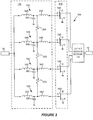
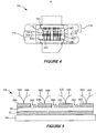
- FIG. 3 A schematic circuit diagram for a package 100 including an RF power transistor 115 and an input matching network 112 according to embodiments of the invention is illustrated in Figure 3 , and a physical layout of a package 100 according to embodiments of the invention is illustrated in Figure 4 .
- the RF power transistor 115 may comprise a single chip (die) or multiple chips (dice).
- a package 100 includes an RF transistor 115 including a plurality of parallel transistor cells 15A-D.
- Figure 3 illustrates an RF transistor 115 including four parallel cells 15A, 15B, 15C and 15D, it will be appreciated that the RF transistor 115 can have more than four, or less than four, parallel cells, according to embodiments of the invention.
- Each of the transistor cells 15A-D includes a control or input terminal and an output terminal.
- each of the transistor cells includes a gate G, a drain D and a source S.
- the gate G corresponds to the control or input terminal and the drain D corresponds to the output terminal, while the source S is grounded, as shown in Figure 3 .
- An input matching network 112 is connected between an RF signal input lead 14 and gates G of the transistor cells 15A-D.
- the input matching circuit 112 may include a plurality of inductive wire bond connections including bond wires extending between the RF signal input lead 14 and a capacitor block 136, and inductive wire bond connections including bond wires extending from the capacitor block 136 to the gates of the transistors 15A-D.
- the input matching network 112 includes a plurality of input matching circuits 12A to 12D, each of which is connected between the RF signal input lead 14 and a respective cell 15A-D of the RF transistor 115.
- Each of the input matching circuits 12A-D includes a first inductance 32A-D, a second inductance 34A-D and a capacitor 36A-D.
- the first inductance 32A-D can be provided by a wire bond connection between the RF input lead 14 and a terminal of a corresponding capacitor 36A-D.
- the second inductance 34A-D can be provided by a wire bond connection between the terminal of the corresponding capacitor 36A-D and an input terminal of a corresponding cell 15A-D of the RF transistor 115.
- a plurality of intra-capacitor resistors 35A to 35C are connected between input terminals of adjacent capacitors 36A-D of the input matching circuits 12A-D.
- the intra-capacitor resistors 35A to 35C may be provided, for example, as discrete surface mount resistors.
- the presence of the intra-capacitor resistors 35A to 35C may provide impedance matching with enhanced stability.
- Packaged transistors incorporating large periphery die typically need internal matching to improve usable bandwidth.
- adding an input capacitor as an internal input matching capacitor to the device can create a low frequency feedback path between adjacent cells of the large die, which can place a stability burden on the device.
- the internal matching circuitry of a large periphery power transistor may be carefully selected to avoid creating odd mode oscillations.
- selection of appropriate capacitor values and/or bond wire lengths (inductors) may place undesirable constraints on the matching network topology.
- the low frequency feedback path may be removed or attenuated while maintaining the impedance matching benefits of the input capacitor. Accordingly, design freedom of the capacitance and inductance values in the input matching circuits 12A to 12D may be increased.
- the capacitors 36A-D of the input matching network can be provided in a capacitor block 136 that can include discrete capacitor devices and/or can include a split capacitor, as illustrated in Figure 5 .
- the capacitor block 136 can include a split capacitor including a plurality of discrete input terminals 38A to 38D provided on a common dielectric 44 and a common ground terminal 42 on the base 140, as illustrated in Figures 4 and 5 .
- the wire bonds 32A-D connecting the RF input lead 14 to the input terminals 38A-D and the wire bonds 34A-D connecting the input terminals 38A-D to the input terminals of the respective transistor cells 15A-D are also partially illustrated in Figure 5 .
- a plurality of intra-capacitor resistors 35A to 35C are connected between input terminals 38A to 38D of adjacent capacitors 36A-D.
- the intra-capacitor resistors 35A to 35C may be provided, for example, as discrete surface mount resistors on the dielectric 44 between adjacent input terminals 38A to 38D.
- the output terminals of the transistor cells 15A to 15D are connected to the RF output lead 18 through an output matching network 116.
- the design of output matching networks is well known in the art, and need not be described in detail herein.
- the capacitor block 136 can be mounted on the base 140 of the package 100 adjacent to the transistor 15. It will be appreciated that the base of the package 100 can refer to any structural member on which the transistor 15 is mounted, and accordingly can correspond to a substrate, flange, die carrier, or the like.
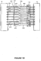
- FIG. 6 A schematic circuit diagram for a package 200 including an RF power transistor 115 and an input matching network 212 according to further embodiments of the invention is illustrated in Figure 6 , and a physical layout of a package 200 according to embodiments of the invention is illustrated in Figures 7A and 7B.
- Figure 7B is a magnified view illustrating some features of the package layout of Figure 7A in more detail.
- the input matching network 212 is connected between the RF signal input lead 14 and gates G of the transistor cells 15A-D of a power transistor 115, and includes a plurality of input matching circuits 40A to 40D, each of which is connected between the RF signal input lead 14 and a respective cell 15A-D of the RF transistor 115.
- a plurality of intra-capacitor resistors 45A-C are connected between input terminals of adjacent capacitors 46A-D of the input matching circuits 40A-D.
- the intra-capacitor resistors 45A-C may be provided on a separate resistor block 245 that may be provided on the base of the package 200 between the RF signal input lead 14 and a split capacitor block 236.
- the resistor block 245 may include a ceramic substrate 247, such as an alumina substrate, on which a plurality of series connected resistors 45A to 45C are mounted.
- the intra-capacitor resistors 45A to 45C may be provided, for example, as discrete surface mount resistors on the ceramic substrate 247.
- the resistor block 235 may include N number of nodes 47A to 47D, and N-1 number of resistors 45A to 45C may be coupled between respective pairs of the nodes 47A-D.
- the input matching circuit 212 may include a plurality of inductive wire bond connections including first bond wires 42A-D extending between the RF signal input lead 14 and respective resistors 45A-D in the resistor block 245, inductive wire bond connections including second bond wires 44A-D extending from respective resistors 45A-D in the resistor block 245 to respective capacitors 46A-D in the capacitor block 236, and inductive wire bond connections including third bond wires 48A-D extending from respective capacitors 46A-D in the capacitor block 236 to respective gates of the transistors 15A-D.
- each of the input matching circuits 40A-D includes a first inductance 42A-D, a second inductance 44A-D, a capacitor 46A-D and a third inductance 48A-D.
- the first inductance 42A-D can be provided by a wire bond connection between the RF input lead 14 and a respective node 47A-D of the resistor block 245.
- the second inductance 44A-D can be provided by a wirebond connection between a respective node 47A-D of the resistor block 245 and a terminal of a corresponding capacitor 46A-D.
- the third inductance 48A-D can be provided by a wire bond connection between the terminal of the corresponding capacitor 46A-D and an input terminal of a corresponding cell 15A-D of the RF transistor 115.
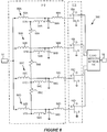
- FIG 8 A schematic circuit diagram for a package 300 including an RF power transistor 115 and an input matching network 312 according to further embodiments of the invention is illustrated in Figure 8 , and a physical layout of a package 300 according to embodiments of the invention is illustrated in Figures 9A and 9B.
- Figure 9B is a magnified view illustrating some features of the package layout of Figure 9A in more detail.
- the input matching network 312 is connected between the RF signal input lead 14 and gates G of the transistor cells 15A-D of a power transistor 115, and includes a plurality of input matching circuits 50A to 50D, each of which is connected between the RF signal input lead 14 and a respective cell 15A-D of the RF transistor 115.
- a plurality of intra-capacitor resistors 55A-C are connected between input terminals of adjacent capacitors 56A-D of the input matching circuits 50A-D.
- the intra-capacitor resistors 55A-C may be provided on a separate resistor block 345 that may be provided on the base of the package 300 between the RF signal input lead 14 and a split capacitor block 336.
- the resistor block 345 may include a ceramic substrate 347, such as an alumina substrate, on which a plurality of series connected resistors 55A to 55C are mounted.
- the intra-capacitor resistors 55A to 55C may be provided, for example, as discrete surface mount resistors on the ceramic substrate 347.
- the resistor block 335 may include N number of nodes 57A to 57D, and N-1 number of resistors 55A to 55C may be coupled between respective pairs of the nodes 57A-D.
- the input matching circuit 312 may include a plurality of inductive wire bond connections including first bond wires 52A-D extending between the RF signal input lead 14 and respective capacitors 56A-D in the capacitor block 336, inductive wire bond connections including second bond wires 54A-D extending from respective capacitors 56A-D in the capacitor block 336 to respective ones of the resistors 55A-D, and inductive wire bond connections including third bond wires 58A-D extending from respective capacitors 56A-D in the capacitor block 336 to respective gates of the transistors 15A-D.
- each of the input matching circuits 50A-D includes a first inductance 52A-D, a second inductance 54A-D, a capacitor 56A-D and a third inductance 58A-D.
- the first inductance 52A-D can be provided by a wire bond connection between the RF input lead 14 and a respective capacitor 56A-D of the capacitor block 3336.
- the second inductance 54A-D can be provided by a wirebond connection between a respective node 57A-D of the resistor block 345 and a terminal of a corresponding capacitor 56A-D.
- the third inductance 58A-D can be provided by a wire bond connection between the terminal of the corresponding capacitor 56A-D and a gate terminal of a corresponding cell 15A-D of the RF transistor 115.
- a capacitor block 136 including a split capacitor as shown in Figures 5 could be provided in the output matching circuit 116 according to some embodiments.
- an output terminal (e.g., the drain D) of each of the transistor cells 15A-D may be coupled to a corresponding input terminal 38A-D of a capacitor of the capacitor block 136, for example via an inductive bond wire.
- the input terminals 38A-D may likewise be coupled to the RF output lead 18, for example via an inductive bond wire.
- the lengths of the inductive bond wires and the capacitance of the capacitors in the capacitor block 136 may be chosen to provide a suitable impedance match at the output of the transistor die 115.
- a packaged RF power transistor according to embodiments of the invention may be useful in a wide range of applications in which stability is important.
- a packaged power transistor according to embodiments of the invention may have application in systems, such as WiMAX, WCDMA, CDMA, and/or other systems, including future (4th generation) systems.
- embodiments of the invention may be useful in any application in which stable operation is desired from a power transistor.
Landscapes
- Amplifiers (AREA)
Description
- This invention relates generally to RF transistors, and more particularly the invention relates to packaged RF transistors having input matching networks, and methods of forming packaged RF transistors having input matching networks.
- Packaged RF power devices typically include a transistor die mounted on a base and enclosed in a package. An RF input signal is supplied to the transistor through an RF input lead that extends from outside the package to the inside of the package, and an RF output signal is delivered from the device through an RF output lead that extends from inside the package to the outside. An input matching circuit can be included within the package, and can be connected between the RF input lead and an input terminal of the RF transistor. The input matching circuit provides an impedance match at the input of the transistor at the fundamental operating frequency of the transistor.
- The RF transistor can include a large periphery transistor die that includes a number of discrete transistor cells on a common substrate and connected in parallel. Input matching can be particularly beneficial for such devices, as it can increase the usable bandwidth of the devices. However, the input matching network typically includes a single capacitor, which can create a lower frequency feedback path between adjacent cells of the large periphery transistor die. This feedback path can reduce the stability of the overall device.
- Furthermore, the impedance values of elements of the input matching network must be carefully selected to avoid creating odd mode oscillations. Selection of the impedance values, including selection of appropriate inductances through bond wire lengths, can limit the topology of the matching network.
-
US 2008/315393 discloses a packaged RF transistor device that includes an RF transistor die including a plurality of RF transistor cells. The RF transistor device further includes an RF input lead, and an input matching network coupled between the RF input lead and the RF transistor die. -
US 6 137 367 discloses an amplifier for amplifying an input signal, and a high-voltage high-power embodiment of the amplifier. - In accordance with a first aspect there is provided a packaged RF transistor device, as described in claim 1. In accordance with a second aspect there is provided a method, as described in claim 8.
- In the following, only those embodiments unambiguously comprising all the features of one of claims 1 or 8 pertain to the invention, even if stated or suggested otherwise.
- A packaged RF transistor device according to some embodiments includes an RF transistor die including a plurality of RF transistor cells. Each of the plurality of RF transistor cells includes a control terminal and an output terminal. The RF transistor device further includes an RF input lead, and an input matching network coupled between the RF input lead and the RF transistor die. The input matching network includes a plurality of capacitors having respective input terminals. The input terminals of the capacitors are coupled to the control terminals of respective ones of the RF transistor cells. The input matching network further includes a plurality of resistors coupled respectively between adjacent input terminals of the capacitors.
- The input network may further include first wire bonds between the RF input lead and the input terminals of respective ones of the capacitors, and second wire bonds between the input terminals of respective ones of the capacitors and the control terminals of respective ones of the RF transistor cells.
- The input network may further include third wirebonds between the input terminals of the capacitors and respective terminals of the resistors.
- The plurality of resistors may be provided as a resistor block between the RF input lead and the RF transistor die, and the resistor block may include a plurality of nodes between respective ones of the resistors. The resistors may be connected in electrical series, and the third wirebonds may be coupled between respective ones of the nodes and the input terminals of the capacitors.
- In some embodiments, the input network may include first wire bonds between the RF input lead and terminals of the respective resistors, second wirebonds between the terminals of the resistors and the input terminals of respective ones of the capacitors, and third wire bonds between the input terminals of respective ones of the capacitors and the control terminals of respective ones of the RF transistor cells.
- The packaged RF transistor device may further include a base, and the RF transistor die may be mounted on the base between the RF input lead and the RF output lead. The plurality of resistors may be provided as a resistor block on the base between the RF input lead and the RF transistor die.
- The plurality of capacitors may be provided as a capacitor block on the base between the resistor block and the RF transistor die.
- The resistor block may include a plurality of nodes between respective ones of the resistors. The resistors may be connected in electrical series, and the second wirebonds may be coupled between respective ones of the nodes and the input terminals of the capacitors.
- The packaged RF transistor device may further include an RF output lead coupled to the output terminals of respective ones of the RF transistor cells, and a base. The RF transistor die may be mounted on the base between the RF input lead and the RF output lead. The plurality of capacitors may be provided as a capacitor block on the base between the RF input lead and the RF transistor die, and the plurality of resistors may be provided as a resistor block on the base between the RF input lead and the capacitor block. The device may further include a package that houses the RF transistor die and the input matching network, with the RF signal input lead and the RF signal output lead extending from the package.
- The capacitor block may include a common ground terminal and a plurality of discrete input terminals, and may further include a common dielectric. In some embodiments, the plurality of capacitors include a plurality of discrete devices.
- A packaged RF transistor device according to further embodiments includes an RF transistor die including a plurality of RF transistor cells. Each of the plurality of RF transistor cells includes a control terminal and an output terminal. The packaged RF transistor device further includes an RF input lead and an input matching network coupled between the RF input lead and the RF transistor die. The input matching network includes a split capacitor having a plurality of input terminals. The input terminals of the split capacitor are coupled to the control terminals of respective ones of the RF transistor cells. The input matching network further includes a plurality of resistors coupled respectively between adjacent input terminals of the split capacitor.
- The input network may further include first wire bonds between the RF input lead and respective input terminals of the split capacitor, and second wire bonds between the respective input terminals of the split capacitor and the control terminals of respective ones of the RF transistor cells.
- The packaged RF transistor device may further include an RF output lead coupled to the output terminals of respective ones of the RF transistor cells, and a package that houses the RF transistor die and the input matching network, with the RF signal input lead and the RF signal output lead extending from the package.
- The packaged RF transistor device may further include a base, and the RF transistor die may be mounted on the base between the RF input lead and the RF output lead. The split capacitor may be on the base between the RF input lead and the RF transistor die. The split capacitor may include a common ground terminal and/or a common dielectric.
- Some embodiments of the invention provide methods of forming a packaged RF transistor device. The methods include mounting a transistor including a plurality of RF transistor cells on a base. Each of the plurality of RF transistor cells includes a control terminal and an output terminal. The methods further include mounting a plurality of capacitors having respective input terminals on the base, coupling the input terminals of the capacitors to the control terminals of respective ones of the RF transistor cells, coupling a plurality of resistors respectively between adjacent input terminals of the capacitors, and coupling an RF input lead to the input terminals of the capacitors.
- The methods may further include forming a package housing on the base, the housing enclosing the transistor and the plurality of capacitors, with the RF input lead extending from the package. Coupling the RF input lead to the input terminals of the capacitors may include forming first wire bonds between the RF input lead and the input terminals of respective ones of the capacitors, and coupling the input terminals of the capacitors to the control terminals of respective ones of the RF transistor cells may include forming second wire bonds between the input terminals of respective ones of the capacitors and the control terminals of respective ones of the RF transistor cells.
- The methods may further include coupling an RF output lead to the output terminals of respective ones of the RF transistor cells, and forming a package housing that houses the RF transistor die and the plurality of capacitors, with the RF signal input lead and the RF signal output lead extending from the package.
- The methods may further include mounting the RF transistor die on the base between the RF input lead and the RF output lead, and mounting the plurality of capacitors may include mounting a capacitor block on the base between the RF input lead and the RF transistor die. The capacitor block may include a common ground terminal and a plurality of discrete input terminals. The capacitor block may further include a common dielectric. In some embodiments, the plurality of capacitors may include a plurality of discrete devices.
- The methods may further include forming third wirebonds between the input terminals of the capacitors and respective terminals of the resistors.
- The plurality of resistors may be provided as a resistor block between the RF input lead and the RF transistor die, and the resistor block may include a plurality of nodes between respective ones of the resistors. The resistors may be connected in electrical series, and the third wirebonds may be coupled between respective ones of the nodes and the input terminals of the capacitors.
- The input network may further include first wire bonds between the RF input lead and terminals of the respective resistors, second wirebonds between the terminals of the resistors and the input terminals of respective ones of the capacitors, and third wire bonds between the input terminals of respective ones of the capacitors and the control terminals of respective ones of the RF transistor cells.
- The methods may further include providing a base, and the RF transistor die may be mounted on the base between the RF input lead and the RF output lead, and the plurality of resistors may be provided as a resistor block on the base between the RF input lead and the RF transistor die.
- The plurality of capacitors may be provided as a capacitor block on the base between the resistor block and the RF transistor die.
- According to further embodiments of the invention, a packaged RF transistor device includes an RF transistor die including a plurality of RF transistor cells, each of the plurality of RF transistor cells including a control terminal and an output terminal, an RF input lead and an RF output lead, and a matching network coupled between the RF input lead or the RF output lead and the RF transistor die. The matching network includes a plurality of capacitors having respective input terminals. The input terminals of the capacitors are coupled to corresponding control terminals or output terminals of respective ones of the RF transistor cells. The input matching network further includes a plurality of resistors coupled respectively between adjacent input terminals of the capacitors.
- In some embodiments, the matching network includes an output matching network coupled between the RF output lead and the RF transistor die, and the input terminals of the capacitors are coupled to corresponding output terminals of respective ones of the RF transistor cells.
- The accompanying drawings, which are included to provide a further understanding of the invention and are incorporated in and constitute a part of this application, illustrate certain embodiment(s) of the invention. In the drawings:
-
Figure 1 is a functional block diagram of a conventional RF power transistor. -
Figure 2A is a perspective view of a packaged RF power transistor according to some embodiments of the invention. -
Figure 2B is a functional block diagram of a packaged RF power transistor according to some embodiments of the invention. -
Figure 3 is a schematic circuit diagram of a packaged RF power transistor according to some embodiments of the invention. -
Figure 4 is a plan view of a layout of a packaged RF power transistor according to some embodiments of the invention. -
Figure 5 is a cross sectional view of a split capacitor in accordance with some embodiments of the invention. -
Figure 6 is a schematic circuit diagram of a packaged RF power transistor according to further embodiments of the invention. -
Figures 7A and7B are a plan views of a layout of a packaged RF power transistor according to further embodiments of the invention. -
Figure 8 is a schematic circuit diagram of a packaged RF power transistor according to further embodiments of the invention. -
Figures 9A and9B are a plan views of a layout of a packaged RF power transistor according to further embodiments of the invention. - Embodiments of the present invention now will be described more fully hereinafter with reference to the accompanying drawings, in which embodiments of the invention are shown. This invention may, however, be embodied in many different forms and should not be construed as limited to the embodiments set forth herein. Rather, these embodiments are provided so that this disclosure will be thorough and complete, and will fully convey the scope of the invention to those skilled in the art. Like numbers refer to like elements throughout.
- It will be understood that, although the terms first, second, etc. may be used herein to describe various elements, these elements should not be limited by these terms. These terms are only used to distinguish one element from another. For example, a first element could be termed a second element, and, similarly, a second element could be termed a first element, without departing from the scope of the present invention. As used herein, the term "and/or" includes any and all combinations of one or more of the associated listed items.
- The terminology used herein is for the purpose of describing particular embodiments only and is not intended to be limiting of the invention. As used herein, the singular forms "a", "an" and "the" are intended to include the plural forms as well, unless the context clearly indicates otherwise. It will be further understood that the terms "comprises," "comprising," "includes" and/or "including" when used herein, specify the presence of stated features, integers, steps, operations, elements, and/or components, but do not preclude the presence or addition of one or more other features, integers, steps, operations, elements, components, and/or groups thereof.
- Unless otherwise defined, all terms (including technical and scientific terms) used herein have the same meaning as commonly understood by one of ordinary skill in the art to which this invention belongs. It will be further understood that terms used herein should be interpreted as having a meaning that is consistent with their meaning in the context of this specification and the relevant art and will not be interpreted in an idealized or overly formal sense unless expressly so defined herein.
- It will be understood that when an element is referred to as being "on" or extending "onto" another element, it can be directly on or extend directly onto the other element or intervening elements may also be present. In contrast, when an element is referred to as being "directly on" or extending "directly onto" another element, there are no intervening elements present. It will also be understood that when an element is referred to as being "connected" or "coupled" to another element, it can be directly connected or coupled to the other element or intervening elements may be present. In contrast, when an element is referred to as being "directly connected" or "directly coupled" to another element, there are no intervening elements present.
- Relative terms such as "below" or "above" or "upper" or "lower" or "horizontal" or "lateral" or "vertical" may be used herein to describe a relationship of one element, layer or region to another element, layer or region as illustrated in the figures. It will be understood that these terms are intended to encompass different orientations of the device in addition to the orientation depicted in the figures.
- Some embodiments of the invention provide packaged RF power transistors. RF power transistors typically include a plurality of transistor cells operating in parallel. Transistors that can be included in packages according to embodiments of the invention can include laterally diffused MOSFETS (LDMOSFET) or other semiconductor devices, such as bipolar devices, MESFET devices, HBTs and HEMT devices. The transistors can be made using narrow or wide bandgap semiconductors. For example, the transistors can include silicon LDMOS and/or bipolar transistors, and/or III-V devices such as GaAs MESFETs, InGaP HBTs, GaN HEMT devices, GaN bipolar transistors, etc.
- RF power transistors providing 10 watts or more of power can be packaged as discrete devices, as shown schematically at 10 in
Figure 1 . The packaged transistor 15 (which may include a FET or bipolar device, for example) normally includes aninput matching circuit 12 connecting anRF input lead 14 to a control electrode of the transistor 15 (e.g., a gate G of a FET or a base of a bipolar transistor). Thetransistor 15 may be a large periphery RF transistor including a plurality of transistor cells connected in parallel. AnRF output lead 18 is connected to an output electrode of the transistor 15 (e.g., the drain D of a FET or the collector or emitter of a bipolar transistor). TheRF input lead 14 and theRF output lead 18 extend outside thepackage 10, as shown inFigure 1 . The source S of theFET 15 may be grounded. - A packaged
transistor 10 may be mounted on a printed circuit board (not shown). An external output matching circuit (not shown) may also be mounted on the printed circuit board. A bias/RF diplexer (not shown) may be connected to the external output matching circuit to connect the transistor output to an RF output. Furthermore, a DC power supply (not shown) may be connected to the transistor'sRF output lead 18. - Internal matching networks have been provided within RF power transistor packages, as illustrated in
Figure 1 . However, such internal matching networks typically include a single capacitor. As explained above, including the capacitor within the device package can create a lower frequency feedback path between adjacent cells of a large periphery transistor die, which can reduce the stability of the overall device. - According to some embodiments of the invention, an internal matching network of a packaged RF transistor includes a plurality of parallel capacitors. Wirebond connections are provided from the plurality of the capacitors to respective cells of a multi-cell RF transistor die.
- For example, an internal matching network can include a split capacitor and/or multiple capacitors on the base of the package adjacent the multi-cell RF transistor die. Providing an input matching network including a plurality of parallel capacitors can reduce and/or remove the low frequency feedback path(s), which can improve the stability of the packaged device.
- A packaged
RF transistor 100 according to some embodiments of the invention is shown generally inFigure 2A and schematically inFigure 2B . As shown therein, the packagedtransistor 100 includes anRF input lead 14 and anRF output lead 18 that extend outside the package. TheRF input lead 14 is connected through aninput matching circuit 112 to a control terminal (such as the gate G) of atransistor 115, which can include a plurality of transistor cells connected in parallel. An output terminal (such as the drain D) of thetransistor 115 is connected to theRF output lead 18. According to some embodiments, the input matching circuit includes multiple capacitors. Respective ones of the capacitors in the input matching circuit may be coupled to a respective transistor cell of theRF transistor 115. - A schematic circuit diagram for a
package 100 including anRF power transistor 115 and aninput matching network 112 according to embodiments of the invention is illustrated inFigure 3 , and a physical layout of apackage 100 according to embodiments of the invention is illustrated inFigure 4 . TheRF power transistor 115 may comprise a single chip (die) or multiple chips (dice). Referring toFigures 3 and4 , apackage 100 includes anRF transistor 115 including a plurality ofparallel transistor cells 15A-D. AlthoughFigure 3 illustrates anRF transistor 115 including fourparallel cells RF transistor 115 can have more than four, or less than four, parallel cells, according to embodiments of the invention. Each of thetransistor cells 15A-D includes a control or input terminal and an output terminal. For example, in embodiments including a FET device, each of the transistor cells includes a gate G, a drain D and a source S. In some embodiments, the gate G corresponds to the control or input terminal and the drain D corresponds to the output terminal, while the source S is grounded, as shown inFigure 3 . - An
input matching network 112 is connected between an RFsignal input lead 14 and gates G of thetransistor cells 15A-D. Theinput matching circuit 112 may include a plurality of inductive wire bond connections including bond wires extending between the RFsignal input lead 14 and acapacitor block 136, and inductive wire bond connections including bond wires extending from thecapacitor block 136 to the gates of thetransistors 15A-D. - The
input matching network 112 includes a plurality ofinput matching circuits 12A to 12D, each of which is connected between the RFsignal input lead 14 and arespective cell 15A-D of theRF transistor 115. Each of theinput matching circuits 12A-D includes afirst inductance 32A-D, asecond inductance 34A-D and acapacitor 36A-D. As illustrated inFigure 4 , thefirst inductance 32A-D can be provided by a wire bond connection between theRF input lead 14 and a terminal of acorresponding capacitor 36A-D. Thesecond inductance 34A-D can be provided by a wire bond connection between the terminal of thecorresponding capacitor 36A-D and an input terminal of acorresponding cell 15A-D of theRF transistor 115. - A plurality of
intra-capacitor resistors 35A to 35C are connected between input terminals ofadjacent capacitors 36A-D of theinput matching circuits 12A-D. Theintra-capacitor resistors 35A to 35C may be provided, for example, as discrete surface mount resistors. - The presence of the
intra-capacitor resistors 35A to 35C may provide impedance matching with enhanced stability. Packaged transistors incorporating large periphery die typically need internal matching to improve usable bandwidth. However, adding an input capacitor as an internal input matching capacitor to the device can create a low frequency feedback path between adjacent cells of the large die, which can place a stability burden on the device. The internal matching circuitry of a large periphery power transistor may be carefully selected to avoid creating odd mode oscillations. However, selection of appropriate capacitor values and/or bond wire lengths (inductors) may place undesirable constraints on the matching network topology. - By providing the input capacitor input as a plurality of individual capacitors with intra-capacitor resistors coupled between the individual capacitors, the low frequency feedback path may be removed or attenuated while maintaining the impedance matching benefits of the input capacitor. Accordingly, design freedom of the capacitance and inductance values in the
input matching circuits 12A to 12D may be increased. - The
capacitors 36A-D of the input matching network can be provided in acapacitor block 136 that can include discrete capacitor devices and/or can include a split capacitor, as illustrated inFigure 5 . Referring toFigure 5 , thecapacitor block 136 can include a split capacitor including a plurality ofdiscrete input terminals 38A to 38D provided on acommon dielectric 44 and acommon ground terminal 42 on thebase 140, as illustrated inFigures 4 and 5 . The wire bonds 32A-D connecting theRF input lead 14 to theinput terminals 38A-D and thewire bonds 34A-D connecting theinput terminals 38A-D to the input terminals of therespective transistor cells 15A-D are also partially illustrated inFigure 5 . A plurality ofintra-capacitor resistors 35A to 35C are connected betweeninput terminals 38A to 38D ofadjacent capacitors 36A-D. Theintra-capacitor resistors 35A to 35C may be provided, for example, as discrete surface mount resistors on the dielectric 44 betweenadjacent input terminals 38A to 38D. - In the embodiments illustrated in
Figures 3 and4 , the output terminals of thetransistor cells 15A to 15D are connected to theRF output lead 18 through anoutput matching network 116. The design of output matching networks is well known in the art, and need not be described in detail herein. - As shown in
Figure 4 , thecapacitor block 136 can be mounted on thebase 140 of thepackage 100 adjacent to thetransistor 15. It will be appreciated that the base of thepackage 100 can refer to any structural member on which thetransistor 15 is mounted, and accordingly can correspond to a substrate, flange, die carrier, or the like. - A schematic circuit diagram for a
package 200 including anRF power transistor 115 and aninput matching network 212 according to further embodiments of the invention is illustrated inFigure 6 , and a physical layout of apackage 200 according to embodiments of the invention is illustrated inFigures 7A and7B. Figure 7B is a magnified view illustrating some features of the package layout ofFigure 7A in more detail. - Referring to
Figures 6 ,7A and7B , theinput matching network 212 is connected between the RFsignal input lead 14 and gates G of thetransistor cells 15A-D of apower transistor 115, and includes a plurality of input matching circuits 40A to 40D, each of which is connected between the RFsignal input lead 14 and arespective cell 15A-D of theRF transistor 115. In the embodiments illustrated inFigures 6 ,7A and7B , a plurality ofintra-capacitor resistors 45A-C are connected between input terminals ofadjacent capacitors 46A-D of the input matching circuits 40A-D. - The
intra-capacitor resistors 45A-C may be provided on aseparate resistor block 245 that may be provided on the base of thepackage 200 between the RFsignal input lead 14 and asplit capacitor block 236. Theresistor block 245 may include aceramic substrate 247, such as an alumina substrate, on which a plurality of series connectedresistors 45A to 45C are mounted. Theintra-capacitor resistors 45A to 45C may be provided, for example, as discrete surface mount resistors on theceramic substrate 247. - The resistor block 235 may include N number of
nodes 47A to 47D, and N-1 number ofresistors 45A to 45C may be coupled between respective pairs of thenodes 47A-D. - The
input matching circuit 212 may include a plurality of inductive wire bond connections includingfirst bond wires 42A-D extending between the RFsignal input lead 14 andrespective resistors 45A-D in theresistor block 245, inductive wire bond connections includingsecond bond wires 44A-D extending fromrespective resistors 45A-D in theresistor block 245 torespective capacitors 46A-D in thecapacitor block 236, and inductive wire bond connections includingthird bond wires 48A-D extending fromrespective capacitors 46A-D in thecapacitor block 236 to respective gates of thetransistors 15A-D. - Stated differently, each of the input matching circuits 40A-D includes a
first inductance 42A-D, asecond inductance 44A-D, acapacitor 46A-D and athird inductance 48A-D. As illustrated inFigure 6 , thefirst inductance 42A-D can be provided by a wire bond connection between theRF input lead 14 and arespective node 47A-D of theresistor block 245. Thesecond inductance 44A-D can be provided by a wirebond connection between arespective node 47A-D of theresistor block 245 and a terminal of acorresponding capacitor 46A-D. Thethird inductance 48A-D can be provided by a wire bond connection between the terminal of thecorresponding capacitor 46A-D and an input terminal of acorresponding cell 15A-D of theRF transistor 115. - A schematic circuit diagram for a
package 300 including anRF power transistor 115 and aninput matching network 312 according to further embodiments of the invention is illustrated inFigure 8 , and a physical layout of apackage 300 according to embodiments of the invention is illustrated inFigures 9A and9B. Figure 9B is a magnified view illustrating some features of the package layout ofFigure 9A in more detail. - Referring to
Figures 8 ,9A and9B , theinput matching network 312 is connected between the RFsignal input lead 14 and gates G of thetransistor cells 15A-D of apower transistor 115, and includes a plurality ofinput matching circuits 50A to 50D, each of which is connected between the RFsignal input lead 14 and arespective cell 15A-D of theRF transistor 115. In the embodiments illustrated inFigures 8 ,9A and9B , a plurality ofintra-capacitor resistors 55A-C are connected between input terminals ofadjacent capacitors 56A-D of theinput matching circuits 50A-D. - The
intra-capacitor resistors 55A-C may be provided on aseparate resistor block 345 that may be provided on the base of thepackage 300 between the RFsignal input lead 14 and asplit capacitor block 336. Theresistor block 345 may include aceramic substrate 347, such as an alumina substrate, on which a plurality of series connectedresistors 55A to 55C are mounted. Theintra-capacitor resistors 55A to 55C may be provided, for example, as discrete surface mount resistors on theceramic substrate 347. - The resistor block 335 may include N number of
nodes 57A to 57D, and N-1 number ofresistors 55A to 55C may be coupled between respective pairs of thenodes 57A-D. - The
input matching circuit 312 may include a plurality of inductive wire bond connections includingfirst bond wires 52A-D extending between the RFsignal input lead 14 andrespective capacitors 56A-D in thecapacitor block 336, inductive wire bond connections includingsecond bond wires 54A-D extending fromrespective capacitors 56A-D in thecapacitor block 336 to respective ones of theresistors 55A-D, and inductive wire bond connections includingthird bond wires 58A-D extending fromrespective capacitors 56A-D in thecapacitor block 336 to respective gates of thetransistors 15A-D. - Stated differently, each of the
input matching circuits 50A-D includes afirst inductance 52A-D, asecond inductance 54A-D, acapacitor 56A-D and athird inductance 58A-D. As illustrated inFigure 8 , thefirst inductance 52A-D can be provided by a wire bond connection between theRF input lead 14 and arespective capacitor 56A-D of the capacitor block 3336. Thesecond inductance 54A-D can be provided by a wirebond connection between arespective node 57A-D of theresistor block 345 and a terminal of acorresponding capacitor 56A-D. Thethird inductance 58A-D can be provided by a wire bond connection between the terminal of thecorresponding capacitor 56A-D and a gate terminal of acorresponding cell 15A-D of theRF transistor 115. - While configurations have been described primarily in connection with an input matching circuit, other configurations may be used in an output matching circuit, such as the
output matching circuit 116 illustrated inFigures 3 ,4 ,6 and8 . For example, acapacitor block 136 including a split capacitor as shown inFigures 5 could be provided in theoutput matching circuit 116 according to some embodiments. In such embodiments, an output terminal (e.g., the drain D) of each of thetransistor cells 15A-D may be coupled to acorresponding input terminal 38A-D of a capacitor of thecapacitor block 136, for example via an inductive bond wire. Theinput terminals 38A-D may likewise be coupled to theRF output lead 18, for example via an inductive bond wire. The lengths of the inductive bond wires and the capacitance of the capacitors in thecapacitor block 136 may be chosen to provide a suitable impedance match at the output of the transistor die 115. - Furthermore, while embodiments of the present application have been described primarily in connection with packaged RF transistors including a single transistor die,
multiple transistor dice 115 could be included in asingle package 100, with a capacitor block including multiple capacitors provided for one or more of the transistor. - A packaged RF power transistor according to embodiments of the invention may be useful in a wide range of applications in which stability is important. For example, a packaged power transistor according to embodiments of the invention may have application in systems, such as WiMAX, WCDMA, CDMA, and/or other systems, including future (4th generation) systems. In general, embodiments of the invention may be useful in any application in which stable operation is desired from a power transistor.
Claims (22)
- A packaged RF transistor device (100), comprising:an RF transistor die including a plurality of RF transistor cells (15A-D), each of the plurality of RF transistor cells (15A-D) including a control terminal and an output terminal;an RF input lead (14); andan input matching network (112) coupled between the RF input lead (14) and the RF transistor die, the input matching network (112) comprises at least one of: (a) a plurality of capacitors (36A-D) having respective input terminals, wherein the input terminals of the capacitors (36A-D) are coupled to the control terminals of respective ones of the RF transistor cells (15A-D), and wherein the input matching network (112) further comprises a plurality of resistors (35A-C) coupled respectively between adjacent input terminals of the capacitors (36A-D); and (b) a split capacitor comprising a plurality of input terminals, wherein the input terminals of the split capacitor are coupled to the control terminals of respective ones of the RF transistor cells (15A-D), and wherein the input matching network (112) further comprises a plurality of resistors (35A-C) coupled respectively between adjacent input terminals of the split capacitor.
- The packaged RF transistor device of Claim 1, wherein the input matching network (112) comprises a plurality of capacitors (36A-D) having respective input terminals, wherein the input terminals of the capacitors (36A-D) are coupled to the control terminals of respective ones of the RF transistor cells (15A-D), and wherein the input matching network (112) further comprises a plurality of resistors (35A-C) coupled respectively between adjacent input terminals of the capacitors (36A-D), and further comprises first wire bonds (32A-D) between the RF input lead (14) and the input terminals of respective ones of the capacitors (36A-D) and second wire bonds (34A-D) between the input terminals of respective ones of the capacitors (36A-D) and the control terminals of respective ones of the RF transistor cells (15A-D).
- The packaged RF transistor device of Claim 1, further comprising a base, wherein the RF transistor die is mounted on the base between the RF input lead (14) and an RF output lead (18), and wherein the plurality of resistors (35A-C) is provided as a resistor block (245) on the base between the RF input lead (14) and the RF transistor die.
- The packaged RF transistor device of Claim 3, wherein the plurality of capacitors (36A-D) is provided as a capacitor block (136) on the base between the resistor block (245) and the RF transistor die.
- The packaged RF transistor device of Claim 3, wherein the resistor block (245) comprises a plurality of nodes (47A-D) between respective ones of the resistors (45A-C), the resistors (45A-C) are connected in electrical series, and the second wirebonds (44A-D) are coupled between respective ones of the nodes (47A-D) and the input terminals of the capacitors (46A-D).
- The packaged RF transistor device of Claim 1, wherein the input matching network (112) comprises a plurality of capacitors (36A-D) having respective input terminals, wherein the input terminals of the capacitors (36A-D) are coupled to the control terminals of respective ones of the RF transistor cells (15A-D), and wherein the input matching network (112) further comprises a plurality of resistors (35A-D) coupled respectively between adjacent input terminals of the capacitors (36A-D), and wherein the RF transistor device (100) further comprises:an RF output lead (18) coupled to the output terminals of respective ones of the RF transistor cells (15A-D);a base, wherein the RF transistor die is mounted on the base between the RF input lead (14) and the RF output lead (18), wherein the plurality of capacitors (36A-D) is provided as a capacitor block (136) on the base (140) between the RF input lead (14) and the RF transistor die and wherein the plurality of resistors (35A-C) is provided as a resistor block (245) on the base between the RF input lead (14) and the capacitor block (136); anda package that houses the RF transistor die and the input matching network (112), with the RF signal input lead (14) and the RF signal output lead (18) extending from the package.
- The packaged RF transistor device (100) of Claim 1, wherein the plurality of resistors (35A-C) comprises a plurality of discrete devices.
- A method configured for forming the packaged RF transistor device (100) of Claim 1, comprising:mounting a transistor on a base (140), the transistor (115) including a plurality of RF transistor cells (15A-D), each of the plurality of RF transistor cells (15A-D) including a control terminal and an output terminal;mounting a plurality of capacitors (36A-D) having respective input terminals on the base (140);coupling the input terminals of the capacitors (36A-D) to the control terminals of respective ones of the RF transistor cells (15A-D);coupling a plurality of resistors (35A-C) between adjacent input terminals of the capacitors (36A-D); andcoupling an RF input lead (14) to the input terminals of the capacitors (36A-D).
- The method of Claim 8, further comprising:
forming a package housing on the base (140), the housing enclosing the transistor (115) and the plurality of capacitors (36A-D), with the RF input lead (14) extending from the package. - The method of Claim 8, wherein coupling the RF input lead (14) to the input terminals of the capacitors (36A-D) comprises forming first wire bonds (32A-D) between the RF input lead (14) and the input terminals of respective ones of the capacitors (36A-D), and coupling the input terminals of the capacitors (36A-D) to the control terminals of respective ones of the RF transistor cells comprises forming second wire bonds (34A-D) between the input terminals of respective ones of the capacitors (36A-D) and the control terminals of respective ones of the RF transistor cells (15A-D).
- The method of Claim 8, further comprising:coupling an RF output lead (18) to the output terminals of respective ones of the RF transistor cells (15A-D); andforming a package housing that houses the RF transistor die and the plurality of capacitors (36A-D), with the RF input lead (14) and the RF output lead (18) extending from the package.
- The method of Claim 11, further comprising mounting the RF transistor die on the base between the RF input lead (14) and the RF output lead (18), and wherein mounting the plurality of capacitors (36A-D) comprises mounting a capacitor block (136) on the base between the RF input lead (14) and the RF transistor die.
- The method of Claim 12, wherein the plurality of resistors (45A-C) is provided as a resistor block (245) between the RF input lead (14) and the RF transistor die, and wherein the resistor block (245) comprises a plurality of nodes (47A-D) between respective ones of the resistors (45A-C), the resistors (45A-C) are connected in electrical series, and wirebonds are coupled between respective ones of the nodes (47A-D) and the input terminals of the capacitors (46A-D).
- The method of Claim 8, further comprising providing a base and mounting the RF transistor die on the base between the RF input lead (14) and an RF output lead (18), and wherein the plurality of resistors (35A-C) is provided as a resistor block (245) on the base between the RF input lead (14) and the RF transistor die.
- The method of Claim 14, wherein the plurality of capacitors (36A-D) is provided as a capacitor block (136) on the base between the resistor block (245) and the RF transistor die.
- The packaged RF transistor device of Claim 2, wherein the input matching network (212) further comprises third wirebonds (48A-D) between the input terminals of the capacitors (46A-D) and respective terminals of the resistors (45A-C).
- The packaged RF transistor device of Claim 16, wherein the plurality of resistors (45A-C) is provided as a resistor block (245) between the RF input lead (14) and the RF transistor die, and wherein the resistor block (245) comprises a plurality of nodes (47A-D) between respective ones of the resistors (45A-C), the resistors (45A-C) are connected in electrical series, and the third wirebonds (48A-C) are coupled between respective ones of the nodes (47A-D) and the input terminals of the capacitors (46A-D).
- The packaged RF transistor device of Claim 1, wherein the input matching network (212) comprises a plurality of capacitors (46A-D) having respective input terminals, wherein the input terminals of the capacitors (46A-D) are coupled to the control terminals of respective ones of the RF transistor cells (15A-D), and wherein the input matching network (212) further comprises a plurality of resistors (45A-C) coupled respectively between adjacent input terminals of the capacitors (46A-D), and further comprises first wire bonds (42A-D) between the RF input lead (14) and terminals of respective ones of the resistors (45A-C), second wire bonds (44A-D) between the terminals of respective ones of the resistors (45A-C) and the input terminals of respective ones of the capacitors (46A-D), and third wirebonds (48A-D) between the input terminals of respective ones of the capacitors (46A-D) and the control terminals of respective ones of the RF transistor cells (15A-D).
- The packaged RF transistor device of Claim 1, wherein the input matching network (112) comprises a split capacitor including a plurality of input terminals, wherein the input terminals of the split capacitor are coupled to the control terminals of respective ones of the RF transistor cells (15A-D), and wherein the input matching network (112) further comprises a plurality of resistors (35A-C) coupled respectively between adjacent input terminals of the split capacitor, and further comprises first wire bonds (32A-D) between the RF input lead (14) and the respective input terminals of the split capacitor, second wire bonds (34A-D) between the respective input terminals of the split capacitor and the control terminals of respective ones of the RF transistor cells (15A-D).
- The method of claim 10, further comprising forming third wirebonds (48A-D) between the input terminals of the capacitors (46A-D) and respective terminals of the resistors (45A-C).
- The method of claim 8, wherein coupling the RF input lead (14) to the input terminals of the capacitors (46A-D) comprises forming first wire bonds (42A-D) between the RF input lead (14) and terminals of respective ones of the resistors (45A-C) and forming second wire bonds (44A-D) between the terminals of respective ones of the resistors (45A-C) and the input terminals of respective ones of the capacitors (46A-D), and
wherein coupling the input terminals of the capacitors (46A-D) to the control terminals of respective ones of the RF transistor cells (15A-D) comprises forming third wire bonds (48A-D) between the input terminals of respective ones of the capacitors (46A-D) and the control terminals of respective ones of the RF transistor cells (15A-D). - The packaged RF transistor device of Claim 1, wherein the input matching network (112) comprises a plurality of capacitors (36A-D) having respective input terminals, wherein the input terminals of the capacitors (36A-D) are coupled to the control terminals of respective ones of the RF transistor cells (15A-D), and wherein the input matching network (112) further comprises a plurality of resistors (35A-C) coupled respectively between adjacent input terminals of the capacitors (36A-D), and wherein each RF transistor cell (15A-D) is connected to a different one of the plurality of discrete capacitors.
Applications Claiming Priority (2)
| Application Number | Priority Date | Filing Date | Title |
|---|---|---|---|
| US12/962,923 US8592966B2 (en) | 2007-06-22 | 2010-12-08 | RF transistor packages with internal stability network including intra-capacitor resistors and methods of forming RF transistor packages with internal stability networks including intra-capacitor resistors |
| PCT/US2011/061638 WO2012078346A1 (en) | 2010-12-08 | 2011-11-21 | Rf transistor packages with internal stability network including intra-capacitor resistors and methods of forming rf transistor packages with internal stability networks including intra-capacitor resistors |
Publications (3)
| Publication Number | Publication Date |
|---|---|
| EP2649549A1 EP2649549A1 (en) | 2013-10-16 |
| EP2649549A4 EP2649549A4 (en) | 2017-01-11 |
| EP2649549B1 true EP2649549B1 (en) | 2020-07-01 |
Family
ID=46207457
Family Applications (1)
| Application Number | Title | Priority Date | Filing Date |
|---|---|---|---|
| EP11847818.9A Active EP2649549B1 (en) | 2010-12-08 | 2011-11-21 | Rf transistor packages with internal stability network including intra-capacitor resistors and methods of forming rf transistor packages with internal stability networks including intra-capacitor resistors |
Country Status (5)
| Country | Link |
|---|---|
| US (1) | US8592966B2 (en) |
| EP (1) | EP2649549B1 (en) |
| JP (1) | JP5848360B2 (en) |
| CN (1) | CN103339637B (en) |
| WO (1) | WO2012078346A1 (en) |
Families Citing this family (21)
| Publication number | Priority date | Publication date | Assignee | Title |
|---|---|---|---|---|
| US9741673B2 (en) * | 2007-06-22 | 2017-08-22 | Cree, Inc. | RF transistor packages with high frequency stabilization features and methods of forming RF transistor packages with high frequency stabilization features |
| US9281748B2 (en) | 2012-03-02 | 2016-03-08 | Lenovo Enterprise Solutions (Singapore) Pte. Ltd. | Operating a DC-DC converter |
| CN104396141B (en) * | 2012-06-29 | 2018-04-10 | 克里公司 | The radio frequency crystals tube device of encapsulation |
| US9236347B2 (en) | 2013-10-09 | 2016-01-12 | Lenovo Enterprise Solutions (Singapore) Pte. Ltd. | Operating and manufacturing a DC-DC converter |
| KR101695320B1 (en) | 2014-03-18 | 2017-01-13 | 한국전자통신연구원 | Component package including matching circuit and matching method thereof |
| US9641163B2 (en) | 2014-05-28 | 2017-05-02 | Cree, Inc. | Bandwidth limiting methods for GaN power transistors |
| US9472480B2 (en) | 2014-05-28 | 2016-10-18 | Cree, Inc. | Over-mold packaging for wide band-gap semiconductor devices |
| US9515011B2 (en) | 2014-05-28 | 2016-12-06 | Cree, Inc. | Over-mold plastic packaged wide band-gap power transistors and MMICS |
| US9245837B1 (en) * | 2014-07-07 | 2016-01-26 | Infineon Technologies Ag | Radio frequency power device |
| US9219422B1 (en) | 2014-08-21 | 2015-12-22 | Lenovo Enterprise Solutions (Singapore) Pte. Ltd. | Operating a DC-DC converter including a coupled inductor formed of a magnetic core and a conductive sheet |
| US9589927B2 (en) * | 2014-09-19 | 2017-03-07 | Nxp Usa, Inc. | Packaged RF amplifier devices with grounded isolation structures and methods of manufacture thereof |
| US9379619B2 (en) | 2014-10-21 | 2016-06-28 | Lenovo Enterprise Solutions (Singapore) Pte. Ltd. | Dividing a single phase pulse-width modulation signal into a plurality of phases |
| US9618539B2 (en) | 2015-05-28 | 2017-04-11 | Lenovo Enterprise Solutions (Singapore) Pte. Ltd. | Sensing current of a DC-DC converter |
| CN105810647B (en) * | 2016-04-22 | 2018-11-06 | 宜确半导体(苏州)有限公司 | RF switch integration module and its integrated approach, radio-frequency front-end integrated circuit |
| JP7073614B2 (en) * | 2017-03-01 | 2022-05-24 | 住友電工デバイス・イノベーション株式会社 | Doherty amp |
| NL2021545B1 (en) * | 2018-09-03 | 2020-04-30 | Ampleon Netherlands Bv | Power amplifier with decreased RF return current losses |
| WO2020109873A1 (en) * | 2018-11-30 | 2020-06-04 | Telefonaktiebolaget Lm Ericsson (Publ) | Impedance element with built-in odd-mode oscillation suppression |
| US10720379B2 (en) | 2018-12-19 | 2020-07-21 | Cree, Inc. | Robust integrated circuit package |
| JP7239169B2 (en) * | 2019-05-27 | 2023-03-14 | 住友電工デバイス・イノベーション株式会社 | amplifier |
| US11257740B2 (en) * | 2020-02-21 | 2022-02-22 | Wolfspeed, Inc. | Device carrier configured for interconnects, a package implementing a device carrier having interconnects, and processes of making the same |
| NL2029316B1 (en) * | 2021-10-04 | 2023-04-13 | Ampleon Netherlands Bv | Power amplifier and Doherty amplifier comprising the same |
Family Cites Families (35)
| Publication number | Priority date | Publication date | Assignee | Title |
|---|---|---|---|---|
| US61214A (en) * | 1867-01-15 | William kqplin | ||
| US166986A (en) * | 1875-08-24 | Improvement in torpedoes for oil-wells | ||
| US20894A (en) * | 1858-07-13 | porter | ||
| US13048A (en) * | 1855-06-12 | Coupling for organs and melodeons | ||
| US207970A (en) * | 1878-09-10 | Improvement in snow-melting machines | ||
| US94141A (en) * | 1869-08-24 | sisum | ||
| US3969752A (en) * | 1973-12-03 | 1976-07-13 | Power Hybrids, Inc. | Hybrid transistor |
| US4193083A (en) * | 1977-01-07 | 1980-03-11 | Varian Associates, Inc. | Package for push-pull semiconductor devices |
| JPS5443662A (en) * | 1977-09-14 | 1979-04-06 | Nec Corp | Transistor amplifier |
| JPS5664459A (en) * | 1979-10-29 | 1981-06-01 | Toshiba Corp | Transistor amplifier |
| JPS5791542A (en) | 1980-11-29 | 1982-06-07 | Toshiba Corp | High frequency transistor device |
| JPS58221512A (en) * | 1982-06-17 | 1983-12-23 | Nec Corp | Matching device |
| JPS6386904A (en) * | 1986-09-30 | 1988-04-18 | Toshiba Corp | Internal matching type high output field effect transistor |
| JPH0767057B2 (en) * | 1987-04-10 | 1995-07-19 | 三菱電機株式会社 | Microwave power combining FET amplifier |
| JPH05226951A (en) * | 1992-01-06 | 1993-09-03 | Nec Corp | Internal matching circuit |
| JP2864841B2 (en) * | 1992-02-04 | 1999-03-08 | 三菱電機株式会社 | High frequency high power transistor |
| JPH0730062A (en) * | 1993-06-24 | 1995-01-31 | Mitsubishi Electric Corp | Semiconductor integrated circuit device |
| US5942957A (en) * | 1994-09-26 | 1999-08-24 | Endgate Corporation | Flip-mounted impedance |
| JPH10163772A (en) * | 1996-10-04 | 1998-06-19 | Sanyo Electric Co Ltd | Power amplifier and chip carrier |
| JP4286911B2 (en) * | 1997-02-24 | 2009-07-01 | アドバンスト エナジー インダストリーズ,インコーポレイテッド | Plasma processing method and plasma processing system |
| US6137367A (en) * | 1998-03-24 | 2000-10-24 | Amcom Communications, Inc. | High power high impedance microwave devices for power applications |
| WO2001056082A1 (en) | 2000-01-28 | 2001-08-02 | Ericsson Inc. | Auto-aligning power transistor package |
| WO2002005342A1 (en) | 2000-07-06 | 2002-01-17 | Zeta, A Division Of Sierratech, Inc. | A solid state power amplifying device |
| JP4256575B2 (en) | 2000-08-15 | 2009-04-22 | パナソニック株式会社 | RF passive circuit and RF amplifier with via hole |
| US6806106B2 (en) * | 2001-03-20 | 2004-10-19 | Infineon Technologies Ag | Bond wire tuning of RF power transistors and amplifiers |
| KR100399436B1 (en) * | 2001-03-28 | 2003-09-29 | 주식회사 하이닉스반도체 | A Magnetic random access memory and a method for manufacturing the same |
| US6523150B1 (en) * | 2001-09-28 | 2003-02-18 | International Business Machines Corporation | Method of designing a voltage partitioned wirebond package |
| US6822321B2 (en) * | 2002-09-30 | 2004-11-23 | Cree Microwave, Inc. | Packaged RF power transistor having RF bypassing/output matching network |
| US6798295B2 (en) * | 2002-12-13 | 2004-09-28 | Cree Microwave, Inc. | Single package multi-chip RF power amplifier |
| DE102004021155B3 (en) * | 2004-04-29 | 2005-12-29 | Infineon Technologies Ag | Traveling wave amplifier |
| US7138068B2 (en) | 2005-03-21 | 2006-11-21 | Motorola, Inc. | Printed circuit patterned embedded capacitance layer |
| US7851257B2 (en) * | 2005-10-29 | 2010-12-14 | Stats Chippac Ltd. | Integrated circuit stacking system with integrated passive components |
| JP4743077B2 (en) | 2006-10-23 | 2011-08-10 | 三菱電機株式会社 | High frequency power amplifier |
| US7616068B2 (en) | 2006-12-06 | 2009-11-10 | Broadcom Corporation | Frequency synthesizer for integrated circuit radios |
| US8330265B2 (en) * | 2007-06-22 | 2012-12-11 | Cree, Inc. | RF transistor packages with internal stability network and methods of forming RF transistor packages with internal stability networks |
-
2010
- 2010-12-08 US US12/962,923 patent/US8592966B2/en active Active
-
2011
- 2011-11-21 CN CN201180067117.6A patent/CN103339637B/en active Active
- 2011-11-21 WO PCT/US2011/061638 patent/WO2012078346A1/en not_active Ceased
- 2011-11-21 EP EP11847818.9A patent/EP2649549B1/en active Active
- 2011-11-21 JP JP2013543186A patent/JP5848360B2/en active Active
Non-Patent Citations (1)
| Title |
|---|
| None * |
Also Published As
| Publication number | Publication date |
|---|---|
| EP2649549A1 (en) | 2013-10-16 |
| WO2012078346A1 (en) | 2012-06-14 |
| US8592966B2 (en) | 2013-11-26 |
| CN103339637B (en) | 2016-08-24 |
| JP5848360B2 (en) | 2016-01-27 |
| CN103339637A (en) | 2013-10-02 |
| EP2649549A4 (en) | 2017-01-11 |
| JP2014502797A (en) | 2014-02-03 |
| US20110074006A1 (en) | 2011-03-31 |
Similar Documents
| Publication | Publication Date | Title |
|---|---|---|
| WO2012078346A1 (en) | Rf transistor packages with internal stability network including intra-capacitor resistors and methods of forming rf transistor packages with internal stability networks including intra-capacitor resistors | |
| JP7747721B2 (en) | Modular power amplifier device and architecture | |
| US8330265B2 (en) | RF transistor packages with internal stability network and methods of forming RF transistor packages with internal stability networks | |
| TWI798670B (en) | Stacked rf circuit topology | |
| TWI822112B (en) | Stacked rf circuit topology using transistor die with through silicon carbide vias on gate and/or drain | |
| US20080315392A1 (en) | Rf power transistor packages with internal harmonic frequency reduction and methods of forming rf power transistor packages with internal harmonic frequency reduction | |
| CN113130465A (en) | Power amplifier package including multi-path integrated passive device | |
| CN117546407A (en) | Output integrated transistor amplifier device package incorporating internal connections | |
| JP5800360B2 (en) | Doherty amplifier | |
| CN107547054B (en) | Separated compensation inductance internal matching power amplifier | |
| JP6206798B2 (en) | Semiconductor device | |
| BR112020014674B1 (en) | PACKAGED SEMICONDUCTOR CHIP, POWER AMPLIFIER, AND METHOD OF FABRICATION OF A POWER AMPLIFIER |
Legal Events
| Date | Code | Title | Description |
|---|---|---|---|
| PUAI | Public reference made under article 153(3) epc to a published international application that has entered the european phase |
Free format text: ORIGINAL CODE: 0009012 |
|
| 17P | Request for examination filed |
Effective date: 20130530 |
|
| AK | Designated contracting states |
Kind code of ref document: A1 Designated state(s): AL AT BE BG CH CY CZ DE DK EE ES FI FR GB GR HR HU IE IS IT LI LT LU LV MC MK MT NL NO PL PT RO RS SE SI SK SM TR |
|
| DAX | Request for extension of the european patent (deleted) | ||
| RA4 | Supplementary search report drawn up and despatched (corrected) |
Effective date: 20161208 |
|
| RIC1 | Information provided on ipc code assigned before grant |
Ipc: H01L 23/66 20060101ALI20161202BHEP Ipc: G06G 7/12 20060101AFI20161202BHEP Ipc: H01L 23/64 20060101ALI20161202BHEP Ipc: H01L 23/00 20060101ALI20161202BHEP |
|
| RIN1 | Information on inventor provided before grant (corrected) |
Inventor name: MILLON, BRADLEY Inventor name: WOOD, SIMON |
|
| GRAP | Despatch of communication of intention to grant a patent |
Free format text: ORIGINAL CODE: EPIDOSNIGR1 |
|
| STAA | Information on the status of an ep patent application or granted ep patent |
Free format text: STATUS: GRANT OF PATENT IS INTENDED |
|
| INTG | Intention to grant announced |
Effective date: 20200123 |
|
| GRAS | Grant fee paid |
Free format text: ORIGINAL CODE: EPIDOSNIGR3 |
|
| GRAA | (expected) grant |
Free format text: ORIGINAL CODE: 0009210 |
|
| STAA | Information on the status of an ep patent application or granted ep patent |
Free format text: STATUS: THE PATENT HAS BEEN GRANTED |
|
| AK | Designated contracting states |
Kind code of ref document: B1 Designated state(s): AL AT BE BG CH CY CZ DE DK EE ES FI FR GB GR HR HU IE IS IT LI LT LU LV MC MK MT NL NO PL PT RO RS SE SI SK SM TR |
|
| REG | Reference to a national code |
Ref country code: GB Ref legal event code: FG4D |
|
| REG | Reference to a national code |
Ref country code: DE Ref legal event code: R082 Ref document number: 602011067604 Country of ref document: DE |
|
| REG | Reference to a national code |
Ref country code: CH Ref legal event code: EP Ref country code: AT Ref legal event code: REF Ref document number: 1286840 Country of ref document: AT Kind code of ref document: T Effective date: 20200715 |
|
| REG | Reference to a national code |
Ref country code: DE Ref legal event code: R096 Ref document number: 602011067604 Country of ref document: DE |
|
| REG | Reference to a national code |
Ref country code: IE Ref legal event code: FG4D |
|
| REG | Reference to a national code |
Ref country code: NL Ref legal event code: FP |
|
| REG | Reference to a national code |
Ref country code: FI Ref legal event code: FGE |
|
| REG | Reference to a national code |
Ref country code: SE Ref legal event code: TRGR |
|
| REG | Reference to a national code |
Ref country code: LT Ref legal event code: MG4D |
|
| PG25 | Lapsed in a contracting state [announced via postgrant information from national office to epo] |
Ref country code: BG Free format text: LAPSE BECAUSE OF FAILURE TO SUBMIT A TRANSLATION OF THE DESCRIPTION OR TO PAY THE FEE WITHIN THE PRESCRIBED TIME-LIMIT Effective date: 20201001 |
|
| REG | Reference to a national code |
Ref country code: AT Ref legal event code: MK05 Ref document number: 1286840 Country of ref document: AT Kind code of ref document: T Effective date: 20200701 |
|
| PG25 | Lapsed in a contracting state [announced via postgrant information from national office to epo] |
Ref country code: CZ Free format text: LAPSE BECAUSE OF FAILURE TO SUBMIT A TRANSLATION OF THE DESCRIPTION OR TO PAY THE FEE WITHIN THE PRESCRIBED TIME-LIMIT Effective date: 20200701 Ref country code: ES Free format text: LAPSE BECAUSE OF FAILURE TO SUBMIT A TRANSLATION OF THE DESCRIPTION OR TO PAY THE FEE WITHIN THE PRESCRIBED TIME-LIMIT Effective date: 20200701 Ref country code: LT Free format text: LAPSE BECAUSE OF FAILURE TO SUBMIT A TRANSLATION OF THE DESCRIPTION OR TO PAY THE FEE WITHIN THE PRESCRIBED TIME-LIMIT Effective date: 20200701 Ref country code: PT Free format text: LAPSE BECAUSE OF FAILURE TO SUBMIT A TRANSLATION OF THE DESCRIPTION OR TO PAY THE FEE WITHIN THE PRESCRIBED TIME-LIMIT Effective date: 20201102 Ref country code: HR Free format text: LAPSE BECAUSE OF FAILURE TO SUBMIT A TRANSLATION OF THE DESCRIPTION OR TO PAY THE FEE WITHIN THE PRESCRIBED TIME-LIMIT Effective date: 20200701 Ref country code: GR Free format text: LAPSE BECAUSE OF FAILURE TO SUBMIT A TRANSLATION OF THE DESCRIPTION OR TO PAY THE FEE WITHIN THE PRESCRIBED TIME-LIMIT Effective date: 20201002 Ref country code: NO Free format text: LAPSE BECAUSE OF FAILURE TO SUBMIT A TRANSLATION OF THE DESCRIPTION OR TO PAY THE FEE WITHIN THE PRESCRIBED TIME-LIMIT Effective date: 20201001 Ref country code: AT Free format text: LAPSE BECAUSE OF FAILURE TO SUBMIT A TRANSLATION OF THE DESCRIPTION OR TO PAY THE FEE WITHIN THE PRESCRIBED TIME-LIMIT Effective date: 20200701 |
|
| PG25 | Lapsed in a contracting state [announced via postgrant information from national office to epo] |
Ref country code: RS Free format text: LAPSE BECAUSE OF FAILURE TO SUBMIT A TRANSLATION OF THE DESCRIPTION OR TO PAY THE FEE WITHIN THE PRESCRIBED TIME-LIMIT Effective date: 20200701 Ref country code: LV Free format text: LAPSE BECAUSE OF FAILURE TO SUBMIT A TRANSLATION OF THE DESCRIPTION OR TO PAY THE FEE WITHIN THE PRESCRIBED TIME-LIMIT Effective date: 20200701 Ref country code: PL Free format text: LAPSE BECAUSE OF FAILURE TO SUBMIT A TRANSLATION OF THE DESCRIPTION OR TO PAY THE FEE WITHIN THE PRESCRIBED TIME-LIMIT Effective date: 20200701 Ref country code: IS Free format text: LAPSE BECAUSE OF FAILURE TO SUBMIT A TRANSLATION OF THE DESCRIPTION OR TO PAY THE FEE WITHIN THE PRESCRIBED TIME-LIMIT Effective date: 20201101 |
|
| REG | Reference to a national code |
Ref country code: DE Ref legal event code: R097 Ref document number: 602011067604 Country of ref document: DE |
|
| PG25 | Lapsed in a contracting state [announced via postgrant information from national office to epo] |
Ref country code: IT Free format text: LAPSE BECAUSE OF FAILURE TO SUBMIT A TRANSLATION OF THE DESCRIPTION OR TO PAY THE FEE WITHIN THE PRESCRIBED TIME-LIMIT Effective date: 20200701 Ref country code: DK Free format text: LAPSE BECAUSE OF FAILURE TO SUBMIT A TRANSLATION OF THE DESCRIPTION OR TO PAY THE FEE WITHIN THE PRESCRIBED TIME-LIMIT Effective date: 20200701 Ref country code: EE Free format text: LAPSE BECAUSE OF FAILURE TO SUBMIT A TRANSLATION OF THE DESCRIPTION OR TO PAY THE FEE WITHIN THE PRESCRIBED TIME-LIMIT Effective date: 20200701 Ref country code: RO Free format text: LAPSE BECAUSE OF FAILURE TO SUBMIT A TRANSLATION OF THE DESCRIPTION OR TO PAY THE FEE WITHIN THE PRESCRIBED TIME-LIMIT Effective date: 20200701 Ref country code: SM Free format text: LAPSE BECAUSE OF FAILURE TO SUBMIT A TRANSLATION OF THE DESCRIPTION OR TO PAY THE FEE WITHIN THE PRESCRIBED TIME-LIMIT Effective date: 20200701 |
|
| PLBE | No opposition filed within time limit |
Free format text: ORIGINAL CODE: 0009261 |
|
| STAA | Information on the status of an ep patent application or granted ep patent |
Free format text: STATUS: NO OPPOSITION FILED WITHIN TIME LIMIT |
|
| PG25 | Lapsed in a contracting state [announced via postgrant information from national office to epo] |
Ref country code: AL Free format text: LAPSE BECAUSE OF FAILURE TO SUBMIT A TRANSLATION OF THE DESCRIPTION OR TO PAY THE FEE WITHIN THE PRESCRIBED TIME-LIMIT Effective date: 20200701 |
|
| 26N | No opposition filed |
Effective date: 20210406 |
|
| PG25 | Lapsed in a contracting state [announced via postgrant information from national office to epo] |
Ref country code: MC Free format text: LAPSE BECAUSE OF FAILURE TO SUBMIT A TRANSLATION OF THE DESCRIPTION OR TO PAY THE FEE WITHIN THE PRESCRIBED TIME-LIMIT Effective date: 20200701 Ref country code: SK Free format text: LAPSE BECAUSE OF FAILURE TO SUBMIT A TRANSLATION OF THE DESCRIPTION OR TO PAY THE FEE WITHIN THE PRESCRIBED TIME-LIMIT Effective date: 20200701 |
|
| REG | Reference to a national code |
Ref country code: CH Ref legal event code: PL |
|
| GBPC | Gb: european patent ceased through non-payment of renewal fee |
Effective date: 20201121 |
|
| PG25 | Lapsed in a contracting state [announced via postgrant information from national office to epo] |
Ref country code: LU Free format text: LAPSE BECAUSE OF NON-PAYMENT OF DUE FEES Effective date: 20201121 |
|
| REG | Reference to a national code |
Ref country code: BE Ref legal event code: MM Effective date: 20201130 |
|
| PG25 | Lapsed in a contracting state [announced via postgrant information from national office to epo] |
Ref country code: SI Free format text: LAPSE BECAUSE OF FAILURE TO SUBMIT A TRANSLATION OF THE DESCRIPTION OR TO PAY THE FEE WITHIN THE PRESCRIBED TIME-LIMIT Effective date: 20200701 Ref country code: LI Free format text: LAPSE BECAUSE OF NON-PAYMENT OF DUE FEES Effective date: 20201130 Ref country code: CH Free format text: LAPSE BECAUSE OF NON-PAYMENT OF DUE FEES Effective date: 20201130 |
|
| PG25 | Lapsed in a contracting state [announced via postgrant information from national office to epo] |
Ref country code: IE Free format text: LAPSE BECAUSE OF NON-PAYMENT OF DUE FEES Effective date: 20201121 Ref country code: FR Free format text: LAPSE BECAUSE OF NON-PAYMENT OF DUE FEES Effective date: 20201130 |
|
| PG25 | Lapsed in a contracting state [announced via postgrant information from national office to epo] |
Ref country code: GB Free format text: LAPSE BECAUSE OF NON-PAYMENT OF DUE FEES Effective date: 20201121 |
|
| PG25 | Lapsed in a contracting state [announced via postgrant information from national office to epo] |
Ref country code: IS Free format text: LAPSE BECAUSE OF FAILURE TO SUBMIT A TRANSLATION OF THE DESCRIPTION OR TO PAY THE FEE WITHIN THE PRESCRIBED TIME-LIMIT Effective date: 20201101 Ref country code: TR Free format text: LAPSE BECAUSE OF FAILURE TO SUBMIT A TRANSLATION OF THE DESCRIPTION OR TO PAY THE FEE WITHIN THE PRESCRIBED TIME-LIMIT Effective date: 20200701 Ref country code: MT Free format text: LAPSE BECAUSE OF FAILURE TO SUBMIT A TRANSLATION OF THE DESCRIPTION OR TO PAY THE FEE WITHIN THE PRESCRIBED TIME-LIMIT Effective date: 20200701 Ref country code: CY Free format text: LAPSE BECAUSE OF FAILURE TO SUBMIT A TRANSLATION OF THE DESCRIPTION OR TO PAY THE FEE WITHIN THE PRESCRIBED TIME-LIMIT Effective date: 20200701 |
|
| PG25 | Lapsed in a contracting state [announced via postgrant information from national office to epo] |
Ref country code: MK Free format text: LAPSE BECAUSE OF FAILURE TO SUBMIT A TRANSLATION OF THE DESCRIPTION OR TO PAY THE FEE WITHIN THE PRESCRIBED TIME-LIMIT Effective date: 20200701 |
|
| PG25 | Lapsed in a contracting state [announced via postgrant information from national office to epo] |
Ref country code: BE Free format text: LAPSE BECAUSE OF NON-PAYMENT OF DUE FEES Effective date: 20201130 |
|
| REG | Reference to a national code |
Ref country code: DE Ref legal event code: R081 Ref document number: 602011067604 Country of ref document: DE Owner name: WOLFSPEED, INC., DURHAM, US Free format text: FORMER OWNER: CREE, INC., DURHAM, N.C., US Ref country code: DE Ref legal event code: R081 Ref document number: 602011067604 Country of ref document: DE Owner name: MACOM TECHNOLOGY SOLUTIONS HOLDINGS, INC., LOW, US Free format text: FORMER OWNER: CREE, INC., DURHAM, N.C., US |
|
| REG | Reference to a national code |
Ref country code: NL Ref legal event code: HC Owner name: WOLFSPEED, INC.; US Free format text: DETAILS ASSIGNMENT: CHANGE OF OWNER(S), CHANGE OF OWNER(S) NAME; FORMER OWNER NAME: CREE, INC. Effective date: 20240529 |
|
| REG | Reference to a national code |
Ref country code: NL Ref legal event code: PD Owner name: MACOM TECHNOLOGY SOLUTIONS HOLDINGS, INC.; US Free format text: DETAILS ASSIGNMENT: CHANGE OF OWNER(S), ASSIGNMENT; FORMER OWNER NAME: WOLFSPEED, INC. Effective date: 20250326 |
|
| REG | Reference to a national code |
Ref country code: FI Ref legal event code: PCE Owner name: MACOM TECHNOLOGY SOLUTIONS HOLDINGS, INC. |
|
| PGFP | Annual fee paid to national office [announced via postgrant information from national office to epo] |
Ref country code: NL Payment date: 20251124 Year of fee payment: 15 |
|
| PGFP | Annual fee paid to national office [announced via postgrant information from national office to epo] |
Ref country code: DE Payment date: 20251126 Year of fee payment: 15 |
|
| PGFP | Annual fee paid to national office [announced via postgrant information from national office to epo] |
Ref country code: FI Payment date: 20251124 Year of fee payment: 15 |
|
| PGFP | Annual fee paid to national office [announced via postgrant information from national office to epo] |
Ref country code: SE Payment date: 20251124 Year of fee payment: 15 |
|
| REG | Reference to a national code |
Ref country code: DE Ref legal event code: R081 Ref document number: 602011067604 Country of ref document: DE Owner name: MACOM TECHNOLOGY SOLUTIONS HOLDINGS, INC., LOW, US Free format text: FORMER OWNER: WOLFSPEED, INC., DURHAM, NC, US |