EP2648483A1 - Method of preventing spurious ringing during discontinuous conduction mode in inductive boost converters for white LED drivers - Google Patents
Method of preventing spurious ringing during discontinuous conduction mode in inductive boost converters for white LED drivers Download PDFInfo
- Publication number
- EP2648483A1 EP2648483A1 EP12368008.4A EP12368008A EP2648483A1 EP 2648483 A1 EP2648483 A1 EP 2648483A1 EP 12368008 A EP12368008 A EP 12368008A EP 2648483 A1 EP2648483 A1 EP 2648483A1
- Authority
- EP
- European Patent Office
- Prior art keywords
- voltage
- circuit
- terminal
- inductor
- node
- Prior art date
- Legal status (The legal status is an assumption and is not a legal conclusion. Google has not performed a legal analysis and makes no representation as to the accuracy of the status listed.)
- Granted
Links
Images




Classifications
-
- H—ELECTRICITY
- H02—GENERATION; CONVERSION OR DISTRIBUTION OF ELECTRIC POWER
- H02M—APPARATUS FOR CONVERSION BETWEEN AC AND AC, BETWEEN AC AND DC, OR BETWEEN DC AND DC, AND FOR USE WITH MAINS OR SIMILAR POWER SUPPLY SYSTEMS; CONVERSION OF DC OR AC INPUT POWER INTO SURGE OUTPUT POWER; CONTROL OR REGULATION THEREOF
- H02M1/00—Details of apparatus for conversion
- H02M1/44—Circuits or arrangements for compensating for electromagnetic interference in converters or inverters
-
- H—ELECTRICITY
- H02—GENERATION; CONVERSION OR DISTRIBUTION OF ELECTRIC POWER
- H02M—APPARATUS FOR CONVERSION BETWEEN AC AND AC, BETWEEN AC AND DC, OR BETWEEN DC AND DC, AND FOR USE WITH MAINS OR SIMILAR POWER SUPPLY SYSTEMS; CONVERSION OF DC OR AC INPUT POWER INTO SURGE OUTPUT POWER; CONTROL OR REGULATION THEREOF
- H02M3/00—Conversion of DC power input into DC power output
- H02M3/02—Conversion of DC power input into DC power output without intermediate conversion into AC
- H02M3/04—Conversion of DC power input into DC power output without intermediate conversion into AC by static converters
- H02M3/10—Conversion of DC power input into DC power output without intermediate conversion into AC by static converters using discharge tubes with control electrode or semiconductor devices with control electrode
- H02M3/145—Conversion of DC power input into DC power output without intermediate conversion into AC by static converters using discharge tubes with control electrode or semiconductor devices with control electrode using devices of a triode or transistor type requiring continuous application of a control signal
- H02M3/155—Conversion of DC power input into DC power output without intermediate conversion into AC by static converters using discharge tubes with control electrode or semiconductor devices with control electrode using devices of a triode or transistor type requiring continuous application of a control signal using semiconductor devices only
- H02M3/156—Conversion of DC power input into DC power output without intermediate conversion into AC by static converters using discharge tubes with control electrode or semiconductor devices with control electrode using devices of a triode or transistor type requiring continuous application of a control signal using semiconductor devices only with automatic control of output voltage or current, e.g. switching regulators
- H02M3/158—Conversion of DC power input into DC power output without intermediate conversion into AC by static converters using discharge tubes with control electrode or semiconductor devices with control electrode using devices of a triode or transistor type requiring continuous application of a control signal using semiconductor devices only with automatic control of output voltage or current, e.g. switching regulators including plural semiconductor devices as final control devices for a single load
-
- H—ELECTRICITY
- H05—ELECTRIC TECHNIQUES NOT OTHERWISE PROVIDED FOR
- H05B—ELECTRIC HEATING; ELECTRIC LIGHT SOURCES NOT OTHERWISE PROVIDED FOR; CIRCUIT ARRANGEMENTS FOR ELECTRIC LIGHT SOURCES, IN GENERAL
- H05B45/00—Circuit arrangements for operating light-emitting diodes [LED]
- H05B45/30—Driver circuits
- H05B45/37—Converter circuits
- H05B45/3725—Switched mode power supply [SMPS]
- H05B45/38—Switched mode power supply [SMPS] using boost topology
Definitions
- This disclosure relates generally to the field of white LED drivers and relates more specifically to white LED drivers preventing ringing in Discontinuous Conduction Mode.
- WLED White light emitting diodes
- a WLED is typically a blue LED with broad-spectrum yellow phosphor to give the impression of white light.
- WLEDs are often used for backlighting LCD displays. For such an application WLED drivers have to generate constant current required for a constant luminance.
- Inductive boost converters are often used as WLED drivers, generating high bias voltages from a single low-voltage supply, such as a battery. Ringing of the current in the coil of the inductive boost converter caused by parasitic charging and discharging of the switching node LX results in EMI radiation and input/output noise by parasitic coupling.
- a common solution is to introduce a switch across the coil to virtually dump the oscillations when ringing occurs, while it remains open when the power switch is on. This represents a certain level of complication for the integrated technology in use for such WLED boost converter.
- a principal object of the present disclosure is to prevent ringing of an inductive WLED driver.
- a further object of the disclosure is to introduce a high-voltage (HV) coil switch to short the coil of a boost converter when the current in the coil reaches zero during Discontinuous Conduction Modes (DCM).
- HV high-voltage
- a further object of the disclosure is to introduce a high-voltage Edge detector to sense) to sense the fast falling edge of the LX node.
- a further object of the disclosure is to introduce a Boost Strap system to lift the gate of high-voltage coil switch above the VBAT level and turn on high-voltage coil switch.
- a further object of the disclosure is to minimize DC current required to operate to minimize impacts on efficiency of the WLED driver.
- a further object of the disclosure is to achieve a HV solution suitable for WLED boost converters regulating at high voltages.
- a further object of the disclosure is to use of NMOS enhancement devices with bulk switch allowing simpler bulk switching method and better trade off On-resistance vs. silicon area in respect of a PMOS solution.
- a method to prevent ringing in Discontinuous Conduction Mode (DCM) of a boost converter for a white LED driver comprises the following steps: (1) providing a high-voltage WLED asynchronous boost converter, driving one or more WLEDs connected in series, wherein the boost converter comprises a port for an input voltage, an inductor, a diode, a power switch, wherein the inductor, the diode, and the power switch are all connected to a LX node, (2) sensing a fast falling edge of the voltage at the LX node in order to immediately initiate shorting the inductor if required, (3) shorting the inductor when the current through the inductor reaches zero during DCM mode by a coil switch across the inductor, and (4) turning on the switch, if required, by lifting the gate of the switch above the input voltage level.
- DCM Discontinuous Conduction Mode
- a circuit to prevent ringing in Discontinuous Conduction Mode (DCM) of a boost converter for a white LED driver comprises, firstly, a boost converter comprising: a port for an input voltage, an inductor connected between a first terminal of the port for the input voltage and a node LX, wherein a high voltage coil switch circuit is shorting the inductor when a current through the inductor reaches zero during DCM mode, and said high voltage switch circuit being controlled by a boot strap circuit.
- a boost converter comprising: a port for an input voltage, an inductor connected between a first terminal of the port for the input voltage and a node LX, wherein a high voltage coil switch circuit is shorting the inductor when a current through the inductor reaches zero during DCM mode, and said high voltage switch circuit being controlled by a boot strap circuit.
- the boost converter comprises a high voltage edge detector sensing a fast falling edge of the voltage at a LX node in order to immediately initiate shorting the inductor via a boot strap circuit, if required, wherein the LX node connects a second terminal of the inductor, a first rectifying means, and a power switch, and wherein the edge detector is connected via a first and a second connection to the boot strap circuit, said boot strap circuit to lift a gate of the high voltage switch circuit above a level of the input voltage and to turn on the coil switch, and said first rectifying means connected between the node LX and an output voltage of the boost converter.
- the boost converter comprises a first capacitive means connected between output ports of the boost converter, said power switch connected between the node LX and VSS voltage, wherein the power switch is controlled by output signals of a PWM control unit, and said PWM control units receiving inputs from a clock signal generator and from a voltage level from a node, connected between a second terminal of a programmable current source and a second terminal of one or more white LEDs connected in series.
- the system comprises said one or more white LEDs, wherein a first terminal of the one or more white LEDs is connected to a first output port of the boost converter, and said programmable current source to deliver a bias current to the one or more white LEDs, wherein a first terminal of the current source is connected to VSS voltage.
- a method to optimize efficiency and to prevent ringing in Discontinuous Conduction Mode (DCM) of a boost converter for a white LED driver comprises the following steps: (1) providing a device comprising an arrangement of one or more white LEDs in series, a programmable iDAC current source, a high-voltage WLED asynchronous boost converter, driving the one or more WLEDs, wherein the boost converter comprises a port for an input voltage, an inductor, a diode, a power switch, and a programmable reference voltage generator for an error amplifier stage, wherein the inductor, the diode, and the power switch are all connected to a LX node, and (2) sensing a fast falling edge of the voltage at the LX node in order to immediately initiate shorting the inductor if required.
- DCM Discontinuous Conduction Mode
- the method disclosed the steps of: (3) shorting the inductor when the current through the inductor reaches zero during DCM mode by a coil switch across the inductor and (4) turning on the switch, if required, by lifting the gate of the switch above the input voltage level.
- a circuit to prevent ringing in Discontinuous Conduction Mode (DCM) of a boost converter for a white LED driver comprises, firstly, a boost converter comprising: a port for an input voltage, an inductor connected between a first terminal of the port for the input voltage and a node LX, wherein a high voltage coil switch circuit is shorting the inductor when a current through the inductor reaches zero during DCM mode, and said high voltage switch circuit being controlled by a boot strap circuit.
- a boost converter comprising: a port for an input voltage, an inductor connected between a first terminal of the port for the input voltage and a node LX, wherein a high voltage coil switch circuit is shorting the inductor when a current through the inductor reaches zero during DCM mode, and said high voltage switch circuit being controlled by a boot strap circuit.
- the boost converter comprises a high voltage edge detector sensing a fast falling edge of the voltage at a LX node in order to immediately initiate shorting the inductor via a boot strap circuit, if required, wherein the LX node connects a second terminal of the inductor, a first rectifying means, and a power switch, and wherein the edge detector is connected via a first and a second connection to the boot strap circuit, said boot strap circuit to lift a gate of the high voltage switch circuit above a level of the input voltage and to turn on the coil switch, and a rectifying means connected between the node LX and an output voltage of the boost converter.
- the boost converter comprises a capacitor connected between output ports of the boost converter, said power switch connected between the node LX and a second terminal of a sense resistor, wherein the power switch is controlled by a signal from a regulation loop, said sense resistor, wherein a second terminal of the sense resistor is connected to a second terminal of said port for the input voltage, and said regulation loop connected between a second terminal of a programmable current source and a gate of said power switch.
- the circuit comprises said one or more white LEDs connected in series wherein a first terminal of the one or more white LEDs is connected to a first output port of the boost converter and a second terminal of the one or more white LEDs is connected to the second terminal of the programmable current source, and said programmable current source to deliver a bias current to the one or more white LEDs, wherein a second terminal of the current source is connected to the second terminal of said port for the input voltage.
- a string of WLEDS is powered by the driver, e.g. for backlighting a display. LCD.
- Fig. 4 depicts a coil switch system 40 of the present disclosure.
- the coil switch system 40 comprises of three units:
- the coil switch CS 41 comprises 2 identical HV enhancement NMOS devices ( N1 and N2 ) sharing the bulk connected to NMOS device N3. This arrangement allows to:
- the signal "bulk_drv” becomes high when the signal GATE (see Fig.1 ) becomes high and becomes low as soon as the edge detector activates the Coil Switch (see Fig. 5 ).
- a dedicate control logic prevents bulk_drv to become high when the Coil Switch is still on, avoiding shorts between battery and ground.
- the edge detector ED 42 comprises of a small capacitor Csns 420 connected between LX and a HV current mirror of PMOS devices N6-N7:
- the boot-strap BS 43 comprises an integrated capacitor Cp:
- the architecture presented has a very little DC operating current consumption ( ⁇ 15 ⁇ A typical) while during transients it is required to charge and discharge capacitor Cp in bootstrap circuit BS. While the boost is in CCM mode, the coil switch CS system can also be left activated as Cp will never perform the bootstrapping.
- FIG. 4 illustrates some key points of the disclosure, namely:
- High Voltage (HV) devices are deployed to be compatible with the VBOOST levels; "middle voltage” is compatible with the Battery (VBAT) levels.
- Fig 3 NFET 5 is HV;
- Fig. 4 N1, N2, N3, N4, N5, and N6 are HV.
- Fig. 5 illustrates simulation results of the circuit disclosed, showing a typical case at room temperature. The final plot shows the simulated results with and without the CS activated. From the top to bottom (see Fig. 4 and Fig. 5 for reference):
- the architecture disclosed is scalable for different values of the inductor L and ESR (Equivalent Series Resistance).
- the size of N1 and N2 would require to be scaled to reach the desired On-resistance and the Cp capacitor scaled to compensate for the increased/decreased value of gate capacitance of the coil switch CS.
- the coil switch, the edge detector, and the boot strap circuit disclosed here can be used together with the WLED driver as disclosed in the European patent application 12002094.6,. filed March 24, 2012 , titled “Method for Optimizing Efficiency versus Load Current in an Inductive Boost Converter for White LED Driving", which is incorporated by reference in their entirety and is assigned to a common assignee as the instant application and with other WLED drivers.
- a combination of both patent applications would look like e.g. superimposing of Fig. 4 of the present patent application to Fig.1 of the patent application European application number 12002094.6 .
- the Coil Switch system is supposed to be a further improvement to the efficiency of the system described in the mentioned patent application but without interaction with the programmable windows.
- the activation of the Coil Switch (CS) in the backlight system will have a small effect in lowering the target regulated voltage at the node FBK hence if CS used, the tuning of the regulated voltage FBK has to be performed with CS on.
- the CS can be used in any other backlight system without the improvements of the patent application European application number 12002094.6, filed March 24, 2012 in place, wherever the spurious ringing needs to be eliminated for efficiency purposes or reduce the electromagnetic disturbance (EMI)
- Fig. 6 illustrates a flowchart of a method disclosed to prevent ringing in Discontinuous Conduction Mode (DCM) of a boost converter for a white LED driver.
- Step 60 of the method of Fig. 6 illustrates the provision of a high-voltage WLED asynchronous boost converter, driving one or more WLEDs connected in series, wherein the boost converter comprises a port for an input voltage, an inductor, a diode, a power switch, wherein the inductor, the diode, and the power switch are all connected to a LX node.
- Step 61 depicts sensing a fast falling edge of the voltage at the LX node in order to immediately initiate shorting the inductor if required.
- Step 62 illustrates shorting the inductor when the current through the inductor reaches zero during DCM mode by a coil switch across the inductor.
- Step 63 illustrates turning on the switch, if required, by lifting the gate of the switch above the input voltage level.
Landscapes
- Engineering & Computer Science (AREA)
- Power Engineering (AREA)
- Physics & Mathematics (AREA)
- Electromagnetism (AREA)
- Dc-Dc Converters (AREA)
Abstract
Description
- This disclosure relates generally to the field of white LED drivers and relates more specifically to white LED drivers preventing ringing in Discontinuous Conduction Mode.
- White light emitting diodes (WLED) are used most often in notebooks and desktop screens, and in virtually all mobile LCD screens. A WLED is typically a blue LED with broad-spectrum yellow phosphor to give the impression of white light. WLEDs are often used for backlighting LCD displays. For such an application WLED drivers have to generate constant current required for a constant luminance.
- Inductive boost converters are often used as WLED drivers, generating high bias voltages from a single low-voltage supply, such as a battery. Ringing of the current in the coil of the inductive boost converter caused by parasitic charging and discharging of the switching node LX results in EMI radiation and input/output noise by parasitic coupling.
- A common solution is to introduce a switch across the coil to virtually dump the oscillations when ringing occurs, while it remains open when the power switch is on. This represents a certain level of complication for the integrated technology in use for such WLED boost converter.
- Therefore it is a challenge for engineers designing high voltage WLED drivers to find a simple solution for the ringing problem and to keep the system efficient.
- A principal object of the present disclosure is to prevent ringing of an inductive WLED driver.
- A further object of the disclosure is to introduce a high-voltage (HV) coil switch to short the coil of a boost converter when the current in the coil reaches zero during Discontinuous Conduction Modes (DCM).
- A further object of the disclosure is to introduce a high-voltage Edge detector to sense) to sense the fast falling edge of the LX node.
- A further object of the disclosure is to introduce a Boost Strap system to lift the gate of high-voltage coil switch above the VBAT level and turn on high-voltage coil switch.
- A further object of the disclosure is to minimize DC current required to operate to minimize impacts on efficiency of the WLED driver.
- A further object of the disclosure is to achieve a HV solution suitable for WLED boost converters regulating at high voltages.
- A further object of the disclosure is to use of NMOS enhancement devices with bulk switch allowing simpler bulk switching method and better trade off On-resistance vs. silicon area in respect of a PMOS solution.
- In accordance with the objects of this disclosure a method to prevent ringing in Discontinuous Conduction Mode (DCM) of a boost converter for a white LED driver has been achieved. The method disclosed comprises the following steps: (1) providing a high-voltage WLED asynchronous boost converter, driving one or more WLEDs connected in series, wherein the boost converter comprises a port for an input voltage, an inductor, a diode, a power switch, wherein the inductor, the diode, and the power switch are all connected to a LX node, (2) sensing a fast falling edge of the voltage at the LX node in order to immediately initiate shorting the inductor if required, (3) shorting the inductor when the current through the inductor reaches zero during DCM mode by a coil switch across the inductor, and (4) turning on the switch, if required, by lifting the gate of the switch above the input voltage level.
- In accordance with the objects of this disclosure a circuit to prevent ringing in Discontinuous Conduction Mode (DCM) of a boost converter for a white LED driver has been achieved. The circuit disclosed comprises, firstly, a boost converter comprising: a port for an input voltage, an inductor connected between a first terminal of the port for the input voltage and a node LX, wherein a high voltage coil switch circuit is shorting the inductor when a current through the inductor reaches zero during DCM mode, and said high voltage switch circuit being controlled by a boot strap circuit. Furthermore the boost converter comprises a high voltage edge detector sensing a fast falling edge of the voltage at a LX node in order to immediately initiate shorting the inductor via a boot strap circuit, if required, wherein the LX node connects a second terminal of the inductor, a first rectifying means, and a power switch, and wherein the edge detector is connected via a first and a second connection to the boot strap circuit, said boot strap circuit to lift a gate of the high voltage switch circuit above a level of the input voltage and to turn on the coil switch, and said first rectifying means connected between the node LX and an output voltage of the boost converter. Moreover the boost converter comprises a first capacitive means connected between output ports of the boost converter, said power switch connected between the node LX and VSS voltage, wherein the power switch is controlled by output signals of a PWM control unit, and said PWM control units receiving inputs from a clock signal generator and from a voltage level from a node, connected between a second terminal of a programmable current source and a second terminal of one or more white LEDs connected in series. Furthermore the system comprises said one or more white LEDs, wherein a first terminal of the one or more white LEDs is connected to a first output port of the boost converter, and said programmable current source to deliver a bias current to the one or more white LEDs, wherein a first terminal of the current source is connected to VSS voltage.
- In accordance with the objects of this disclosure a method to optimize efficiency and to prevent ringing in Discontinuous Conduction Mode (DCM) of a boost converter for a white LED driver has been achieved. The method disclosed, comprises the following steps: (1) providing a device comprising an arrangement of one or more white LEDs in series, a programmable iDAC current source, a high-voltage WLED asynchronous boost converter, driving the one or more WLEDs, wherein the boost converter comprises a port for an input voltage, an inductor, a diode, a power switch, and a programmable reference voltage generator for an error amplifier stage, wherein the inductor, the diode, and the power switch are all connected to a LX node, and (2) sensing a fast falling edge of the voltage at the LX node in order to immediately initiate shorting the inductor if required. Furthermore the method disclosed the steps of: (3) shorting the inductor when the current through the inductor reaches zero during DCM mode by a coil switch across the inductor and (4) turning on the switch, if required, by lifting the gate of the switch above the input voltage level.
- In accordance with the objects of this disclosure a circuit to prevent ringing in Discontinuous Conduction Mode (DCM) of a boost converter for a white LED driver has been achieved. The circuit disclosed comprises, firstly, a boost converter comprising: a port for an input voltage, an inductor connected between a first terminal of the port for the input voltage and a node LX, wherein a high voltage coil switch circuit is shorting the inductor when a current through the inductor reaches zero during DCM mode, and said high voltage switch circuit being controlled by a boot strap circuit. Furthermore the boost converter comprises a high voltage edge detector sensing a fast falling edge of the voltage at a LX node in order to immediately initiate shorting the inductor via a boot strap circuit, if required, wherein the LX node connects a second terminal of the inductor, a first rectifying means, and a power switch, and wherein the edge detector is connected via a first and a second connection to the boot strap circuit, said boot strap circuit to lift a gate of the high voltage switch circuit above a level of the input voltage and to turn on the coil switch, and a rectifying means connected between the node LX and an output voltage of the boost converter. Moreover the boost converter comprises a capacitor connected between output ports of the boost converter, said power switch connected between the node LX and a second terminal of a sense resistor, wherein the power switch is controlled by a signal from a regulation loop, said sense resistor, wherein a second terminal of the sense resistor is connected to a second terminal of said port for the input voltage, and said regulation loop connected between a second terminal of a programmable current source and a gate of said power switch. Finally the circuit comprises said one or more white LEDs connected in series wherein a first terminal of the one or more white LEDs is connected to a first output port of the boost converter and a second terminal of the one or more white LEDs is connected to the second terminal of the programmable current source, and said programmable current source to deliver a bias current to the one or more white LEDs, wherein a second terminal of the current source is connected to the second terminal of said port for the input voltage.
- In the accompanying drawings forming a material part of this description, there is shown:
-
Fig. 1 shows a basic block diagram of a first embodiment of a high-voltage WLED boost converter. -
Fig. 2 shows the signals in the boost converter during DCM. -
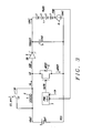
Fig. 3 HV WLED asynchronous boost converter with Coil Switch. -
Fig. 4 depicts a coil switch system of the present disclosure. -
Fig. 5 illustrates simulation results of the circuit disclosed, showing a typical case at room temperature. -
Fig. 6 illustrates a flowchart of a method disclosed to prevent ringing in Discontinuous Conduction Mode (DCM) of a boost converter for a white LED driver. - Methods and circuits for driving white LEDs (WLED) are disclosed. In a preferred embodiment a string of WLEDS is powered by the driver, e.g. for backlighting a display. LCD.
-
Fig. 1 shows a basic block diagram of a first embodiment of a high-voltage WLED boost converter disclosed. The circuit ofFig. 1 comprises a string ofexternal WLEDs 1 connected between an output voltage of a boost converter VBOOST and a node FBK, anexternal inductor L 2 connected between battery (VBAT) and node LX, an externalSchottky diode SD 3 connected between LX and the boosted voltage VBOOST, anexternal capacitor Cout 4 connected to the boosted voltage VBOOST, an integrated powerswitch NFET device 5 controlled by the signal GATE, an integrated programmablecurrent source IDAC 6 to bias the string of WLED 1, and an integrated regulation loop PWM_ctrl 7 with FBK (feedback) voltage as input and GATE signal as output. In the example ofFig. 1 a string of 4WLEDs 1 is shown, it should be noted that the instant disclosure applies also to one WLED or any number of WLEDs.
The main principle of operation and how regulation is achieved via modulating the width of pulses at the GATE (PWM) are noted here:- To supply a string of e.g. 4 or more WLEDs, the VBOOST voltage needs to be regulated at values equal to VBOOST = 4xVoltage_WLED + FBK > 10V, hence the integrated parts of the circuits exposed to these levels need to be implemented with High Voltage (HV) devices.
- The boost converter has two distinct modes of operation:
- 1. Discontinuous Conduction Mode (DCM), characterized by the current through the coil iL reaching zero when the NFET is off, unipolar diode current and average coil current iL_avg < iDAC;
- 2. Continuous Conduction Mode (CCM), characterized by iL always >0, bipolar diode current and average coil current iL_avg > iDAC.
-
Fig. 2 shows the signals in the boost converter during DCM:- During Ton the NFET 5 is on and
inductor L 2 is charged; - At the beginning of Toff, when the GATE signal turns off the NFET, the LX node flies above VBOOST and turn on the
diode SD 3 allowingL 2 to discharge intocapacitor Cout 4. - At the beginning of Tring, when iL reaches zero, the LX node starts to fall down. The inductance of
L 2 and the total capacitance at the LX node form a resonator making the LX node to oscillate potentially below VSS and causing the bulk diode in the NFET to conduct and chargeL 2. The ringing current iL during Tring is not transferred toWLED 1 but used to sustain the oscillation, which can hence be considered as dissipation.
- During Ton the NFET 5 is on and
-
Fig 3 shows the HV WLED asynchronous boost converter with aCoil Switch 30. To prevent the ringing, a common solution is to introduce a switch across thecoil CS 30 between the nodes VBAT and LX to virtually dump the oscillator when Tring occurs, while it remains open when the NFET is on. - The complications that the present invention intends to address are the following:
- The switching control signal CS_drv needs to be made available by design: in a synchronous boost converter the current sensing is not performed in the Toff phase (when the NFET is off) making the information of when iL reaches zero unavailable. A sensing of iL would require the use of an active device or resistor in series with L causing loss in efficiency equivalent to iLxRsense;
- The CS requires a fast turn on when the beginning Tring phase is detected: The LC constant can be quite small requiring a fast turn on of CS to stop the ringing: i.e. for L=10µH, C at LX=10pF, freq_LC∼16MHz;
- CS has to stand HV conditions (>10V);
- CS has to be a unipolar switch: during Ton no current must flow in CS, while during Tring CS has to be completely turned on. This represents a certain level of complication for the integrated technology in use for such WLED boost converter (HV BCD with enhancement C-MOS transistors).
-
Fig. 4 depicts acoil switch system 40 of the present disclosure. Thecoil switch system 40 comprises of three units: - The Coil Switch (CS) 41;
- The Edge Detector (ED) 42;
- The Boost Strap (BS) 43;
- The
coil switch CS 41 comprises 2 identical HV enhancement NMOS devices (N1 and N2) sharing the bulk connected to NMOS device N3. This arrangement allows to: - Isolate VBAT from LX when
CS 41 is off as the bulk diodes in N1 and N2 have the anodes not in series; - The bulk node is set to ground by N3 when
CS 41 is off and is set approximately to VBAT when CS turns on. A non-overlapping circuit (not shown) will prevent cross conduction between VBAT and VSS or VBOOST and VSS during transitions; - The signal "bulk_drv" becomes high when the signal GATE (see
Fig.1 ) becomes high and becomes low as soon as the edge detector activates the Coil Switch (seeFig. 5 ). A dedicate control logic prevents bulk_drv to become high when the Coil Switch is still on, avoiding shorts between battery and ground. - The
edge detector ED 42 comprises of asmall capacitor Csns 420 connected between LX and a HV current mirror of PMOS devices N6-N7: - When
CS 41 and NFET are both off (beginning of Toff),Csns 420 is charged to a voltage LX=VBOOST+V(SD3); - When LX falls down at the end of the discharging phase of
inductor L 2 into capacitor Cout 4 (beginning of Tring),capacitor Csns 420 discharges from LX pushing a current into the current mirror N6-N7 and triggering flip-flop FF which is kept in reset during the Ton phase. - Diode D2 clamps the upper plate of
capacitor Csns 420 slightly above VBOOST. - The boot-
strap BS 43 comprises an integrated capacitor Cp: - When the coil switch CS is off capacitor Cp is charged to VBAT via diode D1 while the bottom plate of capacitor Cp is held to VSS by
amplifier DRV 430. NMOS device N5 is on keeping the coil switch CS off and PMOS device N4 is off. - When CS is turned on, the bottom plate of capacitor Cp is charged to VBAT by
amplifier DRV 430. N5 is off and N4 on. The charge accumulated in Cp in the Ton phase is reversed into the gate capacitance of CS to a value close to 2xVBAT-Vdiode turning CS on. - The architecture presented has a very little DC operating current consumption (∼15µA typical) while during transients it is required to charge and discharge capacitor Cp in bootstrap circuit BS. While the boost is in CCM mode, the coil switch CS system can also be left activated as Cp will never perform the bootstrapping.
- It should be noted that
Fig. 4 illustrates some key points of the disclosure, namely: - A HV Coil Switch (CS), to short the coil of a boost converter when the current in it reaches zero during DCM, made of a series of 2 identical HV enhancement NMOS with bulk switch system;
- a HV Edge Detector (ED) to sense the fast falling edge of the LX node;
- a Boost Strap (BS) system to lift the gate of CS above the VBAT level and turn on CS;
- Minimum DC current required to operate to minimize impacts on efficiency;
- High Voltage (HV) devices are deployed to be compatible with the VBOOST levels;
"middle voltage" is compatible with the Battery (VBAT) levels.
InFig 3 NFET 5 is HV;
InFig. 4 N1, N2, N3, N4, N5, and N6 are HV. -
Fig. 5 illustrates simulation results of the circuit disclosed, showing a typical case at room temperature. The final plot shows the simulated results with and without the CS activated.
From the top to bottom (seeFig. 4 andFig. 5 for reference): - CS_drv 51 and
bulk_drv 50; -
ED output 52; -
GATE 54 -
LX 53; and - IL.55
- It should be noted that the architecture disclosed is scalable for different values of the inductor L and ESR (Equivalent Series Resistance). The size of N1 and N2 would require to be scaled to reach the desired On-resistance and the Cp capacitor scaled to compensate for the increased/decreased value of gate capacitance of the coil switch CS.
- It should also be noted that the coil switch, the edge detector, and the boot strap circuit disclosed here can be used together with the WLED driver as disclosed in the European patent application
12002094.6,. filed March 24, 2012 Fig. 4 of the present patent application toFig.1 of the patent application European application number12002094.6 - The CS can be used in any other backlight system without the improvements of the patent application European application number
12002094.6, filed March 24, 2012 -
Fig. 6 illustrates a flowchart of a method disclosed to prevent ringing in Discontinuous Conduction Mode (DCM) of a boost converter for a white LED driver.Step 60 of the method ofFig. 6 illustrates the provision of a high-voltage WLED asynchronous boost converter, driving one or more WLEDs connected in series, wherein the boost converter comprises a port for an input voltage, an inductor, a diode, a power switch, wherein the inductor, the diode, and the power switch are all connected to a LX node.Step 61 depicts sensing a fast falling edge of the voltage at the LX node in order to immediately initiate shorting the inductor if required.Step 62 illustrates shorting the inductor when the current through the inductor reaches zero during DCM mode by a coil switch across the inductor.Step 63 illustrates turning on the switch, if required, by lifting the gate of the switch above the input voltage level. - While the disclosure has been particularly shown and described with reference to the preferred embodiments thereof, it will be understood by those skilled in the art that various changes in form and details may be made without departing from the spirit and scope of the disclosure.
Claims (15)
- A method to prevent ringing in Discontinuous Conduction Mode (DCM) of a boost converter for a white LED driver, comprising the following steps:(1) providing a high-voltage WLED asynchronous boost converter, driving one or more WLEDs connected in series, wherein the boost converter comprises a port for an input voltage, an inductor, a diode, a power switch, wherein the inductor, the diode, and the power switch are all connected to a LX node;(2) sensing a fast falling edge of the voltage at the LX node in order to immediately initiate shorting the inductor if required;(3) shorting the inductor when the current through the inductor reaches zero during DCM mode by a coil switch across the inductor; and(4) turning on the switch, if required, by lifting the gate of the switch above the input voltage level.
- The method of claim 1 wherein said coil switch isolates the input voltage from the node LX when the coil switch is OFF.
- The method of claim 1 wherein the coil switch comprises two identical HV enhancement NMOS devices sharing a bulk, which is connected to an NMOS transistor N3.
- The method of claim 1 wherein the sensing of falling edge of the LX node is performed by an edge detector comprising a capacitor connected to the node LX, wherein said capacitor is charged to a voltage LX ≥VBOOST when both the coil switch and the power switch are OFF.
- The method of claim 1 wherein the turning ON the coil switch is performed by a boot-strap circuit comprising a capacitor Cp wherein the coil switch is turned ON by reversing a charge accumulated in capacitor Cp to a gate capacitance of the coil switch.
- The method of claim 5 wherein, when the coil switch is OFF, the capacitor Cp is charged to the input voltage via an integrated diode while a bottom plate is held to VSS voltage by an integrated driver.
- A circuit to prevent ringing in Discontinuous Conduction Mode (DCM) of a boost converter for a white LED driver, comprising:- a boost converter comprising:- a port for an input voltage;- an inductor connected between a first terminal of the port for the input voltage and a node LX, wherein a high voltage coil switch circuit is shorting the inductor when a current through the inductor reaches zero during DCM mode;- said high voltage switch circuit being controlled by a boot strap circuit;- a high voltage edge detector sensing a fast falling edge of the voltage at a LX node in order to immediately initiate shorting the inductor via a boot strap circuit, if required, wherein the LX node connects a second terminal of the inductor, a first rectifying means, and a power switch, and wherein the edge detector is connected via a first and a second connection to the boot strap circuit;- said boot strap circuit to lift a gate of the high voltage switch circuit above a level of the input voltage and to turn on the coil switch;- said first rectifying means connected between the node LX and an output voltage of the boost converter;- a first capacitive means connected between output ports of the boost converter;- said power switch connected between the node LX and VSS voltage, wherein the power switch is controlled by output signals of a PWM control unit; and- said PWM control units receiving inputs from a clock signal generator and from a voltage level from a node, connected between a second terminal of a programmable current source and a second terminal of one or more white LEDs connected in series;- said one or more white LEDs, wherein a first terminal of the one or more white LEDs is connected to a first output port of the boost converter; and- said programmable current source to deliver a bias current to the one or more white LEDs, wherein a first terminal of the current source is connected to VSS voltage.
- The circuit of claim 7 wherein said rectifying means is a Schottky diode.
- The circuit of claim 7 wherein said power switch is a NFET device.
- The circuit of claim 7 wherein said coil switch circuit comprises:- a first and second identical high voltage enhancement NMOS device, sharing a bulk, which is connected to a drain of a third NMOS device, wherein both gates are receiving input from a connected together to the boot strap circuit, the drain of the first NMOS device is connected to the input voltage, both sources are connected together, and the drain of the second NMOS device is connected to the LX node; and- said third NMOS device wherein the source is connected to VSS voltage and the gate is receiving a bulk_drv signal.
- The circuit of claim 7 wherein said edge detector comprises:- a sixth and a seventh NMOS device forming a current mirror, wherein both sources are connected to an output voltage of the boost converter, both gates and a drain of the fifth NMOS device are connected to a first terminal of a second capacitive means and to an anode of a second rectifying means, and the drain of the seventh transistor is connected to a first terminal of a current source and to a first terminal of a flip-flop;- said second capacitive means, wherein its second terminal is connected to LX node;- said second rectifying means wherein its cathode is connected to the output voltage of the boost converter;- said current source, wherein its second terminal is connected to the LX node;- said flip-flop, wherein a second terminal is connected to an input of an inverting amplifier and via the first connection to the bootstrap circuit; and- said inverting amplifier wherein an output is connected via the second connection to the boot strap circuit.
- The circuit of claim 7 wherein said boot strap circuit comprises:- a driver amplifier, wherein an input is the second connection to edge detector circuit and an output is connected to a first terminal of third capacitive means;- said third capacitive means, wherein a second terminal of the third capacitive means is connected to a cathode of a third rectifying means and to a bulk and to a source of a fourth PMOS transistor;- said third rectifying means wherein its anode is connected to the input voltage;- said fourth PMOS transistor, wherein a gate is connected to the second connection to the edge transistor and to a gate of a fifth NMOS transistor, and a drain is connected to a drain of the third transistor and is controlling the coil switch circuit; and- said fifth NMOS transistor wherein a source and a bulk is connected to VSS voltage.
- The circuit of claim 7 wherein said third capacitive means has an integrated capacitance of about 20pF and/or wherein said low voltage is in the order of magnitude of about 5V.
- A method to optimize efficiency and to prevent ringing in Discontinuous Conduction Mode (DCM) of a boost converter for a white LED driver, comprising the following steps:(1) providing a device comprising an arrangement of one or more white LEDs in series, a programmable iDAC current source, a high-voltage WLED asynchronous boost converter, driving the one or more WLEDs, wherein the boost converter comprises a port for an input voltage, an inductor, a diode, a power switch, and a programmable reference voltage generator for an error amplifier stage, wherein the inductor, the diode, and the power switch are all connected to a LX node;(2) sensing a fast falling edge of the voltage at the LX node in order to immediately initiate shorting the inductor if required;(3) shorting the inductor when the current through the inductor reaches zero during DCM mode by a coil switch across the inductor; and(4) turning on the switch, if required, by lifting the gate of the switch above the input voltage level.
- A circuit to prevent ringing of a white LED driver having optimized efficiency, comprising:- a boost converter comprising:- a port for an input voltage;- an inductor connected between a first terminal of the port for the input voltage and a node LX, wherein a high voltage coil switch circuit is shorting the inductor when a current through the inductor reaches zero during DCM mode;- said high voltage switch circuit being controlled by a boot strap circuit; a high voltage edge detector sensing a fast falling edge of the voltage at a LX node in order to immediately initiate shorting the inductor via a boot strap circuit, if required, wherein the LX node connects a second terminal of the inductor, a first rectifying means, and a power switch, and wherein the edge detector is connected via a first and a second connection to the boot strap circuit;- said boot strap circuit to lift a gate of the high voltage switch circuit above a level of the input voltage and to turn on the coil switch;- a rectifying means connected between the node LX and an output voltage of the boost converter;- a capacitor connected between output ports of the boost converter; said power switch connected between the node LX and a second terminal of a sense resistor, wherein the power switch is controlled by a signal from a regulation loop;- said sense resistor, wherein a second terminal of the sense resistor is connected to a second terminal of said port for the input voltage; and- said regulation loop connected between a second terminal of a programmable current source and a gate of said power switch;- said one or more white LEDs connected in series wherein a first terminal of the one or more white LEDs is connected to a first output port of the boost converter and a second terminal of the one or more white LEDs is connected to the second terminal of the programmable current source; and- said programmable current source to deliver a bias current to the one or more white LEDs, wherein a second terminal of the current source is connected to the second terminal of said port for the input voltage.
Priority Applications (2)
| Application Number | Priority Date | Filing Date | Title |
|---|---|---|---|
| EP12368008.4A EP2648483B1 (en) | 2012-04-06 | 2012-04-06 | Method of preventing spurious ringing during discontinuous conduction mode in inductive boost converters for white LED drivers |
| US13/443,914 US8933635B2 (en) | 2012-04-06 | 2012-04-11 | Method of preventing spurious ringing during discontinuous conduction mode in inductive boost converters for white LED drivers |
Applications Claiming Priority (1)
| Application Number | Priority Date | Filing Date | Title |
|---|---|---|---|
| EP12368008.4A EP2648483B1 (en) | 2012-04-06 | 2012-04-06 | Method of preventing spurious ringing during discontinuous conduction mode in inductive boost converters for white LED drivers |
Publications (2)
| Publication Number | Publication Date |
|---|---|
| EP2648483A1 true EP2648483A1 (en) | 2013-10-09 |
| EP2648483B1 EP2648483B1 (en) | 2019-08-07 |
Family
ID=46087620
Family Applications (1)
| Application Number | Title | Priority Date | Filing Date |
|---|---|---|---|
| EP12368008.4A Active EP2648483B1 (en) | 2012-04-06 | 2012-04-06 | Method of preventing spurious ringing during discontinuous conduction mode in inductive boost converters for white LED drivers |
Country Status (2)
| Country | Link |
|---|---|
| US (1) | US8933635B2 (en) |
| EP (1) | EP2648483B1 (en) |
Cited By (4)
| Publication number | Priority date | Publication date | Assignee | Title |
|---|---|---|---|---|
| CN104602396A (en) * | 2014-11-21 | 2015-05-06 | 深圳市海思半导体有限公司 | WLED (White Light Emitting Diode) driver and driving control method thereof |
| CN109450412A (en) * | 2016-05-03 | 2019-03-08 | 苏州泰思特电子科技有限公司 | High pressure damped oscillation generator |
| CN109889037A (en) * | 2017-12-06 | 2019-06-14 | 群光电能科技股份有限公司 | The circuit structure of the switching power supply |
| WO2023049115A1 (en) * | 2021-09-21 | 2023-03-30 | Ademco Inc. | Led switching power supply |
Families Citing this family (6)
| Publication number | Priority date | Publication date | Assignee | Title |
|---|---|---|---|---|
| US9171738B2 (en) | 2012-12-18 | 2015-10-27 | Infineon Technologies Austria Ag | Systems and methods for integrating bootstrap circuit elements in power transistors and other devices |
| JP6835082B2 (en) * | 2016-06-02 | 2021-02-24 | 日産自動車株式会社 | Power converter |
| GB2554904A (en) * | 2016-10-13 | 2018-04-18 | Chang Hsiutseng | Lighting apparatus |
| CN109256944B (en) * | 2018-10-17 | 2021-04-09 | 海宁开关厂有限公司 | Active disturbance rejection control method of Cuk converter |
| US10673337B1 (en) * | 2018-12-28 | 2020-06-02 | Texas Instruments Incorporated | Switched-mode DC/DC converter having a bootstrapped high-side driver |
| US10790747B1 (en) * | 2019-10-07 | 2020-09-29 | Analog Devices International Unlimited Company | Inductor current shunt for mitigation of load dump transients in DC-DC regulators |
Citations (6)
| Publication number | Priority date | Publication date | Assignee | Title |
|---|---|---|---|---|
| US5751139A (en) * | 1997-03-11 | 1998-05-12 | Unitrode Corporation | Multiplexing power converter |
| EP1200209A1 (en) | 1999-07-20 | 2002-05-02 | Danieli & C. Officine Meccaniche SpA | Rolling stand for plane products and method to control the planarity of said products |
| DE102004031395A1 (en) * | 2004-06-29 | 2006-02-02 | Infineon Technologies Ag | DC converter |
| US20080252273A1 (en) * | 2007-04-16 | 2008-10-16 | Jda Technology Co. Ltd. | Dc/dc converter |
| US20090010035A1 (en) * | 2007-07-06 | 2009-01-08 | Advanced Analogic Technologies, Inc. | Boost and up-down switching regulator with synchronous freewheeling MOSFET |
| US20090027027A1 (en) * | 2007-07-26 | 2009-01-29 | Shui-Mu Lin | Anti-ring asynchronous boost converter and anti-ring method for an asynchronous boost converter |
Family Cites Families (13)
| Publication number | Priority date | Publication date | Assignee | Title |
|---|---|---|---|---|
| US5550458A (en) | 1994-05-31 | 1996-08-27 | Lucent Technologies Inc. | Low-loss snubber for a power factor corrected boost converter |
| US6963178B1 (en) * | 1998-12-07 | 2005-11-08 | Systel Development And Industries Ltd. | Apparatus for controlling operation of gas discharge devices |
| US20050151518A1 (en) | 2004-01-08 | 2005-07-14 | Schneiker Henry D. | Regulated open-loop constant-power power supply |
| TWI344631B (en) * | 2006-11-13 | 2011-07-01 | Richtek Technology Corp | Backlight control circuit |
| US7579814B2 (en) | 2007-01-12 | 2009-08-25 | Potentia Semiconductor Corporation | Power converter with snubber |
| TWI337008B (en) | 2007-03-26 | 2011-02-01 | Richtek Technology Corp | Anti-ringing switching regulator and control method therefor |
| WO2009055821A1 (en) * | 2007-10-26 | 2009-04-30 | Lighting Science Group Corporation | High efficiency light source with integrated ballast |
| US8035314B2 (en) * | 2008-06-23 | 2011-10-11 | Freescale Semiconductor, Inc. | Method and device for LED channel managment in LED driver |
| US20100295472A1 (en) * | 2009-05-06 | 2010-11-25 | Polar Semiconductor, Inc. | Power supply for floating loads |
| US8305004B2 (en) * | 2009-06-09 | 2012-11-06 | Stmicroelectronics, Inc. | Apparatus and method for constant power offline LED driver |
| US8344657B2 (en) * | 2009-11-03 | 2013-01-01 | Intersil Americas Inc. | LED driver with open loop dimming control |
| US20110169416A1 (en) * | 2010-01-10 | 2011-07-14 | Wen-Hsiung Hsieh | Discontinuous current regulator circuit for driving light-emitting diodes |
| US8575856B2 (en) * | 2011-06-01 | 2013-11-05 | City University Of Hong Kong | Driver circuit for powering a DC lamp in a non-DC lamp fitting |
-
2012
- 2012-04-06 EP EP12368008.4A patent/EP2648483B1/en active Active
- 2012-04-11 US US13/443,914 patent/US8933635B2/en active Active
Patent Citations (6)
| Publication number | Priority date | Publication date | Assignee | Title |
|---|---|---|---|---|
| US5751139A (en) * | 1997-03-11 | 1998-05-12 | Unitrode Corporation | Multiplexing power converter |
| EP1200209A1 (en) | 1999-07-20 | 2002-05-02 | Danieli & C. Officine Meccaniche SpA | Rolling stand for plane products and method to control the planarity of said products |
| DE102004031395A1 (en) * | 2004-06-29 | 2006-02-02 | Infineon Technologies Ag | DC converter |
| US20080252273A1 (en) * | 2007-04-16 | 2008-10-16 | Jda Technology Co. Ltd. | Dc/dc converter |
| US20090010035A1 (en) * | 2007-07-06 | 2009-01-08 | Advanced Analogic Technologies, Inc. | Boost and up-down switching regulator with synchronous freewheeling MOSFET |
| US20090027027A1 (en) * | 2007-07-26 | 2009-01-29 | Shui-Mu Lin | Anti-ring asynchronous boost converter and anti-ring method for an asynchronous boost converter |
Cited By (6)
| Publication number | Priority date | Publication date | Assignee | Title |
|---|---|---|---|---|
| CN104602396A (en) * | 2014-11-21 | 2015-05-06 | 深圳市海思半导体有限公司 | WLED (White Light Emitting Diode) driver and driving control method thereof |
| US9622305B2 (en) | 2014-11-21 | 2017-04-11 | Huawei Technologies Co., Ltd. | WLED driver and drive control method |
| CN109450412A (en) * | 2016-05-03 | 2019-03-08 | 苏州泰思特电子科技有限公司 | High pressure damped oscillation generator |
| CN109889037A (en) * | 2017-12-06 | 2019-06-14 | 群光电能科技股份有限公司 | The circuit structure of the switching power supply |
| WO2023049115A1 (en) * | 2021-09-21 | 2023-03-30 | Ademco Inc. | Led switching power supply |
| US12610439B2 (en) | 2021-09-21 | 2026-04-21 | Resideo Llc | LED switching power supply |
Also Published As
| Publication number | Publication date |
|---|---|
| EP2648483B1 (en) | 2019-08-07 |
| US8933635B2 (en) | 2015-01-13 |
| US20130264953A1 (en) | 2013-10-10 |
Similar Documents
| Publication | Publication Date | Title |
|---|---|---|
| US8933635B2 (en) | Method of preventing spurious ringing during discontinuous conduction mode in inductive boost converters for white LED drivers | |
| US7737767B2 (en) | Control circuit and control method for charge pump circuit | |
| CN101500360B (en) | Direct-current power supply device, power supply device for driving LED and semiconductor integrated circuit for controlling power supply | |
| EP3205008B1 (en) | Shared bootstrap capacitor for multiple phase buck converter circuit and methods | |
| JP5744871B2 (en) | High efficiency stabilized charge pump | |
| EP2642823B1 (en) | Method for optimizing efficiency versus load current in an inductive boost converter for white LED driving | |
| US8970575B2 (en) | Power source circuit and liquid crystal display apparatus having the same | |
| US20100127672A1 (en) | Power Supply Device with Fast Output Voltage Switching Capability | |
| US10504434B2 (en) | DC-DC converter and display device having the same | |
| CN107947576B (en) | Low buck switching power supply with reduced switching losses | |
| US11645983B2 (en) | Booster circuit and driving method thereof, backlight module and display device | |
| TWI740203B (en) | Gate driving circuit, charge pump having the same, and chip | |
| JP2009177906A (en) | Charge pump circuit | |
| US20060267671A1 (en) | Charge pump circuit for high side drive circuit and driver driving voltage circuit | |
| US7551004B2 (en) | Inverter apparatus with improved gate drive for power MOSFET | |
| US20120098441A1 (en) | LED Driving System and Driving Method Thereof | |
| US20170243534A1 (en) | Power supply circuit, driving method for the same and display device | |
| CN101111987A (en) | Step-up/step-down regulator circuit and liquid crystal display device incorporating the same | |
| US7362163B1 (en) | Flyback capacitor level shifter feedback regulation for negative pumps | |
| US11025162B2 (en) | Charge pump systems, devices, and methods | |
| US7531966B2 (en) | Lamp ballast circuit | |
| US20120105035A1 (en) | Buck Circuit Having Fast Transient Response Mechanism and Operation of the Same | |
| TWI484743B (en) | Boost circuit driven by low voltage and associated method | |
| US9413340B1 (en) | DC-to-DC voltage converter using switching frequency detection | |
| KR100696563B1 (en) | Power supply |
Legal Events
| Date | Code | Title | Description |
|---|---|---|---|
| PUAI | Public reference made under article 153(3) epc to a published international application that has entered the european phase |
Free format text: ORIGINAL CODE: 0009012 |
|
| AK | Designated contracting states |
Kind code of ref document: A1 Designated state(s): AL AT BE BG CH CY CZ DE DK EE ES FI FR GB GR HR HU IE IS IT LI LT LU LV MC MK MT NL NO PL PT RO RS SE SI SK SM TR |
|
| AX | Request for extension of the european patent |
Extension state: BA ME |
|
| 17P | Request for examination filed |
Effective date: 20140328 |
|
| RBV | Designated contracting states (corrected) |
Designated state(s): AL AT BE BG CH CY CZ DE DK EE ES FI FR GB GR HR HU IE IS IT LI LT LU LV MC MK MT NL NO PL PT RO RS SE SI SK SM TR |
|
| STAA | Information on the status of an ep patent application or granted ep patent |
Free format text: STATUS: EXAMINATION IS IN PROGRESS |
|
| 17Q | First examination report despatched |
Effective date: 20180208 |
|
| GRAP | Despatch of communication of intention to grant a patent |
Free format text: ORIGINAL CODE: EPIDOSNIGR1 |
|
| STAA | Information on the status of an ep patent application or granted ep patent |
Free format text: STATUS: GRANT OF PATENT IS INTENDED |
|
| INTG | Intention to grant announced |
Effective date: 20190220 |
|
| GRAS | Grant fee paid |
Free format text: ORIGINAL CODE: EPIDOSNIGR3 |
|
| GRAA | (expected) grant |
Free format text: ORIGINAL CODE: 0009210 |
|
| STAA | Information on the status of an ep patent application or granted ep patent |
Free format text: STATUS: THE PATENT HAS BEEN GRANTED |
|
| AK | Designated contracting states |
Kind code of ref document: B1 Designated state(s): AL AT BE BG CH CY CZ DE DK EE ES FI FR GB GR HR HU IE IS IT LI LT LU LV MC MK MT NL NO PL PT RO RS SE SI SK SM TR |
|
| REG | Reference to a national code |
Ref country code: GB Ref legal event code: FG4D |
|
| REG | Reference to a national code |
Ref country code: CH Ref legal event code: EP Ref country code: AT Ref legal event code: REF Ref document number: 1165869 Country of ref document: AT Kind code of ref document: T Effective date: 20190815 |
|
| REG | Reference to a national code |
Ref country code: DE Ref legal event code: R096 Ref document number: 602012062644 Country of ref document: DE |
|
| REG | Reference to a national code |
Ref country code: IE Ref legal event code: FG4D |
|
| REG | Reference to a national code |
Ref country code: DE Ref legal event code: R079 Ref document number: 602012062644 Country of ref document: DE Free format text: PREVIOUS MAIN CLASS: H05B0033080000 Ipc: H05B0045000000 |
|
| REG | Reference to a national code |
Ref country code: NL Ref legal event code: MP Effective date: 20190807 |
|
| REG | Reference to a national code |
Ref country code: LT Ref legal event code: MG4D |
|
| PG25 | Lapsed in a contracting state [announced via postgrant information from national office to epo] |
Ref country code: NO Free format text: LAPSE BECAUSE OF FAILURE TO SUBMIT A TRANSLATION OF THE DESCRIPTION OR TO PAY THE FEE WITHIN THE PRESCRIBED TIME-LIMIT Effective date: 20191107 Ref country code: HR Free format text: LAPSE BECAUSE OF FAILURE TO SUBMIT A TRANSLATION OF THE DESCRIPTION OR TO PAY THE FEE WITHIN THE PRESCRIBED TIME-LIMIT Effective date: 20190807 Ref country code: SE Free format text: LAPSE BECAUSE OF FAILURE TO SUBMIT A TRANSLATION OF THE DESCRIPTION OR TO PAY THE FEE WITHIN THE PRESCRIBED TIME-LIMIT Effective date: 20190807 Ref country code: BG Free format text: LAPSE BECAUSE OF FAILURE TO SUBMIT A TRANSLATION OF THE DESCRIPTION OR TO PAY THE FEE WITHIN THE PRESCRIBED TIME-LIMIT Effective date: 20191107 Ref country code: NL Free format text: LAPSE BECAUSE OF FAILURE TO SUBMIT A TRANSLATION OF THE DESCRIPTION OR TO PAY THE FEE WITHIN THE PRESCRIBED TIME-LIMIT Effective date: 20190807 Ref country code: LT Free format text: LAPSE BECAUSE OF FAILURE TO SUBMIT A TRANSLATION OF THE DESCRIPTION OR TO PAY THE FEE WITHIN THE PRESCRIBED TIME-LIMIT Effective date: 20190807 Ref country code: FI Free format text: LAPSE BECAUSE OF FAILURE TO SUBMIT A TRANSLATION OF THE DESCRIPTION OR TO PAY THE FEE WITHIN THE PRESCRIBED TIME-LIMIT Effective date: 20190807 Ref country code: PT Free format text: LAPSE BECAUSE OF FAILURE TO SUBMIT A TRANSLATION OF THE DESCRIPTION OR TO PAY THE FEE WITHIN THE PRESCRIBED TIME-LIMIT Effective date: 20191209 |
|
| REG | Reference to a national code |
Ref country code: AT Ref legal event code: MK05 Ref document number: 1165869 Country of ref document: AT Kind code of ref document: T Effective date: 20190807 |
|
| PG25 | Lapsed in a contracting state [announced via postgrant information from national office to epo] |
Ref country code: AL Free format text: LAPSE BECAUSE OF FAILURE TO SUBMIT A TRANSLATION OF THE DESCRIPTION OR TO PAY THE FEE WITHIN THE PRESCRIBED TIME-LIMIT Effective date: 20190807 Ref country code: RS Free format text: LAPSE BECAUSE OF FAILURE TO SUBMIT A TRANSLATION OF THE DESCRIPTION OR TO PAY THE FEE WITHIN THE PRESCRIBED TIME-LIMIT Effective date: 20190807 Ref country code: GR Free format text: LAPSE BECAUSE OF FAILURE TO SUBMIT A TRANSLATION OF THE DESCRIPTION OR TO PAY THE FEE WITHIN THE PRESCRIBED TIME-LIMIT Effective date: 20191108 Ref country code: IS Free format text: LAPSE BECAUSE OF FAILURE TO SUBMIT A TRANSLATION OF THE DESCRIPTION OR TO PAY THE FEE WITHIN THE PRESCRIBED TIME-LIMIT Effective date: 20191207 Ref country code: LV Free format text: LAPSE BECAUSE OF FAILURE TO SUBMIT A TRANSLATION OF THE DESCRIPTION OR TO PAY THE FEE WITHIN THE PRESCRIBED TIME-LIMIT Effective date: 20190807 Ref country code: ES Free format text: LAPSE BECAUSE OF FAILURE TO SUBMIT A TRANSLATION OF THE DESCRIPTION OR TO PAY THE FEE WITHIN THE PRESCRIBED TIME-LIMIT Effective date: 20190807 |
|
| PG25 | Lapsed in a contracting state [announced via postgrant information from national office to epo] |
Ref country code: TR Free format text: LAPSE BECAUSE OF FAILURE TO SUBMIT A TRANSLATION OF THE DESCRIPTION OR TO PAY THE FEE WITHIN THE PRESCRIBED TIME-LIMIT Effective date: 20190807 |
|
| PG25 | Lapsed in a contracting state [announced via postgrant information from national office to epo] |
Ref country code: RO Free format text: LAPSE BECAUSE OF FAILURE TO SUBMIT A TRANSLATION OF THE DESCRIPTION OR TO PAY THE FEE WITHIN THE PRESCRIBED TIME-LIMIT Effective date: 20190807 Ref country code: IT Free format text: LAPSE BECAUSE OF FAILURE TO SUBMIT A TRANSLATION OF THE DESCRIPTION OR TO PAY THE FEE WITHIN THE PRESCRIBED TIME-LIMIT Effective date: 20190807 Ref country code: DK Free format text: LAPSE BECAUSE OF FAILURE TO SUBMIT A TRANSLATION OF THE DESCRIPTION OR TO PAY THE FEE WITHIN THE PRESCRIBED TIME-LIMIT Effective date: 20190807 Ref country code: PL Free format text: LAPSE BECAUSE OF FAILURE TO SUBMIT A TRANSLATION OF THE DESCRIPTION OR TO PAY THE FEE WITHIN THE PRESCRIBED TIME-LIMIT Effective date: 20190807 Ref country code: AT Free format text: LAPSE BECAUSE OF FAILURE TO SUBMIT A TRANSLATION OF THE DESCRIPTION OR TO PAY THE FEE WITHIN THE PRESCRIBED TIME-LIMIT Effective date: 20190807 Ref country code: EE Free format text: LAPSE BECAUSE OF FAILURE TO SUBMIT A TRANSLATION OF THE DESCRIPTION OR TO PAY THE FEE WITHIN THE PRESCRIBED TIME-LIMIT Effective date: 20190807 |
|
| PG25 | Lapsed in a contracting state [announced via postgrant information from national office to epo] |
Ref country code: CZ Free format text: LAPSE BECAUSE OF FAILURE TO SUBMIT A TRANSLATION OF THE DESCRIPTION OR TO PAY THE FEE WITHIN THE PRESCRIBED TIME-LIMIT Effective date: 20190807 Ref country code: SK Free format text: LAPSE BECAUSE OF FAILURE TO SUBMIT A TRANSLATION OF THE DESCRIPTION OR TO PAY THE FEE WITHIN THE PRESCRIBED TIME-LIMIT Effective date: 20190807 Ref country code: IS Free format text: LAPSE BECAUSE OF FAILURE TO SUBMIT A TRANSLATION OF THE DESCRIPTION OR TO PAY THE FEE WITHIN THE PRESCRIBED TIME-LIMIT Effective date: 20200224 Ref country code: SM Free format text: LAPSE BECAUSE OF FAILURE TO SUBMIT A TRANSLATION OF THE DESCRIPTION OR TO PAY THE FEE WITHIN THE PRESCRIBED TIME-LIMIT Effective date: 20190807 |
|
| REG | Reference to a national code |
Ref country code: DE Ref legal event code: R097 Ref document number: 602012062644 Country of ref document: DE |
|
| PLBE | No opposition filed within time limit |
Free format text: ORIGINAL CODE: 0009261 |
|
| STAA | Information on the status of an ep patent application or granted ep patent |
Free format text: STATUS: NO OPPOSITION FILED WITHIN TIME LIMIT |
|
| PG2D | Information on lapse in contracting state deleted |
Ref country code: IS |
|
| 26N | No opposition filed |
Effective date: 20200603 |
|
| PG25 | Lapsed in a contracting state [announced via postgrant information from national office to epo] |
Ref country code: SI Free format text: LAPSE BECAUSE OF FAILURE TO SUBMIT A TRANSLATION OF THE DESCRIPTION OR TO PAY THE FEE WITHIN THE PRESCRIBED TIME-LIMIT Effective date: 20190807 |
|
| PG25 | Lapsed in a contracting state [announced via postgrant information from national office to epo] |
Ref country code: MC Free format text: LAPSE BECAUSE OF FAILURE TO SUBMIT A TRANSLATION OF THE DESCRIPTION OR TO PAY THE FEE WITHIN THE PRESCRIBED TIME-LIMIT Effective date: 20190807 |
|
| REG | Reference to a national code |
Ref country code: CH Ref legal event code: PL |
|
| PG25 | Lapsed in a contracting state [announced via postgrant information from national office to epo] |
Ref country code: LU Free format text: LAPSE BECAUSE OF NON-PAYMENT OF DUE FEES Effective date: 20200406 Ref country code: CH Free format text: LAPSE BECAUSE OF NON-PAYMENT OF DUE FEES Effective date: 20200430 Ref country code: FR Free format text: LAPSE BECAUSE OF NON-PAYMENT OF DUE FEES Effective date: 20200430 Ref country code: LI Free format text: LAPSE BECAUSE OF NON-PAYMENT OF DUE FEES Effective date: 20200430 |
|
| REG | Reference to a national code |
Ref country code: BE Ref legal event code: MM Effective date: 20200430 |
|
| PG25 | Lapsed in a contracting state [announced via postgrant information from national office to epo] |
Ref country code: BE Free format text: LAPSE BECAUSE OF NON-PAYMENT OF DUE FEES Effective date: 20200430 |
|
| PG25 | Lapsed in a contracting state [announced via postgrant information from national office to epo] |
Ref country code: IE Free format text: LAPSE BECAUSE OF NON-PAYMENT OF DUE FEES Effective date: 20200406 |
|
| PG25 | Lapsed in a contracting state [announced via postgrant information from national office to epo] |
Ref country code: MT Free format text: LAPSE BECAUSE OF FAILURE TO SUBMIT A TRANSLATION OF THE DESCRIPTION OR TO PAY THE FEE WITHIN THE PRESCRIBED TIME-LIMIT Effective date: 20190807 Ref country code: CY Free format text: LAPSE BECAUSE OF FAILURE TO SUBMIT A TRANSLATION OF THE DESCRIPTION OR TO PAY THE FEE WITHIN THE PRESCRIBED TIME-LIMIT Effective date: 20190807 |
|
| PG25 | Lapsed in a contracting state [announced via postgrant information from national office to epo] |
Ref country code: MK Free format text: LAPSE BECAUSE OF FAILURE TO SUBMIT A TRANSLATION OF THE DESCRIPTION OR TO PAY THE FEE WITHIN THE PRESCRIBED TIME-LIMIT Effective date: 20190807 |
|
| PGFP | Annual fee paid to national office [announced via postgrant information from national office to epo] |
Ref country code: DE Payment date: 20250402 Year of fee payment: 14 |
|
| PGFP | Annual fee paid to national office [announced via postgrant information from national office to epo] |
Ref country code: GB Payment date: 20250411 Year of fee payment: 14 |