EP2646523B1 - Red emitting luminescent materials - Google Patents
Red emitting luminescent materials Download PDFInfo
- Publication number
- EP2646523B1 EP2646523B1 EP11797150.7A EP11797150A EP2646523B1 EP 2646523 B1 EP2646523 B1 EP 2646523B1 EP 11797150 A EP11797150 A EP 11797150A EP 2646523 B1 EP2646523 B1 EP 2646523B1
- Authority
- EP
- European Patent Office
- Prior art keywords
- systems
- lighting
- lighting systems
- materials
- present
- Prior art date
- Legal status (The legal status is an assumption and is not a legal conclusion. Google has not performed a legal analysis and makes no representation as to the accuracy of the status listed.)
- Active
Links
- 239000000463 material Substances 0.000 title claims description 64
- 239000002245 particle Substances 0.000 claims description 19
- 238000009826 distribution Methods 0.000 claims description 5
- 239000011575 calcium Substances 0.000 description 15
- 230000000052 comparative effect Effects 0.000 description 14
- OAICVXFJPJFONN-UHFFFAOYSA-N Phosphorus Chemical compound [P] OAICVXFJPJFONN-UHFFFAOYSA-N 0.000 description 13
- OYPRJOBELJOOCE-UHFFFAOYSA-N Calcium Chemical compound [Ca] OYPRJOBELJOOCE-UHFFFAOYSA-N 0.000 description 8
- 229910052791 calcium Inorganic materials 0.000 description 8
- 239000000203 mixture Substances 0.000 description 7
- 238000000034 method Methods 0.000 description 6
- 230000004907 flux Effects 0.000 description 5
- 239000000843 powder Substances 0.000 description 5
- 230000008901 benefit Effects 0.000 description 4
- 230000007423 decrease Effects 0.000 description 3
- 238000009877 rendering Methods 0.000 description 3
- NLXLAEXVIDQMFP-UHFFFAOYSA-N Ammonia chloride Chemical compound [NH4+].[Cl-] NLXLAEXVIDQMFP-UHFFFAOYSA-N 0.000 description 2
- KFZMGEQAYNKOFK-UHFFFAOYSA-N Isopropanol Chemical compound CC(C)O KFZMGEQAYNKOFK-UHFFFAOYSA-N 0.000 description 2
- 229910019142 PO4 Inorganic materials 0.000 description 2
- 229910052581 Si3N4 Inorganic materials 0.000 description 2
- VYPSYNLAJGMNEJ-UHFFFAOYSA-N Silicium dioxide Chemical compound O=[Si]=O VYPSYNLAJGMNEJ-UHFFFAOYSA-N 0.000 description 2
- 239000000654 additive Substances 0.000 description 2
- 238000000149 argon plasma sintering Methods 0.000 description 2
- QVGXLLKOCUKJST-UHFFFAOYSA-N atomic oxygen Chemical compound [O] QVGXLLKOCUKJST-UHFFFAOYSA-N 0.000 description 2
- 238000000498 ball milling Methods 0.000 description 2
- 238000006243 chemical reaction Methods 0.000 description 2
- 238000000295 emission spectrum Methods 0.000 description 2
- 230000036571 hydration Effects 0.000 description 2
- 238000006703 hydration reaction Methods 0.000 description 2
- 238000004519 manufacturing process Methods 0.000 description 2
- 230000003287 optical effect Effects 0.000 description 2
- 229910052760 oxygen Inorganic materials 0.000 description 2
- 239000001301 oxygen Substances 0.000 description 2
- 235000021317 phosphate Nutrition 0.000 description 2
- 150000003013 phosphoric acid derivatives Chemical class 0.000 description 2
- 239000002096 quantum dot Substances 0.000 description 2
- XLYOFNOQVPJJNP-UHFFFAOYSA-N water Substances O XLYOFNOQVPJJNP-UHFFFAOYSA-N 0.000 description 2
- OKTJSMMVPCPJKN-UHFFFAOYSA-N Carbon Chemical compound [C] OKTJSMMVPCPJKN-UHFFFAOYSA-N 0.000 description 1
- ZOKXTWBITQBERF-UHFFFAOYSA-N Molybdenum Chemical compound [Mo] ZOKXTWBITQBERF-UHFFFAOYSA-N 0.000 description 1
- 230000003213 activating effect Effects 0.000 description 1
- 150000004645 aluminates Chemical class 0.000 description 1
- 235000019270 ammonium chloride Nutrition 0.000 description 1
- 229910052586 apatite Inorganic materials 0.000 description 1
- 229910052788 barium Inorganic materials 0.000 description 1
- DSAJWYNOEDNPEQ-UHFFFAOYSA-N barium atom Chemical compound [Ba] DSAJWYNOEDNPEQ-UHFFFAOYSA-N 0.000 description 1
- 230000005540 biological transmission Effects 0.000 description 1
- 150000001642 boronic acid derivatives Chemical class 0.000 description 1
- 229910052799 carbon Inorganic materials 0.000 description 1
- 230000008859 change Effects 0.000 description 1
- 229910052681 coesite Inorganic materials 0.000 description 1
- 229910052906 cristobalite Inorganic materials 0.000 description 1
- 230000007812 deficiency Effects 0.000 description 1
- 230000001419 dependent effect Effects 0.000 description 1
- 238000011161 development Methods 0.000 description 1
- 239000010432 diamond Substances 0.000 description 1
- 239000002270 dispersing agent Substances 0.000 description 1
- 238000001035 drying Methods 0.000 description 1
- 230000000694 effects Effects 0.000 description 1
- RSEIMSPAXMNYFJ-UHFFFAOYSA-N europium(III) oxide Inorganic materials O=[Eu]O[Eu]=O RSEIMSPAXMNYFJ-UHFFFAOYSA-N 0.000 description 1
- 238000010304 firing Methods 0.000 description 1
- 150000002222 fluorine compounds Chemical class 0.000 description 1
- 239000008187 granular material Substances 0.000 description 1
- 150000004820 halides Chemical class 0.000 description 1
- 239000012535 impurity Substances 0.000 description 1
- 239000007788 liquid Substances 0.000 description 1
- 238000004020 luminiscence type Methods 0.000 description 1
- 238000005259 measurement Methods 0.000 description 1
- 229910021645 metal ion Inorganic materials 0.000 description 1
- 229910044991 metal oxide Inorganic materials 0.000 description 1
- 238000012986 modification Methods 0.000 description 1
- 230000004048 modification Effects 0.000 description 1
- 229910052750 molybdenum Inorganic materials 0.000 description 1
- 239000011733 molybdenum Substances 0.000 description 1
- 239000012299 nitrogen atmosphere Substances 0.000 description 1
- 125000004433 nitrogen atom Chemical group N* 0.000 description 1
- 125000004430 oxygen atom Chemical group O* 0.000 description 1
- 238000011192 particle characterization Methods 0.000 description 1
- VSIIXMUUUJUKCM-UHFFFAOYSA-D pentacalcium;fluoride;triphosphate Chemical compound [F-].[Ca+2].[Ca+2].[Ca+2].[Ca+2].[Ca+2].[O-]P([O-])([O-])=O.[O-]P([O-])([O-])=O.[O-]P([O-])([O-])=O VSIIXMUUUJUKCM-UHFFFAOYSA-D 0.000 description 1
- 230000010287 polarization Effects 0.000 description 1
- 238000002360 preparation method Methods 0.000 description 1
- 238000012545 processing Methods 0.000 description 1
- 229910052761 rare earth metal Inorganic materials 0.000 description 1
- 150000002910 rare earth metals Chemical class 0.000 description 1
- 238000012216 screening Methods 0.000 description 1
- 150000004760 silicates Chemical class 0.000 description 1
- 239000000377 silicon dioxide Substances 0.000 description 1
- HQVNEWCFYHHQES-UHFFFAOYSA-N silicon nitride Chemical compound N12[Si]34N5[Si]62N3[Si]51N64 HQVNEWCFYHHQES-UHFFFAOYSA-N 0.000 description 1
- 229910052682 stishovite Inorganic materials 0.000 description 1
- 238000006467 substitution reaction Methods 0.000 description 1
- 239000000725 suspension Substances 0.000 description 1
- 229910052723 transition metal Inorganic materials 0.000 description 1
- 150000003624 transition metals Chemical class 0.000 description 1
- 229910052905 tridymite Inorganic materials 0.000 description 1
- 238000005406 washing Methods 0.000 description 1
Images

Classifications
-
- C—CHEMISTRY; METALLURGY
- C09—DYES; PAINTS; POLISHES; NATURAL RESINS; ADHESIVES; COMPOSITIONS NOT OTHERWISE PROVIDED FOR; APPLICATIONS OF MATERIALS NOT OTHERWISE PROVIDED FOR
- C09K—MATERIALS FOR MISCELLANEOUS APPLICATIONS, NOT PROVIDED FOR ELSEWHERE
- C09K11/00—Luminescent, e.g. electroluminescent, chemiluminescent materials
- C09K11/08—Luminescent, e.g. electroluminescent, chemiluminescent materials containing inorganic luminescent materials
- C09K11/0883—Arsenides; Nitrides; Phosphides
-
- C—CHEMISTRY; METALLURGY
- C09—DYES; PAINTS; POLISHES; NATURAL RESINS; ADHESIVES; COMPOSITIONS NOT OTHERWISE PROVIDED FOR; APPLICATIONS OF MATERIALS NOT OTHERWISE PROVIDED FOR
- C09K—MATERIALS FOR MISCELLANEOUS APPLICATIONS, NOT PROVIDED FOR ELSEWHERE
- C09K11/00—Luminescent, e.g. electroluminescent, chemiluminescent materials
- C09K11/08—Luminescent, e.g. electroluminescent, chemiluminescent materials containing inorganic luminescent materials
- C09K11/64—Luminescent, e.g. electroluminescent, chemiluminescent materials containing inorganic luminescent materials containing aluminium
-
- C—CHEMISTRY; METALLURGY
- C09—DYES; PAINTS; POLISHES; NATURAL RESINS; ADHESIVES; COMPOSITIONS NOT OTHERWISE PROVIDED FOR; APPLICATIONS OF MATERIALS NOT OTHERWISE PROVIDED FOR
- C09K—MATERIALS FOR MISCELLANEOUS APPLICATIONS, NOT PROVIDED FOR ELSEWHERE
- C09K11/00—Luminescent, e.g. electroluminescent, chemiluminescent materials
- C09K11/08—Luminescent, e.g. electroluminescent, chemiluminescent materials containing inorganic luminescent materials
- C09K11/77—Luminescent, e.g. electroluminescent, chemiluminescent materials containing inorganic luminescent materials containing rare earth metals
- C09K11/7728—Luminescent, e.g. electroluminescent, chemiluminescent materials containing inorganic luminescent materials containing rare earth metals containing europium
- C09K11/77348—Silicon Aluminium Nitrides or Silicon Aluminium Oxynitrides
-
- F—MECHANICAL ENGINEERING; LIGHTING; HEATING; WEAPONS; BLASTING
- F21—LIGHTING
- F21V—FUNCTIONAL FEATURES OR DETAILS OF LIGHTING DEVICES OR SYSTEMS THEREOF; STRUCTURAL COMBINATIONS OF LIGHTING DEVICES WITH OTHER ARTICLES, NOT OTHERWISE PROVIDED FOR
- F21V9/00—Elements for modifying spectral properties, polarisation or intensity of the light emitted, e.g. filters
- F21V9/30—Elements containing photoluminescent material distinct from or spaced from the light source
-
- H—ELECTRICITY
- H01—ELECTRIC ELEMENTS
- H01L—SEMICONDUCTOR DEVICES NOT COVERED BY CLASS H10
- H01L33/00—Semiconductor devices with at least one potential-jump barrier or surface barrier specially adapted for light emission; Processes or apparatus specially adapted for the manufacture or treatment thereof or of parts thereof; Details thereof
- H01L33/02—Semiconductor devices with at least one potential-jump barrier or surface barrier specially adapted for light emission; Processes or apparatus specially adapted for the manufacture or treatment thereof or of parts thereof; Details thereof characterised by the semiconductor bodies
- H01L33/26—Materials of the light emitting region
-
- H—ELECTRICITY
- H01—ELECTRIC ELEMENTS
- H01L—SEMICONDUCTOR DEVICES NOT COVERED BY CLASS H10
- H01L33/00—Semiconductor devices with at least one potential-jump barrier or surface barrier specially adapted for light emission; Processes or apparatus specially adapted for the manufacture or treatment thereof or of parts thereof; Details thereof
- H01L33/48—Semiconductor devices with at least one potential-jump barrier or surface barrier specially adapted for light emission; Processes or apparatus specially adapted for the manufacture or treatment thereof or of parts thereof; Details thereof characterised by the semiconductor body packages
- H01L33/50—Wavelength conversion elements
- H01L33/501—Wavelength conversion elements characterised by the materials, e.g. binder
- H01L33/502—Wavelength conversion materials
-
- Y—GENERAL TAGGING OF NEW TECHNOLOGICAL DEVELOPMENTS; GENERAL TAGGING OF CROSS-SECTIONAL TECHNOLOGIES SPANNING OVER SEVERAL SECTIONS OF THE IPC; TECHNICAL SUBJECTS COVERED BY FORMER USPC CROSS-REFERENCE ART COLLECTIONS [XRACs] AND DIGESTS
- Y02—TECHNOLOGIES OR APPLICATIONS FOR MITIGATION OR ADAPTATION AGAINST CLIMATE CHANGE
- Y02B—CLIMATE CHANGE MITIGATION TECHNOLOGIES RELATED TO BUILDINGS, e.g. HOUSING, HOUSE APPLIANCES OR RELATED END-USER APPLICATIONS
- Y02B20/00—Energy efficient lighting technologies, e.g. halogen lamps or gas discharge lamps
Definitions
- the present invention is directed to novel luminescent materials for light emitting devices, especially to the field of novel luminescent materials for LEDs.
- Phosphors comprising silicates, phosphates (for example, apatite) and aluminates as host materials, with transition metals or rare earth metals added as activating materials to the host materials, are widely known.
- phosphates for example, apatite
- aluminates as host materials, with transition metals or rare earth metals added as activating materials to the host materials.
- transition metals or rare earth metals added as activating materials to the host materials
- US2010/289044 describes a white light LED that uses an LED die that emits visible blue light in a wavelength range of about 450-470 nm.
- a red phosphor or quantum dot material converts some of the blue light to a visible red light having a peak wavelength between about 605-625 nm with a full-width-half-maximum (FWHM) less than 80 nm.
- a green phosphor or quantum dot material converts some of the blue light to a green light having a FWHM greater than 40 nm, wherein the combination of the blue light, red light, and green light produces a white light providing a color rendering of Ra,8>90 and a color temperature of between 2500K-5000K.
- the red and green converting material do not saturate with an LED die output of 100 W/cm 2 and can reliably operate with an LED die junction temperature over 100 degrees C.
- a material according to claim 1 of the present invention Accordingly, a material (Ba 1-x-y-z Sr x Ca y Eu 2 ) 2 Si 5-a-b Al a N 8-a-4b O a+4b having an average particle size distribution d 50 of ⁇ 6 ⁇ m is provided, whereby 0.3 ⁇ x ⁇ 0.9, 0.01 ⁇ y ⁇ 0.1, 0.005 ⁇ z ⁇ 0.04,0 ⁇ a ⁇ 0.2 and 0 ⁇ b ⁇ 0.2, as further defined in the accompanying claims.
- additives may also be present in the bulk compositions. These additives particularly include such species known to the art as fluxes. Suitable fluxes include alkaline earth - or alkaline - metal oxides, borates, phosphates and halides such as fluorides, ammonium chloride, SiO 2 and the like and mixtures thereof
- this invention also relates to the use of calcium in siliconitridic materials for increasing the average particle size.
- 0.35 ⁇ x ⁇ 0.8 i.e. the Barium content is somewhat around 20% to 60% mol percent. This has been found to be advantageous for many applications due to the improved luminescence properties of the resulting material.
- the material comprises oxygen. Surprisingly this has been found to greatly increase the photostability of the material for many applications within the present invention. Without being bound to any theory, it is believed that small amounts of SiN 4 tetrahedra containing Si bridging N atoms are removed from the M 2 Si 5 N 8 lattice and the resulting charge is compensated by terminal O atoms. However, in most applications it has been found that the oxygen content should not be too high, i.e. b should not exceed 0.2.
- less than 10% of the phosphor particles show an average diameter ⁇ 2 ⁇ m. This has been found advantageous since by doing so for most applications the photostability may be enhanced.
- the ratio of the longest and shortest particle edge length is ⁇ 5. This has been found advantageous since by doing so for most applications the industrial applicability can be easened.
- the present invention relates to the use of calcium in siliconitridic materials for increasing, the average particle size. This goes especially for materials of the type M 2 Si 5-a-b Al a N 8-a-4b O a+4b (with 0 ⁇ a ⁇ 2 and 0 ⁇ b ⁇ 2), which are insofar preferred embodiments of the present invention.
- inventive use of calcium differs from the known use of flux materials, some of which are known to also enhance particle size. According to the invention, calcium is essentially evenly distributed in the powder whereas flux materials are usually not part of the luminescnet material except for impurities.
- the material has the structure M 2 Si 5-a-b Al a N 8-a4b O a+4b , with M being a divalent metal ion and with 0 ⁇ a ⁇ 2 and 0 ⁇ b ⁇ 2.
- the material has the structure according to the present invention.
- the present invention furthermore relates to a light emitting structure, especially a LED, comprising at least one material according to the present invention.
- the present invention furthermore relates to as system comprising a material according to the present invention and/or materials made according to the inventive methods shown above, being used in one or more of the following applications:
- Figs 1 to 3 show scanned electron images of the powders of Inventive Example I, inventive Example II and the comparative Example (no calcium), respectively.
- Fig. 4 shows the total emitted power of the pcLEDs (red phosphor layers on a blue LED, 444nm peak emission) vs. the layer thickness both for the material of Inventive Example III (diamonds) and Comparative Example II (triangles).
- the power decreases with layer thickness, however, the pcLEDs with the material according to the invention always have a higher output power.
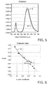
- Fig. 5 shows two emission spectra of red phosphor layers on a blue LED (444nm peak emission) of layers out of the material according to Inventive Example III ("A", solid line) as well as the comparative Example II ("B", dashed line) having identical blue transmission.
- the pcLED using the material according to the invention delivers approx. 6% percent additional light.
- Fig. 6 shows a plot of the total emitted power as a function of the CIE x color coordinate for the two pcLEDs of Fig. 5 ("A" and "B" have the same meaning as in Fig. 5 ).
- the CIE-color coordinate serves as a measure of the ratio of red to blue light in the LED emission spectrum. From the figure it can clearly be seen that the efficiency advantage of the inventive material increases with increasing conversion of light.
- the average diameter can be measured by the following procedure based on light scattering (see XU, R. Particle Characterization: Light Scattering Methods, Kluwer Academic Publishers, Dordrecht (2000 )).
- the powder to be measured is suspended in a liquid media such as demineralized water with a dispersant added to stabilize the suspenion.
- the particle suspension is then analyzed by laser diffraction to obtain information about particle size distribution through measurements of scattering intensity as a function of the scattering angle and the wavelength and polarization of light based on applicable scattering models.
- Such a method is absolute in nature without the need to calibrate instrument.
- particle sizes can be directly measured with a microscope (optical microscope, scanning electron microscope) and particle size distributions can be calculated based on image processing procedures.
Description
- The present invention is directed to novel luminescent materials for light emitting devices, especially to the field of novel luminescent materials for LEDs.
- Phosphors comprising silicates, phosphates (for example, apatite) and aluminates as host materials, with transition metals or rare earth metals added as activating materials to the host materials, are widely known. As blue LEDs, in particular, have become practical in recent years, the development of white light sources utilizing such blue LEDs in combination with such phosphor materials is being energetically pursued.
- Especially red emitting luminescent materials have been in the focus of interest and several materials have been proposed, e.g.
US patent 6680569 (B2), " Red Deficiency Compensating Phosphor for a Light Emitting Device", or fromWO patent application 2005/052087 A1 . -
US2010/289044 describes a white light LED that uses an LED die that emits visible blue light in a wavelength range of about 450-470 nm. A red phosphor or quantum dot material converts some of the blue light to a visible red light having a peak wavelength between about 605-625 nm with a full-width-half-maximum (FWHM) less than 80 nm. A green phosphor or quantum dot material converts some of the blue light to a green light having a FWHM greater than 40 nm, wherein the combination of the blue light, red light, and green light produces a white light providing a color rendering of Ra,8>90 and a color temperature of between 2500K-5000K. Preferably, the red and green converting material do not saturate with an LED die output of 100 W/cm2 and can reliably operate with an LED die junction temperature over 100 degrees C. - However, there is still the continuing need for orange to red emitting luminescent materials which are usable within a wide range of applications and especially allow the fabrication of phosphor warm white pcLEDs with optimized luminous efficiency and color rendering.
- It is an object of the present invention to provide a material which is usable within a wide range of applications and especially allows the fabrication of phosphor warm white pcLEDs with optimized luminous efficiency and color rendering.
- This object is solved by a material according to
claim 1 of the present invention. Accordingly, a material (Ba1-x-y-zSrxCayEu2)2Si5-a-bAlaN8-a-4bOa+4b having an average particle size distribution d50 of ≥ 6 µm is provided, whereby
0.3 ≤ x ≤ 0.9, 0.01 ≤ y ≤ 0.1, 0.005 ≤ z ≤ 0.04,0 ≤ a ≤ 0.2 and 0 ≤ b ≤ 0.2, as further defined in the accompanying claims. - It should be noted that by the term "(Ba1-x-y-zSrxCayEuz)2Si5-a-bAlaN8-a-4bOa+4b" - especially and/or additionally any material is meant and/or included, which has essentially this composition. This goes in analogy for all other materials mentioned in this invention.
- The term "essentially" means especially that ≥ 95 %, preferably ≥ 97 % and most preferred ≥ 99 % wt-%. However, in some applications, trace amounts of additives may also be present in the bulk compositions. These additives particularly include such species known to the art as fluxes. Suitable fluxes include alkaline earth - or alkaline - metal oxides, borates, phosphates and halides such as fluorides, ammonium chloride, SiO2 and the like and mixtures thereof
- Such a material has shown for a wide range of applications within the present invention to have at least one of the following advantages
- Using the material as luminescent material, LEDs may be built which show improved lighting features, especially thermal stability.
- The photostability of the material is greatly enhanced in contrast with materials having a smaller particle size
- The material has a higher emission than comparable materials.
- A similar material is known e.g. from the
US 7,671,529 . However, surprisingly it has been found that by using the material composition as described in this invention, a material with a larger average particle size and - depending on the actual application - furthermore advantageous material features can be achieved. - Without being bound to any theory the inventors believe that it is especially the content of calcium as described which leads to bigger particles (and which will be explained later on in greater detail).
- Therefore this invention also relates to the use of calcium in siliconitridic materials for increasing the average particle size.
- According to a preferred embodiment of the present invention, 0.02 ≤ y ≤ 0.04. It has been shown that a calcium content in this amount is already sufficient to result in greater particle size, on the other hand larger amounts of Ca may possibly lead to unwanted broadening of the emission band and a thus lowered luminous efficiency of the phosphor material.
- According to a preferred embodiment of the present invention, 0.35 ≤ x ≤ 0.8, i.e. the Barium content is somewhat around 20% to 60% mol percent. This has been found to be advantageous for many applications due to the improved luminescence properties of the resulting material.
- According to a preferred embodiment of the present invention, 0 < b ≤ 0.2, i.e. the material comprises oxygen. Surprisingly this has been found to greatly increase the photostability of the material for many applications within the present invention. Without being bound to any theory, it is believed that small amounts of SiN4 tetrahedra containing Si bridging N atoms are removed from the M2Si5N8 lattice and the resulting charge is compensated by terminal O atoms. However, in most applications it has been found that the oxygen content should not be too high, i.e. b should not exceed 0.2.
- According to a preferred embodiment of the present invention, less than 10% of the phosphor particles show an average diameter ≤ 2 µm. This has been found advantageous since by doing so for most applications the photostability may be enhanced.
- According to a preferred embodiment of the present invention, for ≥90% of the phosphor particles the ratio of the longest and shortest particle edge length is ≤ 5. This has been found advantageous since by doing so for most applications the industrial applicability can be easened.
- As described above, the present invention relates to the use of calcium in siliconitridic materials for increasing, the average particle size. This goes especially for materials of the type M2Si5-a-bAlaN8-a-4bOa+4b (with 0 ≤ a ≤ 2 and 0 < b ≤ 2), which are insofar preferred embodiments of the present invention.
- It should be noted that the inventive use of calcium differs from the known use of flux materials, some of which are known to also enhance particle size. According to the invention, calcium is essentially evenly distributed in the powder whereas flux materials are usually not part of the luminescnet material except for impurities.
- According to a preferred embodiment of the present invention, the material has the structure M2Si5-a-bAlaN8-a4bOa+4b, with M being a divalent metal ion and with 0 ≤ a ≤ 2 and 0 ≤ b ≤ 2.
- According to a further preferred embodiment of the present invention, the material has the structure according to the present invention.
- The present invention furthermore relates to a light emitting structure, especially a LED, comprising at least one material according to the present invention.
- The present invention furthermore relates to as system comprising a material according to the present invention and/or materials made according to the inventive methods shown above, being used in one or more of the following applications:
- Office lighting systems
- household application systems
- shop lighting systems,
- home lighting systems,
- accent lighting systems,
- spot lighting systems,
- theater lighting systems,
- fiber-optics application systems,
- projection systems,
- self-lit display systems,
- pixelated display systems,
- segmented display systems,
- warning sign systems,
- medical lighting application systems,
- indicator sign systems, and
- decorative lighting systems
- portable systems
- automotive applications
- green house lighting systems
- The aforementioned components, as well as the claimed components and the components to be used in accordance with the invention in the described embodiments, are not subject to any special exceptions with respect to their size, shape, material selection and technical concept such that the selection criteria known in the pertinent field can be applied without limitations.
- Additional details, features, characteristics and advantages of the object of the invention are disclosed in the subclaims, the figures and the following description of the respective figures and examples, which -- in an exemplary fashion-- show several embodiments and examples an inventive material according to the invention.
- Fig. 1
- shows a scanning electron image of a material according to Example I of the present invention
- Fig. 2
- shows a scanning electron image of a material according to Example II of the present invention
- Fig. 3
- shows a scanning electron image of a material according to a comparative Example
- Fig. 4
- shows a diagramm of emission power vs. layer thickness for for two pcLED comprising an inventive and a comparative material, respectively; and
- Fig. 5
- shows a diagramm of emission vs. wavelength for two pcLEDs comprising the inventive and comparative material of
Fig. 4 , respectively; and - Fig. 6
- shows a plot of the total emitted power as a function of the CIE x color coordinate for the two pcLEDs of
Fig. 5 - The following invention will - together with the figures - futhermore be understood by the following examples which are merely for illustration purposes and which are non- binding.
- All materials - whether inventive or comparative - were made according to the following prescription (and analogous deviations thereof):
- Phosphors of compositions (Ba0.485-0.5xSr0.485-0.5xCaxEu0.03)2Si4.99O0.04N7.96 with varying x = 0, 0.01 and 0.02 have been prepared by mixing of BaH2 (made by hydration of Ba rods, >99% purity), SrH2 (made by hydration of Sr granules, > 99% purity), CaH2 (Aldrich), Eu2Si5N8 (made by reaction of Eu2O3 with carbon and silicon nitride at 1400°C), Si3N4 (UBE SN E-10) with a molar ratio Ba+Sr+Ca+Eu/Si = 0.417 and firing twice with intermediate ball milling at 1620°C in a molybdenum crucible under H2/N2 atmosphere. After ball milling, screening and washing of the powders with 2N HCl, water and isopropanol and final drying, powder phosphors have been obtained.
- A significant effect of Ca addition on grain growth can be observed by the change of particle size distribution (average particle diameter for a given volume fraction, measured by Laser scattering with a Beckman Coulter LS 200 series laser diffraction particle analyzer), as can be seen from Table I:
TABLE I Sample composition Inventive/ Comparative <10vol% <50vol% <90vol% (Ba0.48Sr0.485Eu0.03)2Si4.99O0.04N7.96 Comparative I 2.18 µm 4.03 µm 6.04 µm (Ba0.48Sr0.48Ca0.01Eu0.03)2Si4.99O0.04N7.96 Inventive Example I 2.64 µm 6.15 µm 13.37 µm (Ba0.475Sr0.475Ca0.02Eu0.03)2Si4.99O0.04N7.96 Inventive Example II 5.04 µm 10.27 µm 16.55 µm -
Figs 1 to 3 show scanned electron images of the powders of Inventive Example I, inventive Example II and the comparative Example (no calcium), respectively. - To further illustrate the advantageous feature of the intenive material, the photostability of Inventive Example III (see below) and the Comparative example were investigated.
- It was found that the emission intensity decrease after 1h irradiation with 10 W/cm2 blue light and 260°C phosphor temperature is only 6% for an Inventive Example III while a Comparative Example II (no calcium) shows a decrease of 31 %, as can be seen from Table II:
TABLE II Sample composition Inventive/ Comparative relative emission intensity after 1h, 10 W/cm2 blue flux, T phosphor = 260°C (Ba0.48Sr0.48Ca0.02Eu0.02)2Si4.9O0.04N7.96 Inventive Example III 94% (Ba0.49Sr0.49Eu0.02)2Si4.9Al0.1O0.1N7.9 Comparative II 69% - Further more the optical properties of pcLEDs comprising the material according to Inventive Example III and Comparative Example II were investigated.
Fig. 4 shows the total emitted power of the pcLEDs (red phosphor layers on a blue LED, 444nm peak emission) vs. the layer thickness both for the material of Inventive Example III (diamonds) and Comparative Example II (triangles). For both series, the power decreases with layer thickness, however, the pcLEDs with the material according to the invention always have a higher output power. -
Fig. 5 shows two emission spectra of red phosphor layers on a blue LED (444nm peak emission) of layers out of the material according to Inventive Example III ("A", solid line) as well as the comparative Example II ("B", dashed line) having identical blue transmission. The pcLED using the material according to the invention delivers approx. 6% percent additional light. -
Fig. 6 shows a plot of the total emitted power as a function of the CIE x color coordinate for the two pcLEDs ofFig. 5 ("A" and "B" have the same meaning as inFig. 5 ). The CIE-color coordinate serves as a measure of the ratio of red to blue light in the LED emission spectrum. From the figure it can clearly be seen that the efficiency advantage of the inventive material increases with increasing conversion of light. - The particular combinations of elements and features in the above detailed embodiments are exemplary only; the interchanging and substitution of these teachings with other teachings in this and the patents/applications incorporated by reference are also expressly contemplated. As those skilled in the art will recognize, variations, modifications, and other implementations of what is described herein can occur to those of ordinary skill in the art without departing from the spirit and the scope of the invention as claimed. Accordingly, the foregoing description is by way of example only and is not intended as limiting. In the claims, the word "comprising" does not exclude other elements or steps, and the indefinite article "a" or "an" does not exclude a plurality. The mere fact that certain measures are recited in mutually different dependent claims does not indicate that a combination of these measured cannot be used to advantage. The invention's scope is defined in the following claims and the equivalents thereto. Furthermore, reference signs used in the description and claims do not limit the scope of the invention as claimed.
- The average diameter can be measured by the following procedure based on light scattering (see XU, R. Particle Characterization: Light Scattering Methods, Kluwer Academic Publishers, Dordrecht (2000)). The powder to be measured is suspended in a liquid media such as demineralized water with a dispersant added to stabilize the suspenion. The particle suspension is then analyzed by laser diffraction to obtain information about particle size distribution through measurements of scattering intensity as a function of the scattering angle and the wavelength and polarization of light based on applicable scattering models. Such a method is absolute in nature without the need to calibrate instrument. Alternatively, particle sizes can be directly measured with a microscope (optical microscope, scanning electron microscope) and particle size distributions can be calculated based on image processing procedures.
Claims (6)
- (Ba1-x-y-zSrxCayEuz)2Si5-a-bAlaN8-a-4bOa+4b having an average particle size distribution d50 of ≥ 6 µm, whereby

- The material of claim 1, whereby 0.02 ≤ y ≤ 0.04.
- The material of claim 1 or 2, whereby 0.35 ≤ x ≤ 0.8.
- The material of any of the claims 1 to 3, whereby 0 < b ≤ 0.2, and wherein a=0.
- A light emitting structure, especially a LED, comprising a material according to any of the claims 1 to 4.
- A system comprising a material according to any of the claims 1 to 4 and/or comprising a light emitting structure according to Claim 5, the system being used in one or more of the following applications:- Office lighting systems- household application systems- shop lighting systems,- home lighting systems,- accent lighting systems,- spot lighting systems,- theater lighting systems,- fiber-optics application systems,- projection systems,- self-lit display systems,- pixelated display systems,- segmented display systems,- warning sign systems,- medical lighting application systems,- indicator sign systems,- decorative lighting systems,- portable systems,- automotive applications,- green house lighting systems.
Priority Applications (1)
| Application Number | Priority Date | Filing Date | Title |
|---|---|---|---|
| EP11797150.7A EP2646523B1 (en) | 2010-12-01 | 2011-11-28 | Red emitting luminescent materials |
Applications Claiming Priority (3)
| Application Number | Priority Date | Filing Date | Title |
|---|---|---|---|
| EP10193251 | 2010-12-01 | ||
| EP11797150.7A EP2646523B1 (en) | 2010-12-01 | 2011-11-28 | Red emitting luminescent materials |
| PCT/IB2011/055329 WO2012073177A1 (en) | 2010-12-01 | 2011-11-28 | Red emitting luminescent materials |
Publications (2)
| Publication Number | Publication Date |
|---|---|
| EP2646523A1 EP2646523A1 (en) | 2013-10-09 |
| EP2646523B1 true EP2646523B1 (en) | 2015-11-25 |
Family
ID=45350440
Family Applications (1)
| Application Number | Title | Priority Date | Filing Date |
|---|---|---|---|
| EP11797150.7A Active EP2646523B1 (en) | 2010-12-01 | 2011-11-28 | Red emitting luminescent materials |
Country Status (9)
| Country | Link |
|---|---|
| US (1) | US9257607B2 (en) |
| EP (1) | EP2646523B1 (en) |
| JP (1) | JP5970467B2 (en) |
| KR (1) | KR101810234B1 (en) |
| CN (2) | CN103314072A (en) |
| BR (1) | BR112013013485B1 (en) |
| RU (1) | RU2591943C2 (en) |
| TW (1) | TWI537364B (en) |
| WO (1) | WO2012073177A1 (en) |
Families Citing this family (22)
| Publication number | Priority date | Publication date | Assignee | Title |
|---|---|---|---|---|
| TWI494413B (en) | 2012-12-22 | 2015-08-01 | Chi Mei Corp | Phosphor and light emitting device |
| TWI464238B (en) * | 2013-03-27 | 2014-12-11 | Chi Mei Corp | Phosphor and light emitting device |
| KR102396732B1 (en) | 2014-10-31 | 2022-05-12 | 루미리즈 홀딩 비.브이. | Phosphor converted led with temperature stable flux and saturated red color point |
| CN104371712A (en) * | 2014-11-03 | 2015-02-25 | 天津理工大学 | Normal-pressure preparation method of calcium-base nitride red fluorescent powder |
| CN107109216A (en) * | 2014-12-24 | 2017-08-29 | 皇家飞利浦有限公司 | The LED of phosphor converted |
| JP6735487B2 (en) * | 2016-03-28 | 2020-08-05 | 国立研究開発法人物質・材料研究機構 | Phosphor, manufacturing method thereof, light emitting device, image display device, pigment and ultraviolet absorber |
| WO2017170453A1 (en) * | 2016-03-28 | 2017-10-05 | 国立研究開発法人物質・材料研究機構 | Phosphor, method for producing same, light emitting device, image display, pigment and ultraviolet light absorber |
| JP6700633B2 (en) * | 2016-03-28 | 2020-05-27 | 国立研究開発法人物質・材料研究機構 | Phosphor, manufacturing method thereof, light emitting device, image display device, pigment and ultraviolet absorber |
| JP6700631B2 (en) * | 2016-03-28 | 2020-05-27 | 国立研究開発法人物質・材料研究機構 | Phosphor, manufacturing method thereof, light emitting device, image display device, pigment and ultraviolet absorber |
| JP6700632B2 (en) * | 2016-03-28 | 2020-05-27 | 国立研究開発法人物質・材料研究機構 | Phosphor, manufacturing method thereof, light emitting device, image display device, pigment and ultraviolet absorber |
| JP6700630B2 (en) * | 2016-03-28 | 2020-05-27 | 国立研究開発法人物質・材料研究機構 | Phosphor, manufacturing method thereof, light emitting device, image display device, pigment and ultraviolet absorber |
| DE102016121692A1 (en) | 2016-08-12 | 2018-02-15 | Osram Gmbh | Phosphor and method of making a phosphor |
| WO2018029304A1 (en) | 2016-08-12 | 2018-02-15 | Osram Gmbh | Illumination device |
| US10644206B2 (en) | 2016-08-12 | 2020-05-05 | Osram Oled Gmbh | Lighting device |
| US10711192B2 (en) | 2016-08-12 | 2020-07-14 | Osram Oled Gmbh | Lighting device |
| JP7050774B2 (en) | 2016-11-11 | 2022-04-08 | オスラム オプト セミコンダクターズ ゲゼルシャフト ミット ベシュレンクテル ハフツング | Use of phosphors, luminaires and luminaires |
| US10519371B2 (en) | 2016-11-11 | 2019-12-31 | Osram Opto Semiconductors Gmbh | Phosphor, illumination device and use of an illumination device |
| WO2019029849A1 (en) | 2016-11-11 | 2019-02-14 | Osram Opto Semiconductors Gmbh | Dimmable light source |
| US10837607B2 (en) | 2017-09-26 | 2020-11-17 | Lumileds Llc | Light emitting device with improved warm-white color point |
| DE102018205464A1 (en) | 2017-11-10 | 2019-05-16 | Osram Opto Semiconductors Gmbh | LIGHTING DEVICE AND USE OF A LIGHTING DEVICE |
| RU2693781C2 (en) * | 2017-12-12 | 2019-07-04 | Федеральное государственное бюджетное учреждение науки Ордена Трудового Красного Знамени Институт химии силикатов им. И.В. Гребенщикова Российской академии наук (ИХС РАН) | Red-emitting photoluminescent phosphor material for plasma panels screens |
| JP2022038930A (en) * | 2020-08-27 | 2022-03-10 | 住友化学株式会社 | Luminescent compound particle, and luminescent compound particle composition |
Citations (1)
| Publication number | Priority date | Publication date | Assignee | Title |
|---|---|---|---|---|
| US20100289044A1 (en) * | 2009-05-12 | 2010-11-18 | Koninklijke Philips Electronics N.V. | Wavelength conversion for producing white light from high power blue led |
Family Cites Families (35)
| Publication number | Priority date | Publication date | Assignee | Title |
|---|---|---|---|---|
| SU1039951A1 (en) * | 1981-12-18 | 1983-09-07 | Ленинградский Ордена Ленина Политехнический Институт Им.М.И.Калинина | Luminiscent composition |
| US6680569B2 (en) * | 1999-02-18 | 2004-01-20 | Lumileds Lighting U.S. Llc | Red-deficiency compensating phosphor light emitting device |
| EP1104799A1 (en) | 1999-11-30 | 2001-06-06 | Patent-Treuhand-Gesellschaft für elektrische Glühlampen mbH | Red emitting luminescent material |
| DE10147040A1 (en) * | 2001-09-25 | 2003-04-24 | Patent Treuhand Ges Fuer Elektrische Gluehlampen Mbh | Lighting unit with at least one LED as a light source |
| JP4193471B2 (en) * | 2001-12-14 | 2008-12-10 | 日亜化学工業株式会社 | Light emitting device and manufacturing method thereof |
| US6924514B2 (en) * | 2002-02-19 | 2005-08-02 | Nichia Corporation | Light-emitting device and process for producing thereof |
| US6717353B1 (en) * | 2002-10-14 | 2004-04-06 | Lumileds Lighting U.S., Llc | Phosphor converted light emitting device |
| JP4207537B2 (en) * | 2002-11-08 | 2009-01-14 | 日亜化学工業株式会社 | Phosphor and light emitting device |
| US7723740B2 (en) * | 2003-09-18 | 2010-05-25 | Nichia Corporation | Light emitting device |
| JP2005093912A (en) * | 2003-09-19 | 2005-04-07 | Nichia Chem Ind Ltd | Light-emitting device |
| JP3837588B2 (en) | 2003-11-26 | 2006-10-25 | 独立行政法人物質・材料研究機構 | Phosphors and light emitting devices using phosphors |
| TW200604325A (en) * | 2004-03-22 | 2006-02-01 | Fujikura Ltd | Light-emitting device and illuminating device |
| JP4581120B2 (en) | 2004-04-26 | 2010-11-17 | 独立行政法人物質・材料研究機構 | Oxynitride powder and method for producing the same |
| WO2005103199A1 (en) * | 2004-04-27 | 2005-11-03 | Matsushita Electric Industrial Co., Ltd. | Phosphor composition and method for producing the same, and light-emitting device using the same |
| US6956247B1 (en) * | 2004-05-26 | 2005-10-18 | Lumileds Lighting U.S., Llc | Semiconductor light emitting device including photonic band gap material and luminescent material |
| EP1780255B1 (en) * | 2004-07-13 | 2012-04-18 | Fujikura, Ltd. | Fluorescent substance and light bulb color light emitting diode lamp using the fluorescent substance and emitting light bulb color light |
| US8417215B2 (en) * | 2004-07-28 | 2013-04-09 | Koninklijke Philips Electronics N.V. | Method for positioning of wireless medical devices with short-range radio frequency technology |
| JP4674348B2 (en) | 2004-09-22 | 2011-04-20 | 独立行政法人物質・材料研究機構 | Phosphor, method for producing the same, and light emitting device |
| US7540977B2 (en) * | 2004-09-22 | 2009-06-02 | National Institute For Materials Science | Phosphor, production method thereof and light emitting instrument |
| RU2315078C2 (en) * | 2004-10-18 | 2008-01-20 | Общество с ограниченной ответственностью Научно-производственная компания "Люминифор-Платан" (ООО НПК "Люминофор-Платан") | Photoluminophores for short-wave light-emitting diodes (led) |
| US7671529B2 (en) * | 2004-12-10 | 2010-03-02 | Philips Lumileds Lighting Company, Llc | Phosphor converted light emitting device |
| JP2006213910A (en) * | 2005-01-06 | 2006-08-17 | Matsushita Electric Ind Co Ltd | Oxynitride phosphor and light-emitting device |
| CN101138278A (en) * | 2005-03-09 | 2008-03-05 | 皇家飞利浦电子股份有限公司 | Illumination system comprising a radiation source and a fluorescent material |
| KR20080009198A (en) * | 2005-03-31 | 2008-01-25 | 도와 일렉트로닉스 가부시키가이샤 | Phosphor phosphor sheet, and manufacturing method therefore, and light emission device using the phosphor |
| JP4761848B2 (en) * | 2005-06-22 | 2011-08-31 | 株式会社東芝 | Semiconductor light emitting device |
| TWI266563B (en) * | 2005-08-12 | 2006-11-11 | Epistar Corp | Compound, phosphor composition and light-emitting device containing the same |
| KR101459999B1 (en) | 2006-04-25 | 2014-11-10 | 코닌클리케 필립스 엔.브이. | Fluorescent lighting creating white light |
| KR101221691B1 (en) * | 2006-05-10 | 2013-01-11 | 덴끼 가가꾸 고교 가부시키가이샤 | Sialon phosphor, process for producing the same, and illuminator and luminescent element employing the same |
| DE602008006033D1 (en) | 2007-02-06 | 2011-05-19 | Philips Intellectual Property | RED LIGHT EMITTING LUMINESCENT OXYNITRIDE MATERIALS |
| CN101157854B (en) | 2007-07-02 | 2010-10-13 | 北京宇极科技发展有限公司 | Oxynitrides luminescent material, preparation method and uses thereof |
| WO2009008250A1 (en) * | 2007-07-09 | 2009-01-15 | Sharp Kabushiki Kaisha | Group of phosphor particles, and light-emitting device using the same |
| JP2009096882A (en) * | 2007-10-17 | 2009-05-07 | Denki Kagaku Kogyo Kk | Phosphor and method for producing the same |
| JP2009221318A (en) * | 2008-03-14 | 2009-10-01 | Tokyo Institute Of Technology | Method for producing phosphor, phosphor-containing composition, light emitting device, image display device and illuminating device |
| US8691113B2 (en) * | 2008-07-02 | 2014-04-08 | Dexerials Corporation | Red phosphor, method for producing red phosphor, white light source, illuminating device, and liquid crystal display device |
| EP2383324A4 (en) * | 2009-01-27 | 2012-08-15 | Denki Kagaku Kogyo Kk | -sialon phosphor, method for producing same, and light-emitting device |
-
2011
- 2011-11-28 CN CN201180058117XA patent/CN103314072A/en active Pending
- 2011-11-28 KR KR1020137016983A patent/KR101810234B1/en active IP Right Grant
- 2011-11-28 EP EP11797150.7A patent/EP2646523B1/en active Active
- 2011-11-28 RU RU2013129842/05A patent/RU2591943C2/en active
- 2011-11-28 CN CN201710233851.4A patent/CN107011904A/en active Pending
- 2011-11-28 BR BR112013013485-2A patent/BR112013013485B1/en active IP Right Grant
- 2011-11-28 US US13/988,852 patent/US9257607B2/en active Active
- 2011-11-28 JP JP2013541455A patent/JP5970467B2/en active Active
- 2011-11-28 WO PCT/IB2011/055329 patent/WO2012073177A1/en active Application Filing
- 2011-11-30 TW TW100144029A patent/TWI537364B/en active
Patent Citations (1)
| Publication number | Priority date | Publication date | Assignee | Title |
|---|---|---|---|---|
| US20100289044A1 (en) * | 2009-05-12 | 2010-11-18 | Koninklijke Philips Electronics N.V. | Wavelength conversion for producing white light from high power blue led |
Also Published As
| Publication number | Publication date |
|---|---|
| EP2646523A1 (en) | 2013-10-09 |
| CN107011904A (en) | 2017-08-04 |
| BR112013013485A2 (en) | 2016-10-11 |
| TWI537364B (en) | 2016-06-11 |
| TW201229212A (en) | 2012-07-16 |
| US9257607B2 (en) | 2016-02-09 |
| WO2012073177A1 (en) | 2012-06-07 |
| CN103314072A (en) | 2013-09-18 |
| JP5970467B2 (en) | 2016-08-17 |
| KR20130131392A (en) | 2013-12-03 |
| US20130240943A1 (en) | 2013-09-19 |
| KR101810234B1 (en) | 2017-12-18 |
| BR112013013485B1 (en) | 2020-12-29 |
| RU2591943C2 (en) | 2016-07-20 |
| JP2014504312A (en) | 2014-02-20 |
| RU2013129842A (en) | 2015-01-10 |
Similar Documents
| Publication | Publication Date | Title |
|---|---|---|
| EP2646523B1 (en) | Red emitting luminescent materials | |
| TWI399422B (en) | Fluorescence material and manufacture thereof and luminaire | |
| JP7025673B2 (en) | Nitride phosphor manufacturing method and nitride phosphor | |
| JP4933739B2 (en) | Phosphor and phosphor film for electron beam excitation, and color display device using them | |
| TWI476268B (en) | Phosphor, manufacture thereof, light-emitting device, and image display device | |
| JP6852780B2 (en) | Manufacturing method of wavelength conversion member | |
| TWI582214B (en) | Phosphor, manufacture thereof, light-emitting device, image display device, pigment, and ultraviolet absorber utilizing phosphor | |
| WO2016186057A1 (en) | Phosphor, production method for same, illumination instrument, and image display device | |
| JP6658690B2 (en) | Nitride phosphor, manufacturing method thereof and light emitting device | |
| KR20070021140A (en) | Phosphor, process for producing the same, lighting fixture and image display unit | |
| KR101876103B1 (en) | Oxynitride fluorescent substance powder, silicon nitride powder for manufacturing same, and method for manufacturing same | |
| JP2010241995A (en) | beta-TYPE SIALON PHOSPHOR, METHOD FOR PRODUCING THE SAME AND APPLICATION OF THE SAME | |
| WO2016186058A1 (en) | Light-emitting instrument and image display device | |
| JP3975451B2 (en) | Luminaire and image display device using phosphor | |
| JP2016216711A (en) | Phosphor, production method of the same, lighting apparatus and image display device | |
| JP6414190B2 (en) | Method for manufacturing phosphor | |
| JP5874198B2 (en) | Phosphor, method for producing phosphor, and light emitting device using the phosphor | |
| JP6940778B2 (en) | Nitride phosphor manufacturing method | |
| JP5866870B2 (en) | Light emitting device | |
| JP2010043280A (en) | Fluorescent substance, shift method of the emission wavelength, light source, and led | |
| JP2018150433A (en) | Orange phosphor and light-emitting device |
Legal Events
| Date | Code | Title | Description |
|---|---|---|---|
| PUAI | Public reference made under article 153(3) epc to a published international application that has entered the european phase |
Free format text: ORIGINAL CODE: 0009012 |
|
| 17P | Request for examination filed |
Effective date: 20130701 |
|
| AK | Designated contracting states |
Kind code of ref document: A1 Designated state(s): AL AT BE BG CH CY CZ DE DK EE ES FI FR GB GR HR HU IE IS IT LI LT LU LV MC MK MT NL NO PL PT RO RS SE SI SK SM TR |
|
| DAX | Request for extension of the european patent (deleted) | ||
| 17Q | First examination report despatched |
Effective date: 20140903 |
|
| REG | Reference to a national code |
Ref country code: DE Ref legal event code: R079 Ref document number: 602011021687 Country of ref document: DE Free format text: PREVIOUS MAIN CLASS: C09K0011080000 Ipc: C09K0011590000 |
|
| GRAP | Despatch of communication of intention to grant a patent |
Free format text: ORIGINAL CODE: EPIDOSNIGR1 |
|
| INTG | Intention to grant announced |
Effective date: 20150626 |
|
| RIC1 | Information provided on ipc code assigned before grant |
Ipc: H01L 33/50 20100101ALN20150617BHEP Ipc: C09K 11/59 20060101AFI20150617BHEP |
|
| GRAS | Grant fee paid |
Free format text: ORIGINAL CODE: EPIDOSNIGR3 |
|
| GRAA | (expected) grant |
Free format text: ORIGINAL CODE: 0009210 |
|
| AK | Designated contracting states |
Kind code of ref document: B1 Designated state(s): AL AT BE BG CH CY CZ DE DK EE ES FI FR GB GR HR HU IE IS IT LI LT LU LV MC MK MT NL NO PL PT RO RS SE SI SK SM TR |
|
| REG | Reference to a national code |
Ref country code: GB Ref legal event code: FG4D |
|
| REG | Reference to a national code |
Ref country code: CH Ref legal event code: EP Ref country code: FR Ref legal event code: PLFP Year of fee payment: 5 |
|
| REG | Reference to a national code |
Ref country code: AT Ref legal event code: REF Ref document number: 762597 Country of ref document: AT Kind code of ref document: T Effective date: 20151215 |
|
| REG | Reference to a national code |
Ref country code: IE Ref legal event code: FG4D |
|
| REG | Reference to a national code |
Ref country code: DE Ref legal event code: R096 Ref document number: 602011021687 Country of ref document: DE |
|
| REG | Reference to a national code |
Ref country code: LT Ref legal event code: MG4D |
|
| REG | Reference to a national code |
Ref country code: NL Ref legal event code: MP Effective date: 20160225 |
|
| REG | Reference to a national code |
Ref country code: AT Ref legal event code: MK05 Ref document number: 762597 Country of ref document: AT Kind code of ref document: T Effective date: 20151125 |
|
| PG25 | Lapsed in a contracting state [announced via postgrant information from national office to epo] |
Ref country code: IS Free format text: LAPSE BECAUSE OF FAILURE TO SUBMIT A TRANSLATION OF THE DESCRIPTION OR TO PAY THE FEE WITHIN THE PRESCRIBED TIME-LIMIT Effective date: 20160325 Ref country code: HR Free format text: LAPSE BECAUSE OF FAILURE TO SUBMIT A TRANSLATION OF THE DESCRIPTION OR TO PAY THE FEE WITHIN THE PRESCRIBED TIME-LIMIT Effective date: 20151125 Ref country code: NO Free format text: LAPSE BECAUSE OF FAILURE TO SUBMIT A TRANSLATION OF THE DESCRIPTION OR TO PAY THE FEE WITHIN THE PRESCRIBED TIME-LIMIT Effective date: 20160225 Ref country code: NL Free format text: LAPSE BECAUSE OF FAILURE TO SUBMIT A TRANSLATION OF THE DESCRIPTION OR TO PAY THE FEE WITHIN THE PRESCRIBED TIME-LIMIT Effective date: 20151125 Ref country code: ES Free format text: LAPSE BECAUSE OF FAILURE TO SUBMIT A TRANSLATION OF THE DESCRIPTION OR TO PAY THE FEE WITHIN THE PRESCRIBED TIME-LIMIT Effective date: 20151125 Ref country code: LT Free format text: LAPSE BECAUSE OF FAILURE TO SUBMIT A TRANSLATION OF THE DESCRIPTION OR TO PAY THE FEE WITHIN THE PRESCRIBED TIME-LIMIT Effective date: 20151125 |
|
| PG25 | Lapsed in a contracting state [announced via postgrant information from national office to epo] |
Ref country code: LV Free format text: LAPSE BECAUSE OF FAILURE TO SUBMIT A TRANSLATION OF THE DESCRIPTION OR TO PAY THE FEE WITHIN THE PRESCRIBED TIME-LIMIT Effective date: 20151125 Ref country code: BE Free format text: LAPSE BECAUSE OF NON-PAYMENT OF DUE FEES Effective date: 20151130 Ref country code: AT Free format text: LAPSE BECAUSE OF FAILURE TO SUBMIT A TRANSLATION OF THE DESCRIPTION OR TO PAY THE FEE WITHIN THE PRESCRIBED TIME-LIMIT Effective date: 20151125 Ref country code: SE Free format text: LAPSE BECAUSE OF FAILURE TO SUBMIT A TRANSLATION OF THE DESCRIPTION OR TO PAY THE FEE WITHIN THE PRESCRIBED TIME-LIMIT Effective date: 20151125 Ref country code: PT Free format text: LAPSE BECAUSE OF FAILURE TO SUBMIT A TRANSLATION OF THE DESCRIPTION OR TO PAY THE FEE WITHIN THE PRESCRIBED TIME-LIMIT Effective date: 20160325 Ref country code: FI Free format text: LAPSE BECAUSE OF FAILURE TO SUBMIT A TRANSLATION OF THE DESCRIPTION OR TO PAY THE FEE WITHIN THE PRESCRIBED TIME-LIMIT Effective date: 20151125 Ref country code: PL Free format text: LAPSE BECAUSE OF FAILURE TO SUBMIT A TRANSLATION OF THE DESCRIPTION OR TO PAY THE FEE WITHIN THE PRESCRIBED TIME-LIMIT Effective date: 20151125 Ref country code: RS Free format text: LAPSE BECAUSE OF FAILURE TO SUBMIT A TRANSLATION OF THE DESCRIPTION OR TO PAY THE FEE WITHIN THE PRESCRIBED TIME-LIMIT Effective date: 20151125 Ref country code: GR Free format text: LAPSE BECAUSE OF FAILURE TO SUBMIT A TRANSLATION OF THE DESCRIPTION OR TO PAY THE FEE WITHIN THE PRESCRIBED TIME-LIMIT Effective date: 20160226 |
|
| REG | Reference to a national code |
Ref country code: CH Ref legal event code: PL |
|
| PG25 | Lapsed in a contracting state [announced via postgrant information from national office to epo] |
Ref country code: CZ Free format text: LAPSE BECAUSE OF FAILURE TO SUBMIT A TRANSLATION OF THE DESCRIPTION OR TO PAY THE FEE WITHIN THE PRESCRIBED TIME-LIMIT Effective date: 20151125 Ref country code: LI Free format text: LAPSE BECAUSE OF NON-PAYMENT OF DUE FEES Effective date: 20151130 Ref country code: CH Free format text: LAPSE BECAUSE OF NON-PAYMENT OF DUE FEES Effective date: 20151130 Ref country code: IT Free format text: LAPSE BECAUSE OF FAILURE TO SUBMIT A TRANSLATION OF THE DESCRIPTION OR TO PAY THE FEE WITHIN THE PRESCRIBED TIME-LIMIT Effective date: 20151125 |
|
| REG | Reference to a national code |
Ref country code: IE Ref legal event code: MM4A |
|
| REG | Reference to a national code |
Ref country code: DE Ref legal event code: R097 Ref document number: 602011021687 Country of ref document: DE |
|
| PG25 | Lapsed in a contracting state [announced via postgrant information from national office to epo] |
Ref country code: RO Free format text: LAPSE BECAUSE OF FAILURE TO SUBMIT A TRANSLATION OF THE DESCRIPTION OR TO PAY THE FEE WITHIN THE PRESCRIBED TIME-LIMIT Effective date: 20151125 Ref country code: SM Free format text: LAPSE BECAUSE OF FAILURE TO SUBMIT A TRANSLATION OF THE DESCRIPTION OR TO PAY THE FEE WITHIN THE PRESCRIBED TIME-LIMIT Effective date: 20151125 Ref country code: DK Free format text: LAPSE BECAUSE OF FAILURE TO SUBMIT A TRANSLATION OF THE DESCRIPTION OR TO PAY THE FEE WITHIN THE PRESCRIBED TIME-LIMIT Effective date: 20151125 Ref country code: SK Free format text: LAPSE BECAUSE OF FAILURE TO SUBMIT A TRANSLATION OF THE DESCRIPTION OR TO PAY THE FEE WITHIN THE PRESCRIBED TIME-LIMIT Effective date: 20151125 Ref country code: EE Free format text: LAPSE BECAUSE OF FAILURE TO SUBMIT A TRANSLATION OF THE DESCRIPTION OR TO PAY THE FEE WITHIN THE PRESCRIBED TIME-LIMIT Effective date: 20151125 |
|
| PG25 | Lapsed in a contracting state [announced via postgrant information from national office to epo] |
Ref country code: MC Free format text: LAPSE BECAUSE OF FAILURE TO SUBMIT A TRANSLATION OF THE DESCRIPTION OR TO PAY THE FEE WITHIN THE PRESCRIBED TIME-LIMIT Effective date: 20151125 |
|
| PLBE | No opposition filed within time limit |
Free format text: ORIGINAL CODE: 0009261 |
|
| STAA | Information on the status of an ep patent application or granted ep patent |
Free format text: STATUS: NO OPPOSITION FILED WITHIN TIME LIMIT |
|
| PG25 | Lapsed in a contracting state [announced via postgrant information from national office to epo] |
Ref country code: IE Free format text: LAPSE BECAUSE OF NON-PAYMENT OF DUE FEES Effective date: 20151128 |
|
| 26N | No opposition filed |
Effective date: 20160826 |
|
| REG | Reference to a national code |
Ref country code: FR Ref legal event code: PLFP Year of fee payment: 6 |
|
| PG25 | Lapsed in a contracting state [announced via postgrant information from national office to epo] |
Ref country code: SI Free format text: LAPSE BECAUSE OF FAILURE TO SUBMIT A TRANSLATION OF THE DESCRIPTION OR TO PAY THE FEE WITHIN THE PRESCRIBED TIME-LIMIT Effective date: 20151125 |
|
| PG25 | Lapsed in a contracting state [announced via postgrant information from national office to epo] |
Ref country code: BE Free format text: LAPSE BECAUSE OF FAILURE TO SUBMIT A TRANSLATION OF THE DESCRIPTION OR TO PAY THE FEE WITHIN THE PRESCRIBED TIME-LIMIT Effective date: 20151125 |
|
| PG25 | Lapsed in a contracting state [announced via postgrant information from national office to epo] |
Ref country code: BG Free format text: LAPSE BECAUSE OF FAILURE TO SUBMIT A TRANSLATION OF THE DESCRIPTION OR TO PAY THE FEE WITHIN THE PRESCRIBED TIME-LIMIT Effective date: 20151125 Ref country code: HU Free format text: LAPSE BECAUSE OF FAILURE TO SUBMIT A TRANSLATION OF THE DESCRIPTION OR TO PAY THE FEE WITHIN THE PRESCRIBED TIME-LIMIT; INVALID AB INITIO Effective date: 20111128 |
|
| PG25 | Lapsed in a contracting state [announced via postgrant information from national office to epo] |
Ref country code: CY Free format text: LAPSE BECAUSE OF FAILURE TO SUBMIT A TRANSLATION OF THE DESCRIPTION OR TO PAY THE FEE WITHIN THE PRESCRIBED TIME-LIMIT Effective date: 20151125 |
|
| PG25 | Lapsed in a contracting state [announced via postgrant information from national office to epo] |
Ref country code: MT Free format text: LAPSE BECAUSE OF FAILURE TO SUBMIT A TRANSLATION OF THE DESCRIPTION OR TO PAY THE FEE WITHIN THE PRESCRIBED TIME-LIMIT Effective date: 20151125 |
|
| REG | Reference to a national code |
Ref country code: FR Ref legal event code: PLFP Year of fee payment: 7 |
|
| PG25 | Lapsed in a contracting state [announced via postgrant information from national office to epo] |
Ref country code: LU Free format text: LAPSE BECAUSE OF NON-PAYMENT OF DUE FEES Effective date: 20151128 |
|
| REG | Reference to a national code |
Ref country code: FR Ref legal event code: CA Effective date: 20180126 Ref country code: FR Ref legal event code: TP Owner name: LUMILEDS HOLDING B.V., NL Effective date: 20180126 |
|
| PG25 | Lapsed in a contracting state [announced via postgrant information from national office to epo] |
Ref country code: MK Free format text: LAPSE BECAUSE OF FAILURE TO SUBMIT A TRANSLATION OF THE DESCRIPTION OR TO PAY THE FEE WITHIN THE PRESCRIBED TIME-LIMIT Effective date: 20151125 Ref country code: TR Free format text: LAPSE BECAUSE OF FAILURE TO SUBMIT A TRANSLATION OF THE DESCRIPTION OR TO PAY THE FEE WITHIN THE PRESCRIBED TIME-LIMIT Effective date: 20151125 |
|
| REG | Reference to a national code |
Ref country code: GB Ref legal event code: 732E Free format text: REGISTERED BETWEEN 20180920 AND 20180926 |
|
| PG25 | Lapsed in a contracting state [announced via postgrant information from national office to epo] |
Ref country code: AL Free format text: LAPSE BECAUSE OF FAILURE TO SUBMIT A TRANSLATION OF THE DESCRIPTION OR TO PAY THE FEE WITHIN THE PRESCRIBED TIME-LIMIT Effective date: 20151125 |
|
| REG | Reference to a national code |
Ref country code: DE Ref legal event code: R081 Ref document number: 602011021687 Country of ref document: DE Owner name: LUMILEDS HOLDING B.V., NL Free format text: FORMER OWNER: PHILIPS INTELLECTUAL PROPERTY & STANDARDS GMBH, 20099 HAMBURG, DE |
|
| P01 | Opt-out of the competence of the unified patent court (upc) registered |
Effective date: 20230530 |
|
| PGFP | Annual fee paid to national office [announced via postgrant information from national office to epo] |
Ref country code: GB Payment date: 20231121 Year of fee payment: 13 |
|
| PGFP | Annual fee paid to national office [announced via postgrant information from national office to epo] |
Ref country code: FR Payment date: 20231123 Year of fee payment: 13 Ref country code: DE Payment date: 20231127 Year of fee payment: 13 |