EP2645581A2 - Wireless communication device - Google Patents
Wireless communication device Download PDFInfo
- Publication number
- EP2645581A2 EP2645581A2 EP12197667.4A EP12197667A EP2645581A2 EP 2645581 A2 EP2645581 A2 EP 2645581A2 EP 12197667 A EP12197667 A EP 12197667A EP 2645581 A2 EP2645581 A2 EP 2645581A2
- Authority
- EP
- European Patent Office
- Prior art keywords
- signal
- correction value
- mixer
- wireless communication
- communication device
- Prior art date
- Legal status (The legal status is an assumption and is not a legal conclusion. Google has not performed a legal analysis and makes no representation as to the accuracy of the status listed.)
- Granted
Links
Images


Classifications
-
- H—ELECTRICITY
- H04—ELECTRIC COMMUNICATION TECHNIQUE
- H04L—TRANSMISSION OF DIGITAL INFORMATION, e.g. TELEGRAPHIC COMMUNICATION
- H04L5/00—Arrangements affording multiple use of the transmission path
- H04L5/14—Two-way operation using the same type of signal, i.e. duplex
-
- H—ELECTRICITY
- H04—ELECTRIC COMMUNICATION TECHNIQUE
- H04B—TRANSMISSION
- H04B1/00—Details of transmission systems, not covered by a single one of groups H04B3/00 - H04B13/00; Details of transmission systems not characterised by the medium used for transmission
- H04B1/02—Transmitters
- H04B1/04—Circuits
-
- H—ELECTRICITY
- H04—ELECTRIC COMMUNICATION TECHNIQUE
- H04B—TRANSMISSION
- H04B1/00—Details of transmission systems, not covered by a single one of groups H04B3/00 - H04B13/00; Details of transmission systems not characterised by the medium used for transmission
- H04B1/02—Transmitters
- H04B1/04—Circuits
- H04B1/0475—Circuits with means for limiting noise, interference or distortion
-
- H—ELECTRICITY
- H04—ELECTRIC COMMUNICATION TECHNIQUE
- H04B—TRANSMISSION
- H04B17/00—Monitoring; Testing
- H04B17/10—Monitoring; Testing of transmitters
- H04B17/11—Monitoring; Testing of transmitters for calibration
- H04B17/14—Monitoring; Testing of transmitters for calibration of the whole transmission and reception path, e.g. self-test loop-back
-
- H—ELECTRICITY
- H04—ELECTRIC COMMUNICATION TECHNIQUE
- H04L—TRANSMISSION OF DIGITAL INFORMATION, e.g. TELEGRAPHIC COMMUNICATION
- H04L27/00—Modulated-carrier systems
- H04L27/32—Carrier systems characterised by combinations of two or more of the types covered by groups H04L27/02, H04L27/10, H04L27/18 or H04L27/26
- H04L27/34—Amplitude- and phase-modulated carrier systems, e.g. quadrature-amplitude modulated carrier systems
- H04L27/36—Modulator circuits; Transmitter circuits
- H04L27/362—Modulation using more than one carrier, e.g. with quadrature carriers, separately amplitude modulated
- H04L27/364—Arrangements for overcoming imperfections in the modulator, e.g. quadrature error or unbalanced I and Q levels
Definitions
- the embodiments discussed herein are directed to a wireless communication device.
- FIG. 1 illustrates an example of frequency characteristics of a duplexer that is used in a wireless communication device mounted on a communication terminal device (hereinafter, abbreviated as "communication terminal") such as a mobile phone.
- communication terminal such as a mobile phone.
- ripple deviations occur in the transmission bandwidth of 1920 to 1980 MHz.
- the ripple deviations vary depending on each individual duplexer due to the temperature change, the variation in the elements, the difference of manufacturers, the difference of models even in the same manufacture, or the like. It is difficult to further improve the performance of the duplexer itself in order to reduce the ripple deviations because it increases the production cost.
- correction value a correction value for negating the ripple deviation
- the average value of the correction values is stored in the memories of wireless communication devices as the correction value of the individual wireless communication device at the experimental stage of a wireless communication device. Then, when the wireless communication is in a communication state, the correction value stored in the memory corrects the voltage level of the transmission signal.
- the correction value stored in the memory at the experimental stage of a wireless communication device as described above is a fixed value, it is difficult to follow the temperature change.
- the storage capacity of the memory becomes large and thus the device scale of the wireless communication device becomes large.
- the device structure of the wireless communication device becomes complicated.
- the correction value stored in the memory is conventionally an average value of a plurality of wireless communication devices, it is difficult to completely correct the ripple deviations that are different from each other at each duplexer.
- a wireless communication device includes an antenna, a duplexer that allows the antenna to be used as both of a transmitting antenna and a receiving antenna, a first mixer that functions as an up-converter, a second mixer that functions as a down-converter in a first mode, and functions as an up-converter in a second mode, a detecting unit that detects a level of a signal that has been up-converted by the first mixer, has passed through the duplexer, and has been down-converted by the second mixer in the first mode, and a calculating unit that calculates a level correction value of a transmission signal based on the detected level.
- FIG. 2 is a view illustrating an exemplary structure of a wireless communication device 10 according to the present embodiment.
- the wireless communication device 10 includes a control unit 101, a modulation processing unit 102, a transmission Radio Frequency (RF) unit 11, a duplexer 116, a switch 117, an antenna 12, a reception Radio Frequency (RF) unit 13, a demodulation processing unit 131, a level detecting unit 119, a correction value calculating unit 120, a correction value storing unit 121, and a level correcting unit 122.
- RF Radio Frequency
- RF Radio Frequency
- the transmission RF unit 11 includes Digital to Analog Converters (DACs) 103 and 106, Low-Pass Filters (LPFs) 104 and 107, a local signal generator 110, a ⁇ /2 phase shifter 111, mixers 105 and 109, switches 108 and 112, a combiner 113, a Power Amplifier (PA) 114, an Isolator (ISO) 115, and an Analog to Digital Converter (ADC) 118. Further, the mixers 105 and 109, the local signal generator 110, the ⁇ /2 phase snifter 111, and the combiner 113 form a quadrature modulator.
- DACs Digital to Analog Converters
- LPFs Low-Pass Filters
- PA Power Amplifier
- ISO Isolator
- ADC Analog to Digital Converter
- the wireless communication device 10 operates in either of a first mode or a second mode.
- the first mode is for calculating a correction value for correcting the voltage level of a transmission signal (hereinafter, referred to as the "correction value calculating mode").
- the second mode is for transmitting and receiving a signal through an antenna (hereinafter, referred to as the "communication mode”).
- the correction value calculating mode the control unit 101 flips the switches 108, 112, and 117 to the "a" sides.
- the control unit 101 flips the switches 108, 112, and 117 to the "b" sides.
- the control unit 101 flips the switches 108, 112, and 117 to the "a" sides. This connects the duplexer 116 to the mixer 109, and connects the mixer 109 to the ADC 118, so that the wireless communication device 10 gets into a connection state in the correction value calculating mode.
- the control unit 101 further controls the frequency of a local signal generated by the local signal generator 110. The control unit 101 makes the frequency of the local signal sweep in the transmission bandwidth.
- the modulation processing unit 102 generates a Continuous Wave (CW) signal (for example, a sine curve signal of 1 MHz) as an I channel signal and outputs the generated CW signal to the DAC 103.
- CW Continuous Wave
- the modulation processing unit 102 does not generate and output a Q channel signal.
- the DAC 106 and the LPF 107 do not operate, and the signal is input to the combiner 113 only from the mixer 105, and not from the mixer 109.
- the DAC 103 converts a digital CW signal into an analog CW signal and outputs the converted CW signal to the LPF 104.
- the LPF 104 eliminates the high-frequency component from the CW signal and outputs the CW signal that has only the low-frequency component to the mixer 105.
- the local signal generator 110 generates a local signal according to the frequency control from the control unit 101 and outputs the generated local signal to the ⁇ /2 phase shifter 111.
- the ⁇ /2 phase snifter 111 shifts, by ⁇ /2, the phase of one of the local signals that are to be output to the mixer 105 and the mixer 109 so that the difference between the phases of the I channel signal and the Q channel signal becomes ⁇ /2.
- the ⁇ /2 phase shifter 111 shifts, by ⁇ /2, only the phase of the local signal that is to be output to the mixer 109 in order to make the difference between the phases of the I channel signal and the Q channel signal ⁇ /2.
- the mixer 105 mixes the CW signal input from the LPF 104 with the local signal input from the ⁇ /2 phase snifter 111. This gets a CW signal up-converted by the local signal and a CW signal down-converted by the local signal, and the CW signals are output to the combiner 113.
- the PA 114, the ISO 115, and the duplexer 116 are elements that work for high-frequency signals and do not work for low-frequency signals.
- the PA 114, the ISO 115, and the duplexer 116 work only for the up-converted CW signal among the CW signals obtained by the mixer 105.
- the mixer 105 functions as an up-converter. Further, the mixer 105 functions as an up-converter in both of the correction value calculating mode and the communication mode.
- the CW signal that has been input to the combiner 113 is input to the PA 114 through the combiner 113.
- the PA 114 amplifies the Radio Frequency (RF) power of the CW signal and outputs the power-amplified CW signal to the ISO 115,
- the power-amplified CW signal is input to the mixer 109 through the ISO 115, the duplexer 116, the switch 117, and the switch 108.
- RF Radio Frequency
- the mixer 109 mixes the CW signal that is output from the PA 114 and is input through the ISO 115, the duplexer 116, the switch 117, and the switch 108 with the CW signal that is input from the ⁇ /2 phase shifter 111. Accordingly, a CW signal up-converted by the local signal and a CW signal down-converted by the local signal are obtained, and these CW signals are output to the ADC 118 through the switch 112.
- the ADC 118 is an element that works for low-frequency signals and does not work for high-frequency signals.
- the ADC 118 works only for the down-converted CW signal among the CW signals obtained by the mixer 109.
- the mixer 105 functions as a down-converter in the wireless communication device 10.
- the ADC 118 converts an analog CW signal into a digital CW signal and outputs the converted CW signal to the level detecting unit 119.
- the signal input to the level detecting unit 119 has been input through the duplexer 116, the signal becomes a CW signal having the ripple deviations as illustrated in FIG. 1 .
- the level detecting unit 119 detects the voltage level of the input CW signal and outputs the detection result to the correction value calculating unit 120. In other words, the level detecting unit 119 detects the voltage level of the CW signal that has been up-converted in the mixer 105, has passed through the duplexer 116, and then has been down-converted in the mixer 109.
- the correction value calculating unit 120 calculates a correction value based on the voltage level detected in the level detecting unit 119, and stores the calculated correction value in the correction value storing unit 121.
- the control unit 101 sequentially shifts the frequency of the local signal generator 110 at predetermined frequency intervals in order to perform the above-mentioned series of processes.
- the mixer 105 and the mixer 109 operate according to the local signal whose frequency is sequentially shifted at predetermined frequency intervals. Accordingly, a plurality of the correction values for the ripple deviations at a plurality of frequency points are stored in the correction value storing unit 121.
- the correction value calculating unit 120 calculates, as the correction value, the difference "Vn - Vc" between a voltage level (reference level) Vc of a predetermined reference frequency C in the transmission bandwidth and a voltage level Vn at a target frequency n in the transmission bandwidth.
- the target frequency n is a frequency to be targeted for the calculation of correction value.
- the target frequencies n are a plurality of frequency points in the transmission bandwidth, and correspond to, for example, some of frequency points from 1920 to 1980 MHz in the example illustrated in FIG. 1 . Note that, the correction value calculating unit 120 may also calculate "Vc - Vn" as the correction value.
- the control unit 101 flips the switches 108, 112, and 117 to the "b" sides. This connects the LPF 107 to the mixer 109, connects the mixer 109 to the combiner 113, and connects the duplexer 116 and the antenna 12, so that the wireless communication device 10 gets into a connection state in the communication mode.
- the control unit 101 further controls the frequency of the local signal generated by the local signal generator 110.
- the control unit 101 sets one of the frequencies used for a communication in the transmission bandwidth as the frequency of the local signal.
- the control unit 101 further outputs a signal indicating the frequency of the local signal (or, namely, a signal indicating the transmission frequency) to the level correcting unit 122.
- the level correcting unit 122 corrects the voltage level of the input transmission signal using the correction value stored in the correction value storing unit 121 in order to output the corrected transmission signal to the modulation processing unit 102.
- the level correcting unit 122 adds, to the voltage level of the transmission signal, the correction value "Vn - Vc" corresponding to the transmission frequency n indicated by the control unit 101 in order to correct the voltage level of the transmission signal. Note that, when the correction value calculating unit 120 calculates the "Vc - Vn" as the correction value, the level correcting unit 122 subtracts the correction value "Vc - Vn" from the voltage level of the transmission signal in order to correct the voltage level of the transmission signal. As described above, using the correction value, previously correcting the voltage level of the transmission signal before being input to the duplexer 116 negates the ripple deviation of the transmission signal when the transmission signal passes through the duplexer 116.
- the modulation processing unit 102 modulates the transmission signal after the level has been corrected in order to generate an I channel signal and a Q channel signal.
- the modulation processing unit 102 outputs the I channel signal to the DAC 103, and outputs the Q channel signal to the DAC 106.
- the DAC 103 converts the digital I channel signal into the analog I channel signal and outputs the converted I channel signal to the LPF 104.
- the LPF 104 eliminates the high-frequency component from the I channel signal in order to output the I channel signal that has only the low-frequency component to the mixer 105.
- the DAC 106 converts the digital Q channel signal into the analog Q channel signal and outputs the converted Q channel signal to the LPF 107.
- the LPF 107 eliminates the high-frequency component from the Q channel signal in order to output the Q channel signal that has only the low-frequency component to the mixer 109 through the switch 108.
- the local signal generator 110 generates the local signal having the frequency set by the control unit 101 in order to output the generated local signal to the ⁇ /2 phase shifter 111.
- the mixer 105 mixes the I channel signal input from the LPF 104 with the local signal input from the ⁇ /2 phase shifter 111. Accordingly, an I channel signal up-converted by the local signal and an I channel signal down-converted by the local signal are obtained, and the I channel signals are output to the combiner 113.
- the mixer 105 functions as an up-converter in both of the correction value calculating mode and the communication mode as described above.
- the mixer 109 mixes the Q channel signal input from the LPF 107 with the local signal input from the ⁇ /2 phase snifter 111. Accordingly, a Q channel signal up-converted by the local signal and a Q channel signal down-converted by the local signal are obtained, and the Q channel signals are output to the combiner 113 through the switch 112.
- the PA 114, the ISO 115, and the duplexer 116 are elements that work for high-frequency signals and do not work for low-frequency signals.
- the PA 114, the ISO 115, and the duplexer 116 work only for the up-converted Q channel signal among the Q channel signals obtained by the mixer 109.
- the mixer 109 functions as an up-converter in the wireless communication device 10.
- the phase of the I channel signal output from the mixer 105 differs from the phase of the Q channel signal output from the mixer 109 by ⁇ /2.
- the combiner 113 combines the I channel signal and the Q channel signal in order to generate a combined signal and outputs the generated combined signal to the PA 114.
- the PA 114 amplifies the RF power of the combined signal in order to output the power-amplified combined signal to the ISO 115.
- the power-amplified combined signal is transmitted from the wireless communication device 10 through the ISO 115, the duplexer 116, the switch 117, and the antenna 12.
- the signal that has been received through the antenna 12, the switch 117, and the duplexer 116 is input to the reception RF unit 13.
- the duplexer 116 is for using the antenna 12 as both of a transmitting antenna and a receiving antenna.
- the reception RF unit 13 performs a receiving process including a down-conversion and an A/D conversion on the input analog received signal in order to output the digital received signal after the receiving process to the demodulation processing unit 131.
- the demodulation processing unit 131 demodulates the digital received signal in order to output the demodulated received signal.
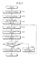
- FIG. 3 is a flowchart for describing the operations of the wireless communication device 10 according to the present embodiment.
- control unit 101 flips the switches 108, 112, and 117 to the "a" sides (step S301). This leads the wireless communication device 10 into a connection state in the correction value calculating mode.
- the modulation processing unit 102 outputs a CW signal as an I channel signal (step S302).
- the control unit 101 sets the reference frequency C of the local signal at the local signal generator 110 (step S303).
- the reference frequency C is preferably set as the central frequency in the transmission bandwidth.
- the reference frequency C is preferably set at 1950 MHz that is the central frequency of the transmission bandwidth from 1920 to 1980 MHz.
- the loop process including steps S304 to S308 is repeated more than once.
- the level detecting unit 119 detects the voltage level (reference level) Vc of the CW signal at the reference frequency C (step S304).
- the control unit 101 determines whether all of the target frequencies n in the transmission bandwidth have been swept or, in other words, whether the correction values have been calculated throughout the transmission bandwidth (step S307).
- the number of the target frequencies n is determined by the shift interval of the frequencies of the local signal. In other words, the smaller the shift interval of the frequencies is, the more the number of the target frequencies n is. Thus, the correction accuracy of the ripple deviation becomes high.
- the shift interval of the frequencies is capable of being set at 100 kHz.
- control unit 101 shifts the frequency of the local signal by a predetermined amount in order to set new target frequency n (step S308).
- step S304 From step S308 in order to conduct the second and subsequent loop processes.
- the level detecting unit 119 detects the voltage level Vn of the CW signal at the target frequency n (step S304).
- the correction value calculating unit 120 calculates the correction value "Vn - Vc" (or, the correction value "Vc - Vn") (step S305) in order to store the calculated correction value in the correction value storing unit 121 (step S306).
- control unit 101 determines whether all of the target frequencies n in the transmission bandwidth have been swept or, in other words, whether the correction values have been calculated throughout the transmission bandwidth (step S307).
- step S307 When all of the target frequencies n in the transmission bandwidth have been swept (step S307: Yes), the control unit 101 flips the switches 108, 112, and 117 to the "b" sides (step S309). This leads the wireless communication device 10 into a connection state in the communication mode.
- the mixer 109 functions as a down-converter in the correction value calculating mode and functions as an up-converter in the communication mode.
- the level detecting unit 119 detects the voltage level of the CW signal that has been up-converted by the mixer 105, has passed through the duplexer 116, and has been down-converted by the mixer 109 in the correction value calculating mode.
- the correction value calculating unit 120 calculates the voltage level correction value of the transmission signal based on the detected voltage level.
- the correction value is updated every time the temperature changes so that the correction value can follow the temperature change.
- the ripple deviation can accurately be corrected.
- the correction value can be updated every time the temperature changes, it is not necessary for the wireless communication device 10 to previously store the correction value corresponded to each temperature.
- the correction value is calculated using the mixer 105 and the mixer 109 that have originally been provided in the wireless communication device 10 for a wireless communication.
- the mixer 109 that has originally been used as only an up-converter also functions as a down-converter using a simple structure in which a switch is flipped.
- the ripple deviation can be corrected with a simple structure while the increase of the device scale is prevented.
- the ripple deviation can accurately be corrected with a simple structure while the increase of the device scale is prevented.
- the mixer 105 and the mixer 109 operate according to the local signal whose frequency is sequentially shifted at predetermined frequency intervals. This can calculate the correction value corresponding to each frequency while sweeping is performed at the predetermined frequency intervals in the transmission bandwidth.
- the ripple deviations can accurately be corrected throughout the transmission bandwidth.
- the signal transmitted from the wireless communication device 10 is a multicarrier signal such as an Orthogonal Frequency-Division Multiplexing (OFDM) signal
- OFDM Orthogonal Frequency-Division Multiplexing
- the correction value at each subcarrier can be obtained so that the ripple deviation can be corrected at each subcarrier.
- the ripple deviations can accurately be corrected in a multicarrier signal.
- an OFDM an Inverse Fast Fourier Transform
- IFFT Inverse Fast Fourier Transform
- the correction value calculating mode when the wireless communication device 10 is not in a communication state, for example, (1) during the initial setup from the activation of the wireless communication device 10 until the wireless communication device 10 becomes available to communicate, (2) when the wireless communication device 10 is in a standby state, and (3) when the wireless communication device 10 is in a Compressed Mode, in addition to the time at the factory shipment of the wireless communication device 10. This can calculate the correction value without interrupting the data communication of the wireless communication device 10.
- the ADC that has originally been provided in the wireless communication device 10 for the RF power detection for an Auto Power Control (APC) of the PA 114 is capable of being used as the ADC 118. This can further prevent the increase of the device scale of the wireless communication device 10.
- APC Auto Power Control
- the mixer 109 that functions as the up-converter for the Q channel signal in the communication mode functions as the down-converter for the CW signal in the correction value calculating mode.
- the mixer 105 that functions as the up-converter for the I channel signal in the communication mode may function as the down-converter for the CW signal in the correction value calculating mode.
- the switch 108 and the switch 112 are provided at both sides of the mixer 105, and the modulation processing unit 102 may generate a CW signal as a Q channel signal in the correction value calculating mode.
- either of two mixers may be used as a down-converter in the correction value calculating mode.
- the above-mentioned wireless communication device 10 is capable of being implemented by the hardware configuration described below.
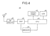
- FIG. 4 is a view for illustrating an exemplary hardware configuration of the wireless communication device 10.
- the wireless communication device 10 includes the antenna 12, a Radio Frequency (RF) circuit 41, a Digital Signal Processor (DSP) 42, a Central Processing Unit (CPU) 43, a memory 44, a touch panel 45, and a Liquid Crystal Display (LCD) 46.
- RF Radio Frequency
- DSP Digital Signal Processor
- CPU Central Processing Unit
- LCD Liquid Crystal Display
- the transmission RF unit 11, the duplexer 116, the switch 117, and the reception RF unit 13 illustrated in FIG. 2 are implemented by the RF circuit 41. Further, the modulation processing unit 102, the level detecting unit 119, the correction value calculating unit 120, the level correcting unit 122, and the demodulation processing unit 131 illustrated in FIG. 2 are implemented by the DSP 42. Further, the control unit 101 illustrated in FIG. 2 is implemented by the CPU 43. Further, the correction value storing unit 121 illustrated in FIG. 2 is implemented by the memory 44.
- the above-mentioned wireless communication device 10 is suitable for a communication terminal.
- a ripple deviation can accurately be corrected with a simple structure while the increase of the device scale is prevented.
Landscapes
- Engineering & Computer Science (AREA)
- Signal Processing (AREA)
- Computer Networks & Wireless Communication (AREA)
- Transmitters (AREA)
- Transceivers (AREA)
Abstract
Description
- The embodiments discussed herein are directed to a wireless communication device.
- It is important to secure a stable throughput with the growing needs for a larger data amount and a faster data transmission in these days. In the 3rd Generation Partnership Project Long Term Evolution (3GPP-LTE) that is a new communication scheme for mobile communications, a channel bandwidth is extended up to 20 MHz. Extension of a channel bandwidth tends to increase the in-band ripple deviation (hereinafter, abbreviated as "ripple deviation") inherent in a high-frequency device such as a duplexer. The increase of the ripple deviation causes reduction of the Error Vector Magnitude (EVM) and thus reduces the throughput.
-
FIG. 1 illustrates an example of frequency characteristics of a duplexer that is used in a wireless communication device mounted on a communication terminal device (hereinafter, abbreviated as "communication terminal") such as a mobile phone. In the example, ripple deviations occur in the transmission bandwidth of 1920 to 1980 MHz. The ripple deviations vary depending on each individual duplexer due to the temperature change, the variation in the elements, the difference of manufacturers, the difference of models even in the same manufacture, or the like. It is difficult to further improve the performance of the duplexer itself in order to reduce the ripple deviations because it increases the production cost. - Conventionally, to reduce the effect of ripple deviations to a transmission signal, a technique for previously correcting the voltage level of the transmission signal before being input to the duplexer with a correction value for negating the ripple deviation (hereinafter, abbreviated as "correction value") has been used. Conventionally, based on the correction values for as many wireless communication devices as possible, the average value of the correction values is stored in the memories of wireless communication devices as the correction value of the individual wireless communication device at the experimental stage of a wireless communication device. Then, when the wireless communication is in a communication state, the correction value stored in the memory corrects the voltage level of the transmission signal.
- Related-art examples are described, for example, in Japanese Laid-open Patent Publication No.
2004-235966 2006-186690 - Because the correction value stored in the memory at the experimental stage of a wireless communication device as described above is a fixed value, it is difficult to follow the temperature change. On the contrary, when the correction values according to the temperatures are stored in the memory in consideration of the temperature change, the storage capacity of the memory becomes large and thus the device scale of the wireless communication device becomes large. Further, in this case, since it is preferable to detect the temperature of the wireless communication device, the device structure of the wireless communication device becomes complicated. Further, because the correction value stored in the memory is conventionally an average value of a plurality of wireless communication devices, it is difficult to completely correct the ripple deviations that are different from each other at each duplexer.
- Accordingly, it is an object in one aspect of an embodiment of the invention to provide a wireless communication device that is capable of accurately correcting a ripple deviation with a simple structure while preventing the increase of the device scale.
- According to an aspect of an embodiment, a wireless communication device includes an antenna, a duplexer that allows the antenna to be used as both of a transmitting antenna and a receiving antenna, a first mixer that functions as an up-converter, a second mixer that functions as a down-converter in a first mode, and functions as an up-converter in a second mode, a detecting unit that detects a level of a signal that has been up-converted by the first mixer, has passed through the duplexer, and has been down-converted by the second mixer in the first mode, and a calculating unit that calculates a level correction value of a transmission signal based on the detected level.
-
-
FIG. 1 is a view illustrating an example of frequency characteristics of a duplexer; -
FIG. 2 is a view illustrating an exemplary structure of a wireless communication device according to an embodiment; -
FIG. 3 is a flowchart for describing the operations of the wireless communication device according to the embodiment; and -
FIG. 4 is a view illustrating an exemplary hardware configuration of the wireless communication device. -
FIG. 2 is a view illustrating an exemplary structure of awireless communication device 10 according to the present embodiment. InFIG. 2 , thewireless communication device 10 includes acontrol unit 101, amodulation processing unit 102, a transmission Radio Frequency (RF)unit 11, aduplexer 116, aswitch 117, anantenna 12, a reception Radio Frequency (RF)unit 13, a demodulation processing unit 131, alevel detecting unit 119, a correctionvalue calculating unit 120, a correctionvalue storing unit 121, and alevel correcting unit 122. Further, thetransmission RF unit 11 includes Digital to Analog Converters (DACs) 103 and 106, Low-Pass Filters (LPFs) 104 and 107, alocal signal generator 110, a π/2phase shifter 111,mixers switches combiner 113, a Power Amplifier (PA) 114, an Isolator (ISO) 115, and an Analog to Digital Converter (ADC) 118. Further, themixers local signal generator 110, the π/2phase snifter 111, and the combiner 113 form a quadrature modulator. - The
wireless communication device 10 operates in either of a first mode or a second mode. The first mode is for calculating a correction value for correcting the voltage level of a transmission signal (hereinafter, referred to as the "correction value calculating mode"). The second mode is for transmitting and receiving a signal through an antenna (hereinafter, referred to as the "communication mode"). In the correction value calculating mode, thecontrol unit 101 flips theswitches control unit 101 flips theswitches - First, the correction value calculating mode will be described.
- The
control unit 101 flips theswitches duplexer 116 to themixer 109, and connects themixer 109 to the ADC 118, so that thewireless communication device 10 gets into a connection state in the correction value calculating mode. Thecontrol unit 101 further controls the frequency of a local signal generated by thelocal signal generator 110. Thecontrol unit 101 makes the frequency of the local signal sweep in the transmission bandwidth. - The
modulation processing unit 102 generates a Continuous Wave (CW) signal (for example, a sine curve signal of 1 MHz) as an I channel signal and outputs the generated CW signal to theDAC 103. On the other hand, themodulation processing unit 102 does not generate and output a Q channel signal. Thus, in the correction value calculating mode, theDAC 106 and theLPF 107 do not operate, and the signal is input to thecombiner 113 only from themixer 105, and not from themixer 109. - The
DAC 103 converts a digital CW signal into an analog CW signal and outputs the converted CW signal to theLPF 104. - The
LPF 104 eliminates the high-frequency component from the CW signal and outputs the CW signal that has only the low-frequency component to themixer 105. - The
local signal generator 110 generates a local signal according to the frequency control from thecontrol unit 101 and outputs the generated local signal to the π/2phase shifter 111. - The π/2 phase snifter 111 shifts, by π/2, the phase of one of the local signals that are to be output to the
mixer 105 and themixer 109 so that the difference between the phases of the I channel signal and the Q channel signal becomes π/2. For example, the π/2phase shifter 111 shifts, by π/2, only the phase of the local signal that is to be output to themixer 109 in order to make the difference between the phases of the I channel signal and the Q channel signal π/2. - The
mixer 105 mixes the CW signal input from theLPF 104 with the local signal input from the π/2phase snifter 111. This gets a CW signal up-converted by the local signal and a CW signal down-converted by the local signal, and the CW signals are output to thecombiner 113. - Here, the
PA 114, the ISO 115, and theduplexer 116 are elements that work for high-frequency signals and do not work for low-frequency signals. Thus, thePA 114, the ISO 115, and theduplexer 116 work only for the up-converted CW signal among the CW signals obtained by themixer 105. In other words, in thewireless communication device 10, themixer 105 functions as an up-converter. Further, themixer 105 functions as an up-converter in both of the correction value calculating mode and the communication mode. - The CW signal that has been input to the
combiner 113 is input to thePA 114 through thecombiner 113. - The
PA 114 amplifies the Radio Frequency (RF) power of the CW signal and outputs the power-amplified CW signal to the ISO 115, The power-amplified CW signal is input to themixer 109 through the ISO 115, theduplexer 116, theswitch 117, and theswitch 108. - The
mixer 109 mixes the CW signal that is output from thePA 114 and is input through the ISO 115, theduplexer 116, theswitch 117, and theswitch 108 with the CW signal that is input from the π/2phase shifter 111. Accordingly, a CW signal up-converted by the local signal and a CW signal down-converted by the local signal are obtained, and these CW signals are output to theADC 118 through theswitch 112. - Here, the ADC 118 is an element that works for low-frequency signals and does not work for high-frequency signals. Thus, the
ADC 118 works only for the down-converted CW signal among the CW signals obtained by themixer 109. In other words, in the correction value calculating mode, themixer 105 functions as a down-converter in thewireless communication device 10. - The
ADC 118 converts an analog CW signal into a digital CW signal and outputs the converted CW signal to thelevel detecting unit 119. - Here, because the signal input to the
level detecting unit 119 has been input through theduplexer 116, the signal becomes a CW signal having the ripple deviations as illustrated inFIG. 1 . - The
level detecting unit 119 detects the voltage level of the input CW signal and outputs the detection result to the correctionvalue calculating unit 120. In other words, thelevel detecting unit 119 detects the voltage level of the CW signal that has been up-converted in themixer 105, has passed through theduplexer 116, and then has been down-converted in themixer 109. - The correction
value calculating unit 120 calculates a correction value based on the voltage level detected in thelevel detecting unit 119, and stores the calculated correction value in the correctionvalue storing unit 121. - In the correction value calculating mode, the
control unit 101 sequentially shifts the frequency of thelocal signal generator 110 at predetermined frequency intervals in order to perform the above-mentioned series of processes. In other words, themixer 105 and themixer 109 operate according to the local signal whose frequency is sequentially shifted at predetermined frequency intervals. Accordingly, a plurality of the correction values for the ripple deviations at a plurality of frequency points are stored in the correctionvalue storing unit 121. - The correction
value calculating unit 120 calculates, as the correction value, the difference "Vn - Vc" between a voltage level (reference level) Vc of a predetermined reference frequency C in the transmission bandwidth and a voltage level Vn at a target frequency n in the transmission bandwidth. The target frequency n is a frequency to be targeted for the calculation of correction value. The target frequencies n are a plurality of frequency points in the transmission bandwidth, and correspond to, for example, some of frequency points from 1920 to 1980 MHz in the example illustrated inFIG. 1 . Note that, the correctionvalue calculating unit 120 may also calculate "Vc - Vn" as the correction value. - Next, the communication mode will be described.
- The
control unit 101 flips theswitches LPF 107 to themixer 109, connects themixer 109 to thecombiner 113, and connects theduplexer 116 and theantenna 12, so that thewireless communication device 10 gets into a connection state in the communication mode. Thecontrol unit 101 further controls the frequency of the local signal generated by thelocal signal generator 110. Thecontrol unit 101 sets one of the frequencies used for a communication in the transmission bandwidth as the frequency of the local signal. Thecontrol unit 101 further outputs a signal indicating the frequency of the local signal (or, namely, a signal indicating the transmission frequency) to thelevel correcting unit 122. - The
level correcting unit 122 corrects the voltage level of the input transmission signal using the correction value stored in the correctionvalue storing unit 121 in order to output the corrected transmission signal to themodulation processing unit 102. Thelevel correcting unit 122 adds, to the voltage level of the transmission signal, the correction value "Vn - Vc" corresponding to the transmission frequency n indicated by thecontrol unit 101 in order to correct the voltage level of the transmission signal. Note that, when the correctionvalue calculating unit 120 calculates the "Vc - Vn" as the correction value, thelevel correcting unit 122 subtracts the correction value "Vc - Vn" from the voltage level of the transmission signal in order to correct the voltage level of the transmission signal. As described above, using the correction value, previously correcting the voltage level of the transmission signal before being input to theduplexer 116 negates the ripple deviation of the transmission signal when the transmission signal passes through theduplexer 116. - The
modulation processing unit 102 modulates the transmission signal after the level has been corrected in order to generate an I channel signal and a Q channel signal. Themodulation processing unit 102 outputs the I channel signal to theDAC 103, and outputs the Q channel signal to theDAC 106. - The
DAC 103 converts the digital I channel signal into the analog I channel signal and outputs the converted I channel signal to theLPF 104. - The
LPF 104 eliminates the high-frequency component from the I channel signal in order to output the I channel signal that has only the low-frequency component to themixer 105. - The
DAC 106 converts the digital Q channel signal into the analog Q channel signal and outputs the converted Q channel signal to theLPF 107. - The
LPF 107 eliminates the high-frequency component from the Q channel signal in order to output the Q channel signal that has only the low-frequency component to themixer 109 through theswitch 108. - The
local signal generator 110 generates the local signal having the frequency set by thecontrol unit 101 in order to output the generated local signal to the π/2phase shifter 111. - The
mixer 105 mixes the I channel signal input from theLPF 104 with the local signal input from the π/2phase shifter 111. Accordingly, an I channel signal up-converted by the local signal and an I channel signal down-converted by the local signal are obtained, and the I channel signals are output to thecombiner 113. - Here, the
mixer 105 functions as an up-converter in both of the correction value calculating mode and the communication mode as described above. - On the other hand, the
mixer 109 mixes the Q channel signal input from theLPF 107 with the local signal input from the π/2phase snifter 111. Accordingly, a Q channel signal up-converted by the local signal and a Q channel signal down-converted by the local signal are obtained, and the Q channel signals are output to thecombiner 113 through theswitch 112. - Here, as described above, the
PA 114, theISO 115, and theduplexer 116 are elements that work for high-frequency signals and do not work for low-frequency signals. Thus, thePA 114, theISO 115, and theduplexer 116 work only for the up-converted Q channel signal among the Q channel signals obtained by themixer 109. In other words, in the communication mode, themixer 109 functions as an up-converter in thewireless communication device 10. - The phase of the I channel signal output from the
mixer 105 differs from the phase of the Q channel signal output from themixer 109 by π/2. - The
combiner 113 combines the I channel signal and the Q channel signal in order to generate a combined signal and outputs the generated combined signal to thePA 114. - The
PA 114 amplifies the RF power of the combined signal in order to output the power-amplified combined signal to theISO 115. The power-amplified combined signal is transmitted from thewireless communication device 10 through theISO 115, theduplexer 116, theswitch 117, and theantenna 12. - On the other hand, the signal that has been received through the
antenna 12, theswitch 117, and theduplexer 116 is input to thereception RF unit 13. - In other words, the
duplexer 116 is for using theantenna 12 as both of a transmitting antenna and a receiving antenna. - The
reception RF unit 13 performs a receiving process including a down-conversion and an A/D conversion on the input analog received signal in order to output the digital received signal after the receiving process to the demodulation processing unit 131. - The demodulation processing unit 131 demodulates the digital received signal in order to output the demodulated received signal.
-
FIG. 3 is a flowchart for describing the operations of thewireless communication device 10 according to the present embodiment. - First, the
control unit 101 flips theswitches wireless communication device 10 into a connection state in the correction value calculating mode. - Next, the
modulation processing unit 102 outputs a CW signal as an I channel signal (step S302). - Next, the
control unit 101 sets the reference frequency C of the local signal at the local signal generator 110 (step S303). The reference frequency C is preferably set as the central frequency in the transmission bandwidth. For example, when theduplexer 116 has the frequency characteristic illustrated inFIG. 1 , the reference frequency C is preferably set at 1950 MHz that is the central frequency of the transmission bandwidth from 1920 to 1980 MHz. - Here, the loop process including steps S304 to S308 is repeated more than once.
- In other words, at the first loop process, the
level detecting unit 119 detects the voltage level (reference level) Vc of the CW signal at the reference frequency C (step S304). - Next, the correction
value calculating unit 120 calculates the correction value (step S305), and stores the calculated correction value in the correction value storing unit 121 (step S306). Because of Vc = Vn at the first loop process, the correction value at the reference frequency C is zero. Further, at the first loop process, the correctionvalue calculating unit 120 maintains the reference level Vc. - Next, the
control unit 101 determines whether all of the target frequencies n in the transmission bandwidth have been swept or, in other words, whether the correction values have been calculated throughout the transmission bandwidth (step S307). The number of the target frequencies n is determined by the shift interval of the frequencies of the local signal. In other words, the smaller the shift interval of the frequencies is, the more the number of the target frequencies n is. Thus, the correction accuracy of the ripple deviation becomes high. For example, the shift interval of the frequencies is capable of being set at 100 kHz. - When all of the target frequencies n in the transmission bandwidth have not been swept (step S307: No), the
control unit 101 shifts the frequency of the local signal by a predetermined amount in order to set new target frequency n (step S308). - Then, the process goes back to step S304 from step S308 in order to conduct the second and subsequent loop processes.
- At the second and subsequent loop processes, the
level detecting unit 119 detects the voltage level Vn of the CW signal at the target frequency n (step S304). - Next, the correction
value calculating unit 120 calculates the correction value "Vn - Vc" (or, the correction value "Vc - Vn") (step S305) in order to store the calculated correction value in the correction value storing unit 121 (step S306). - Next, the
control unit 101 determines whether all of the target frequencies n in the transmission bandwidth have been swept or, in other words, whether the correction values have been calculated throughout the transmission bandwidth (step S307). - When all of the target frequencies n in the transmission bandwidth have been swept (step S307: Yes), the
control unit 101 flips theswitches wireless communication device 10 into a connection state in the communication mode. - After that, the process described in the above-mentioned item <Communication mode> is conducted.
- In the present embodiment as described above, in the
wireless communication device 10, while themixer 105 functions as an up-converter in both of the correction value calculating mode and the communication mode, themixer 109 functions as a down-converter in the correction value calculating mode and functions as an up-converter in the communication mode. Further, thelevel detecting unit 119 detects the voltage level of the CW signal that has been up-converted by themixer 105, has passed through theduplexer 116, and has been down-converted by themixer 109 in the correction value calculating mode. The correctionvalue calculating unit 120 calculates the voltage level correction value of the transmission signal based on the detected voltage level. - This can properly update the correction value even after the beginning of use of a wireless communication device by setting the wireless communication device at the correction value calculating mode, so that the correction value can be kept appropriate. For example, the correction value is updated every time the temperature changes so that the correction value can follow the temperature change. Thus, according to the present embodiment, even if the temperature has changed, the ripple deviation can accurately be corrected.
- Further, according to the present embodiment, because the correction value can be updated every time the temperature changes, it is not necessary for the
wireless communication device 10 to previously store the correction value corresponded to each temperature. Further, according to the present embodiment, the correction value is calculated using themixer 105 and themixer 109 that have originally been provided in thewireless communication device 10 for a wireless communication. Further, according to the present embodiment, themixer 109 that has originally been used as only an up-converter also functions as a down-converter using a simple structure in which a switch is flipped. Thus, according to the present embodiment, the ripple deviation can be corrected with a simple structure while the increase of the device scale is prevented. - In other words, according to the present embodiment, the ripple deviation can accurately be corrected with a simple structure while the increase of the device scale is prevented.
- Further, according to the present embodiment, the
mixer 105 and themixer 109 operate according to the local signal whose frequency is sequentially shifted at predetermined frequency intervals. This can calculate the correction value corresponding to each frequency while sweeping is performed at the predetermined frequency intervals in the transmission bandwidth. Thus, according to the present embodiment, the ripple deviations can accurately be corrected throughout the transmission bandwidth. - Note that, when the signal transmitted from the
wireless communication device 10 is a multicarrier signal such as an Orthogonal Frequency-Division Multiplexing (OFDM) signal, it is preferable to shift the frequency of the local signal at subcarrier intervals of a plurality of subcarriers included in the multicarrier signal. The correction value at each subcarrier can be obtained so that the ripple deviation can be corrected at each subcarrier. Thus, the ripple deviations can accurately be corrected in a multicarrier signal. When the signal transmitted from thewireless communication device 10 is an OFDM signal, an Inverse Fast Fourier Transform (IFFT) process is further performed on the level-corrected transmission signal in themodulation processing unit 102. - Further, it is preferable to perform the correction value calculating mode when the
wireless communication device 10 is not in a communication state, for example, (1) during the initial setup from the activation of thewireless communication device 10 until thewireless communication device 10 becomes available to communicate, (2) when thewireless communication device 10 is in a standby state, and (3) when thewireless communication device 10 is in a Compressed Mode, in addition to the time at the factory shipment of thewireless communication device 10. This can calculate the correction value without interrupting the data communication of thewireless communication device 10. - Further, the ADC that has originally been provided in the
wireless communication device 10 for the RF power detection for an Auto Power Control (APC) of thePA 114 is capable of being used as theADC 118. This can further prevent the increase of the device scale of thewireless communication device 10. - Further, according to the present embodiment, the
mixer 109 that functions as the up-converter for the Q channel signal in the communication mode functions as the down-converter for the CW signal in the correction value calculating mode. Themixer 105 that functions as the up-converter for the I channel signal in the communication mode, however, may function as the down-converter for the CW signal in the correction value calculating mode. In that case, theswitch 108 and theswitch 112 are provided at both sides of themixer 105, and themodulation processing unit 102 may generate a CW signal as a Q channel signal in the correction value calculating mode. In other words, either of two mixers may be used as a down-converter in the correction value calculating mode. - The above-mentioned
wireless communication device 10 is capable of being implemented by the hardware configuration described below. -
FIG. 4 is a view for illustrating an exemplary hardware configuration of thewireless communication device 10. As illustrated inFIG. 4 , as for the hardware, thewireless communication device 10 includes theantenna 12, a Radio Frequency (RF)circuit 41, a Digital Signal Processor (DSP) 42, a Central Processing Unit (CPU) 43, amemory 44, atouch panel 45, and a Liquid Crystal Display (LCD) 46. - The
transmission RF unit 11, theduplexer 116, theswitch 117, and thereception RF unit 13 illustrated inFIG. 2 are implemented by theRF circuit 41. Further, themodulation processing unit 102, thelevel detecting unit 119, the correctionvalue calculating unit 120, thelevel correcting unit 122, and the demodulation processing unit 131 illustrated inFIG. 2 are implemented by theDSP 42. Further, thecontrol unit 101 illustrated inFIG. 2 is implemented by theCPU 43. Further, the correctionvalue storing unit 121 illustrated inFIG. 2 is implemented by thememory 44. - Hereinabove, the embodiments of the present invention have been described.
- Note that, the above-mentioned
wireless communication device 10 is suitable for a communication terminal. - According to the above-mentioned embodiment of the wireless communication device disclosed in the present invention, a ripple deviation can accurately be corrected with a simple structure while the increase of the device scale is prevented.
Claims (4)
- A wireless communication device (10) comprising:an antenna (12);a duplexer (116) that allows the antenna (10) to be used as both of a transmitting antenna and a receiving antenna;a first mixer (105) that functions as an up-converter;a second mixer (109) that functions as a down-converter in a first mode, and functions as an up-converter in a second mode;a detecting unit (119) that detects a level of signal that has been up-converted by the first mixer (105), has passed through the duplexer (116), and has been down-converted by the second mixer (109) in the first mode; anda calculating unit (120) that calculates a level correction value of a transmission signal based on the detected level.
- The wireless communication device (10) according to claim 1, wherein the first mixer (105) and the second mixer (109) operate according to a local signal whose frequency is sequentially shifted at predetermined frequency intervals throughout a transmission bandwidth in the first mode.
- The wireless communication device according to claim 2, wherein the predetermined frequency interval is a subcarrier interval of a plurality of subcarriers included in a multicarrier signal.
- The wireless communication device according to any one of claims 1 to 3, wherein the calculating unit (120) calculates the level correction value when the wireless communication device (10) is not in a communication state.
Applications Claiming Priority (1)
| Application Number | Priority Date | Filing Date | Title |
|---|---|---|---|
| JP2012077825A JP5825175B2 (en) | 2012-03-29 | 2012-03-29 | Wireless communication device |
Publications (4)
| Publication Number | Publication Date |
|---|---|
| EP2645581A2 true EP2645581A2 (en) | 2013-10-02 |
| EP2645581A3 EP2645581A3 (en) | 2014-09-03 |
| EP2645581B1 EP2645581B1 (en) | 2016-10-19 |
| EP2645581B8 EP2645581B8 (en) | 2017-05-24 |
Family
ID=47561138
Family Applications (1)
| Application Number | Title | Priority Date | Filing Date |
|---|---|---|---|
| EP12197667.4A Not-in-force EP2645581B8 (en) | 2012-03-29 | 2012-12-18 | Wireless communication device |
Country Status (4)
| Country | Link |
|---|---|
| US (1) | US8982740B2 (en) |
| EP (1) | EP2645581B8 (en) |
| JP (1) | JP5825175B2 (en) |
| KR (1) | KR101468281B1 (en) |
Cited By (1)
| Publication number | Priority date | Publication date | Assignee | Title |
|---|---|---|---|---|
| CN114499573A (en) * | 2022-03-01 | 2022-05-13 | 福建科立讯通信有限公司 | Terminal wireless communication method, device and medium for adaptive switching of private network modulus |
Citations (2)
| Publication number | Priority date | Publication date | Assignee | Title |
|---|---|---|---|---|
| JP2004235966A (en) | 2003-01-30 | 2004-08-19 | Seiko Epson Corp | Wireless communication device |
| JP2006186690A (en) | 2004-12-27 | 2006-07-13 | Nec Corp | Radio transmission device and transmission power adjustment method thereof |
Family Cites Families (41)
| Publication number | Priority date | Publication date | Assignee | Title |
|---|---|---|---|---|
| US4275398A (en) * | 1979-04-06 | 1981-06-23 | Del Norte Technology, Inc. | FM Radio ranging system |
| JPS58212646A (en) * | 1982-06-04 | 1983-12-10 | Hitachi Ltd | Variable speed playback device for magnetic recording and playback device |
| US4520508A (en) * | 1982-12-21 | 1985-05-28 | General Instrument Corporation | Subscriber terminal for monitoring radio-frequency signal ingress into cable television systems |
| EP0500373B1 (en) * | 1991-02-22 | 1998-04-29 | Sony Corporation | Time division duplex transmitter-receiver |
| US5524285A (en) * | 1993-11-02 | 1996-06-04 | Wray; Anthony J. | Radio transmitter with power amplifier and linearization |
| US6243399B1 (en) * | 1994-07-21 | 2001-06-05 | Interdigital Technology Corporation | Ring signal generator |
| GB2301247A (en) * | 1995-05-22 | 1996-11-27 | Univ Bristol | A cartesian loop transmitter amplifier |
| US6253060B1 (en) * | 1996-12-20 | 2001-06-26 | Airnet Communications Corporation | Method and apparatus employing wireless remote loopback capability for a wireless system repeater to provide end-to-end testing without a wireline connection |
| JP2000151317A (en) * | 1998-11-10 | 2000-05-30 | Hitachi Ltd | Transmitter and power amplifier |
| US6272329B1 (en) * | 1998-12-09 | 2001-08-07 | Nortel Networks Limited | Bidirectional frequency translator and full duplex transceiver system employing same |
| JP3618055B2 (en) * | 1999-02-05 | 2005-02-09 | 富士通株式会社 | Portable mobile terminal and transmitter |
| US7555263B1 (en) * | 1999-10-21 | 2009-06-30 | Broadcom Corporation | Adaptive radio transceiver |
| KR100672396B1 (en) * | 1999-12-28 | 2007-01-23 | 엘지전자 주식회사 | Post Service Method of Mobile Terminal |
| JP2002208858A (en) * | 2001-01-10 | 2002-07-26 | Matsushita Electric Ind Co Ltd | Frequency synthesizer and frequency generation method |
| US7634243B1 (en) * | 2002-06-19 | 2009-12-15 | Microtune (Texas), L.P. | System and method for providing a dual conversion tuner having a first IF filter without fixed center frequency |
| GB2390495A (en) * | 2002-07-05 | 2004-01-07 | Motorola Inc | Calibration of a transmitter or receiver in a transceiver wherein transmitter signals may be detected via the receiver or a separate detection arrangement |
| US7542733B1 (en) * | 2003-02-04 | 2009-06-02 | Sprint Spectrum L.P. | Method and apparatus for diversity transmission from a mobile station |
| KR100602642B1 (en) * | 2004-01-30 | 2006-07-19 | 삼성전자주식회사 | Phase Error Correction Device and Method in Wireless Base Station System |
| US7107022B1 (en) * | 2005-03-04 | 2006-09-12 | Impinj, Inc. | Single RF oscillator single-side band modulation for RFID readers using tone insertion during reader reception |
| JP2006261793A (en) | 2005-03-15 | 2006-09-28 | Matsushita Electric Ind Co Ltd | Transmitter-receiver |
| US20070082617A1 (en) * | 2005-10-11 | 2007-04-12 | Crestcom, Inc. | Transceiver with isolation-filter compensation and method therefor |
| JP5386061B2 (en) * | 2006-05-17 | 2014-01-15 | 株式会社アドバンテスト | Frequency component measuring device |
| US7688880B2 (en) * | 2006-05-31 | 2010-03-30 | Spreadtrum Communications Inc. | Method and apparatus for reduced noise and carrier feedthrough in multimode transmitter |
| US7783263B2 (en) * | 2006-12-14 | 2010-08-24 | Texas Instruments Incorporated | Simplified digital predistortion in a time-domain duplexed transceiver |
| WO2008091556A1 (en) * | 2007-01-24 | 2008-07-31 | Powerwave Technologies, Inc. | Adaptive echo cancellation for an on-frequency rf repeater using a weighted power spectrum |
| US8805298B2 (en) * | 2007-01-30 | 2014-08-12 | Crestcom, Inc. | Transceiver with compensation for transmit signal leakage and method therefor |
| US20090268784A1 (en) * | 2007-07-12 | 2009-10-29 | Focus Enhancements, Inc. | Multi-band ofdm receiver |
| US8442456B2 (en) * | 2007-08-09 | 2013-05-14 | Freescale Semiconductor, Inc. | Wireless communication unit, integrated circuit and method of power control therein |
| US7929917B1 (en) * | 2007-12-21 | 2011-04-19 | Nortel Networks Limited | Enhanced wideband transceiver |
| US7994870B2 (en) * | 2008-10-20 | 2011-08-09 | Qualcomm, Incorporated | Tunable filter with gain control circuit |
| US8243851B2 (en) * | 2009-04-01 | 2012-08-14 | Ubidyne, Inc. | Radio system and a method for relaying radio signals |
| US9559639B2 (en) * | 2009-08-19 | 2017-01-31 | Qualcomm Incorporated | Protection circuit for power amplifier |
| RU2012112544A (en) * | 2009-08-31 | 2013-10-10 | Хуавэй Текнолоджиз Ко., Лтд. | METHOD AND DEVICE FOR DUPLEXER FAULT FINDING |
| CN102035932B (en) * | 2009-09-24 | 2013-02-13 | 鸿富锦精密工业(深圳)有限公司 | Mobile phone having maximum power calibrating function |
| US8542768B2 (en) * | 2009-12-21 | 2013-09-24 | Dali Systems Co. Ltd. | High efficiency, remotely reconfigurable remote radio head unit system and method for wireless communications |
| US8358170B2 (en) * | 2010-03-23 | 2013-01-22 | Intersil Americas Inc. | Power amplifier linearization using cancellation-based feed forward methods and systems |
| US8774874B2 (en) * | 2010-06-04 | 2014-07-08 | Qualcomm Incorporated | Reducing power consumption by in-circuit measurement of receive band attenuation and/or noise |
| JP2012039560A (en) | 2010-08-11 | 2012-02-23 | Kyocera Corp | Wireless base station apparatus |
| US8660057B2 (en) * | 2010-08-26 | 2014-02-25 | Golba, Llc | Method and system for distributed communication |
| US8912963B2 (en) * | 2010-10-20 | 2014-12-16 | Apple Inc. | System for testing multi-antenna devices using bidirectional faded channels |
| US9154240B2 (en) * | 2011-08-18 | 2015-10-06 | Qualcomm Incorporated | Precision power/peak detector using on-chip reference power source |
-
2012
- 2012-03-29 JP JP2012077825A patent/JP5825175B2/en not_active Expired - Fee Related
- 2012-12-18 EP EP12197667.4A patent/EP2645581B8/en not_active Not-in-force
- 2012-12-18 US US13/718,408 patent/US8982740B2/en not_active Expired - Fee Related
- 2012-12-26 KR KR1020120153535A patent/KR101468281B1/en not_active Expired - Fee Related
Patent Citations (2)
| Publication number | Priority date | Publication date | Assignee | Title |
|---|---|---|---|---|
| JP2004235966A (en) | 2003-01-30 | 2004-08-19 | Seiko Epson Corp | Wireless communication device |
| JP2006186690A (en) | 2004-12-27 | 2006-07-13 | Nec Corp | Radio transmission device and transmission power adjustment method thereof |
Cited By (1)
| Publication number | Priority date | Publication date | Assignee | Title |
|---|---|---|---|---|
| CN114499573A (en) * | 2022-03-01 | 2022-05-13 | 福建科立讯通信有限公司 | Terminal wireless communication method, device and medium for adaptive switching of private network modulus |
Also Published As
| Publication number | Publication date |
|---|---|
| JP5825175B2 (en) | 2015-12-02 |
| US8982740B2 (en) | 2015-03-17 |
| KR101468281B1 (en) | 2014-12-03 |
| JP2013207756A (en) | 2013-10-07 |
| US20130258910A1 (en) | 2013-10-03 |
| EP2645581B1 (en) | 2016-10-19 |
| EP2645581B8 (en) | 2017-05-24 |
| EP2645581A3 (en) | 2014-09-03 |
| KR20130111192A (en) | 2013-10-10 |
Similar Documents
| Publication | Publication Date | Title |
|---|---|---|
| US20110051790A1 (en) | Radio communication device and method | |
| CN106803775A (en) | For the apparatus and method of transceiver calibration | |
| US20160056903A1 (en) | System, method and computer storage medium for calibrating RF transceiver | |
| US8224268B2 (en) | Transmitter linearization | |
| US9137069B2 (en) | Systems and methods to frequency shift unwanted signal components | |
| US10330775B2 (en) | Transmitter, transmission method, phase adjustment device, and phase adjustment method | |
| EP4016947A1 (en) | Digital pre-distortion (dpd) estimation window search | |
| US20190158325A1 (en) | Carrier leakage correction method for quadrature modulator | |
| CN102647373B (en) | Method and device for correcting unmatching of same phase/orthogonal signals in communication circuit | |
| EP2645581B1 (en) | Wireless communication device | |
| US8559553B2 (en) | Transmitter apparatus | |
| KR102170631B1 (en) | A Signal Processing Method for Improving the Resolution of a Stepped Frequency Broadband Radar Using a Direct Conversion Method RF Chip | |
| US20130034185A1 (en) | Wireless communication device and wireless communication method | |
| JP2009060174A (en) | Wireless device, wireless circuit, and wireless circuit control method | |
| JP2010233058A (en) | Narrow band digital radio communication system and radio set | |
| US20200106657A1 (en) | Signal imbalance detection systems and methods | |
| US10063368B2 (en) | Phase locked loop circuit, RF front-end circuit, wireless transmission/reception circuit, and mobile wireless communication terminal apparatus | |
| JP6709454B2 (en) | Phase synchronization circuit, RF front-end circuit, wireless transmission/reception circuit, portable wireless communication terminal device | |
| JP2012039560A (en) | Wireless base station apparatus | |
| US12429829B2 (en) | Digital-to-time converter (DTC) non-linearity predistortion | |
| JP2012227867A (en) | Radio communication apparatus | |
| JP5752005B2 (en) | Transmitter | |
| KR20120054773A (en) | Apparatus and method for calibration in wireless comunication system | |
| JP2014195156A (en) | Receiving device, reception method, transmission and reception device, transmission and reception method | |
| JP2008098781A (en) | Communication device |
Legal Events
| Date | Code | Title | Description |
|---|---|---|---|
| PUAI | Public reference made under article 153(3) epc to a published international application that has entered the european phase |
Free format text: ORIGINAL CODE: 0009012 |
|
| AK | Designated contracting states |
Kind code of ref document: A2 Designated state(s): AL AT BE BG CH CY CZ DE DK EE ES FI FR GB GR HR HU IE IS IT LI LT LU LV MC MK MT NL NO PL PT RO RS SE SI SK SM TR |
|
| AX | Request for extension of the european patent |
Extension state: BA ME |
|
| PUAL | Search report despatched |
Free format text: ORIGINAL CODE: 0009013 |
|
| AK | Designated contracting states |
Kind code of ref document: A3 Designated state(s): AL AT BE BG CH CY CZ DE DK EE ES FI FR GB GR HR HU IE IS IT LI LT LU LV MC MK MT NL NO PL PT RO RS SE SI SK SM TR |
|
| AX | Request for extension of the european patent |
Extension state: BA ME |
|
| RIC1 | Information provided on ipc code assigned before grant |
Ipc: H04B 17/00 20060101ALI20140728BHEP Ipc: H04B 1/04 20060101AFI20140728BHEP |
|
| 17P | Request for examination filed |
Effective date: 20150128 |
|
| RBV | Designated contracting states (corrected) |
Designated state(s): AL AT BE BG CH CY CZ DE DK EE ES FI FR GB GR HR HU IE IS IT LI LT LU LV MC MK MT NL NO PL PT RO RS SE SI SK SM TR |
|
| GRAP | Despatch of communication of intention to grant a patent |
Free format text: ORIGINAL CODE: EPIDOSNIGR1 |
|
| INTG | Intention to grant announced |
Effective date: 20160506 |
|
| GRAS | Grant fee paid |
Free format text: ORIGINAL CODE: EPIDOSNIGR3 |
|
| GRAA | (expected) grant |
Free format text: ORIGINAL CODE: 0009210 |
|
| AK | Designated contracting states |
Kind code of ref document: B1 Designated state(s): AL AT BE BG CH CY CZ DE DK EE ES FI FR GB GR HR HU IE IS IT LI LT LU LV MC MK MT NL NO PL PT RO RS SE SI SK SM TR |
|
| REG | Reference to a national code |
Ref country code: GB Ref legal event code: FG4D |
|
| REG | Reference to a national code |
Ref country code: CH Ref legal event code: EP |
|
| RIN2 | Information on inventor provided after grant (corrected) |
Inventor name: OTA, MUTSUHITO Inventor name: NAGAYA, SETSUYA Inventor name: NAKATA, YOUJI Inventor name: KAKIZAKI, SHINJI |
|
| REG | Reference to a national code |
Ref country code: AT Ref legal event code: REF Ref document number: 839103 Country of ref document: AT Kind code of ref document: T Effective date: 20161115 |
|
| REG | Reference to a national code |
Ref country code: IE Ref legal event code: FG4D |
|
| REG | Reference to a national code |
Ref country code: DE Ref legal event code: R096 Ref document number: 602012024274 Country of ref document: DE Ref country code: FR Ref legal event code: PLFP Year of fee payment: 5 |
|
| REG | Reference to a national code |
Ref country code: DE Ref legal event code: R083 Ref document number: 602012024274 Country of ref document: DE |
|
| REG | Reference to a national code |
Ref country code: NL Ref legal event code: MP Effective date: 20161019 |
|
| REG | Reference to a national code |
Ref country code: LT Ref legal event code: MG4D |
|
| PG25 | Lapsed in a contracting state [announced via postgrant information from national office to epo] |
Ref country code: LV Free format text: LAPSE BECAUSE OF FAILURE TO SUBMIT A TRANSLATION OF THE DESCRIPTION OR TO PAY THE FEE WITHIN THE PRESCRIBED TIME-LIMIT Effective date: 20161019 |
|
| REG | Reference to a national code |
Ref country code: AT Ref legal event code: MK05 Ref document number: 839103 Country of ref document: AT Kind code of ref document: T Effective date: 20161019 |
|
| PG25 | Lapsed in a contracting state [announced via postgrant information from national office to epo] |
Ref country code: GR Free format text: LAPSE BECAUSE OF FAILURE TO SUBMIT A TRANSLATION OF THE DESCRIPTION OR TO PAY THE FEE WITHIN THE PRESCRIBED TIME-LIMIT Effective date: 20170120 Ref country code: NO Free format text: LAPSE BECAUSE OF FAILURE TO SUBMIT A TRANSLATION OF THE DESCRIPTION OR TO PAY THE FEE WITHIN THE PRESCRIBED TIME-LIMIT Effective date: 20170119 Ref country code: LT Free format text: LAPSE BECAUSE OF FAILURE TO SUBMIT A TRANSLATION OF THE DESCRIPTION OR TO PAY THE FEE WITHIN THE PRESCRIBED TIME-LIMIT Effective date: 20161019 Ref country code: SE Free format text: LAPSE BECAUSE OF FAILURE TO SUBMIT A TRANSLATION OF THE DESCRIPTION OR TO PAY THE FEE WITHIN THE PRESCRIBED TIME-LIMIT Effective date: 20161019 |
|
| PG25 | Lapsed in a contracting state [announced via postgrant information from national office to epo] |
Ref country code: BE Free format text: LAPSE BECAUSE OF FAILURE TO SUBMIT A TRANSLATION OF THE DESCRIPTION OR TO PAY THE FEE WITHIN THE PRESCRIBED TIME-LIMIT Effective date: 20161019 Ref country code: RS Free format text: LAPSE BECAUSE OF FAILURE TO SUBMIT A TRANSLATION OF THE DESCRIPTION OR TO PAY THE FEE WITHIN THE PRESCRIBED TIME-LIMIT Effective date: 20161019 Ref country code: PT Free format text: LAPSE BECAUSE OF FAILURE TO SUBMIT A TRANSLATION OF THE DESCRIPTION OR TO PAY THE FEE WITHIN THE PRESCRIBED TIME-LIMIT Effective date: 20170220 Ref country code: HR Free format text: LAPSE BECAUSE OF FAILURE TO SUBMIT A TRANSLATION OF THE DESCRIPTION OR TO PAY THE FEE WITHIN THE PRESCRIBED TIME-LIMIT Effective date: 20161019 Ref country code: IS Free format text: LAPSE BECAUSE OF FAILURE TO SUBMIT A TRANSLATION OF THE DESCRIPTION OR TO PAY THE FEE WITHIN THE PRESCRIBED TIME-LIMIT Effective date: 20170219 Ref country code: ES Free format text: LAPSE BECAUSE OF FAILURE TO SUBMIT A TRANSLATION OF THE DESCRIPTION OR TO PAY THE FEE WITHIN THE PRESCRIBED TIME-LIMIT Effective date: 20161019 Ref country code: AT Free format text: LAPSE BECAUSE OF FAILURE TO SUBMIT A TRANSLATION OF THE DESCRIPTION OR TO PAY THE FEE WITHIN THE PRESCRIBED TIME-LIMIT Effective date: 20161019 Ref country code: NL Free format text: LAPSE BECAUSE OF FAILURE TO SUBMIT A TRANSLATION OF THE DESCRIPTION OR TO PAY THE FEE WITHIN THE PRESCRIBED TIME-LIMIT Effective date: 20161019 Ref country code: PL Free format text: LAPSE BECAUSE OF FAILURE TO SUBMIT A TRANSLATION OF THE DESCRIPTION OR TO PAY THE FEE WITHIN THE PRESCRIBED TIME-LIMIT Effective date: 20161019 Ref country code: FI Free format text: LAPSE BECAUSE OF FAILURE TO SUBMIT A TRANSLATION OF THE DESCRIPTION OR TO PAY THE FEE WITHIN THE PRESCRIBED TIME-LIMIT Effective date: 20161019 |
|
| REG | Reference to a national code |
Ref country code: DE Ref legal event code: R097 Ref document number: 602012024274 Country of ref document: DE |
|
| PG25 | Lapsed in a contracting state [announced via postgrant information from national office to epo] |
Ref country code: RO Free format text: LAPSE BECAUSE OF FAILURE TO SUBMIT A TRANSLATION OF THE DESCRIPTION OR TO PAY THE FEE WITHIN THE PRESCRIBED TIME-LIMIT Effective date: 20161019 Ref country code: DK Free format text: LAPSE BECAUSE OF FAILURE TO SUBMIT A TRANSLATION OF THE DESCRIPTION OR TO PAY THE FEE WITHIN THE PRESCRIBED TIME-LIMIT Effective date: 20161019 Ref country code: CZ Free format text: LAPSE BECAUSE OF FAILURE TO SUBMIT A TRANSLATION OF THE DESCRIPTION OR TO PAY THE FEE WITHIN THE PRESCRIBED TIME-LIMIT Effective date: 20161019 Ref country code: SK Free format text: LAPSE BECAUSE OF FAILURE TO SUBMIT A TRANSLATION OF THE DESCRIPTION OR TO PAY THE FEE WITHIN THE PRESCRIBED TIME-LIMIT Effective date: 20161019 Ref country code: EE Free format text: LAPSE BECAUSE OF FAILURE TO SUBMIT A TRANSLATION OF THE DESCRIPTION OR TO PAY THE FEE WITHIN THE PRESCRIBED TIME-LIMIT Effective date: 20161019 |
|
| REG | Reference to a national code |
Ref country code: CH Ref legal event code: PL |
|
| PLBE | No opposition filed within time limit |
Free format text: ORIGINAL CODE: 0009261 |
|
| STAA | Information on the status of an ep patent application or granted ep patent |
Free format text: STATUS: NO OPPOSITION FILED WITHIN TIME LIMIT |
|
| PG25 | Lapsed in a contracting state [announced via postgrant information from national office to epo] |
Ref country code: SM Free format text: LAPSE BECAUSE OF FAILURE TO SUBMIT A TRANSLATION OF THE DESCRIPTION OR TO PAY THE FEE WITHIN THE PRESCRIBED TIME-LIMIT Effective date: 20161019 Ref country code: BG Free format text: LAPSE BECAUSE OF FAILURE TO SUBMIT A TRANSLATION OF THE DESCRIPTION OR TO PAY THE FEE WITHIN THE PRESCRIBED TIME-LIMIT Effective date: 20170119 Ref country code: IT Free format text: LAPSE BECAUSE OF FAILURE TO SUBMIT A TRANSLATION OF THE DESCRIPTION OR TO PAY THE FEE WITHIN THE PRESCRIBED TIME-LIMIT Effective date: 20161019 |
|
| 26N | No opposition filed |
Effective date: 20170720 |
|
| PG25 | Lapsed in a contracting state [announced via postgrant information from national office to epo] |
Ref country code: MC Free format text: LAPSE BECAUSE OF FAILURE TO SUBMIT A TRANSLATION OF THE DESCRIPTION OR TO PAY THE FEE WITHIN THE PRESCRIBED TIME-LIMIT Effective date: 20161019 |
|
| REG | Reference to a national code |
Ref country code: IE Ref legal event code: MM4A |
|
| PG25 | Lapsed in a contracting state [announced via postgrant information from national office to epo] |
Ref country code: CH Free format text: LAPSE BECAUSE OF NON-PAYMENT OF DUE FEES Effective date: 20161231 Ref country code: LU Free format text: LAPSE BECAUSE OF NON-PAYMENT OF DUE FEES Effective date: 20161218 Ref country code: LI Free format text: LAPSE BECAUSE OF NON-PAYMENT OF DUE FEES Effective date: 20161231 |
|
| REG | Reference to a national code |
Ref country code: FR Ref legal event code: PLFP Year of fee payment: 6 |
|
| PG25 | Lapsed in a contracting state [announced via postgrant information from national office to epo] |
Ref country code: IE Free format text: LAPSE BECAUSE OF NON-PAYMENT OF DUE FEES Effective date: 20161218 Ref country code: SI Free format text: LAPSE BECAUSE OF FAILURE TO SUBMIT A TRANSLATION OF THE DESCRIPTION OR TO PAY THE FEE WITHIN THE PRESCRIBED TIME-LIMIT Effective date: 20161019 |
|
| PG25 | Lapsed in a contracting state [announced via postgrant information from national office to epo] |
Ref country code: HU Free format text: LAPSE BECAUSE OF FAILURE TO SUBMIT A TRANSLATION OF THE DESCRIPTION OR TO PAY THE FEE WITHIN THE PRESCRIBED TIME-LIMIT; INVALID AB INITIO Effective date: 20121218 Ref country code: CY Free format text: LAPSE BECAUSE OF FAILURE TO SUBMIT A TRANSLATION OF THE DESCRIPTION OR TO PAY THE FEE WITHIN THE PRESCRIBED TIME-LIMIT Effective date: 20161019 |
|
| PG25 | Lapsed in a contracting state [announced via postgrant information from national office to epo] |
Ref country code: MK Free format text: LAPSE BECAUSE OF FAILURE TO SUBMIT A TRANSLATION OF THE DESCRIPTION OR TO PAY THE FEE WITHIN THE PRESCRIBED TIME-LIMIT Effective date: 20161019 |
|
| PG25 | Lapsed in a contracting state [announced via postgrant information from national office to epo] |
Ref country code: MT Free format text: LAPSE BECAUSE OF NON-PAYMENT OF DUE FEES Effective date: 20161218 |
|
| PG25 | Lapsed in a contracting state [announced via postgrant information from national office to epo] |
Ref country code: TR Free format text: LAPSE BECAUSE OF FAILURE TO SUBMIT A TRANSLATION OF THE DESCRIPTION OR TO PAY THE FEE WITHIN THE PRESCRIBED TIME-LIMIT Effective date: 20161019 |
|
| REG | Reference to a national code |
Ref country code: DE Ref legal event code: R082 Ref document number: 602012024274 Country of ref document: DE Representative=s name: HOFFMANN - EITLE PATENT- UND RECHTSANWAELTE PA, DE Ref country code: DE Ref legal event code: R081 Ref document number: 602012024274 Country of ref document: DE Owner name: FUJITSU CONNECTED TECHNOLOGIES LTD., KAWASAKI-, JP Free format text: FORMER OWNER: FUJITSU LIMITED, KAWASAKI-SHI, KANAGAWA, JP |
|
| REG | Reference to a national code |
Ref country code: GB Ref legal event code: 732E Free format text: REGISTERED BETWEEN 20181115 AND 20181130 |
|
| PG25 | Lapsed in a contracting state [announced via postgrant information from national office to epo] |
Ref country code: AL Free format text: LAPSE BECAUSE OF FAILURE TO SUBMIT A TRANSLATION OF THE DESCRIPTION OR TO PAY THE FEE WITHIN THE PRESCRIBED TIME-LIMIT Effective date: 20161019 |
|
| PGFP | Annual fee paid to national office [announced via postgrant information from national office to epo] |
Ref country code: DE Payment date: 20201208 Year of fee payment: 9 Ref country code: GB Payment date: 20201210 Year of fee payment: 9 Ref country code: FR Payment date: 20201112 Year of fee payment: 9 |
|
| REG | Reference to a national code |
Ref country code: DE Ref legal event code: R119 Ref document number: 602012024274 Country of ref document: DE |
|
| GBPC | Gb: european patent ceased through non-payment of renewal fee |
Effective date: 20211218 |
|
| PG25 | Lapsed in a contracting state [announced via postgrant information from national office to epo] |
Ref country code: GB Free format text: LAPSE BECAUSE OF NON-PAYMENT OF DUE FEES Effective date: 20211218 Ref country code: DE Free format text: LAPSE BECAUSE OF NON-PAYMENT OF DUE FEES Effective date: 20220701 |
|
| PG25 | Lapsed in a contracting state [announced via postgrant information from national office to epo] |
Ref country code: FR Free format text: LAPSE BECAUSE OF NON-PAYMENT OF DUE FEES Effective date: 20211231 |