EP2644977B1 - Led lighting device - Google Patents
Led lighting device Download PDFInfo
- Publication number
- EP2644977B1 EP2644977B1 EP11843627.8A EP11843627A EP2644977B1 EP 2644977 B1 EP2644977 B1 EP 2644977B1 EP 11843627 A EP11843627 A EP 11843627A EP 2644977 B1 EP2644977 B1 EP 2644977B1
- Authority
- EP
- European Patent Office
- Prior art keywords
- light
- light source
- cover
- reflector
- generated
- Prior art date
- Legal status (The legal status is an assumption and is not a legal conclusion. Google has not performed a legal analysis and makes no representation as to the accuracy of the status listed.)
- Not-in-force
Links
Images


Classifications
-
- F—MECHANICAL ENGINEERING; LIGHTING; HEATING; WEAPONS; BLASTING
- F21—LIGHTING
- F21V—FUNCTIONAL FEATURES OR DETAILS OF LIGHTING DEVICES OR SYSTEMS THEREOF; STRUCTURAL COMBINATIONS OF LIGHTING DEVICES WITH OTHER ARTICLES, NOT OTHERWISE PROVIDED FOR
- F21V3/00—Globes; Bowls; Cover glasses
-
- F—MECHANICAL ENGINEERING; LIGHTING; HEATING; WEAPONS; BLASTING
- F21—LIGHTING
- F21K—NON-ELECTRIC LIGHT SOURCES USING LUMINESCENCE; LIGHT SOURCES USING ELECTROCHEMILUMINESCENCE; LIGHT SOURCES USING CHARGES OF COMBUSTIBLE MATERIAL; LIGHT SOURCES USING SEMICONDUCTOR DEVICES AS LIGHT-GENERATING ELEMENTS; LIGHT SOURCES NOT OTHERWISE PROVIDED FOR
- F21K9/00—Light sources using semiconductor devices as light-generating elements, e.g. using light-emitting diodes [LED] or lasers
- F21K9/20—Light sources comprising attachment means
- F21K9/23—Retrofit light sources for lighting devices with a single fitting for each light source, e.g. for substitution of incandescent lamps with bayonet or threaded fittings
- F21K9/232—Retrofit light sources for lighting devices with a single fitting for each light source, e.g. for substitution of incandescent lamps with bayonet or threaded fittings specially adapted for generating an essentially omnidirectional light distribution, e.g. with a glass bulb
-
- F—MECHANICAL ENGINEERING; LIGHTING; HEATING; WEAPONS; BLASTING
- F21—LIGHTING
- F21K—NON-ELECTRIC LIGHT SOURCES USING LUMINESCENCE; LIGHT SOURCES USING ELECTROCHEMILUMINESCENCE; LIGHT SOURCES USING CHARGES OF COMBUSTIBLE MATERIAL; LIGHT SOURCES USING SEMICONDUCTOR DEVICES AS LIGHT-GENERATING ELEMENTS; LIGHT SOURCES NOT OTHERWISE PROVIDED FOR
- F21K9/00—Light sources using semiconductor devices as light-generating elements, e.g. using light-emitting diodes [LED] or lasers
- F21K9/20—Light sources comprising attachment means
- F21K9/23—Retrofit light sources for lighting devices with a single fitting for each light source, e.g. for substitution of incandescent lamps with bayonet or threaded fittings
- F21K9/238—Arrangement or mounting of circuit elements integrated in the light source
-
- F—MECHANICAL ENGINEERING; LIGHTING; HEATING; WEAPONS; BLASTING
- F21—LIGHTING
- F21K—NON-ELECTRIC LIGHT SOURCES USING LUMINESCENCE; LIGHT SOURCES USING ELECTROCHEMILUMINESCENCE; LIGHT SOURCES USING CHARGES OF COMBUSTIBLE MATERIAL; LIGHT SOURCES USING SEMICONDUCTOR DEVICES AS LIGHT-GENERATING ELEMENTS; LIGHT SOURCES NOT OTHERWISE PROVIDED FOR
- F21K9/00—Light sources using semiconductor devices as light-generating elements, e.g. using light-emitting diodes [LED] or lasers
- F21K9/60—Optical arrangements integrated in the light source, e.g. for improving the colour rendering index or the light extraction
- F21K9/62—Optical arrangements integrated in the light source, e.g. for improving the colour rendering index or the light extraction using mixing chambers, e.g. housings with reflective walls
-
- F—MECHANICAL ENGINEERING; LIGHTING; HEATING; WEAPONS; BLASTING
- F21—LIGHTING
- F21K—NON-ELECTRIC LIGHT SOURCES USING LUMINESCENCE; LIGHT SOURCES USING ELECTROCHEMILUMINESCENCE; LIGHT SOURCES USING CHARGES OF COMBUSTIBLE MATERIAL; LIGHT SOURCES USING SEMICONDUCTOR DEVICES AS LIGHT-GENERATING ELEMENTS; LIGHT SOURCES NOT OTHERWISE PROVIDED FOR
- F21K9/00—Light sources using semiconductor devices as light-generating elements, e.g. using light-emitting diodes [LED] or lasers
- F21K9/60—Optical arrangements integrated in the light source, e.g. for improving the colour rendering index or the light extraction
- F21K9/64—Optical arrangements integrated in the light source, e.g. for improving the colour rendering index or the light extraction using wavelength conversion means distinct or spaced from the light-generating element, e.g. a remote phosphor layer
-
- F—MECHANICAL ENGINEERING; LIGHTING; HEATING; WEAPONS; BLASTING
- F21—LIGHTING
- F21V—FUNCTIONAL FEATURES OR DETAILS OF LIGHTING DEVICES OR SYSTEMS THEREOF; STRUCTURAL COMBINATIONS OF LIGHTING DEVICES WITH OTHER ARTICLES, NOT OTHERWISE PROVIDED FOR
- F21V13/00—Producing particular characteristics or distribution of the light emitted by means of a combination of elements specified in two or more of main groups F21V1/00 - F21V11/00
- F21V13/02—Combinations of only two kinds of elements
- F21V13/08—Combinations of only two kinds of elements the elements being filters or photoluminescent elements and reflectors
-
- F—MECHANICAL ENGINEERING; LIGHTING; HEATING; WEAPONS; BLASTING
- F21—LIGHTING
- F21V—FUNCTIONAL FEATURES OR DETAILS OF LIGHTING DEVICES OR SYSTEMS THEREOF; STRUCTURAL COMBINATIONS OF LIGHTING DEVICES WITH OTHER ARTICLES, NOT OTHERWISE PROVIDED FOR
- F21V23/00—Arrangement of electric circuit elements in or on lighting devices
- F21V23/003—Arrangement of electric circuit elements in or on lighting devices the elements being electronics drivers or controllers for operating the light source, e.g. for a LED array
- F21V23/004—Arrangement of electric circuit elements in or on lighting devices the elements being electronics drivers or controllers for operating the light source, e.g. for a LED array arranged on a substrate, e.g. a printed circuit board
- F21V23/005—Arrangement of electric circuit elements in or on lighting devices the elements being electronics drivers or controllers for operating the light source, e.g. for a LED array arranged on a substrate, e.g. a printed circuit board the substrate is supporting also the light source
-
- F—MECHANICAL ENGINEERING; LIGHTING; HEATING; WEAPONS; BLASTING
- F21—LIGHTING
- F21V—FUNCTIONAL FEATURES OR DETAILS OF LIGHTING DEVICES OR SYSTEMS THEREOF; STRUCTURAL COMBINATIONS OF LIGHTING DEVICES WITH OTHER ARTICLES, NOT OTHERWISE PROVIDED FOR
- F21V29/00—Protecting lighting devices from thermal damage; Cooling or heating arrangements specially adapted for lighting devices or systems
- F21V29/50—Cooling arrangements
- F21V29/70—Cooling arrangements characterised by passive heat-dissipating elements, e.g. heat-sinks
- F21V29/74—Cooling arrangements characterised by passive heat-dissipating elements, e.g. heat-sinks with fins or blades
-
- F—MECHANICAL ENGINEERING; LIGHTING; HEATING; WEAPONS; BLASTING
- F21—LIGHTING
- F21V—FUNCTIONAL FEATURES OR DETAILS OF LIGHTING DEVICES OR SYSTEMS THEREOF; STRUCTURAL COMBINATIONS OF LIGHTING DEVICES WITH OTHER ARTICLES, NOT OTHERWISE PROVIDED FOR
- F21V3/00—Globes; Bowls; Cover glasses
- F21V3/02—Globes; Bowls; Cover glasses characterised by the shape
-
- F—MECHANICAL ENGINEERING; LIGHTING; HEATING; WEAPONS; BLASTING
- F21—LIGHTING
- F21V—FUNCTIONAL FEATURES OR DETAILS OF LIGHTING DEVICES OR SYSTEMS THEREOF; STRUCTURAL COMBINATIONS OF LIGHTING DEVICES WITH OTHER ARTICLES, NOT OTHERWISE PROVIDED FOR
- F21V3/00—Globes; Bowls; Cover glasses
- F21V3/04—Globes; Bowls; Cover glasses characterised by materials, surface treatments or coatings
- F21V3/049—Patterns or structured surfaces for diffusing light, e.g. frosted surfaces
-
- F—MECHANICAL ENGINEERING; LIGHTING; HEATING; WEAPONS; BLASTING
- F21—LIGHTING
- F21V—FUNCTIONAL FEATURES OR DETAILS OF LIGHTING DEVICES OR SYSTEMS THEREOF; STRUCTURAL COMBINATIONS OF LIGHTING DEVICES WITH OTHER ARTICLES, NOT OTHERWISE PROVIDED FOR
- F21V3/00—Globes; Bowls; Cover glasses
- F21V3/04—Globes; Bowls; Cover glasses characterised by materials, surface treatments or coatings
- F21V3/10—Globes; Bowls; Cover glasses characterised by materials, surface treatments or coatings characterised by coatings
- F21V3/12—Globes; Bowls; Cover glasses characterised by materials, surface treatments or coatings characterised by coatings the coatings comprising photoluminescent substances
-
- F—MECHANICAL ENGINEERING; LIGHTING; HEATING; WEAPONS; BLASTING
- F21—LIGHTING
- F21V—FUNCTIONAL FEATURES OR DETAILS OF LIGHTING DEVICES OR SYSTEMS THEREOF; STRUCTURAL COMBINATIONS OF LIGHTING DEVICES WITH OTHER ARTICLES, NOT OTHERWISE PROVIDED FOR
- F21V5/00—Refractors for light sources
-
- F—MECHANICAL ENGINEERING; LIGHTING; HEATING; WEAPONS; BLASTING
- F21—LIGHTING
- F21V—FUNCTIONAL FEATURES OR DETAILS OF LIGHTING DEVICES OR SYSTEMS THEREOF; STRUCTURAL COMBINATIONS OF LIGHTING DEVICES WITH OTHER ARTICLES, NOT OTHERWISE PROVIDED FOR
- F21V7/00—Reflectors for light sources
-
- F—MECHANICAL ENGINEERING; LIGHTING; HEATING; WEAPONS; BLASTING
- F21—LIGHTING
- F21V—FUNCTIONAL FEATURES OR DETAILS OF LIGHTING DEVICES OR SYSTEMS THEREOF; STRUCTURAL COMBINATIONS OF LIGHTING DEVICES WITH OTHER ARTICLES, NOT OTHERWISE PROVIDED FOR
- F21V7/00—Reflectors for light sources
- F21V7/0008—Reflectors for light sources providing for indirect lighting
- F21V7/0016—Reflectors for light sources providing for indirect lighting on lighting devices that also provide for direct lighting, e.g. by means of independent light sources, by splitting of the light beam, by switching between both lighting modes
-
- F—MECHANICAL ENGINEERING; LIGHTING; HEATING; WEAPONS; BLASTING
- F21—LIGHTING
- F21V—FUNCTIONAL FEATURES OR DETAILS OF LIGHTING DEVICES OR SYSTEMS THEREOF; STRUCTURAL COMBINATIONS OF LIGHTING DEVICES WITH OTHER ARTICLES, NOT OTHERWISE PROVIDED FOR
- F21V7/00—Reflectors for light sources
- F21V7/0058—Reflectors for light sources adapted to cooperate with light sources of shapes different from point-like or linear, e.g. circular light sources
-
- F—MECHANICAL ENGINEERING; LIGHTING; HEATING; WEAPONS; BLASTING
- F21—LIGHTING
- F21V—FUNCTIONAL FEATURES OR DETAILS OF LIGHTING DEVICES OR SYSTEMS THEREOF; STRUCTURAL COMBINATIONS OF LIGHTING DEVICES WITH OTHER ARTICLES, NOT OTHERWISE PROVIDED FOR
- F21V7/00—Reflectors for light sources
- F21V7/04—Optical design
- F21V7/09—Optical design with a combination of different curvatures
-
- F—MECHANICAL ENGINEERING; LIGHTING; HEATING; WEAPONS; BLASTING
- F21—LIGHTING
- F21V—FUNCTIONAL FEATURES OR DETAILS OF LIGHTING DEVICES OR SYSTEMS THEREOF; STRUCTURAL COMBINATIONS OF LIGHTING DEVICES WITH OTHER ARTICLES, NOT OTHERWISE PROVIDED FOR
- F21V7/00—Reflectors for light sources
- F21V7/22—Reflectors for light sources characterised by materials, surface treatments or coatings, e.g. dichroic reflectors
-
- F—MECHANICAL ENGINEERING; LIGHTING; HEATING; WEAPONS; BLASTING
- F21—LIGHTING
- F21V—FUNCTIONAL FEATURES OR DETAILS OF LIGHTING DEVICES OR SYSTEMS THEREOF; STRUCTURAL COMBINATIONS OF LIGHTING DEVICES WITH OTHER ARTICLES, NOT OTHERWISE PROVIDED FOR
- F21V9/00—Elements for modifying spectral properties, polarisation or intensity of the light emitted, e.g. filters
- F21V9/30—Elements containing photoluminescent material distinct from or spaced from the light source
- F21V9/38—Combination of two or more photoluminescent elements of different materials
-
- F—MECHANICAL ENGINEERING; LIGHTING; HEATING; WEAPONS; BLASTING
- F21—LIGHTING
- F21V—FUNCTIONAL FEATURES OR DETAILS OF LIGHTING DEVICES OR SYSTEMS THEREOF; STRUCTURAL COMBINATIONS OF LIGHTING DEVICES WITH OTHER ARTICLES, NOT OTHERWISE PROVIDED FOR
- F21V17/00—Fastening of component parts of lighting devices, e.g. shades, globes, refractors, reflectors, filters, screens, grids or protective cages
- F21V17/10—Fastening of component parts of lighting devices, e.g. shades, globes, refractors, reflectors, filters, screens, grids or protective cages characterised by specific fastening means or way of fastening
- F21V17/101—Fastening of component parts of lighting devices, e.g. shades, globes, refractors, reflectors, filters, screens, grids or protective cages characterised by specific fastening means or way of fastening permanently, e.g. welding, gluing or riveting
-
- F—MECHANICAL ENGINEERING; LIGHTING; HEATING; WEAPONS; BLASTING
- F21—LIGHTING
- F21V—FUNCTIONAL FEATURES OR DETAILS OF LIGHTING DEVICES OR SYSTEMS THEREOF; STRUCTURAL COMBINATIONS OF LIGHTING DEVICES WITH OTHER ARTICLES, NOT OTHERWISE PROVIDED FOR
- F21V17/00—Fastening of component parts of lighting devices, e.g. shades, globes, refractors, reflectors, filters, screens, grids or protective cages
- F21V17/10—Fastening of component parts of lighting devices, e.g. shades, globes, refractors, reflectors, filters, screens, grids or protective cages characterised by specific fastening means or way of fastening
- F21V17/12—Fastening of component parts of lighting devices, e.g. shades, globes, refractors, reflectors, filters, screens, grids or protective cages characterised by specific fastening means or way of fastening by screwing
-
- F—MECHANICAL ENGINEERING; LIGHTING; HEATING; WEAPONS; BLASTING
- F21—LIGHTING
- F21Y—INDEXING SCHEME ASSOCIATED WITH SUBCLASSES F21K, F21L, F21S and F21V, RELATING TO THE FORM OR THE KIND OF THE LIGHT SOURCES OR OF THE COLOUR OF THE LIGHT EMITTED
- F21Y2101/00—Point-like light sources
-
- F—MECHANICAL ENGINEERING; LIGHTING; HEATING; WEAPONS; BLASTING
- F21—LIGHTING
- F21Y—INDEXING SCHEME ASSOCIATED WITH SUBCLASSES F21K, F21L, F21S and F21V, RELATING TO THE FORM OR THE KIND OF THE LIGHT SOURCES OR OF THE COLOUR OF THE LIGHT EMITTED
- F21Y2103/00—Elongate light sources, e.g. fluorescent tubes
- F21Y2103/30—Elongate light sources, e.g. fluorescent tubes curved
- F21Y2103/33—Elongate light sources, e.g. fluorescent tubes curved annular
-
- F—MECHANICAL ENGINEERING; LIGHTING; HEATING; WEAPONS; BLASTING
- F21—LIGHTING
- F21Y—INDEXING SCHEME ASSOCIATED WITH SUBCLASSES F21K, F21L, F21S and F21V, RELATING TO THE FORM OR THE KIND OF THE LIGHT SOURCES OR OF THE COLOUR OF THE LIGHT EMITTED
- F21Y2105/00—Planar light sources
- F21Y2105/10—Planar light sources comprising a two-dimensional array of point-like light-generating elements
- F21Y2105/12—Planar light sources comprising a two-dimensional array of point-like light-generating elements characterised by the geometrical disposition of the light-generating elements, e.g. arranging light-generating elements in differing patterns or densities
-
- F—MECHANICAL ENGINEERING; LIGHTING; HEATING; WEAPONS; BLASTING
- F21—LIGHTING
- F21Y—INDEXING SCHEME ASSOCIATED WITH SUBCLASSES F21K, F21L, F21S and F21V, RELATING TO THE FORM OR THE KIND OF THE LIGHT SOURCES OR OF THE COLOUR OF THE LIGHT EMITTED
- F21Y2107/00—Light sources with three-dimensionally disposed light-generating elements
- F21Y2107/60—Light sources with three-dimensionally disposed light-generating elements on stacked substrates
-
- F—MECHANICAL ENGINEERING; LIGHTING; HEATING; WEAPONS; BLASTING
- F21—LIGHTING
- F21Y—INDEXING SCHEME ASSOCIATED WITH SUBCLASSES F21K, F21L, F21S and F21V, RELATING TO THE FORM OR THE KIND OF THE LIGHT SOURCES OR OF THE COLOUR OF THE LIGHT EMITTED
- F21Y2107/00—Light sources with three-dimensionally disposed light-generating elements
- F21Y2107/80—Light sources with three-dimensionally disposed light-generating elements on articulated supports or substrates
-
- F—MECHANICAL ENGINEERING; LIGHTING; HEATING; WEAPONS; BLASTING
- F21—LIGHTING
- F21Y—INDEXING SCHEME ASSOCIATED WITH SUBCLASSES F21K, F21L, F21S and F21V, RELATING TO THE FORM OR THE KIND OF THE LIGHT SOURCES OR OF THE COLOUR OF THE LIGHT EMITTED
- F21Y2115/00—Light-generating elements of semiconductor light sources
- F21Y2115/10—Light-emitting diodes [LED]
-
- Y—GENERAL TAGGING OF NEW TECHNOLOGICAL DEVELOPMENTS; GENERAL TAGGING OF CROSS-SECTIONAL TECHNOLOGIES SPANNING OVER SEVERAL SECTIONS OF THE IPC; TECHNICAL SUBJECTS COVERED BY FORMER USPC CROSS-REFERENCE ART COLLECTIONS [XRACs] AND DIGESTS
- Y10—TECHNICAL SUBJECTS COVERED BY FORMER USPC
- Y10S—TECHNICAL SUBJECTS COVERED BY FORMER USPC CROSS-REFERENCE ART COLLECTIONS [XRACs] AND DIGESTS
- Y10S362/00—Illumination
- Y10S362/80—Light emitting diode
Definitions
- LEDs when applied to illumination devices, have excellent characteristics, such as good controllability, rapid response, high electricity-to-light conversion efficiency, long lifetime, low power consumption, and high luminance.
- FIG. 21 and FIG. 22 Another configuration, in which the reflector 130 is spaced apart a predetermined height from the substrate 110 to define a space S3 between the lower end of the reflector 130 and the upper surface of the substrate 110, is shown in FIG. 21 and FIG. 22 .
- the state in which light is reflected by the reflector 130 is shown in FIG. 20 and FIG. 23 .
- the reflector 130f may be configured as a reflector plate that has a toothed cross-sectional shape, in which teeth continue for a predetermined period such that the light that is generated by the first light source 111 or the second light source 112 can be diffused again in the direction parallel to the substrate 110.
- the LED illumination device 1000 includes the substrate 110, the first light source 111, the second light source 112, and the reflector 1030.
- the reflector 1030a may have an overall conical shape.
- the second surface 1033 which forms the side surface of the first story 1032, is a straight line that is inclined toward the first light source 111.
- the second surface 1035 which forms the side surface of the second story 1031, is a straight line that is inclined toward the second light source 112.
- the heat sink 120 may have a plurality of heat dissipation fins on the outer surface thereof in order to increase heat dissipation efficiency by increasing the heat dissipation area.
- the extension 231 can be fixed by a variety of structures, including a structure in which the extension 231 is fixed to the stepped portions 143 of the first cover 141 and the second cover 142 via an adhesive, and a structure in which the extension 231 is fitted into the recesses that are respectively formed in one end of the first cover 141 and in one end of second cover 142.
- the thickness of the connection in which the extension 231 and the stepped portion 143 are coupled to each other may be formed such that it has the same thickness as that of the first or second cover 141 or 142.
- an LED that generates red, green or blue color was mounted on the substrate, and the fluorescent material was injected into the space that is formed by the cover.
- this embodiment can produce white light by disposing the fluorescent material 170, which can convert the color of the light that is generated by the LED into white, inside the cover 140.
- the light that is generated by the first light source 111 and the light that is generated by the second light source 112 are partitioned by the reflector 230 so that the light from the first light source 111 is radiated toward the first cover 141 and the light from the second light source 112 is radiated toward the second cover 142.
- the reflector 230 may be implemented as a reflector plate, which has a curved section such that the upper end thereof is bent more toward the second light source that the lower end thereof, which is disposed on the boundary area between the first and second light sources 111 and 112.
- the shape of the reflector 230 of this embodiment is not limited thereto, but the reflector 230 may be provided in a variety of shapes that include at least one of a vertical section, an inclined section, a curve section and combinations thereof. (See FIG. 6 .)
Description
- Exemplary embodiments of the present disclosure relate to a light emitting diode (LED) illumination device, and more particularly, to an LED illumination device, which can realize wide light distribution by increasing the angular range of radiation, and can achieve uniform intensity of light and a variety of light distribution patterns and minimize the loss of light that is generated by a light source and is radiated to the outside.
- In general, incandescent lamps or fluorescent lamps are widely used for indoor or outdoor lighting. The incandescent lamps or fluorescent lamps have a problem in that they must be frequently replaced due to their short lifespan.
- In order to solve this problem, an illumination device using LEDs has been developed. LEDs, when applied to illumination devices, have excellent characteristics, such as good controllability, rapid response, high electricity-to-light conversion efficiency, long lifetime, low power consumption, and high luminance.
- That is, the LED has an advantage in that it consumes little power due to high electricity-to-light conversion efficiency. In addition, the LED has a rapid on-off because since no preheating time is necessary, attributable to the fact that its light emission is neither thermal light emission nor discharge light emission.
- Furthermore, the LED has advantages in that it is resistant to and safe from impact since neither gas nor a filament is disposed therein, in that it consumes little electrical power, operates at high repetition and high pulses, decreases optic nerve fatigue, has a lifespan so long that it can be considered semi-permanent, and realizes illumination in various colors thanks to the use of a stable direct lighting mode, and in that it can be miniaturized since a small light source is used.
-
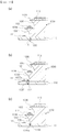
FIG. 1 is a perspective view showing an LED illumination device in the related art. In the LED illumination device, a plurality ofLED devices 11 is disposed on asubstrate 12, which is disposed on aheat sink 13 such that the heat that is generated when theLED devices 11 emit light can be dissipated to the outside. Heat dissipation fins 14 protrude from the outer surface of theheat sink 13 so as to increase the area of heat dissipation. Asocket 15 is connected to an external power source, and atransparent cover 16 protects theLED devices 11 from the external environment. - However, since the
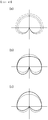
LED device 11 defines an angular range of radiation from 120° to 130° when emitting light, an LED illumination device, which is realized using theLED devices 11, exhibits a light distribution, as shown inFIG. 9B , which is focused substantially in the forward direction but not in the backward direction. - Accordingly, when the LED illumination device radiates light, it cannot realize light distribution the same as that of an incandescent lamp, that is, light distribution in which light is directed backward, as shown in
FIG. 9A . This causes a problem in that a sufficient intensity of illumination cannot be ensured in indoor or outdoor spaces. - Illumination devices according to the state of the art are known from documents
JP 2003 258319 A WO 2010/038982 A2 ,US 2009/021931 A1 ,EP 2 123 973 A2 ,EP 1 582 405 A2DE 10 2004 025473 A1 . - Exemplary embodiments of the present disclosure provide a Light Emitting Diode (LED) illumination device.
- Exemplary embodiments of the present disclosure also provide an LED illumination device that can achieve a wide light distribution with an increased angular range of radiation by directing a portion of the light that is generated by the light source to the side and rear of the illumination device.
- Exemplary embodiments of the present disclosure also provide an LED illumination device that has an increased angular range of radiation and achieves uniform intensity of light by positioning a reflector, which directs a portion of the light that is generated from a light source to the side and rear of the illumination device, above and spaced apart from the light source.
- Exemplary embodiments of the present disclosure also provide an LED illumination device that can achieve uniform intensity of light by arranging a plurality of light sources in peripheral and inner areas of a substrate such that the light sources do not overlap each other.
- Exemplary embodiments of the present disclosure also provide an LED illumination device that achieves uniform intensity of light by designing a reflector, which reflects light that is generated from a plurality of light sources, in a multistory structure such that the light sources are arranged at different heights.
- Exemplary embodiments of the present disclosure also provide an LED illumination device that achieves a variety of light distribution patterns by radiating light that is generated by a first light source and light that is generated by a second light source to the outside through respective first and second covers, which are partitioned by a reflector and have different transmittances.
- Exemplary embodiments of the present disclosure also provide an LED illumination device that can be easily implemented since a fluorescent material, which converts light that is generated by an LED into white light, is contained in a cover.
- Exemplary embodiments of the present disclosure also provide an LED illumination device that achieves a variety of illumination patterns according to the mood by separating light that is generated by a first light source and light that is generated by a second light source from each other using a reflector, the first and second light sources being designed to generate different types of light.
- Exemplary embodiments of the present disclosure also provide an LED illumination device that guides light that is generated by a light source to the rear and reduces the interference of the light using a cover, which is provided above a heat sink on which a substrate is mounted, thereby minimizing the loss of the light that is radiated to the rear is minimized.
- Exemplary embodiments of the present disclosure also provide an LED illumination device that decreases the distance between a light source and a cover, which surrounds the light source, by forming the cover to be aspheric, so that the loss of the light that is radiated to the front is minimized, thereby increasing the entire light efficiency.
- The invention is defined by the subject-matter of the appended claims. An exemplary embodiment of the present disclosure discloses an LED illumination device that includes a substrate, at least one first light source disposed on a peripheral area of the substrate, at least one second light source disposed on an inner area of the substrate, and at least one reflector disposed on a boundary area between the first light source and the second light source. The reflector reflects light that is generated by the first light source to a side and a rear.
- An exemplary embodiment of the present disclosure also discloses an LED illumination device that includes a substrate, a plurality of first light sources disposed on a peripheral area of the substrate, at least one reflector disposed in an inner area of the substrate, the reflector having a predetermined height to reflect light that is generated by the first light sources to a side and a rear, and a plurality of second light sources disposed on an upper surface of the reflector such that the second light sources differ in height from the first light sources. The second light sources are electrically connected to the substrate. The second light sources alternate with the first light sources that are disposed adjacent to the second light sources.
- An exemplary embodiment of the present disclosure also discloses an LED illumination device that includes a substrate; a light source including at least one first light source disposed on a peripheral area of the substrate and at least one second light source disposed on an inner area of the substrate; a reflector disposed on a boundary area between the first light source and the second light source and having a predetermined height, the reflector separating light that is generated by the first light source from light that is generated by the second light source; and a cover including a first cover allowing the light that is generated by the first light source to pass to an outside and a second cover allowing the light that is generated by the second light source to pass to an outside. The first and second covers have different transmittances.
- An exemplary embodiment of the present disclosure also discloses an LED illumination device that includes a substrate; a light source including at least one first light source and at least one second light source, which are disposed on the substrate; a reflector for reflecting light that is generated by the first light source and the second light source, the reflector being disposed such that it partitions an area of the first light source from an area of the second light source; a cover for allowing the light that is generated by the light source to pass through; a heat sink disposed on an underside of the substrate; and an inclined guide surface formed on the heat sink, wherein the incline of the guide surface increases from an edge of an upper surface toward a lower portion of the heat sink. The guide surface has a maximum outer diameter that is equal to or smaller than that of the cover.
- According to embodiments of the disclosure, the reflector is disposed in the boundary area between the first light source, which is disposed on the substrate, and the second light source, which is disposed on the substrate in an area that is more inward than that of the first light source, in order to reflect light that is generated by the first light source toward the side and rear, thereby increasing the angular range of radiation. Consequently, the distribution of light that is generated by the first light source can be made similar to that of an incandescent lamp. Accordingly, the LED illumination device can replace the incandescent lamp in lighting devices that use incandescent lamps without decreasing illumination efficiency. In addition, since a wide angular range can be achieved, the LED illumination device can be used for main illumination rather than localized illumination, thereby increasing the range of use and applicability.
- In addition, it is possible to increase the angular range and achieve uniform intensity of light by positioning a reflector, which directs a portion of the light that is generated by the light source toward the side and rear of the illumination device, above and spaced apart from the light source, which is disposed on a substrate.
- Furthermore, it is possible to achieve uniform intensity of light by arranging a plurality of light sources, which are disposed on the peripheral and inner areas of a substrate, such that they do not overlap each other.
- In addition, it is possible to achieve uniform intensity of light by arranging a plurality of light sources, which are disposed on the peripheral and inner areas of the substrate, such that they do not overlap each other and are positioned at different heights.
- In addition, it is possible to achieve a variety of light distribution patterns by radiating light that is generated by the first light source and light that is generated by the second light source to the outside through the respective first and second covers, which are partitioned by the reflector and have different transmittances.
- Furthermore, it is possible to easily fabricate the LED illumination device and improve productivity, since the fluorescent material, which converts light that is generated by the LED into white light, is contained in the cover.
- In addition, it is possible to achieve a variety of illumination patterns according to the mood by separating light that is generated by the first light source and light that is generated by the second light source from each other using the reflector, the first and second light sources being designed to generate different types of light.
- Furthermore, it is possible to guide light that is generated by the light source to the rear and reduce the interference of the light using the cover, which is provided above the heat sink on which the substrate is mounted, so that the loss of the light that is radiated to the rear is minimized, thereby increasing the entire light efficiency.
- Moreover, it is possible to decrease the distance between the light source and the cover, which surrounds the light source, by forming the cover to be aspheric, so that the loss of the light that is radiated to the front is minimized, thereby increasing the entire light efficiency.
- It is to be understood that both the foregoing general description and the following detailed description are exemplary and explanatory and are intended to provide further explanation of the invention as claimed.
-
-
FIG. 1 is a perspective view showing an LED illumination device in the related art. -
FIG. 2 is a cross-sectional view showing the overall configuration of an LED illumination device according to a first exemplary embodiment of the disclosure. -
FIG. 3 is a perspective view showing the LED illumination device according to the first exemplary embodiment of the disclosure. -
FIG. 4 is a top plan view showing the layout of the light sources shown inFIG. 3 . -
FIG. 5 is a detailed view showing the reflection of light by the reflector and the travel of light in the case in which the reflector employed in the present invention is disposed on the upper surface of the substrate. -
FIG. 6A, FIG. 6B, FIG. 6C, and FIG. 6D are cross-sectional views showing several structures of the reflector employed in the present disclosure, in whichFIG. 6A is a single curved structure,FIG. 6B is a combination of a straight vertical section and an inclined section,FIG. 6C is a combination of a curved section and an inclined section, andFIG. 6D is a combination of a straight vertical section and a curved section. -
FIG. 7A, FIG. 7B, and FIG. 7C are cross-sectional views showing several coupling states between the reflector and the substrate, which are employed in the present disclosure, in whichFIG. 7A is a fitting type using a fitting protrusion,FIG. 7B is a faster type using a fastening member, andFIG. 7C is a bonding type using an adhesive. -
FIG. 8A, FIG. 8B, and FIG. 8C are top plan views showing several structures of the reflector employed in the present disclosure, in whichFIG. 8A shows a reflector having a cavity,FIG. 8B shows a reflector having a wavy cross section, andFIG. 8C shows a reflector having a toothed cross section. -
FIG. 9A, FIG. 9B, and FIG. 9C are graphs showing the distribution of light that is generated from a light source, in which an incandescent lamp was used inFIG. 9A , an LED illumination device of the related art was used inFIG. 9A , and an LED illumination device of the present disclosure was used inFIG. 9A . -
FIG. 10 is a cross-sectional view showing the overall configuration of an LED illumination device according to a second exemplary embodiment of the disclosure. -
FIG. 11 is a perspective view of the LED illumination device shown inFIG. 10 . -
FIG. 12 is a cross-sectional view showing the overall configuration of an LED illumination device according to a third exemplary embodiment of the disclosure. -
FIG. 13 is a perspective view of the LED illumination device shown inFIG. 12 . -
FIG. 14 is a cross-sectional view showing the overall configuration of an LED illumination device according to a fourth exemplary embodiment of the disclosure. -
FIG. 15 is a perspective view of the LED illumination device shown inFIG. 14 . -
FIG. 16 is a cross-sectional view showing the overall configuration of an LED illumination device according to a fifth exemplary embodiment of the disclosure. -
FIG. 17 is a perspective view of the LED illumination device shown inFIG. 16 . -
FIG. 18 is a cross-sectional view showing the overall configuration of an LED illumination device according to a sixth exemplary embodiment of the disclosure. -
FIG. 19 is a perspective view of the LED illumination device shown inFIG. 18 . -
FIG. 20 is a detailed view showing the reflection of light by the reflector and the travel of light in the LED illumination device shown inFIG. 18 . -
FIG. 21 is a cross-sectional view showing the overall configuration of an LED illumination device according to a seventh exemplary embodiment of the disclosure. -
FIG. 22 is a perspective view of the LED illumination device shown inFIG. 21 . -
FIG. 23 is a detailed view showing the reflection of light by the reflector and the travel of light in the LED illumination device shown inFIG. 21 . -
FIG. 24 is a cross-sectional view showing the overall configuration of an LED illumination device according to an eighth exemplary embodiment of the disclosure. -
FIG. 25 is a perspective view of the LED illumination device shown inFIG. 24 . -
FIG. 26 is a detailed view showing the reflection of light by the reflector and the travel of light in the LED illumination device shown inFIG. 24 . -
FIG. 27 is a cross-sectional view showing the overall configuration of an LED illumination device according to a ninth exemplary embodiment of the disclosure. -
FIG. 28 is a perspective view of the LED illumination device shown inFIG. 27 . -
FIG. 29 is a detailed view showing the reflection of light by the reflector and the travel of light in the LED illumination device shown inFIG. 27 . -
FIG. 30 is a cross-sectional view showing the overall configuration of an LED illumination device according to a tenth exemplary embodiment of the disclosure. -
FIG. 31 is a perspective view showing the LED illumination device according to the tenth exemplary embodiment of the disclosure. -
FIG. 32 is a top plan view showing the arrangement of light sources in the LED illumination device according to the tenth exemplary embodiment of the disclosure. -
FIG. 33 is a detailed view showing the reflection of light by the reflector and the travel of light in the case in which the reflector is disposed on the top surface of the substrate in the LED illumination device shown inFIG. 30 . -
FIG. 34A, FIG. 34B, FIG. 34C, FIG. 34D, and FIG. 34E are cross-sectional views showing several structures of the reflector employed in the tenth exemplary embodiment of the present disclosure, in whichFIG. 34A is a single straight structure,FIG. 34B is a single curved structure,FIG. 34C is a combination of a straight vertical section and an inclined section,FIG. 34D is a combination of a curved section and an inclined section, andFIG. 34E is a combination of a straight vertical section and a curved section. -
FIG. 35A, FIG. 35B, and FIG. 35C are cross-sectional views showing several structures in which the reflector is coupled to the substrate in the LED illumination device shown inFIG. 30 , in whichFIG. 35A shows a fitting type using a hook,FIG. 35B shows a fastening type using a fastening member, andFIG. 35C shows a bonding type using an adhesive. -
FIG. 36A, FIG. 36B, and FIG. 36C are top plan views showing several structures of the second surface of the reflector in the LED illumination device shown inFIG. 30 , in whichFIG. 36A shows a reflector having a circular cross section,FIG. 36B shows a reflector having a wavy cross section, andFIG. 36C shows a reflector having a toothed cross section. -
FIG. 37 is a cross-sectional view showing the overall configuration of an LED illumination device according to an eleventh embodiment of the present disclosure. -
FIG. 38 is a perspective view of the LED illumination device shown inFIG. 37 . -
FIG. 39 is a detailed view showing the reflection of light by the reflector and the travel of light in the LED illumination device shown inFIG 37 . -
FIG. 40 is a configuration view of the LED illumination device shown inFIG. 37 , which contains the fluorescent material in the cover. -
FIG. 41 is a view showing a variation of the LED illumination device shown inFIG. 37 . -
FIG. 42 is a configuration view showing an LED illumination device according to the eleventh embodiment of the present disclosure, in which a first light source and a second light source are implemented as LEDs having different colors; -
FIG. 43A, FIG. 43B, and FIG. 43C are graphs showing light distribution depending on the transmittances of the first and second covers in the LED illumination device according to the eleventh embodiment of the present disclosure, in whichFIG. 43A shows the case in which the first and second covers have the same transmittance,FIG. 43B shows the case in which the transmittance of the first cover is higher than that of the second cover, andFIG. 43C shows the case in which the transmittance of the second cover is lower than that of the first cover; -
FIG. 44 is a cross-sectional view showing the overall of an LED illumination device according to a twelfth embodiment of the present disclosure; -
FIG. 45 is a perspective view of the LED illumination device shown inFIG. 44 ; -
FIG. 46 is a detailed view showing the reflection of light by the reflector and the travel of light in the LED illumination device shown inFIG. 44 ; -
FIG. 47 is a configuration view of the LED illumination device shown inFIG. 44 , which contains the fluorescent material in the cover; -
FIG. 48 is a view showing a variation of the LED illumination device shown inFIG. 46 ; -
FIG. 49 is a view showing another coupling relationship between the cover and the heat sink in the LED illumination device shown inFIG. 46 ; and -
FIG. 50 is an overall configuration view of the LED illumination device shown inFIG. 46 , which has the cover coupled to the mounting surface of the heat sink. - The invention is described more fully hereinafter with reference to the accompanying drawings, in some of which embodiments of the invention are shown. This invention may, however, be embodied in many different forms and should not be construed as limited to the exemplary embodiments set forth herein, provided they fall within the scope of the appended claims. Rather, these exemplary embodiments are provided so that this disclosure is thorough, and will fully convey the scope of the invention to those skilled in the art. In the drawings, the size and relative sizes of layers and regions may be exaggerated for clarity. Like reference numerals in the drawings denote like elements.
- It will be understood that when an element or layer is referred to as being "on" or "connected to" another element or layer, it can be directly on or directly connected to the other element or layer, or intervening elements or layers may be present. In contrast, when an element is referred to as being "directly on" or "directly connected to" another element or layer, there are no intervening elements or layers present.
- Throughout this document, reference should be made to the drawings, in which the same reference numerals and signs are used throughout the different drawings to designate the same or similar components.
- Light emitting diode (LED)
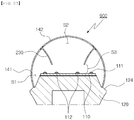
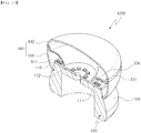
illumination devices substrate 110, a firstlight source 111, a secondlight source 112, and areflector FIG. 2 to FIG. 50 . - The
substrate 110 is a circuit board member, which has a predetermined circuit pattern formed on the upper surface thereof, such that the circuit pattern is electrically connected to external power, which is supplied through a power cable (not shown), and is electrically connected to the light sources. - The
substrate 110 is disposed on the upper surface of aheat sink 120, with aheat dissipation pad 121 interposed between thesubstrate 110 and theheat sink 120. It is preferred that theheat sink 120 be made of a metal, such as aluminum (Al), having excellent heat conductivity, such that it can dissipate the heat that is generated when the light sources emit light to the outside. - The
heat sink 120 may have a plurality of heat dissipation fins on the outer surface thereof in order to increase heat dissipation efficiency by increasing the heat dissipation area. Theheat sink 120 may have aguide surface 124 on the upper portion thereof, theguide surface 124 being cut open from the inside to the outside. In the process in which a portion of the light that is generated by the light sources is reflected to the side and rear by thereflector guide surface 124 increases the area through which the light can travel in the rearward direction, thereby increasing the angular range of radiation of the light. In this fashion, theguide surface 124 can guide the light that is reflected from thereflector - Although the
substrate 110 has been shown and described as having the form of a disc conforming to the shape of the mounting area, i.e. the upper surface of theheat sink 120, this is not intended to be limiting. Rather, thesubstrate 110 may be formed as a polygonal plate, such as a triangular or rectangular plate. - In addition, although the
substrate 110 has been shown and described as being bonded to the upper surface of the heat sink via theheat dissipation pad 121, this is not intended to be limiting. It should be understood that thesubstrate 110 may be detachably assembled to the mountingarea 122 of theheat sink 120 via a fastening member. - In addition, a light-transmitting
cover 140 having a space S therein is provided on the outer circumference of the mounting area of theheat sink 120. The light-transmittingcover 140 radiates the light that is emitted from the light sources to the outside while protecting the light sources. It is preferred that the light-transmittingcover 140 be formed as a light diffuser cover in order to radiate the light that is generated by the light sources to the outside by diffusing it. - Although the light-transmitting
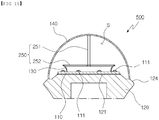
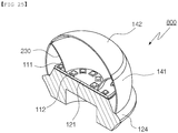
cover 140 has been shown and described as being hemispherical, this is not intended to be limiting. Rather, the light-transmittingcover 140 may have anextension 231, which extends from a middle portion in the height direction to the lower portion of the hemisphere, in order to increase the reflection area, in which light is reflected to the side and rear by thereflector FIG. 26 ). Theextension 231 is bent inward at a predetermined angle such that it is positioned lower than the height at which the firstlight source 111 is disposed on thesubstrate 110, thereby increasing the area that is illuminated by the light emitted from the firstlight source 111. - The
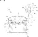
reflector substrate 110, as shown inFIG. 2 to FIG. 50 , and serves to reflect the light that is generated by the firstlight source 111 to the side and rear. - The
reflector light sources 121, which are disposed on the peripheral area of thesubstrate 110, and the one or more secondlight sources 112, which are disposed on the inner area of thesubstrate 110. Thereflector light source 111, which is arranged on the peripheral area, to the side and rear with respect to thesubstrate 110. - Here, the first
light source 111 and the secondlight source 112 may be formed as a chip-on-board (COB) assembly, in which a plurality of LED chips is integrated on aboard 114, as shown inFIG. 10 , an LED package including lead frames, or a combination thereof. - As shown in
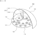
FIG. 2 andFIG. 3 , the firstlight source 111, which includes a plurality of LED devices, is arrayed in a predetermined pattern on the peripheral area of thesubstrate 110, and the secondlight source 112, which includes a plurality of LED devices, is arrayed in a predetermined pattern on the inner area of thesubstrate 110. - In the case in which the first
light source 111 includes a plurality of first LED devices and the secondlight source 112 includes a plurality of second LED devices, it is preferred that thesecond LED devices 112 be positioned such that they alternate with thefirst LED devices 111, which are disposed on the peripheral area of thesubstrate 110, as shown inFIG. 4 . This is intended to make the light that is generated by thefirst LED devices 111 and the light that is generated by thesecond LED devices 112 to share the entire area of the light-transmittingcover 140, so that overall intensity of light is uniform. - In addition, as shown in
FIG. 10 andFIG. 11 , the secondlight source 112 in the inner area may be provided as a COB assembly, in which the LED chips are integrated. The firstlight source 111 in the peripheral area may include the packaged LED devices. - As shown in
FIG. 12 to FIG. 15 , both the firstlight source 111, which is disposed in the peripheral area of thesubstrate 110, and the secondlight source 112, which is disposed in the inner area, may be provided as a COB assembly. - Here, if both the first
light source 111 and the secondlight source 112 are formed as a COB assembly, the firstlight source 111 and the secondlight source 112 may be disposed on oneboard 114, such that the firstlight source 111, the secondlight source 112, and thereflector 130 may form a single device. In this case, the lower end of thereflector 130 is fixed to the upper surface of theboard 114. - In addition, as shown in
FIG. 14 andFIG. 15 , theboard 114 on which theLED chips 112 are disposed is divided into two sections, including afirst board 114a, which is disposed on the peripheral area of thesubstrate 110, and asecond board 114b, which is disposed in the inner area of thesubstrate 110. The LED chips 111 that act as the first light source may be integrally disposed on thefirst board 114a, and theLED chips 112 that act as the second light source may be integrally disposed on thesecond board 114b. In this case, thereflector 130 is disposed at the boundary between thefirst board 114a and thesecond board 114b, and the lower end of thereflector 130 is fixed to thesubstrate 110, which is disposed under the first and second boards 123a and 123b. - In the case in which the lower end of the reflector is fixed to the
substrate 110 or theboard 114 as described above, a portion of light L1 that is generated by the firstlight source 111, which is disposed on the peripheral area of thesubstrate 110 or theboard 114, is reflected by the outer surface of thereflector 130 so that it is radiated to the side and rear with respect to thesubstrate 110 as shown inFIG. 5 . At the same time, the remaining portion of the light L1 is not reflected by thereflector cover 140. - In addition, light L2 that is generated by the second
light source 112, which is disposed on the inner area of thesubstrate 110, is radiated toward the light-transmittingcover 140, either by being reflected by the inner surface of thereflector 130 or without being reflected by thereflector - Here, the shape of the
heat sink 120 must be optimally designed in order to minimize interference of the portion of the light L1 that is generated by the firstlight source 111. Otherwise, the portion of the light L1 encounters interference by striking theheat sink 120 while traveling backward by being reflected by the outer surface of thereflector guide surface 124, which has a downward incline at a predetermined angle, may be provided on the outer circumference of theheat sink 120 on which thesubstrate 110 is disposed. - The
reflectors light source 111 to be radiated directly to the front with respect to thesubstrate 110 while the remaining portion of the light L1 is reflected to the side and rear. - As shown in
FIG. 6A , thereflector 130a may be configured as a curved reflector plate, in which the lower end thereof is fixed to thesubstrate 110, and the upper end thereof is oriented toward the firstlight source 111. - In addition, as shown in
FIG. 6B , thereflector 130b may be configured as a reflector plate that has avertical section 131 and aninclined section 132. Thevertical section 131 vertically extends a predetermined height from the lower end thereof, which is fixed to thesubstrate 110. Theinclined section 132 extends at an incline at a predetermined angle from the upper end of thevertical section 131 toward the firstlight source 111. - Furthermore, as shown in
FIG. 6C , thereflector 130c may be configured as a reflector plate that has a lowercurved section 133 and aninclined section 132. The lowercurved section 133 is curved from the lower end thereof, which is fixed to thesubstrate 110, toward the firstlight source 111. Theinclined section 132 extends at an incline at a predetermined angle from the upper end of the lowercurved section 133 toward the firstlight source 111. - In addition, as shown in
FIG. 6D , thereflector 130d may be configured as a reflector plate that has avertical section 131 and an uppercurved section 134. Thevertical section 131 vertically extends a predetermined height from the lower end thereof, which is fixed to thesubstrate 110. The uppercurved section 134 is curved from the upper end of thevertical section 131 toward the firstlight source 111. - The
vertical section 131 and theinclined section 132 are connected to each other at a joint C1, the lowercurved section 133 and theinclined section 132 are connected to each other at a joint C2, and thevertical section 131 and the uppercurved section 134 are connected to each other at a joint C3. It is preferred that the joints C1, C2, and C3 be positioned at the same height as or higher than the firstlight source 111 so that the light L1 that is generated by the firstlight source 111 can be reflected to the side or rear. - Although the joints C1, C2, and C3 have been described as being integral with
respective reflectors respective reflectors - In each of the
reflectors light source 111, such that a portion of the light L1 that is generated by the firstlight source 111 is radiated to the side and rear by being reflected by the reflector and the remaining portion of the light L1 is radiated to the front together with the light L2 that is generated by the secondlight source 112. - In addition, the
reflectors layers 135 may be provided on the outer surface of thereflectors - The reflecting
layer 135 may be formed on the surface of the reflector to a predetermined thickness. For this, a reflective material, such as aluminum (Al) or chromium (Cr), may be applied to the surface of the reflector by a variety of methods, such as deposition, anodizing, or plating. - Although the reflecting
layer 135 has been shown and described as being formed to a predetermined thickness on the entire outer surface of the reflector such that it can reflect all of the light that is generated by the first and secondlight sources layer 135 may be formed only on the outer surface of thereflectors light source 111, such that only the light L1 that is generated by the firstlight source 111 can be reflected. - In the case in which the
reflectors substrate 110 and the lower end of thereflectors - The
reflector 130 of this embodiment is provided as a reflector plate having a predetermined height, as shown inFIG. 2 to FIG. 8 andFIG. 10 to FIG. 16 . The lower end of the reflector may be fixedly assembled to thesubstrate 110 or theboard 114 by a variety of methods. An exemplary method is shown inFIG. 7 . - As shown in
FIG. 7A , thereflector 130 has ahook 136 on the lower end thereof. Thehook 136 is fitted into anassembly hole 116, which penetrates thesubstrate 110. In this position, thehook 136 generates a holding force, thereby preventing the lower end of thereflector 130 from becoming dislodged. - As shown in
FIG. 7B , thereflector 130 has acoupling section 137, which is bent from the lower end thereof to the side. Thecoupling section 137 may be fastened to acoupling hole 117, which penetrates thesubstrate 110, via afastening member 137a. - Although the
coupling section 137 has been shown as being bent toward the secondlight source 112 such that it can increase reflection efficiency by decreasing interference with the light that is generated by the firstlight source 111, this is not intended to be limiting. Rather, thecoupling section 137 may be bent toward the firstlight source 111. - In addition, as shown in
FIG. 7C , thereflector 130 has afitting protrusion 138 on the lower end thereof. Thefitting protrusion 138 is fitted into arecess 118, which is depressed into the upper surface of thesubstrate 110 to a predetermined depth, and is fixedly bonded thereto via an adhesive 138a. - Here, each of the
assembly hole 116, thecoupling hole 117, and therecess 118, which are formed in thesubstrate 110, must be configured such that it does not overlap a pattern circuit, which is printed on the upper surface of the substrate in order to supply electrical power to the firstlight source 111. Two ormore hooks 136 corresponding to the assembly holes 116 may be provided on the lower end of thereflector 130 such that they are spaced apart from each other at a predetermined interval. Two ormore coupling sections 137 corresponding to the coupling holes 117 and two or morefitting protrusions 138 corresponding to therecesses 118 may be provided on the lower end of thereflector 130 in the same manner. - In another embodiment of the
LED illumination device 500 of the present disclosure, as shown inFIG. 16 andFIG. 17 , thereflector 130 may be supported bysupport members 250, which connect thereflector 130 to the light-transmittingcover 140, with the lower end thereof being fixed to the upper surface of thesubstrate 110. - For this, the
support members 250 include avertical member 251, which has a predetermined height, andhorizontal members 252, which are connected to the lower end of thevertical member 251. Specifically, thevertical member 251 has a predetermined length, the upper end of thevertical member 251 is connected to the light-transmittingcover 140, and the lower end of thevertical member 251 is connected to thehorizontal members 252, which are disposed across thereflector 130. - The
horizontal members 252 are provided as a plurality of members, which extend in transverse directions from the center of thereflector 130. It is preferred that the point at which thehorizontal members 252 are connected to each other be connected to the lower end of thevertical member 251, and that thehorizontal members 252 be radially disposed in order to maintain the balance of force. - It is preferred that the sum of the vertical length of the
vertical member 251 and the height of thereflector 130 be the same as or greater than the maximum height from thesubstrate 110 to the light-transmittingcover 140, that the upper end of thevertical member 251 be connected to the center of the light-transmittingcover 140, and that the lower end of thevertical member 251 be disposed on the center of thereflector 130. - Consequently, when the light-transmitting
cover 140 and theheat sink 120 are coupled to each other, thehorizontal member 252 and thereflector 130 are pressed and supported downward by thevertical member 251 so that the lower end of thereflector 130 remains in contact with the upper surface of thesubstrate 110, thereby locating thereflector 130 in the boundary area between the firstlight source 111 and the secondlight source 112. - The
reflector 130, which is connected to the light-transmittingcover 140 by thesupport members 250, may be formed integrally with the light-transmittingcover 140, or may be configured such that the middle portion or the upper end of thevertical member 251 is detachably assembled to the light-transmittingcover 140. - In an example, the
vertical member 251 may be configured as two separate members, in which the adjoining ends of the two members are detachably assembled to each other via screw fastening or interference fitting. - As shown in
FIG. 18 to FIG. 23 , in further embodiments of theLED illumination devices reflector 130, which reflects light that is generated by the firstlight source 111 to the side or rear, may be spaced apart a predetermined height from thesubstrate 110. - For this,
support members 250 andspacer members 260 are provided such that the lower end of thereflector 130 is located in the boundary area between the firstlight source 111 and the secondlight source 112. - As described above, the
support members 250 may include onevertical member 251 and one or morehorizontal members 252. One end of thevertical member 251 is connected to the light-transmittingcover 140, and thehorizontal members 252 extend from the lower end of the vertical member 251 (seeFIG. 18 andFIG. 19 ). - Like the
support members 250 shown inFIG. 16 andFIG. 17 , thesupport members 250 are configured such that thevertical member 251 extends a predetermined height and thehorizontal members 252 are connected to the lower end of thevertical member 251. The upper end of thevertical member 251 is connected to the light-transmittingcover 140, and the lower end of thevertical member 251 is connected to thehorizontal members 252, which are disposed across thereflector 130. - The
horizontal members 252 are provided as a plurality of members, which extend in transverse directions from the center of thereflector 130. The point at which thehorizontal members 252 are connected to each other is connected to the lower end of thevertical member 251. It is preferred that thehorizontal members 252 be radially disposed in order to maintain the balance of force. - It is preferred that the sum of the vertical length of the
vertical member 251 and the height of thereflector 130 be smaller than the maximum height from thesubstrate 110 to the light-transmittingcover 140 such that the lower end of thereflector 130 is spaced apart a predetermined length from thesubstrate 110, thereby defining a space S3 between the lower end of thereflector 130 and the upper surface of thesubstrate 110. - Consequently, when the light-transmitting
cover 140 is coupled to theheat sink 120, thehorizontal members 252 and thereflector 130 are disposed in the space S in the light-transmittingcover 140 in the state in which they are spaced apart a predetermined height from the upper surface of thesubstrate 110 by thevertical member 251. - The
reflector 130, which is connected to the light-transmittingcover 140 by thesupport members 250, may be formed integrally with the light-transmittingcover 140, or may be configured such that the middle portion or the upper end of thevertical member 251 is detachably assembled to the light-transmittingcover 140. - In an example, the
vertical member 251 may be configured as two separate members, in which the adjoining ends of the two members may be detachably assembled to each other via screw fastening or interference fitting. - Another configuration, in which the
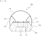
reflector 130 is spaced apart a predetermined height from thesubstrate 110 to define a space S3 between the lower end of thereflector 130 and the upper surface of thesubstrate 110, is shown inFIG. 21 andFIG. 22 . - Here, provided are one or
more spacer members 260 having a predetermined height, which connect the lower end of thereflector 130 to the upper end of thesubstrate 110, such that thereflector 130 is spaced apart a predetermined height from thesubstrate 110. For structural stability, it is preferred that thespacer members 260 be two or more members, which are radially disposed. - The upper end of the
spacer member 260 is connected to the lower end of thereflector 130 and the lower end of thespacer member 260 is fixed to the upper surface of thesubstrate 110. It should be appreciated that the lower end of thespacer member 260 may be fixed to thesubstrate 110 by a plurality of structures, as shown inFIG. 7 . - In the case in which the
reflector 130 is spaced apart a predetermined height from thesubstrate 110 via thesupport members 250 or thespacer members 260, the state in which light is reflected by thereflector 130 is shown inFIG. 20 andFIG. 23 . - As shown in
FIG. 20 andFIG. 23 , a portion of the light that is generated by the firstlight source 111 is radiated to the side and rear with respect to thesubstrate 110 by being reflected by the outer surface of thereflector 130, and the remaining portion of the light L1 is radiated toward the area above the secondlight source 112 by being reflected from the inner surface of thereflector 130, or is directly radiated toward the area above the secondlight source 112. Consequently, the light that is generated by the firstlight source 111 is radiated on all of the center, side, and rear of the light-transmittingcover 140 without being reflected to the side and rear of the reflector. In this manner, the light can be uniformly radiated, rather than being concentrated in a specific area. - The
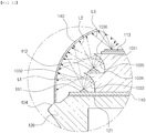
LED illumination devices FIG. 25 to FIG. 29 , the light-transmittingcover 140 includes two sections, i.e. afirst cover 141 and asecond cover 142. The first andsecond covers reflector 230. - The lower end of the
reflector 230 is disposed on the boundary area between the firstlight source 111 and the secondlight source 112, and the upper end of thereflector 230 is fixedly connected to the light-transmittingcover 140. For this, theextension 231 of thereflector 230 diverges and extends a predetermined length toward thefirst cover 141 and toward thesecond cover 142. - The
extension 231 is in contact with and meshed with one end of thefirst cover 141 and one end of thesecond cover 142, and serves to couple the first andsecond cover portion 232, which is depressed to a predetermined depth, is formed in one end of thefirst cover 141, which is coupled with theextension 231. The other steppedportion 232, having the same configuration, is formed in one end of thesecond cover 142, which is coupled with theextension 231. - It should be understood that the
extension 231 may be fixed by a variety of structures, including a structure in which theextension 231 is fixed to the stepped portions of thefirst cover 141 and thesecond cover 142 via an adhesive, and a structure in which theextension 231 is fitted into the recesses that are respectively formed in one end of thefirst cover 141 and in one end ofsecond cover 142. - In the
reflector 230 having the upper end connected to the light-transmittingcover 140, the lower end of thereflector 230 is in contact with the upper surface of thesubstrate 110. More particularly, the lower end of thereflector 230 is in contact with the boundary area between the firstlight source 111 and the secondlight source 112, or is spaced apart a predetermined height from thesubstrate 110 while being disposed in the boundary area between the first and secondlight sources - In the case in which the lower end of the
reflector 230 is in contact with the substrate, as shown inFIG. 24 andFIG. 25 , the space S inside the light-transmittingcover 140 is divided into two sections by thereflector 230. Consequently, the light L1 that is generated by the firstlight source 111 is radiated to the side and rear with respect to thesubstrate 110 by being reflected by the outer surface of thereflector 230, whereas the light L2 that is generated by the secondlight source 112 is radiated toward thesecond cover 142 by being reflected by the inner surface of thereflector 230, or is directly radiated toward the second cover 142 (seeFIG. 26 ) . - In addition, as shown in
FIG. 27 andFIG. 28 , in the case in which the lower end of thereflector 230 is located in the boundary area between the firstlight source 111 and the secondlight source 112 and is spaced apart a predetermined height from thesubstrate 110, the space S of the light-transmittingcover 140 is divided into the spaces S1, S2, and S3. In the space S1, the light that is generated by the firstlight source 111 is reflected to the side and rear by the outer surface of thereflector 230. In the space S2, the light is reflected by the inner surface of thereflector 230, or is directly radiated toward thesecond cover 142. In addition, the light that is generated by the firstlight source 111 is radiated toward thesecond cover 142 by passing through the space S3. The light that is generated by the firstlight source 111 and the secondlight source 112 is radiated along paths shown inFIG. 29 toward thefirst cover 141 and thesecond cover 142. - In this embodiment, the lower end of the
reflector 230 is spaced a predetermined height from thesubstrate 110 for the same reason as described in the foregoing embodiments. Specifically, the light that is generated by the firstlight source 111 is also radiated toward thesecond cover 142 through the space S3 instead of being entirely reflected to the side and rear by the reflector. In this manner, the light can be uniformly radiated, rather than being concentrated in a specific area. - The
reflectors FIG. 8 . - Specifically, as shown in
FIG. 8A , thereflectors light source 111 and the secondlight source 112. - As shown in
FIG. 8B , thereflector 130e may be configured as a reflector plate that has a wavy cross-sectional shape. Specifically, waves continue for a predetermined period such that the light that is generated by the firstlight source 111 or the secondlight source 112 can be diffused again in the direction parallel to thesubstrate 110. - In addition, as shown in
FIG. 8C , thereflector 130f may be configured as a reflector plate that has a toothed cross-sectional shape, in which teeth continue for a predetermined period such that the light that is generated by the firstlight source 111 or the secondlight source 112 can be diffused again in the direction parallel to thesubstrate 110. - In the
LED illumination devices reflectors light source 111 and the secondlight source 112. When the firstlight source 111 and the secondlight source 112 are turned on when external power is applied thereto, a portion of the light L1 that is generated by the firstlight source 111 is reflected by the outer surface of the reflector, the cross section of which is curved or inclined toward the firstlight source 111, so that the portion of the light L1 travels to the side or rear, whereas the remaining portion of the light L1 travels toward the light-transmittingcover 140 without being reflected by the reflector. - In addition, the light L2 that is generated by the second
light source 112 travels toward the light-transmittingcover 140 by being reflected by the inner surface of the reflector or without being interfered by the reflector. Consequently, theLED illumination devices FIG. 9C ) the same as light distribution (seeFIG. 9B ) that can be produced from an incandescent lamp, and produce an increased angular range of 270° or more. - Referring to
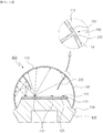
FIG. 30 to FIG. 36 , in theLED illumination device 1000 according to the tenth embodiment of the present disclosure, thereflector 1030 has an inclined surface, which reflects light that is generated by a light source, and a horizontal surface on which the light source is disposed. - Here, the
LED illumination device 1000 includes thesubstrate 110, the firstlight source 111, the secondlight source 112, and thereflector 1030. - In the
reflector 1030 having the horizontal surface and the inclined surface, descriptions of the substrate on which thereflector 130 is disposed, the heat sink, and the light-transmitting cover are omitted since they are the same as those described above. In addition, the same reference numerals and signs are used to designate the substrate, the heat sink, and the light-transmitting cover. - The
reflector 1030 shown inFIG. 30 to FIG. 36 is disposed on the upper portion of thesubstrate 110, and serves to reflect the light that is generated by thelight sources - The
reflector 1030 is disposed in the inner area of thesubstrate 110 with a predetermined height, and the secondlight source 112 is disposed on the upper surface of thereflector 1030. Consequently, a plurality of firstlight sources 111 is disposed in the boundary area of thesubstrate 110, outside of thereflector 1030, and a plurality of secondlight sources 112 is disposed on the upper surface of thereflector 1030. Asecond surface 1033, which forms the side surface of thereflector 1030, is inclined at a predetermined angle to the firstlight source 111 such that the light that is generated by the firstlight source 111 can be reflected to the side and rear with respect to thesubstrate 110. - Here, it is preferred that the second
light sources 112, which are disposed on the upper surface of thereflector 1030, be disposed between respective firstlight sources 111, which are disposed along the periphery of thesubstrate 110, as shown inFIG. 32 . This is intended to make the light that is generated by thefirst light sources 111 and the light that is generated by the secondlight sources 112 to share the entire area of the light-transmittingcover 140, so that overall intensity of light is uniform. - It is preferred that the
reflector 1030 have a multistory structure, which is bent inward. Specifically, afirst surface 1034 is formed in the middle of the height of thereflector 1030, such that the light source is disposed on thefirst surface 1034, and asecond surface 1035 reflects the light that is generated by the light source disposed on the first surface to the side and rear. This is intended to increase the uniformity of the overall intensity of light by disposing the light sources on thefirst surface 1034, which has different heights, such that the light that is generated by the light sources can be reflected by thesecond surface 1035. - In the case in which the
reflector 1030 has the multistory structure, anupper story 1031 and alower story 1032 are arranged concentrically, with the cross-sectional area of the upper story being smaller than that of the lower story. This is intended to allow a portion of the light L2 that is generated by the light source, which is disposed on thefirst surface 1034, to be reflected by thesecond surface 1035, which forms the side surface of the upper story, to the side and rear, whereas the remaining portion of the light L2 is directly radiated toward the light-transmittingcover 140 without being reflected by thereflector 1030. - Although the
reflector 1030 has been shown as having the two-story structure, this is not intended to be limiting. Rather, it should be understood that the reflector may have three or more stories in which thefirst surface 1034 and thesecond surfaces first surface 1034 has been shown as a horizontal surface, this is not intended to be limiting. Rather, it should be understood that thefirst surface 1034 may be an inclined surface that has a downward incline at a predetermined angle. - For the sake of explanation, a description is given below of a two-story structure of the
reflector 1030. In thereflector 1030, afirst story 1032 has thefirst surface 1034 and thesecond surface 1033, and asecond story 1031 has thesecond surface 1035 and anupper surface 1036. - In this embodiment, the first
light source 111 is disposed in the boundary area of thesubstrate 110, the secondlight source 112 is disposed on thefirst surface 1034 of thefirst story 1032, and a thirdlight source 113 is disposed on theupper surface 1036 of thesecond story 1031. The first, second, and thirdlight sources substrate 110. Thesecond surface 1033, which forms the side surface of thefirst story 1032, and thesecond surface 1035, which forms the side surface of thesecond story 1031, have the same cross-sectional shape, and are inclined at the same predetermined angle toward the firstlight source 111 and the secondlight source 112. - Consequently, the
second surface 1033, which forms the side surface of thefirst story 1032, reflects a portion of the light that is generated by the firstlight source 111 to the side and rear, and thesecond surface 1035, which forms the side surface of thesecond story 1031, reflects a portion of the light that is generated by the secondlight source 112 to the side and rear. Light that is generated by the thirdlight source 113, which is disposed on theupper surface 1036 of thesecond story 1031, is directly radiated toward the light-transmittingcover 140 without being reflected by thereflector 1030. - In the
LED illumination device 1000 of this embodiment, the firstlight source 111, the secondlight source 112, and the thirdlight source 113 are located at different heights, such that the light L1 that is generated by the firstlight source 111 is radiated on the lower portion of the light-transmitting cover 140 (as designated with dotted lines inFIG. 33 ), the light L2 that is generated by the secondlight source 112 is radiated on the middle portion of the light-transmitting cover 140 (as designated with dashed dot linesFIG. 33 ), and the light L3 that is generated by the thirdlight source 113 is radiated on the central area of the light-transmitting cover 140 (as designated with solid lines inFIG. 33 ) . - Consequently, in the
LED illumination device 1000 of this embodiment, the light that is generated by the light sources is radiated to the side and rear with respect to thesubstrate 110 by being reflected by respectivesecond surfaces cover 140. This, as a result, can increase the uniformity of the intensity of light and realize light distribution similar to that of an incandescent lamp. - Here, the light sources may be formed as a chip-on-board (COB) assembly, in which a plurality of LED chips is integrated on a board, an LED package including lead frames, or a combination thereof. (See
FIG. 10 to FIG. 15 .) - In the
reflectors second surfaces light source 111 and the secondlight source 112 to be radiated directly to the front with respect to thesubstrate 110 while the remaining portion of the light L1 and L2 is reflected to the side and rear. - Specifically, as shown in
FIG. 34A , thereflector 1030a may have an overall conical shape. Specifically, thesecond surface 1033, which forms the side surface of thefirst story 1032, is a straight line that is inclined toward the firstlight source 111. Thesecond surface 1035, which forms the side surface of thesecond story 1031, is a straight line that is inclined toward the secondlight source 112. - In the
reflector 1030b shown inFIG. 34B , thesecond surface 1033 forms the side surface of thefirst story 1032, and is curved such that the upper end thereof is oriented toward the firstlight source 111. Thesecond surface 1035 forms the side surface of thesecond story 1031, and is curved such that the upper end thereof is oriented toward the secondlight source 112. - In the
reflector 1030c shown inFIG. 34C , thesecond surface 1033 forms the side surface of thefirst story 1032, and includes avertical section 1033a, which extends a predetermined height from the lower end thereof, and aninclined section 1033b, which extends at an incline at a predetermined angle from the upper end of thevertical section 1033a toward the firstlight source 111. In addition, thesecond surface 1035 forms the side surface of thesecond story 1031, and includes avertical section 1035a, which extends a predetermined height from the lower end thereof, and aninclined section 1035b, which extends at an incline at a predetermined angle from the upper end of thevertical section 1035a toward the secondlight source 112. - In the
reflector 1030d shown inFIG. 34D , thesecond surface 1033 forms the side surface of thefirst story 1032. Thesecond surface 1033 includes a lowercurved section 1033c, which is curved from the lower end thereof toward the firstlight source 111, and aninclined section 1033b, which extends at an incline at a predetermined angle from the upper end of the lowercurved section 1033c toward the firstlight source 111. In addition, thesecond surface 1035 forms the side surface of thesecond story 1031, and includes a lowercurved section 1035c, which is curved from the lower end thereof toward the secondlight source 112, and aninclined section 1035b, which extends at an incline at a predetermined angle from the upper end of the lowercurved section 1035c toward the secondlight source 112. - Furthermore, in the
reflector 1030e shown inFIG. 34E , thesecond surface 1033 forms the side surface of thefirst story 1032. Thesecond surface 1033 includes avertical section 1035a, which extends a predetermined height from the lower end thereof, and an uppercurved section 1033d, which is curved from the upper end of thevertical section 1033a toward the firstlight source 111. In addition, thesecond surface 1035 forms the side surface of thesecond story 1031, and includes avertical section 1035a, which extends a predetermined height from the lower end thereof, and an uppercurved section 1035d, which is curved from the upper end of thevertical section 1035a toward the secondlight source 112. - Here, it is preferred that a joint C1 in which the
inclined section 1033b is connected to thevertical section 1033a, a joint C2 in which theinclined section 1033a is connected to the lowercurved section 1033c, and a joint C3 in which the uppercurved section 1033d is connected to thevertical section 1033a be positioned at the same height as or higher than the firstlight source 111 so that the light L1 that is generated by the firstlight source 111 can be reflected to the side or rear. It is also preferred that a joint C1 in which theinclined section 1035b is connected to thevertical section 1035a, a joint C2 in which theinclined section 1035b is connected to the lowercurved section 1035c, and a joint C3 in which the uppercurved section 1035d is connected to thevertical section 1035a be positioned at the same height as or higher than the secondlight source 112 so that the light L2 that is generated by the first light source 1022 can be reflected to the side or rear. - Although the joints C1, C2, and C3 have been described as being integral with respective reflectors, this is not intended to be limiting. The joints C1, C2, and C3 may be assembled to the respective reflectors, depending on the design of the reflectors.
- In each of the
reflectors light source 111 and the free end of the second surface extends to the position directly above the secondlight source 112, such that a portion of the light L1 that is generated by the firstlight source 111 and a portion of the light L2 that is generated by the first light source 1022 are radiated to the side and rear by being reflected by the reflector while the remaining portions of the light L1 and L2 are radiated to the front. - The
reflectors layers 1070 may be formed on the outer surface of the reflector in order to increase reflection efficiency when reflecting the light that is generated by the light source. - The reflecting
layer 1070 may be formed on the surface of the reflector to a predetermined thickness. For this, a reflective material, such as aluminum (Al) or chromium (Cr), may be applied to the surface of the reflector by a variety of methods, such as deposition, anodizing, or plating. - In the case in which the
reflectors substrate 110 and the lower end of the reflector in order to prevent short circuits. - The
reflector 1030 of this embodiment has a multistory structure, as shown inFIG. 30 to FIG. 34 . The lower end of the reflector may be fixedly assembled to thesubstrate 110 by a variety of methods. An exemplary method is shown inFIG. 35 . - As shown in
FIG. 35A , thereflector 1030 has ahook 1039 on the lower end thereof. Thehook 136 is fitted into anassembly hole 116, which penetrates thesubstrate 110. In this position, thehook 1039 generates a holding force, thereby fixing the lower end of thereflector 1030 to the upper surface of thesubstrate 110. - As shown in
FIG. 35B , thereflector 1030 has acoupling section 1037, which is bent from the lower end thereof to the side. Thecoupling section 1037 may be fastened to acoupling hole 117, which penetrates thesubstrate 110, via afastening member 1037a. - In addition, as shown in
FIG. 35C , thereflector 1030 has afitting protrusion 1038 on the lower end thereof. Thefitting protrusion 1038 is fitted into arecess 118, which is depressed into the upper surface of thesubstrate 110 to a predetermined depth, and is fixedly bonded thereto via an adhesive 1038a. - Here, each of the
assembly hole 116, thecoupling hole 117, and therecess 118, which is formed in thesubstrate 110, must be configured such that it does not overlap a pattern circuit, which is printed on the upper surface of the substrate in order to supply electrical power to thelight sources more hooks 1039 corresponding to the assembly holes 116 may be provided on the lower end of thereflector 1030, such that they are spaced apart from each other at a predetermined interval. Two ormore coupling sections 1037 corresponding to the coupling holes 117 and two or morefitting protrusions 1038 corresponding to therecesses 118 may be provided on the lower end of thereflector 1030 in the same manner. - The
reflector 1030 of this embodiment may have a plurality of cross-sectional shapes, as shown inFIG. 36 . - Specifically, in a
reflector 1030f shown inFIG. 36A , thesecond surface 1033, which reflects a portion of the light that is generated by the firstlight source 111 to the front or rear, and thesecond surface 1035, which reflects a portion of the light that is generated by the secondlight source 112 to the front or rear, may have a conical cross-sectional shape. - In a
reflector 1030g shown inFIG. 36B , thesecond surface 1033 and thesecond surface 1035 may have a wavy cross-sectional shape. Specifically, waves continue for a predetermined period such that the light that is generated by the firstlight source 111 and the light that is generated by the first light source 1022 can be diffused again in the direction parallel to thesubstrate 110. - In addition, in a
reflector 1030h shown inFIG. 36C , thesecond surface 1033 and thesecond surface 1035 may have a toothed cross-sectional shape. Specifically, teeth continue for a predetermined period such that the light that is generated by the firstlight source 111 and the light that is generated by the secondlight source 112 can be diffused again in the direction parallel to thesubstrate 110. - In the
LED illumination device 1000 of this embodiment, thereflector 1030 is disposed in the inner area of thesubstrate 110. When the light sources are turned on when external power is applied thereto, a portion of the light L1 that is generated by the firstlight source 111 is reflected by thesecond surface 1033 of thereflector 1030, the cross section of which is curved or inclined toward the firstlight source 111, so that the portion of the light L1 travels to the side or rear, whereas the remaining portion of the light L1 travels toward the light-transmittingcover 140 without being reflected by thereflector 1030. - In addition, a portion the light L2 that is generated by the second
light source 112 travels to the side or rear with respect to the substrate by being reflected by thesecond surface 1035 of thereflector 1030, the cross section of thesecond surface 1035 being curved or inclined toward the secondlight source 112, whereas the remaining portion of the light L2 travels toward the light-transmittingcover 140 without being reflected by thereflector 1030. - Furthermore, the light that is generated by the third
light source 113, which is disposed on theupper surface 1036 in the highest story, directly travels toward the transparent cover without being reflected by the reflector. Consequently, theLED illumination device 1000 of this embodiment can realize light distribution (seeFIG. 9C ) the same as light distribution (seeFIG. 9B ) that can be produced from an incandescent lamp, and produce an increased angular range of 270° or more. - Moreover, the
light sources reflector 1030. Consequently, the light that is generated by the light sources can be radiated toward the light-transmittingcover 140, thereby realizing uniform intensity of light. - The
LED illumination device 1100 according to the eleventh embodiment of the present disclosure is technically characterized in that the firstlight source 111 and the secondlight source 112, which are disposed on thesubstrate 110, are separated from each other by thereflector 230 such that light that is generated by the firstlight source 111 and light that is generated by the secondlight source 112 pass through portions of acover 140 having different transmittances, thereby realizing a variety of light distribution patterns. - As shown in
FIG. 37 to FIG. 43 , theLED illumination device 1100 includes thelight sources reflector 230, and thecover 140. - The
light sources light source 111 and the secondlight source 112, which are disposed on thesubstrate 110, generate light when electric power is applied thereto. The firstlight source 111 and the secondlight source 112 are separated by thereflector 230 such that the firstlight source 111 is disposed on the peripheral portion of thesubstrate 110 and the secondlight source 112 is disposed on the central portion of the substrate. - Consequently, the light that is generated by the second
light source 112 is radiated forward, that is, through thesecond cover 142. A portion of the light that is generated by the firstlight source 111 is directly radiated toward thefirst cover 141, through which the light portion is then radiated to the outside, and another portion of the light that is generated by the firstlight source 111 is reflected by thereflector 230 toward thefirst cover 141, through which the light portion is then radiated to the side and the rear. - Here, the light that is generated by the first
light source 111 and the light that is generated by the secondlight source 112 are divided by thereflector 230 so that the light generated by the firstlight source 111 is radiated toward thefirst cover 141 and the light generated by the secondlight source 112 is radiated toward thesecond cover 142. - Here, the first
light source 111 and the secondlight source 112 may be formed as a chip-on-board (COB) assembly, in which a plurality of LED chips is integrated on the board; an LED package including lead frames; or a combination thereof. (SeeFIG. 10 to FIG. 15 .) - The
substrate 110 is a circuit board member, which has a predetermined circuit pattern formed on the upper surface thereof, such that the circuit pattern is electrically connected to external power, which is supplied through a power cable (not shown), and is electrically connected to the light sources. - The
substrate 110 is disposed on the upper surface of aheat sink 120, with theheat dissipation pad 121 being interposed between thesubstrate 110 and theheat sink 120. Although thesubstrate 110 has been shown and described as having the form of a disc conforming to the shape of the mounting area, i.e. the upper surface of theheat sink 120, this is not intended to be limiting. Alternatively, thesubstrate 110 may be formed as a polygonal plate, such as a triangular or rectangular plate. - In addition, although the
substrate 110 has been shown and described as being bonded to the upper surface of the heat sink via theheat dissipation pad 121, this is not intended to be limiting. It should be understood that thesubstrate 110 may be detachably assembled to the upper surface of theheat sink 120 using a fastening member. - It is preferred that the
heat sink 120 be made of a metal having excellent heat conductivity, such as A1, such that it can dissipate the heat that is generated when thelight sources substrate 110, emit light to the outside. - The
heat sink 120 may have a plurality of heat dissipation fins on the outer surface thereof in order to increase heat dissipation efficiency by increasing the heat dissipation area. - Here, the shape of the
heat sink 120 must be optimally designed in order to minimize interfering with the portion of the light that is generated by the firstlight source 111. Otherwise, the portion of the light encounters interference by striking theheat sink 120 while traveling backward by being reflected by the outer surface of thereflector 230. - For this, the
heat sink 120 may have theguide surface 124 on the outer circumference thereof, theguide surface 124 being inclined downward at a predetermined angle to guide the light that is generated by thefirst light source 11 in the rearward direction. In the process in which a portion of the light that is generated by the firstlight source 111 is reflected to the side and rear by thereflector 230, which will be described later, theguide surface 124 increases the area through which the light can travel in the rearward direction, thereby increasing the angular range of radiation of the light. - The
reflector 230 is disposed on the surface of thesubstrate 110, and serves to reflect light that is generated by the firstlight source 111 to the side and rear. - The
reflector 230 is formed as a reflector plate having a predetermined height. The lower end of thereflector 230 is disposed on the boundary area between at least one secondlight source 112, which is disposed on the inner area of thesubstrate 110, and at least onefirst light source 111, which is disposed on the peripheral area of the substrate, and the upper end of thereflector 230 connects the first andsecond covers cover 140 to each other. - The
reflector 230 has anextension 231 at the upper end thereof. Theextension 231 is bent, diverges, and extends a predetermined length toward thefirst cover 141 and toward thesecond cover 142, respectively, such that they connect the first and thesecond covers cover 140 is partitioned by thereflector 230. - The light that is generated by the first
light source 111 is radiated to the outside only through thefirst cover 141, whereas the light that is generated by the secondlight source 112 is radiated to the outside only through thesecond cover 142. - The
reflector 230 may be provided in a variety of shapes that can realize the intended light distribution by allowing a portion of the light that is generated by the firstlight source 111 to be radiated directly toward thefirst cover 141 while the remaining portion of the light is reflected to the side and rear. - The
reflector 230 may be configured as a curved reflector plate, in which the lower end thereof is fixed to thesubstrate 110, and the upper end thereof is oriented toward the secondlight source 112. - However, it should be understood that the shape of the
reflector 230 of this embodiment is not limited thereto, but thereflector 230 may be provided in a variety of shapes that include at least one of a vertical section, an inclined section and a curve section. (SeeFIG. 6 .) - The
reflector 230 may be made of a resin or a metal, and one or more reflecting layers may be provided on the outer surface of thereflector 230 in order to increase reflection efficiency when reflecting light that is generated by the light source. - The reflecting layer may be formed on the surface of the reflector to a predetermined thickness. For this, a reflective material, such A1 or Cr, can be applied to the surface of the reflector by a variety of methods, such as deposition, anodizing, or plating.
- The reflecting layer may be formed to a predetermined thickness on the entire outer surface of the reflector such that it can reflect all of the light that is generated by the first and second
light sources reflector 230, which corresponds to the firstlight source 111, such that only the light that is generated by the firstlight source 111 is reflected. - In the case in which the
reflector 230 is made of a metal, it is preferred that an insulating material or insulation be provided between the surface of thesubstrate 110 and the lower end of thereflector 230 in order to prevent short circuits. - It should also be understood that the lower end of the
reflector 230, which is disposed on the boundary area between the peripheral area and the inner area of thesubstrate 110, can be fixed and assembled to the substrate using a variety of methods. - As one example thereof, a holding force may be generated by fitting a hook, which is provided on the lower end of the reflector, into an assembly hole, which is formed in the substrate. Alternatively, the reflector may have a coupling section on the lower end thereof, the coupling section being bent to one side. The coupling section may be screwed into the substrate using a fastening member such as a bolt. The lower end of the reflector may also be fixedly bonded to the upper surface of the substrate using an insulating adhesive. (See
FIG. 7 .) - A light-transmitting
cover 140 having a space S therein is provided on the upper surface of the outer circumference of theheat sink 120. The light-transmittingcover 140 radiates the light that is emitted from the first and secondlight sources - The
cover 140 includes two parts, i.e. afirst cover 141, which radiates the light that is generated by the firstlight source 111 to the outside, and asecond cover 142, which radiates the light that is generated by the secondlight source 112 to the outside. The first andsecond covers reflector 230, that is, theextension 231 of thereflector 230. - The space S is then divided into a first space, which is surrounded by the
second cover 142 and the inner surface of thereflector 230, and a second space which is surrounded by thefirst cover 142 and the outer surface of thereflector 230. - The
extension 231 is formed on the upper end of thereflector 230 such that it diverges and extends a predetermined length toward thefirst cover 141 and thesecond cover 142. Theextension 231 is in contact with and meshed with one end of thefirst cover 141 and one end of thesecond cover 142, and serves to couple the first andsecond cover FIG. 39 .) - For this, stepped portion 143s, which are depressed to a predetermined depth, are formed in corresponding ends of the
first cover 141 and thesecond cover 142, such that theextension 231 can be meshed with the steppedportions 143. - As the
extension 231 is meshed with the steppedportions 143 formed in the ends of the first andsecond covers covers extension 231. - The first and
second covers second covers light sources - With the first and
second covers cover 140 is positioned below thesubstrate 110, which is disposed on theheat sink 120, such that the light that is generated by the firstlight source 111 can be reflected by thereflector 230 to the rear with respect to thesubstrate 110 so that it can be radiated across a wider angular range of radiation. - Here, it should be understood that the
extension 231 can be fixed by a variety of structures, including a structure in which theextension 231 is fixed to the steppedportions 143 of thefirst cover 141 and thesecond cover 142 via an adhesive, and a structure in which theextension 231 is fitted into the recesses that are respectively formed in one end of thefirst cover 141 and in one end ofsecond cover 142. - It is preferred that the stepped
portions 143 be coupled with theextension 231 by ultrasonic fusion. This is because fusion time is short, bonding strength is excellent, operation is very simple since additional components, such as a bolt or screw, are not required, and a very clear appearance can be obtained. - Furthermore, since neither a process nor a space for fastening a bolt, a screw, or the like is required, the thickness of the connection in which the
extension 231 and the steppedportion 143 are coupled to each other may be formed such that it has the same thickness as that of the first orsecond cover - In the
cover 140, which radiates light that is generated by the light source to the outside, the distribution of the light that is radiated to the outside varies depending on the transmittance of thecover 140. As shown inFIG. 43A , the light that has passed through thecover 140 exhibits a common light distribution pattern (solid line). When the transmittance of thecover 140 is decreased, the light distribution pattern is changed to the shape indicated by the dotted line inFIG. 43A . In contrast, when the transmittance of thecover 140 is increased, the light distribution pattern is changed to the shape indicated by the dashed-dotted line inFIG. 43A . - Based on this principle, this embodiment may realize a variety of light distribution patterns by imparting different transmittances to the first and
second covers - The
second cover 142 may have a transmittance that is lower than that of thefirst cover 141 in order to realize the light distribution pattern that is indicated by the solid line inFIG. 43B . Alternatively, thesecond cover 142 may have a transmittance that is higher than that of thefirst cover 141 in order to realize the light distribution pattern that is indicated by the solid line inFIG. 43C . - In this embodiment, it is very easy to impart the first and
second covers cover 140 with different transmittances, since thecover 140 is divided into the twocovers covers reflector 230. - Here, the first and
second covers first cover 141 and thesecond cover 142 with different thicknesses t1 and t2, respectively, although the material of thefirst cover 141 has the same transmittance as that of the material of thesecond cover 142. Then, the light distribution pattern shown inFIG. 43b is realized by setting the thickness t1 of thesecond cover 142 to be greater than the thickness t2 of thefirst cover 141, or the light distribution pattern shown inFIG. 43c is realized by setting the thickness t1 of thesecond cover 142 to be less than the thickness t2 of thefirst cover 141. This is because a thicker cover has lower transmittance, whereas a thinner cover has higher transmittance. - As an alternative, covers having different transmittances are used as the first and
second covers - Therefore, the first and
second covers reflector 230. - Accordingly, the LED illumination device of this embodiment can realize multiple light distribution patterns in one product.
- If the transmittance of the cover is increased, diffusivity decreases even though light transmission efficiency increases. If the transmittance of the cover is decreased, light transmission efficiency decreases even though diffusivity increases. In this embodiment, it is possible to realize an LED illumination device that has various light distribution patterns by implementing the first and
second covers - The
cover 140 that radiates light that is generated by the light source to the outside may contain afluorescent material 170, which converts the light that is generated by light source into white light. LEDs that are typically used as the light source are implemented as at least one of red, green and blue LEDs. While the light that is generated by the LEDs is passing through the fluorescent material, it undergoes frequency conversion and is then converted into white light. - In order to realize the white light, in the related art, an LED that generates red, green or blue color was mounted on the substrate, and the fluorescent material was injected into the space that is formed by the cover.
- However, this embodiment can produce white light by disposing the
fluorescent material 170, which can convert the color of the light that is generated by the LED into white, inside thecover 140. - As an example thereof, as shown in
FIG. 40 , the firstlight source 111 and the secondlight source 112, which are mounted on thesubstrate 110, are implemented as LEDs that generate blue light, and a yellow phosphor having a predetermined thickness is applied on the inner surface of the first andsecond covers - Accordingly, blue light L1 that is generated by the first
light source 111 and blue light L2 that is generated by the secondlight source 112 undergo frequency conversion while they are passing through thefluorescent material 170, which is applied on the inner surfaces of the first andsecond covers - As an alternative, it is possible to produce white light by adding a fluorescent material, which is selected according to the color of light that is generated by the LEDs, to the first and
second covers second covers - Another shape is shown in
FIG. 41 . Specifically, a firstfrequency conversion cover 241 and a secondfrequency conversion cover 242 are employed in place of the respective first andsecond covers light sources light diffuser cover 145 is disposed outside the first and secondfrequency conversion cover - Consequently, light B1 that is generated by the first
light source 111 and light B2 that is generated by the secondlight source 112 are converted into respective white light W1 and W2 while passing through the firstfrequency conversion cover 241 and the secondfrequency conversion cover 242. The white light W1 and W2 is diffused while passing through thelight diffuser cover 145, thereby being radiated to the outside as diffused white light W3. - The first and second
light sources - In the
LED illumination device 1100 of this embodiment, as shown inFIG. 42 , the firstlight source 111 and the secondlight source 112, which are separated by thereflector 230 such that the firstlight source 111 is disposed on the peripheral portion of thesubstrate 110 and the secondlight source 112 is disposed on the central portion of thesubstrate 110, may be implemented with respective LED types that generate different colors of light or have different color temperatures. - That is, in this embodiment, the
cover 140 is divided into the two parts, i.e. thefirst cover 141 and thesecond cover 142, and the space S inside thecover 140 is partitioned by thereflector 230, such that the light that is generated by the firstlight source 111 is radiated only towards thefirst cover 141 and the light that is generation by the secondlight source 112 is radiated only towards thesecond cover 142. - Accordingly, when the first
light source 111 and the secondlight source 112 are implemented with respective LED types that emit different colors of light or different color temperatures, the light that is radiated towards thefirst cover 141 and the light that is radiated towards thesecond cover 142 form different types of light. - As an example, the first light source may be implemented as blue LEDs, whereas the second light source may be implemented as red LEDs. The
LED illumination device 1100 of this embodiment then radiates blue light to the front with respect to the substrate 110 (i.e. in the upward direction inFIG. 42 ) and red light to the side and rear with respect to the substrate 110 (i.e. in the lateral and downward directions inFIG. 42 ). - As another example, the first light source may be implemented as warm white LEDs, whereas the second light source may be implemented as cool white LEDs. The
LED illumination device 1100 of this embodiment then radiates warm white light to the front with respect to the substrate 110 (i.e. in the upward direction inFIG. 42 ) and cool white light to the side and rear with respect to the substrate 110 (i.e. in the lateral and downward directions inFIG. 42 ). - As such, this embodiment makes it possible to produce a variety of illumination patterns by radiating a variety of colors or color temperatures by mounting different types of light sources on the inner area and on the peripheral area of the
substrate 110. - According to this embodiment as above, it is possible to radiate a portion of light that is generated by the light sources toward the side and rear of the illumination device, thereby increasing the angular range of radiation. Consequently, the distribution of light may be made similar to that of an incandescent lamp.
- In addition, since the light that is generated by the first light source and the light that is generated by the second light source are radiated to the outside through the respective first and second covers, which are partitioned by the reflector and have different transmittances, a variety of light distribution patterns can be realized.
- Furthermore, this embodiment can facilitate fabrication and increase productivity, since the fluorescent material, which converts the light that is generated by the LED into white light, is contained in the cover.
- Moreover, in this embodiment, one LED illumination device can achieve a variety of illumination patterns according to the mood, since the light that is generated by the first light source and the light that is generated by the second light source are separated from each other by the reflector, and the first and second light sources are designed to generate different types of light.
- As shown in
FIG. 44 to FIG. 50 , the LED illumination device according to the twelfth embodiment of the present disclosure includes thelight sources reflector 230, thecover 140, and theheat sink 120. - The
light sources substrate 110 to generate light when electric power is applied thereto, and include the firstlight source 111 and the secondlight source 112. The firstlight source 111 and the secondlight source 112 are separated from each other by the lower portion of thereflector 230 such that the firstlight source 111 is disposed in the peripheral area of thesubstrate 110 and the secondlight source 112 is disposed in the inner area of thesubstrate 110. - Then, light that is generated by the second
light source 112 is radiated to the front through thecover 140, that is, thesecond cover 142. A portion of light that is generated by the firstlight source 111 is radiated directly toward thefirst cover 141, through which it is radiated to the outside, and another portion of the light that is generated by the firstlight source 111 is reflected by thereflector 230 toward thefirst cover 141, through which it is then radiated to the side and rear. - The light that is generated by the first
light source 111 and the light that is generated by the secondlight source 112 are partitioned by thereflector 230 so that the light from the firstlight source 111 is radiated toward thefirst cover 141 and the light from the secondlight source 112 is radiated toward thesecond cover 142. - Here, the light sources may be provided as a chip-on-board (COB) assembly, in which a plurality of LED chips is integrated on a board, an LED package including lead frames, or a combination thereof. (See
FIG. 10 to FIG. 15 .) - The
substrate 110 is a circuit board member, which has a predetermined circuit pattern formed on the upper surface thereof, such that the circuit pattern is electrically connected to external power, which is supplied through a power cable (not shown), and is electrically connected to the light sources. Thesubstrate 110 is disposed on the mountingarea 122, i.e. the upper surface of theheat sink 120 via a fastening member. - Although the
substrate 110 has been shown and described as having the form of a disc conforming to the shape of the mountingarea 122, i.e. the upper surface of theheat sink 120, this is not intended to be limiting. Alternatively, thesubstrate 110 may be formed as a polygonal plate, such as a triangular or rectangular plate. - In addition, although the
substrate 110 has been shown and described as being bonded to the mounting area of theheat sink 120 via the fastening member, this is not intended to be limiting. It should be understood that thesubstrate 110 may be detachably assembled to the mounting area of theheat sink 120 using a heat dissipation pad. - It is preferred that the
heat sink 120 be made of a metal, such as Al, having excellent heat conductivity, such that it can dissipate heat that is generated when thelight sources - The upper surface of the
heat sink 120 as above forms theflat mounting area 122 such that thesubstrate 110 can be disposed thereon. Theguide surface 124 is formed on the upper portion of theheat sink 120 and has a downward incline at a predetermined angle in order to minimize the interference of a portion of the light that would otherwise strike theheat sink 120 while traveling backward by being reflected by the reflector. - The
guide surface 124 is gradually inclined from the edge of the mountingsurface 122 to the bottom ofguide surface 124 in order to minimize the interference of a portion of the light that is generated by the firstlight source 111, which is disposed in the peripheral area of thesubstrate 110. Otherwise, the portion of the light would encounter interference by striking theheat sink 120 while traveling backward by being reflected by the reflector. - Consequently, this can increase the area that is illuminated by the light that is traveling backward by being reflected by the reflector, thereby increasing the angular range of the light. Since the
guide surface 124 has a downward incline at a predetermined angle or more, even though a portion of the light that is reflected by thereflector 230 strikes theguide surface 124, it can still sustain its function to guide the light portion to the rear. - Here, one or more reflecting layers may be formed on the
guide surface 124 in order to minimize the loss of the light that strikes theguide surface 124. - It is preferred that the
guide surface 124 be formed on top of theheat sink 120 such that the maximum outer diameter of theguide surface 124 is the same as or smaller than the maximum outer diameter of thecover 140. - As shown in
FIG. 44 , in theguide surface 124 that has a downward incline from the mountingsurface 122, the point C at which the lower end of theguide surface 124 is formed is positioned on the same vertical plane as that of the outermost point A in the side of thecover 140 or is positioned inside the outermost point A. - This is intended to decrease the total loss of light by minimizing interference of the light that travels backward by being reflected by the
reflector 230. Otherwise, the light encounters interference by striking theguide surface 124. - A
base 128 is coupled to the lower end of theheat sink 120, and is provided with a sock likeconnector 129, which can supply external power to a power supply (not shown). Theconnector 129 is fabricated such that it has the same shape as that of the socket of an incandescent lamp, so that the LED illumination device can substitute a typical incandescent lamp. - The
reflector 230 is disposed on the upper portion of thesubstrate 110, and serves to reflect the light that is generated by the firstlight source 111 to the side and rear. - The
reflector 230 is formed as a reflector plate having a predetermined height, and is disposed on the boundary area between the one or more firstlight sources 121, which are disposed on the peripheral area of thesubstrate 110, and the one or more secondlight sources 112, which are disposed on the inner area of thesubstrate 110. The upper end of thereflector 230 connects the first andsecond covers cover 140 to each other. - The
reflector 230 has theextension 231 on the upper end thereof, which diverges and extends a predetermined length toward thefirst cover 141 and toward thesecond cover 142. Theextension 231 is meshed with the steppedportion 143 in one end of thefirst cover 141 and with the steppedportion 143 in one end of thesecond cover 142, thereby connecting the first andsecond covers - The
reflector 230 may be provided in a variety of shapes that can realize an intended light distribution by allowing a portion of the light that is generated by the secondlight source 112 to be radiated directly to the front with respect to thesubstrate 110 while the remaining portion of the light is reflected to the side and rear so that the angular range of radiation is increased. - Specifically, the
reflector 230 may be implemented as a reflector plate, which has a curved section such that the upper end thereof is bent more toward the second light source that the lower end thereof, which is disposed on the boundary area between the first and secondlight sources - However, it should be understood that the shape of the
reflector 230 of this embodiment is not limited thereto, but thereflector 230 may be provided in a variety of shapes that include at least one of a vertical section, an inclined section, a curve section and combinations thereof. (SeeFIG. 6 .) - The
reflector 230 may be made of a resin or a metal, and one or more reflecting layers may be provided on the outer surface of thereflector 230 in order to increase reflection efficiency when reflecting light that is generated by the light source. - The reflecting layer may be formed on the surface of the
reflector 230 to a predetermined thickness. For this, a reflective material, such Al or Cr, may be applied to the surface of the reflector by a variety of methods, such as deposition, anodizing, or plating. - It should also be understood that the lower end of the
reflector 230 may be spaced apart at a predetermined interval from thesubstrate 110 even though it may be fixed to thesubstrate 110. (SeeFIG. 27 to FIG. 29 .) - The
cover 140, which radiates light that is generated by the first and secondlight sources light sources heat sink 120. - The
cover 140 includes thefirst cover 141, which radiates the light that is generated by the firstlight source 111 to the outside, and thesecond cover 142, which radiates the light that is generated by the secondlight source 112 to the outside. The first andsecond covers reflector 230, that is, theextension 231 of thereflector 230. - The
extension 231, which is formed on the upper end of thereflector 230, is meshed with one end of thefirst cover 141 and one end of thesecond cover 142. For this, one steppedportion 232, which is depressed to a predetermined depth, is formed in one end of thefirst cover 141, and the other steppedportion 232, having the same configuration, is formed in one end of thesecond cover 142. - Since the
extension 231 is meshed with the steppedportions 143 formed in the ends of the first andsecond covers second covers extension 231. - The
extension 231 may be fixed by a variety of structures, including a structure in which theextension 231 is fixed to the stepped portions of thefirst cover 141 and thesecond cover 142 via an adhesive, and a structure in which theextension 231 is fitted to a predetermined depth into one end of thefirst cover 141 and into one end ofsecond cover 142. - It is preferred that the stepped
portions 143 be coupled with theextension 231 by ultrasonic fusion. This is because fusion time is short, bonding strength is excellent, operation is very simple since additional components, such as a bolt or screw, are not required, and a very clear appearance can be obtained. - It is preferred that the first and
second covers light sources - As shown in
FIG. 44 to 49 , with the first andsecond covers cover 140 may be positioned below thesubstrate 110, which is disposed on theheat sink 120, and be coupled to the portion of theguide surface 124 that is intermediate the length of theguide surface 124. Alternatively, as shown inFIG. 50 , the lower end of thecover 141 may be coupled to the mountingarea 122. - For this, a
fitting section 144 is formed on the lower end of thecover 140, i.e. the lower end of thefirst cover 141. As shown inFIG. 44 , thefitting section 144 extends inward a predetermined length. In the corresponding portion of theguide surface 124, acoupling groove 126 is provided. Thecoupling groove 126 is formed along the outer circumference and is depressed inward to a predetermined depth. When theheat sink 120 and thecover 140 are coupled to each other, thefitting section 144 is fitted into thecoupling groove 126, such that thecover 140 can stay in the fixed position above theheat sink 120. - As another shape, as shown in
FIG. 49 , acoupling recess 226 is formed intermediate the length of theguide surface 124 of the heat sink 10 such that it is depressed inward to a predetermined depth. As shown inFIG. 50 , thecoupling recess 226 may be formed adjacent to the edge of the mountingsurface 122 such that it is depressed downward to a predetermined depth. The lower end of thefirst cover 141 has avertical section 244, which extends downward a predetermined length such that it can be fitted into thecoupling groove 226. Thecoupling groove 226 has at least onefitting recess 226a and at least onefitting lug 226b, and thevertical section 244 has afitting lug 244a and afitting recess 244b, which correspond to thefitting recess 226a and thefitting lug 226b, respectively. When theheat sink 120 and thecover 140 are coupled to each other, thevertical section 244 is fixedly inserted into thecoupling groove 226 such that thefitting lug 244a and thefitting recess 244b of thevertical section 244 are engaged with thefitting recess 226a and thefitting lug 226b of thecoupling groove 226. - Even though the
cover 140 may have a hemispherical overall shape, it is preferred that thecover 140 have an aspheric overall shape, as shown inFIG. 44 to FIG. 50 . - In particular, it is preferred that the
second cover 142, which is positioned above the secondlight source 112, have an aspheric shape. Typically, in LED illumination devices, the cover that surrounds the light source is hemispherical. When thesecond cover 142 is aspheric, the length between the secondlight source 112, which is disposed on thesubstrate 110, and thesecond cover 142 is relatively decreased. This, as a result, decreases the distance that the light that is generated by the secondlight source 112 travels before striking thesecond cover 142, thereby increasing the overall light efficiency of the illumination device. - The
cover 140 that radiates the light that is generated by the light source to the outside may contain thefluorescent material 170, which converts the light that is generated by light source into white light. LEDs that are typically used as the light source are implemented as at least one of red, green and blue LEDs. While the light that is generated by the LEDs is passing through the fluorescent material, it undergoes frequency conversion and is then converted into white light. - In order to realize the white light, in the related art, an LED that generates red, green or blue color was mounted on the substrate, and the fluorescent material was injected into the space that is formed by the cover.
- However, this embodiment can produce white light by disposing the
fluorescent material 170, which can convert the color of the light that is generated by the LED into white, inside thecover 140. - An example thereof, as shown in
FIG. 47 , the firstlight source 111 and the secondlight source 112, which are mounted on thesubstrate 110, are implemented as LEDs that generate blue light B1 and B2, and a yellow phosphor having a predetermined thickness is applied on the inner surface of the first andsecond covers - Accordingly, blue light B1 that is generated by the first
light source 111 and blue light B2 that is generated by the secondlight source 112 undergo frequency conversion while they are passing through thefluorescent material 170, which is applied on the inner surfaces of the first andsecond covers - As an alternative, it is possible to produce white light by adding a fluorescent material, which is selected according to the color of light that is generated by the LEDs, to the first and
second covers second covers - Another shape is shown in
FIG. 47 . Specifically, the firstfrequency conversion cover 241 and the secondfrequency conversion cover 242 are employed in place of the respective first andsecond covers light sources light diffuser cover 145 is disposed outside the first and secondfrequency conversion cover - Consequently, light B1 that is generated by the first
light source 111 and light B2 that is generated by the secondlight source 112 are converted into respective white light W1 and W2 while passing through the firstfrequency conversion cover 241 and the secondfrequency conversion cover 242. The white light W1 and W2 is then diffused while passing through thelight diffuser cover 145, thereby being radiated to the outside as diffused white light W3. - The first and second
light sources - Even though the first and second frequency conversion covers 241 and 242 may contain the same type of fluorescent material, a person having ordinary skill in the art may add different types of fluorescent materials in order to adjust the color temperature of illumination. In an example, when the first and second
light sources frequency conversion cover 241 contains yellow phosphor, whereas the secondfrequency conversion cover 242 contains green phosphor. - According to this embodiment as above, it is possible to radiate a portion of light that is generated by the light sources toward the side and rear of the illumination device, thereby increasing the angular range of radiation. Consequently, the distribution of light can be made similar to that of an incandescent lamp.
- In addition, in this embodiment, the cover is provided above the heat sink on which the substrate is mounted in order to guide the light that is generated by the light source to the rear and reduce the interference of the light so that the loss of the light that is radiated to the rear is minimized, thereby increasing the entire light efficiency.
- Furthermore, in this embodiment, the cover, which surrounds the light source, is formed aspheric to decrease the distance between the light source and the cover so that the loss of the light that is radiated to the front is minimized, thereby increasing the entire light efficiency.
- Moreover, in this embodiment, the fluorescent material, which converts the light that is generated by the light source into white light, is contained in the cover side. This, consequently, facilitates fabrication and improves productivity.
Claims (13)
- A light emitting diode illumination apparatus comprising:a substrate (110);a light source (111, 112), wherein the light source comprises a first light source (111) and a second light source (112), which are disposed on the substrate (110);a reflector (230) to reflect light that is generated by the first light source (111) and the second light source (112), wherein the reflector (230) is configured to partition an area of the first light (111) source from an area of the second light source (112);a cover (140) to allow the light that is generated by the light source (111, 112) to pass through;a heat sink (120) disposed under the substrate (110); andan inclined guide surface (124) formed on the heat sink (120), wherein a slope of the guide surface (124) increases from an edge of an upper surface toward a lower portion of the heat sink (120),wherein the guide surface (124) has a maximum outer diameter that is equal to or smaller than that of the cover (140)characterized in thatthe cover (140) comprises a first cover unit (141), which allows light that is generated by the first light source (111) to pass through to the outside, and a second cover unit (142), which allows light that is generated by the second light source (112) through to an outside,the first and second cover units are connected to each other via an upper end of the reflector, the upper end of the reflector (23) comprises an extension (231) to diverge and extend upward and downward a first length, andeach of the first (141) and second (142) cover units comprises a stepped portion, the stepped portion being meshed with the extension (231).
- The light emitting diode illumination apparatus of claim 1, wherein the cover comprises a fitting section in a lower end thereof, the fitting section extending inward a first length.
- The light emitting diode illumination apparatus of claim 2, wherein the heat sink comprises a coupling groove formed therein, the coupling groove being depressed inward to a first depth, and wherein the fitting section is fitted into the coupling groove.
- The light emitting diode illumination apparatus of claim 3, wherein the coupling groove is formed between two ends of the guide surface.
- The light emitting diode illumination apparatus of claim 1, wherein the heat sink comprises a coupling recess, which is depressed inward to a first depth, the coupling groove having a fitting lug and a fitting recess.
- The light emitting diode illumination apparatus of claim 5, wherein the cover comprises a fitting lug and a fitting recess in a lower end thereof, the fitting lug and the fitting recess of the cover corresponding to the fitting recess and the fitting lug of the coupling recess of the heat sink.
- The light emitting diode illumination apparatus of claim 6, wherein the coupling recess is formed between two ends of the guide surface or is formed in the upper surface of the heat sink.
- The light emitting diode illumination apparatus of claim 1, wherein the cover is aspheric.
- The light emitting diode illumination apparatus of claim 1, wherein the second cover unit is aspheric.
- The light emitting diode illumination apparatus of claim 1, wherein each of the first and second light sources comprises at least one of red, green and blue light emitting diodes, and wherein the cover comprises a fluorescent material, which converts light that is generated by the light source into white light.
- The light emitting diode illumination apparatus of claim 10, wherein the fluorescent material is applied on an inner portion of the cover to a first thickness.
- The light emitting diode illumination apparatus of claim 11, wherein the fluorescent material is present inside the cover.
- The light emitting diode illumination apparatus of claim 1, wherein the guide surface comprises a reflecting layer therein.
Applications Claiming Priority (6)
| Application Number | Priority Date | Filing Date | Title |
|---|---|---|---|
| KR20100118952 | 2010-11-26 | ||
| KR1020110020948A KR101781424B1 (en) | 2010-11-26 | 2011-03-09 | LED Illumination Equipment |
| KR1020110021965A KR20120103960A (en) | 2011-03-11 | 2011-03-11 | Led illumination equipment |
| KR1020110049504A KR101803010B1 (en) | 2011-05-25 | 2011-05-25 | LED Illumination Equipment |
| KR1020110090835A KR101881497B1 (en) | 2011-09-07 | 2011-09-07 | LED Illumination Equipment |
| PCT/KR2011/009033 WO2012070895A2 (en) | 2010-11-26 | 2011-11-24 | Led lighting device |
Publications (3)
| Publication Number | Publication Date |
|---|---|
| EP2644977A2 EP2644977A2 (en) | 2013-10-02 |
| EP2644977A4 EP2644977A4 (en) | 2015-12-23 |
| EP2644977B1 true EP2644977B1 (en) | 2019-03-27 |
Family
ID=46126544
Family Applications (1)
| Application Number | Title | Priority Date | Filing Date |
|---|---|---|---|
| EP11843627.8A Not-in-force EP2644977B1 (en) | 2010-11-26 | 2011-11-24 | Led lighting device |
Country Status (5)
| Country | Link |
|---|---|
| US (7) | US8840269B2 (en) |
| EP (1) | EP2644977B1 (en) |
| KR (1) | KR101781424B1 (en) |
| CN (1) | CN103339436B (en) |
| WO (1) | WO2012070895A2 (en) |
Families Citing this family (78)
| Publication number | Priority date | Publication date | Assignee | Title |
|---|---|---|---|---|
| KR101781424B1 (en) | 2010-11-26 | 2017-09-26 | 서울반도체 주식회사 | LED Illumination Equipment |
| CN102305363B (en) * | 2011-08-30 | 2014-09-10 | 海德信(漳州)电光源有限公司 | Large-angle omnidirectional lighting LED (light emitting diode) lamp |
| JP5644745B2 (en) * | 2011-12-05 | 2014-12-24 | 豊田合成株式会社 | Semiconductor light emitting element and light emitting device |
| TWI509786B (en) * | 2012-02-17 | 2015-11-21 | Epistar Corp | Light-emitting diode device |
| TW201338642A (en) * | 2012-03-14 | 2013-09-16 | Walsin Lihwa Corp | Substrate for carring light emitting diode and manufacturing method thereof |
| CN103511933A (en) * | 2012-06-27 | 2014-01-15 | 欧司朗股份有限公司 | Lighting device and remodeled lamp with same |
| DE102012211936A1 (en) * | 2012-07-09 | 2014-01-09 | Osram Gmbh | DEVICE FOR PROVIDING ELECTROMAGNETIC RADIATION |
| JP5874555B2 (en) * | 2012-07-12 | 2016-03-02 | 豊田合成株式会社 | Light emitting device |
| KR101778867B1 (en) * | 2012-07-23 | 2017-09-26 | 구이저우 쥐지쥐피에스 씨오., 엘티디 | Method for forming led bulb with high interchangeability and universality and integrated led bulb and lamp |
| RU2627731C2 (en) * | 2012-07-23 | 2017-08-11 | Гуйчжоу Гзгпс Ко., Лтд | Method of performing a universal led bulb lamp and led lamp bulb type with stopping ring and led lamp |
| US9612002B2 (en) * | 2012-10-18 | 2017-04-04 | GE Lighting Solutions, LLC | LED lamp with Nd-glass bulb |
| TWM451472U (en) * | 2012-11-16 | 2013-04-21 | Diode On Optoelectronics Ltd | LED light bulb with light reflection cone device |
| KR101299127B1 (en) * | 2012-11-30 | 2013-08-22 | 주식회사 서울금속 | Lighting assembly for inspecting object using vision |
| CN103851378A (en) * | 2012-12-06 | 2014-06-11 | 展晶科技(深圳)有限公司 | Light emitting diode lamp |
| CN103165796A (en) * | 2013-03-01 | 2013-06-19 | 上海嘉塘电子有限公司 | Fluorescent lampshade type light-emitting diode (LED) white light module |
| US9057503B2 (en) * | 2013-03-05 | 2015-06-16 | Terralux, Inc. | Light-emitting diode light bulb generating direct and decorative illumination |
| US9618184B2 (en) * | 2013-03-15 | 2017-04-11 | Walter Kidde Portable Equipment Inc. | Alarm with reflector ring |
| US9046224B2 (en) * | 2013-05-07 | 2015-06-02 | Technical Consumer Products, Inc. | LED lamp with controlled distribution |
| CN103363354A (en) * | 2013-06-28 | 2013-10-23 | 宁波福泰电器有限公司 | LED lamp manufactured by imitating illuminating angle of incandescent lamp |
| US9169977B2 (en) * | 2013-06-28 | 2015-10-27 | Cree, Inc. | LED lamp |
| US9578724B1 (en) | 2013-08-20 | 2017-02-21 | Ketra, Inc. | Illumination device and method for avoiding flicker |
| US9360174B2 (en) * | 2013-12-05 | 2016-06-07 | Ketra, Inc. | Linear LED illumination device with improved color mixing |
| USRE48955E1 (en) | 2013-08-20 | 2022-03-01 | Lutron Technology Company Llc | Interference-resistant compensation for illumination devices having multiple emitter modules |
| USRE48956E1 (en) | 2013-08-20 | 2022-03-01 | Lutron Technology Company Llc | Interference-resistant compensation for illumination devices using multiple series of measurement intervals |
| TW201508207A (en) * | 2013-08-27 | 2015-03-01 | Hon Hai Prec Ind Co Ltd | Vehicle lamp module |
| JP5670527B1 (en) * | 2013-08-28 | 2015-02-18 | フェニックス電機株式会社 | Reflector and lamp using the same |
| JP6206805B2 (en) * | 2013-10-03 | 2017-10-04 | パナソニックIpマネジメント株式会社 | Light emitting module, illumination light source, and illumination device |
| CN103557494A (en) * | 2013-10-22 | 2014-02-05 | 深圳市九洲光电科技有限公司 | Large-angle light-emitting diode (LED) bulb lamp |
| JP2015090405A (en) * | 2013-11-05 | 2015-05-11 | パナソニックIpマネジメント株式会社 | Lighting system |
| ES2618480T3 (en) * | 2014-02-24 | 2017-06-21 | Lunux Gmbh | Lighting unit |
| US9759387B2 (en) * | 2014-03-04 | 2017-09-12 | Cree, Inc. | Dual optical interface LED lamp |
| US9886457B2 (en) * | 2014-03-10 | 2018-02-06 | International Business Machines Corporation | Deduplicated data processing hierarchical rate control in a data deduplication system |
| KR101665760B1 (en) * | 2014-05-12 | 2016-10-24 | 엘지전자 주식회사 | Light emitting module and lighting apparatus having the same |
| US9557214B2 (en) | 2014-06-25 | 2017-01-31 | Ketra, Inc. | Illumination device and method for calibrating an illumination device over changes in temperature, drive current, and time |
| US9651219B2 (en) * | 2014-08-20 | 2017-05-16 | Elumigen Llc | Light bulb assembly having internal redirection element for improved directional light distribution |
| US9392660B2 (en) | 2014-08-28 | 2016-07-12 | Ketra, Inc. | LED illumination device and calibration method for accurately characterizing the emission LEDs and photodetector(s) included within the LED illumination device |
| US9510416B2 (en) | 2014-08-28 | 2016-11-29 | Ketra, Inc. | LED illumination device and method for accurately controlling the intensity and color point of the illumination device over time |
| JP2016081811A (en) * | 2014-10-20 | 2016-05-16 | ホシデン株式会社 | Emergency lamp, and emergency notification system |
| HK1198615A2 (en) | 2014-11-19 | 2015-04-30 | Man Yin Lam | Lighting and diffuser apparatus for a flashlight |
| US10405388B2 (en) * | 2014-12-11 | 2019-09-03 | Ledvance Llc | Variable-beam light source with mixing chamber |
| US9671083B2 (en) * | 2014-12-16 | 2017-06-06 | GE Lighting Solutions, LLC | Light fixture with reflective optics |
| USD744694S1 (en) * | 2014-12-19 | 2015-12-01 | Yehuda Goltche | LED light lens |
| CN105805605A (en) * | 2014-12-31 | 2016-07-27 | 全亿大科技(佛山)有限公司 | Lamp |
| US9784427B2 (en) * | 2015-01-09 | 2017-10-10 | GM Global Technology Operations LLC | Backlit illuminated device with lighting through decorative plated surfaces |
| TW201631280A (en) * | 2015-02-17 | 2016-09-01 | Deng Yun Lighting Co Ltd | Improved lamp body structure |
| DE102015206802A1 (en) * | 2015-04-15 | 2016-10-20 | Osram Gmbh | Lamp with LEDs |
| DE102015206797A1 (en) | 2015-04-15 | 2016-10-20 | Osram Gmbh | Lamp with LEDs |
| KR20170038517A (en) | 2015-09-30 | 2017-04-07 | 호서대학교 산학협력단 | LED light fixture |
| CN105423153A (en) * | 2015-10-30 | 2016-03-23 | 徐州立方机电设备制造有限公司 | LED ball lamp |
| CN106382475B (en) * | 2015-12-11 | 2019-05-31 | 佛山市乐达凯照明有限公司 | A kind of LED light that can expand irradiating angle |
| US9709230B2 (en) | 2015-12-14 | 2017-07-18 | Luminara Worldwide, Llc | Electric candle having flickering effect |
| US20170167697A1 (en) * | 2015-12-14 | 2017-06-15 | Samsung Electronics Co., Ltd. | Housing for use with color converting material assembly and led |
| WO2017114429A1 (en) * | 2015-12-31 | 2017-07-06 | 欧普照明股份有限公司 | A led lighting device |
| CN106931329A (en) * | 2015-12-31 | 2017-07-07 | 欧普照明股份有限公司 | A kind of LED light source device |
| CN106931328A (en) * | 2015-12-31 | 2017-07-07 | 欧普照明股份有限公司 | A kind of LED light device |
| FR3046656B1 (en) | 2016-01-11 | 2019-11-29 | Valeo Iluminacion | LUMINOUS MODULE FOR A MOTOR VEHICLE COMPRISING TWO TYPES OF LIGHT SOURCES |
| US9995441B2 (en) | 2016-02-08 | 2018-06-12 | Cree, Inc. | LED lamp with internal reflector |
| JP6655832B2 (en) * | 2016-03-03 | 2020-02-26 | パナソニックIpマネジメント株式会社 | Lighting equipment |
| JP6628140B2 (en) * | 2016-03-03 | 2020-01-08 | パナソニックIpマネジメント株式会社 | Lighting equipment |
| JP6846675B2 (en) * | 2016-10-11 | 2021-03-24 | パナソニックIpマネジメント株式会社 | LED module and lighting equipment |
| TWM543327U (en) * | 2017-02-13 | 2017-06-11 | 陳昌鴻 | Illumination device for making surrounding atmosphere of living |
| US10415766B2 (en) * | 2017-02-28 | 2019-09-17 | Feit Electric Company, Inc. | Backlit lamp having directional light source |
| US10514489B2 (en) * | 2017-04-19 | 2019-12-24 | Omachron Intellectual Property Inc. | LED light source |
| TWI614451B (en) * | 2017-06-13 | 2018-02-11 | 財團法人工業技術研究院 | Led lighting module and method of radiating light thereof |
| US10492263B2 (en) * | 2017-10-03 | 2019-11-26 | Abl Ip Holding Llc | Devices and methods for lighting reflector to visibly emphasize different lighting characteristics of multiple light groups |
| US10182489B1 (en) * | 2017-10-27 | 2019-01-15 | Trendstar Corporation | Wireless light assembly and kit |
| US10314150B2 (en) | 2017-10-27 | 2019-06-04 | Trendstar Corporation | Wireless light assembly and kit |
| JP7148543B2 (en) * | 2017-11-24 | 2022-10-05 | 京セラ株式会社 | Substrate for mounting light-emitting element, array substrate, and light-emitting device |
| US10829244B2 (en) | 2018-02-08 | 2020-11-10 | Honeywell International Inc. | LED lighting devices with high extraction efficiencies |
| KR200491030Y1 (en) * | 2018-06-05 | 2020-03-06 | 홍원표 | Barrisol LED light |
| US11272599B1 (en) | 2018-06-22 | 2022-03-08 | Lutron Technology Company Llc | Calibration procedure for a light-emitting diode light source |
| US10874006B1 (en) | 2019-03-08 | 2020-12-22 | Abl Ip Holding Llc | Lighting fixture controller for controlling color temperature and intensity |
| US11674650B2 (en) | 2019-03-26 | 2023-06-13 | Signify Holding B.V. | Light emitting device |
| US10728979B1 (en) | 2019-09-30 | 2020-07-28 | Abl Ip Holding Llc | Lighting fixture configured to provide multiple lighting effects |
| CN210979552U (en) * | 2019-10-15 | 2020-07-10 | 漳州立达信光电子科技有限公司 | Ceiling lamp |
| US11046455B2 (en) * | 2019-10-23 | 2021-06-29 | B/E Aerospace, Inc. | Anti-collision light assembly |
| US11833261B2 (en) * | 2020-12-28 | 2023-12-05 | Leedarson Lighting Co., Ltd. | Lighting apparatus |
| CA3195533A1 (en) * | 2022-04-07 | 2023-10-07 | Globe Electric Company Inc. | Duo led light fixture with a downlight source and an optionally operable upper light source |
Citations (4)
| Publication number | Priority date | Publication date | Assignee | Title |
|---|---|---|---|---|
| DE102004025473A1 (en) * | 2003-11-20 | 2005-06-23 | Werma Signaltechnik Gmbh + Co. Kg | Signal appliance e.g. for displaying operating state in machine and equipment, has reflector with reflection surface have continuous curvature |
| EP1582405A2 (en) * | 2004-04-01 | 2005-10-05 | Grote Industries, Inc. | Vehicle indicator using side-emitting light-emitting diode |
| US20090021931A1 (en) * | 2007-07-16 | 2009-01-22 | Lumination Llc | Led luminaire for generating substantially uniform illumination on a target plane |
| EP2123973A2 (en) * | 2008-05-22 | 2009-11-25 | Toshiba Lighting & Technology Corporation | Reflector and lighting apparatus comprising reflector |
Family Cites Families (70)
| Publication number | Priority date | Publication date | Assignee | Title |
|---|---|---|---|---|
| US1545711A (en) | 1921-01-05 | 1925-07-14 | George Cutter Company | Electric-lamp structure |
| US1877785A (en) | 1929-12-16 | 1932-09-20 | Pacific Marine Supply Company | Marine light |
| US3875561A (en) | 1972-09-20 | 1975-04-01 | Hope Tronics Limited | Flashing vehicle warning beacon with lens and reflector |
| JPH07201210A (en) | 1993-12-29 | 1995-08-04 | Patoraito:Kk | Light source structure of signal display lamp |
| JPH09167508A (en) | 1995-12-15 | 1997-06-24 | Patoraito:Kk | Signal informative display light |
| DE19547861A1 (en) | 1995-12-21 | 1997-06-26 | Reitter & Schefenacker Gmbh | Rear light for vehicles, preferably motor vehicles |
| JPH1031905A (en) * | 1996-07-18 | 1998-02-03 | Koito Mfg Co Ltd | Marker lamp for vehicle |
| US6183100B1 (en) * | 1997-10-17 | 2001-02-06 | Truck-Lite Co., Inc. | Light emitting diode 360° warning lamp |
| US5929788A (en) | 1997-12-30 | 1999-07-27 | Star Headlight & Lantern Co. | Warning beacon |
| US6367949B1 (en) | 1999-08-04 | 2002-04-09 | 911 Emergency Products, Inc. | Par 36 LED utility lamp |
| CN1135362C (en) * | 1999-09-29 | 2004-01-21 | 日本精机株式会社 | Instrument |
| JP2001155510A (en) | 1999-11-25 | 2001-06-08 | Matsushita Electric Works Ltd | Linear light source apparatus |
| US6364506B1 (en) | 2000-02-03 | 2002-04-02 | Julian A. Mcdermott Corporation | Adjustable up-angle led lantern utilizing a minimal number of light emitting diodes |
| US8360615B2 (en) * | 2000-05-08 | 2013-01-29 | Farlight, Llc | LED light module for omnidirectional luminaire |
| US6464373B1 (en) * | 2000-11-03 | 2002-10-15 | Twr Lighting, Inc. | Light emitting diode lighting with frustoconical reflector |
| JP2003059313A (en) * | 2001-08-15 | 2003-02-28 | Koito Mfg Co Ltd | Vehicule lighting device |
| US20040256630A1 (en) * | 2001-08-24 | 2004-12-23 | Densen Cao | Illuminating light |
| US6637921B2 (en) | 2001-09-28 | 2003-10-28 | Osram Sylvania Inc. | Replaceable LED bulb with interchangeable lens optic |
| JP2003258319A (en) * | 2002-02-28 | 2003-09-12 | Toyoda Gosei Co Ltd | Light emitting diode and luminaire |
| US6932496B2 (en) | 2002-04-16 | 2005-08-23 | Farlight Llc | LED-based elevated omnidirectional airfield light |
| ES2335878T3 (en) * | 2002-08-30 | 2010-04-06 | Lumination, Llc | COVERED LED WITH IMPROVED EFFECTIVENESS. |
| US7021801B2 (en) | 2002-09-19 | 2006-04-04 | Everbrite, Llc | High-intensity directional light |
| US20050068777A1 (en) | 2003-09-25 | 2005-03-31 | Dragoslav Popovic | Modular LED light and method |
| US7111958B2 (en) * | 2003-11-03 | 2006-09-26 | Perry Coman | Portable radial projection light source arrangement |
| US7118262B2 (en) | 2004-07-23 | 2006-10-10 | Cree, Inc. | Reflective optical elements for semiconductor light emitting devices |
| DE102005061431B4 (en) | 2005-02-03 | 2020-01-02 | Samsung Electronics Co., Ltd. | Side emission type LED unit |
| US7758210B2 (en) | 2005-03-03 | 2010-07-20 | Dialight Corporation | Beacon light with light-transmitting element and light-emitting diodes |
| US20060274526A1 (en) * | 2005-04-26 | 2006-12-07 | Tir Systems Ltd. | Integrated sign illumination system |
| US7347586B2 (en) * | 2005-05-09 | 2008-03-25 | Gamasonic Ltd. | LED light bulb |
| FR2886713A1 (en) * | 2005-06-06 | 2006-12-08 | Ece Soc Par Actions Simplifiee | Anti-collision light for e.g. airplane, has reflecting units, with transversal section, comprising reflecting surfaces with conic portion and having optical axes oriented perpendicular with respect to direction to be lit |
| US7572030B2 (en) | 2005-06-22 | 2009-08-11 | Carmanah Technologies Corp. | Reflector based optical design |
| US7375382B2 (en) * | 2005-06-23 | 2008-05-20 | Osram Sylvania, Inc. | Direct optical light guide |
| US7404655B2 (en) * | 2006-05-10 | 2008-07-29 | Gentex Corporation | Vehicle rearview assembly including a map light |
| GB2438637A (en) | 2006-05-31 | 2007-12-05 | Jacob Dyson | Active lighting system having automatically changing light effect. |
| KR101301340B1 (en) * | 2006-07-25 | 2013-08-29 | 쇼와 덴코 가부시키가이샤 | Light emitting device and display device using same |
| CN201014300Y (en) * | 2006-08-15 | 2008-01-30 | 赵小莹 | Novel structure ceiling lamp used LED as light source |
| JP2008147003A (en) * | 2006-12-08 | 2008-06-26 | Ichikoh Ind Ltd | Lamp unit of vehicular headlamp |
| EP2163808B1 (en) * | 2007-05-23 | 2014-04-23 | Sharp Kabushiki Kaisha | Lighting device |
| US7828461B2 (en) * | 2007-07-16 | 2010-11-09 | Lumination Llc | LED luminaire for generating substantially uniform illumination on a target plane |
| DE102007033711A1 (en) * | 2007-07-17 | 2009-01-22 | Volkswagen Ag | Vehicle lighting device with an additional reflector for laterally deflecting a light portion of a light source |
| US7914162B1 (en) * | 2007-08-23 | 2011-03-29 | Grand General Accessories Manufacturing | LED light assembly having heating board |
| US7588351B2 (en) * | 2007-09-27 | 2009-09-15 | Osram Sylvania Inc. | LED lamp with heat sink optic |
| US7810954B2 (en) * | 2007-12-03 | 2010-10-12 | Lumination Llc | LED-based changeable color light lamp |
| JP2009170114A (en) | 2008-01-10 | 2009-07-30 | Toshiba Lighting & Technology Corp | Led bulb and luminaire |
| US8125346B2 (en) * | 2008-03-07 | 2012-02-28 | Veedims, Llc | Analog-style instrumentation display with color-changing pointer |
| JP5170833B2 (en) | 2008-03-25 | 2013-03-27 | ヤマハ株式会社 | Display unit |
| CN101946337B (en) * | 2008-03-28 | 2012-12-05 | 松下电器产业株式会社 | Molded resin product, semiconductor light-emitting source, lighting device, and method for manufacturing molded resin product |
| US20100220469A1 (en) * | 2008-05-23 | 2010-09-02 | Altair Engineering, Inc. | D-shaped cross section l.e.d. based light |
| KR100965558B1 (en) | 2008-07-22 | 2010-06-23 | (주)아이엠 | LED Bulb |
| JP4755276B2 (en) * | 2008-09-04 | 2011-08-24 | パナソニック株式会社 | Light source for illumination |
| KR101039073B1 (en) * | 2008-10-01 | 2011-06-08 | 주식회사 아모럭스 | Radiator and Bulb Type LED Lighting Apparatus Using the Same |
| CN201293279Y (en) * | 2008-10-16 | 2009-08-19 | 郑榕彬 | LED illumination lamp |
| JP5190699B2 (en) | 2008-11-13 | 2013-04-24 | スタンレー電気株式会社 | Lens body and vehicle lamp |
| CN101769524B (en) * | 2009-01-06 | 2012-12-26 | 富准精密工业(深圳)有限公司 | Light emitting diode lamp and light engine thereof |
| CN101936461A (en) * | 2009-06-30 | 2011-01-05 | 富准精密工业(深圳)有限公司 | Light source module |
| JP5601512B2 (en) * | 2009-09-14 | 2014-10-08 | 東芝ライテック株式会社 | Light emitting device and lighting device |
| US10359151B2 (en) * | 2010-03-03 | 2019-07-23 | Ideal Industries Lighting Llc | Solid state lamp with thermal spreading elements and light directing optics |
| US9316361B2 (en) | 2010-03-03 | 2016-04-19 | Cree, Inc. | LED lamp with remote phosphor and diffuser configuration |
| US9052067B2 (en) | 2010-12-22 | 2015-06-09 | Cree, Inc. | LED lamp with high color rendering index |
| US9275979B2 (en) * | 2010-03-03 | 2016-03-01 | Cree, Inc. | Enhanced color rendering index emitter through phosphor separation |
| US8562161B2 (en) * | 2010-03-03 | 2013-10-22 | Cree, Inc. | LED based pedestal-type lighting structure |
| KR101047312B1 (en) | 2010-09-16 | 2011-07-11 | 엘지이노텍 주식회사 | Lighting device |
| US8227964B2 (en) | 2010-06-04 | 2012-07-24 | Lg Innotek Co., Ltd. | Lighting device |
| US8506113B2 (en) * | 2010-08-02 | 2013-08-13 | Fernando Roberto Sanchez | High powered light emitting device |
| DE102010043918B4 (en) | 2010-11-15 | 2016-05-12 | Osram Gmbh | Semiconductor lamp |
| KR101781424B1 (en) * | 2010-11-26 | 2017-09-26 | 서울반도체 주식회사 | LED Illumination Equipment |
| CN102714266B (en) | 2011-01-14 | 2016-03-16 | 松下知识产权经营株式会社 | Illumination light source |
| JP6011943B2 (en) | 2011-03-16 | 2016-10-25 | パナソニックIpマネジメント株式会社 | LIGHT EMITTING DEVICE AND METHOD FOR PRODUCING SYNTHETIC RESIN GLOVE FOR THE LIGHT EMITTING DEVICE |
| US9004724B2 (en) | 2011-03-21 | 2015-04-14 | GE Lighting Solutions, LLC | Reflector (optics) used in LED deco lamp |
| KR101377965B1 (en) * | 2011-05-02 | 2014-03-25 | 엘지전자 주식회사 | Lighting apparatus |
-
2011
- 2011-03-09 KR KR1020110020948A patent/KR101781424B1/en active IP Right Grant
- 2011-11-24 WO PCT/KR2011/009033 patent/WO2012070895A2/en active Application Filing
- 2011-11-24 EP EP11843627.8A patent/EP2644977B1/en not_active Not-in-force
- 2011-11-24 CN CN201180066169.1A patent/CN103339436B/en not_active Expired - Fee Related
- 2011-11-28 US US13/305,157 patent/US8840269B2/en active Active
-
2013
- 2013-06-19 US US13/921,633 patent/US8820962B2/en active Active
-
2014
- 2014-08-19 US US14/463,028 patent/US9885457B2/en not_active Expired - Fee Related
-
2015
- 2015-03-27 US US14/671,481 patent/US9995453B2/en active Active
- 2015-03-27 US US14/671,349 patent/US9951924B2/en active Active
- 2015-03-30 US US14/672,513 patent/US9835306B2/en not_active Expired - Fee Related
- 2015-03-30 US US14/672,508 patent/US20150204513A1/en not_active Abandoned
Patent Citations (4)
| Publication number | Priority date | Publication date | Assignee | Title |
|---|---|---|---|---|
| DE102004025473A1 (en) * | 2003-11-20 | 2005-06-23 | Werma Signaltechnik Gmbh + Co. Kg | Signal appliance e.g. for displaying operating state in machine and equipment, has reflector with reflection surface have continuous curvature |
| EP1582405A2 (en) * | 2004-04-01 | 2005-10-05 | Grote Industries, Inc. | Vehicle indicator using side-emitting light-emitting diode |
| US20090021931A1 (en) * | 2007-07-16 | 2009-01-22 | Lumination Llc | Led luminaire for generating substantially uniform illumination on a target plane |
| EP2123973A2 (en) * | 2008-05-22 | 2009-11-25 | Toshiba Lighting & Technology Corporation | Reflector and lighting apparatus comprising reflector |
Also Published As
| Publication number | Publication date |
|---|---|
| US8820962B2 (en) | 2014-09-02 |
| US20150204513A1 (en) | 2015-07-23 |
| US9835306B2 (en) | 2017-12-05 |
| US20130314918A1 (en) | 2013-11-28 |
| KR101781424B1 (en) | 2017-09-26 |
| US9995453B2 (en) | 2018-06-12 |
| US8840269B2 (en) | 2014-09-23 |
| CN103339436A (en) | 2013-10-02 |
| US9951924B2 (en) | 2018-04-24 |
| WO2012070895A2 (en) | 2012-05-31 |
| US20150211691A1 (en) | 2015-07-30 |
| US20150204507A1 (en) | 2015-07-23 |
| US9885457B2 (en) | 2018-02-06 |
| US20150211692A1 (en) | 2015-07-30 |
| US20120134133A1 (en) | 2012-05-31 |
| KR20120057486A (en) | 2012-06-05 |
| US20140355245A1 (en) | 2014-12-04 |
| CN103339436B (en) | 2015-09-02 |
| WO2012070895A3 (en) | 2012-09-27 |
| EP2644977A2 (en) | 2013-10-02 |
| EP2644977A4 (en) | 2015-12-23 |
Similar Documents
| Publication | Publication Date | Title |
|---|---|---|
| EP2644977B1 (en) | Led lighting device | |
| JP5980473B2 (en) | Light emitting device | |
| US8558456B2 (en) | Light emitting device and illumination apparatus including same | |
| JP5696980B2 (en) | lighting equipment | |
| KR101826946B1 (en) | A led candle lamp | |
| CN103375715A (en) | Lighting device | |
| US20140009932A1 (en) | Light emitting diode primary optic for beam shaping | |
| JP5540157B2 (en) | Lamp and lighting device | |
| KR101803010B1 (en) | LED Illumination Equipment | |
| KR20120103960A (en) | Led illumination equipment | |
| US20140168978A1 (en) | Full-Beam-Angle LED Bulb Structure | |
| JP5950138B2 (en) | lighting equipment | |
| KR20120137077A (en) | Led illumination equipment | |
| JP6460581B2 (en) | lighting equipment | |
| JP2016173995A (en) | Luminaire | |
| KR20130027321A (en) | Led illumination equipment | |
| KR101862590B1 (en) | Lighting device | |
| KR20120129680A (en) | Optical semiconductor based lighting apparatus | |
| KR20130003410A (en) | Led lamp | |
| TW201002986A (en) | Light emitting diode lamp | |
| KR101144919B1 (en) | Traffic light for using light emitting diode | |
| JP2016181522A (en) | Luminaire |
Legal Events
| Date | Code | Title | Description |
|---|---|---|---|
| PUAI | Public reference made under article 153(3) epc to a published international application that has entered the european phase |
Free format text: ORIGINAL CODE: 0009012 |
|
| 17P | Request for examination filed |
Effective date: 20130620 |
|
| AK | Designated contracting states |
Kind code of ref document: A2 Designated state(s): AL AT BE BG CH CY CZ DE DK EE ES FI FR GB GR HR HU IE IS IT LI LT LU LV MC MK MT NL NO PL PT RO RS SE SI SK SM TR |
|
| RAP1 | Party data changed (applicant data changed or rights of an application transferred) |
Owner name: SEOUL SEMICONDUCTOR CO., LTD. |
|
| DAX | Request for extension of the european patent (deleted) | ||
| A4 | Supplementary search report drawn up and despatched |
Effective date: 20151123 |
|
| RIC1 | Information provided on ipc code assigned before grant |
Ipc: F21Y 101/02 20060101ALN20151117BHEP Ipc: F21V 7/00 20060101ALI20151117BHEP Ipc: F21K 99/00 20100101AFI20151117BHEP Ipc: F21V 3/00 20150101ALI20151117BHEP Ipc: F21V 17/00 20060101ALI20151117BHEP Ipc: F21Y 105/00 20060101ALN20151117BHEP Ipc: F21V 29/70 20150101ALI20151117BHEP |
|
| STAA | Information on the status of an ep patent application or granted ep patent |
Free format text: STATUS: EXAMINATION IS IN PROGRESS |
|
| 17Q | First examination report despatched |
Effective date: 20180117 |
|
| REG | Reference to a national code |
Ref country code: DE Ref legal event code: R079 Ref document number: 602011057630 Country of ref document: DE Free format text: PREVIOUS MAIN CLASS: F21V0007000000 Ipc: F21K0009232000 |
|
| GRAP | Despatch of communication of intention to grant a patent |
Free format text: ORIGINAL CODE: EPIDOSNIGR1 |
|
| STAA | Information on the status of an ep patent application or granted ep patent |
Free format text: STATUS: GRANT OF PATENT IS INTENDED |
|
| RIC1 | Information provided on ipc code assigned before grant |
Ipc: F21Y 115/10 20160101ALN20180904BHEP Ipc: F21K 9/232 20160101AFI20180904BHEP Ipc: F21V 7/00 20060101ALN20180904BHEP Ipc: F21V 3/02 20060101ALI20180904BHEP Ipc: F21V 17/10 20060101ALI20180904BHEP Ipc: F21V 29/70 20150101ALN20180904BHEP Ipc: F21Y 105/10 20160101ALN20180904BHEP |
|
| RIC1 | Information provided on ipc code assigned before grant |
Ipc: F21V 3/02 20060101ALI20180914BHEP Ipc: F21Y 105/10 20160101ALN20180914BHEP Ipc: F21Y 115/10 20160101ALN20180914BHEP Ipc: F21K 9/232 20160101AFI20180914BHEP Ipc: F21V 7/00 20060101ALN20180914BHEP Ipc: F21V 17/10 20060101ALI20180914BHEP Ipc: F21V 29/70 20150101ALN20180914BHEP |
|
| INTG | Intention to grant announced |
Effective date: 20181005 |
|
| GRAS | Grant fee paid |
Free format text: ORIGINAL CODE: EPIDOSNIGR3 |
|
| RIC1 | Information provided on ipc code assigned before grant |
Ipc: F21Y 105/10 20160101ALN20180914BHEP Ipc: F21K 9/232 20160101AFI20180914BHEP Ipc: F21V 17/10 20060101ALI20180914BHEP Ipc: F21Y 115/10 20160101ALN20180914BHEP Ipc: F21V 7/00 20060101ALN20180914BHEP Ipc: F21V 3/02 20060101ALI20180914BHEP Ipc: F21V 29/70 20150101ALN20180914BHEP |
|
| GRAA | (expected) grant |
Free format text: ORIGINAL CODE: 0009210 |
|
| STAA | Information on the status of an ep patent application or granted ep patent |
Free format text: STATUS: THE PATENT HAS BEEN GRANTED |
|
| AK | Designated contracting states |
Kind code of ref document: B1 Designated state(s): AL AT BE BG CH CY CZ DE DK EE ES FI FR GB GR HR HU IE IS IT LI LT LU LV MC MK MT NL NO PL PT RO RS SE SI SK SM TR |
|
| REG | Reference to a national code |
Ref country code: GB Ref legal event code: FG4D |
|
| REG | Reference to a national code |
Ref country code: CH Ref legal event code: EP |
|
| REG | Reference to a national code |
Ref country code: AT Ref legal event code: REF Ref document number: 1113522 Country of ref document: AT Kind code of ref document: T Effective date: 20190415 |
|
| REG | Reference to a national code |
Ref country code: IE Ref legal event code: FG4D |
|
| REG | Reference to a national code |
Ref country code: DE Ref legal event code: R096 Ref document number: 602011057630 Country of ref document: DE |
|
| PG25 | Lapsed in a contracting state [announced via postgrant information from national office to epo] |
Ref country code: LT Free format text: LAPSE BECAUSE OF FAILURE TO SUBMIT A TRANSLATION OF THE DESCRIPTION OR TO PAY THE FEE WITHIN THE PRESCRIBED TIME-LIMIT Effective date: 20190327 Ref country code: SE Free format text: LAPSE BECAUSE OF FAILURE TO SUBMIT A TRANSLATION OF THE DESCRIPTION OR TO PAY THE FEE WITHIN THE PRESCRIBED TIME-LIMIT Effective date: 20190327 Ref country code: NO Free format text: LAPSE BECAUSE OF FAILURE TO SUBMIT A TRANSLATION OF THE DESCRIPTION OR TO PAY THE FEE WITHIN THE PRESCRIBED TIME-LIMIT Effective date: 20190627 Ref country code: FI Free format text: LAPSE BECAUSE OF FAILURE TO SUBMIT A TRANSLATION OF THE DESCRIPTION OR TO PAY THE FEE WITHIN THE PRESCRIBED TIME-LIMIT Effective date: 20190327 |
|
| REG | Reference to a national code |
Ref country code: NL Ref legal event code: MP Effective date: 20190327 |
|
| PG25 | Lapsed in a contracting state [announced via postgrant information from national office to epo] |
Ref country code: RS Free format text: LAPSE BECAUSE OF FAILURE TO SUBMIT A TRANSLATION OF THE DESCRIPTION OR TO PAY THE FEE WITHIN THE PRESCRIBED TIME-LIMIT Effective date: 20190327 Ref country code: BG Free format text: LAPSE BECAUSE OF FAILURE TO SUBMIT A TRANSLATION OF THE DESCRIPTION OR TO PAY THE FEE WITHIN THE PRESCRIBED TIME-LIMIT Effective date: 20190627 Ref country code: GR Free format text: LAPSE BECAUSE OF FAILURE TO SUBMIT A TRANSLATION OF THE DESCRIPTION OR TO PAY THE FEE WITHIN THE PRESCRIBED TIME-LIMIT Effective date: 20190628 Ref country code: LV Free format text: LAPSE BECAUSE OF FAILURE TO SUBMIT A TRANSLATION OF THE DESCRIPTION OR TO PAY THE FEE WITHIN THE PRESCRIBED TIME-LIMIT Effective date: 20190327 Ref country code: NL Free format text: LAPSE BECAUSE OF FAILURE TO SUBMIT A TRANSLATION OF THE DESCRIPTION OR TO PAY THE FEE WITHIN THE PRESCRIBED TIME-LIMIT Effective date: 20190327 Ref country code: HR Free format text: LAPSE BECAUSE OF FAILURE TO SUBMIT A TRANSLATION OF THE DESCRIPTION OR TO PAY THE FEE WITHIN THE PRESCRIBED TIME-LIMIT Effective date: 20190327 |
|
| REG | Reference to a national code |
Ref country code: AT Ref legal event code: MK05 Ref document number: 1113522 Country of ref document: AT Kind code of ref document: T Effective date: 20190327 |
|
| PG25 | Lapsed in a contracting state [announced via postgrant information from national office to epo] |
Ref country code: PT Free format text: LAPSE BECAUSE OF FAILURE TO SUBMIT A TRANSLATION OF THE DESCRIPTION OR TO PAY THE FEE WITHIN THE PRESCRIBED TIME-LIMIT Effective date: 20190727 Ref country code: ES Free format text: LAPSE BECAUSE OF FAILURE TO SUBMIT A TRANSLATION OF THE DESCRIPTION OR TO PAY THE FEE WITHIN THE PRESCRIBED TIME-LIMIT Effective date: 20190327 Ref country code: AL Free format text: LAPSE BECAUSE OF FAILURE TO SUBMIT A TRANSLATION OF THE DESCRIPTION OR TO PAY THE FEE WITHIN THE PRESCRIBED TIME-LIMIT Effective date: 20190327 Ref country code: SK Free format text: LAPSE BECAUSE OF FAILURE TO SUBMIT A TRANSLATION OF THE DESCRIPTION OR TO PAY THE FEE WITHIN THE PRESCRIBED TIME-LIMIT Effective date: 20190327 Ref country code: CZ Free format text: LAPSE BECAUSE OF FAILURE TO SUBMIT A TRANSLATION OF THE DESCRIPTION OR TO PAY THE FEE WITHIN THE PRESCRIBED TIME-LIMIT Effective date: 20190327 Ref country code: EE Free format text: LAPSE BECAUSE OF FAILURE TO SUBMIT A TRANSLATION OF THE DESCRIPTION OR TO PAY THE FEE WITHIN THE PRESCRIBED TIME-LIMIT Effective date: 20190327 Ref country code: RO Free format text: LAPSE BECAUSE OF FAILURE TO SUBMIT A TRANSLATION OF THE DESCRIPTION OR TO PAY THE FEE WITHIN THE PRESCRIBED TIME-LIMIT Effective date: 20190327 |
|
| PG25 | Lapsed in a contracting state [announced via postgrant information from national office to epo] |
Ref country code: PL Free format text: LAPSE BECAUSE OF FAILURE TO SUBMIT A TRANSLATION OF THE DESCRIPTION OR TO PAY THE FEE WITHIN THE PRESCRIBED TIME-LIMIT Effective date: 20190327 Ref country code: SM Free format text: LAPSE BECAUSE OF FAILURE TO SUBMIT A TRANSLATION OF THE DESCRIPTION OR TO PAY THE FEE WITHIN THE PRESCRIBED TIME-LIMIT Effective date: 20190327 |
|
| PG25 | Lapsed in a contracting state [announced via postgrant information from national office to epo] |
Ref country code: IS Free format text: LAPSE BECAUSE OF FAILURE TO SUBMIT A TRANSLATION OF THE DESCRIPTION OR TO PAY THE FEE WITHIN THE PRESCRIBED TIME-LIMIT Effective date: 20190727 Ref country code: AT Free format text: LAPSE BECAUSE OF FAILURE TO SUBMIT A TRANSLATION OF THE DESCRIPTION OR TO PAY THE FEE WITHIN THE PRESCRIBED TIME-LIMIT Effective date: 20190327 |
|
| PGFP | Annual fee paid to national office [announced via postgrant information from national office to epo] |
Ref country code: GB Payment date: 20190909 Year of fee payment: 9 |
|
| REG | Reference to a national code |
Ref country code: DE Ref legal event code: R097 Ref document number: 602011057630 Country of ref document: DE |
|
| PG25 | Lapsed in a contracting state [announced via postgrant information from national office to epo] |
Ref country code: DK Free format text: LAPSE BECAUSE OF FAILURE TO SUBMIT A TRANSLATION OF THE DESCRIPTION OR TO PAY THE FEE WITHIN THE PRESCRIBED TIME-LIMIT Effective date: 20190327 |
|
| PLBE | No opposition filed within time limit |
Free format text: ORIGINAL CODE: 0009261 |
|
| STAA | Information on the status of an ep patent application or granted ep patent |
Free format text: STATUS: NO OPPOSITION FILED WITHIN TIME LIMIT |
|
| PG25 | Lapsed in a contracting state [announced via postgrant information from national office to epo] |
Ref country code: SI Free format text: LAPSE BECAUSE OF FAILURE TO SUBMIT A TRANSLATION OF THE DESCRIPTION OR TO PAY THE FEE WITHIN THE PRESCRIBED TIME-LIMIT Effective date: 20190327 |
|
| PGFP | Annual fee paid to national office [announced via postgrant information from national office to epo] |
Ref country code: IT Payment date: 20191121 Year of fee payment: 9 |
|
| 26N | No opposition filed |
Effective date: 20200103 |
|
| PG25 | Lapsed in a contracting state [announced via postgrant information from national office to epo] |
Ref country code: TR Free format text: LAPSE BECAUSE OF FAILURE TO SUBMIT A TRANSLATION OF THE DESCRIPTION OR TO PAY THE FEE WITHIN THE PRESCRIBED TIME-LIMIT Effective date: 20190327 |
|
| REG | Reference to a national code |
Ref country code: DE Ref legal event code: R119 Ref document number: 602011057630 Country of ref document: DE |
|
| REG | Reference to a national code |
Ref country code: CH Ref legal event code: PL |
|
| PG25 | Lapsed in a contracting state [announced via postgrant information from national office to epo] |
Ref country code: MC Free format text: LAPSE BECAUSE OF FAILURE TO SUBMIT A TRANSLATION OF THE DESCRIPTION OR TO PAY THE FEE WITHIN THE PRESCRIBED TIME-LIMIT Effective date: 20190327 Ref country code: LU Free format text: LAPSE BECAUSE OF NON-PAYMENT OF DUE FEES Effective date: 20191124 Ref country code: LI Free format text: LAPSE BECAUSE OF NON-PAYMENT OF DUE FEES Effective date: 20191130 Ref country code: CH Free format text: LAPSE BECAUSE OF NON-PAYMENT OF DUE FEES Effective date: 20191130 |
|
| REG | Reference to a national code |
Ref country code: BE Ref legal event code: MM Effective date: 20191130 |
|
| PG25 | Lapsed in a contracting state [announced via postgrant information from national office to epo] |
Ref country code: DE Free format text: LAPSE BECAUSE OF NON-PAYMENT OF DUE FEES Effective date: 20200603 Ref country code: IE Free format text: LAPSE BECAUSE OF NON-PAYMENT OF DUE FEES Effective date: 20191124 Ref country code: FR Free format text: LAPSE BECAUSE OF NON-PAYMENT OF DUE FEES Effective date: 20191130 |
|
| PG25 | Lapsed in a contracting state [announced via postgrant information from national office to epo] |
Ref country code: BE Free format text: LAPSE BECAUSE OF NON-PAYMENT OF DUE FEES Effective date: 20191130 |
|
| PG25 | Lapsed in a contracting state [announced via postgrant information from national office to epo] |
Ref country code: CY Free format text: LAPSE BECAUSE OF FAILURE TO SUBMIT A TRANSLATION OF THE DESCRIPTION OR TO PAY THE FEE WITHIN THE PRESCRIBED TIME-LIMIT Effective date: 20190327 |
|
| GBPC | Gb: european patent ceased through non-payment of renewal fee |
Effective date: 20201124 |
|
| PG25 | Lapsed in a contracting state [announced via postgrant information from national office to epo] |
Ref country code: HU Free format text: LAPSE BECAUSE OF FAILURE TO SUBMIT A TRANSLATION OF THE DESCRIPTION OR TO PAY THE FEE WITHIN THE PRESCRIBED TIME-LIMIT; INVALID AB INITIO Effective date: 20111124 Ref country code: MT Free format text: LAPSE BECAUSE OF FAILURE TO SUBMIT A TRANSLATION OF THE DESCRIPTION OR TO PAY THE FEE WITHIN THE PRESCRIBED TIME-LIMIT Effective date: 20190327 |
|
| PG25 | Lapsed in a contracting state [announced via postgrant information from national office to epo] |
Ref country code: IT Free format text: LAPSE BECAUSE OF NON-PAYMENT OF DUE FEES Effective date: 20201124 |
|
| PG25 | Lapsed in a contracting state [announced via postgrant information from national office to epo] |
Ref country code: GB Free format text: LAPSE BECAUSE OF NON-PAYMENT OF DUE FEES Effective date: 20201124 |
|
| PG25 | Lapsed in a contracting state [announced via postgrant information from national office to epo] |
Ref country code: MK Free format text: LAPSE BECAUSE OF FAILURE TO SUBMIT A TRANSLATION OF THE DESCRIPTION OR TO PAY THE FEE WITHIN THE PRESCRIBED TIME-LIMIT Effective date: 20190327 |