EP2639964A2 - Adjustable duplexer system - Google Patents
Adjustable duplexer system Download PDFInfo
- Publication number
- EP2639964A2 EP2639964A2 EP12006354.0A EP12006354A EP2639964A2 EP 2639964 A2 EP2639964 A2 EP 2639964A2 EP 12006354 A EP12006354 A EP 12006354A EP 2639964 A2 EP2639964 A2 EP 2639964A2
- Authority
- EP
- European Patent Office
- Prior art keywords
- balancing
- balancing network
- impedance
- antenna
- duplexer
- Prior art date
- Legal status (The legal status is an assumption and is not a legal conclusion. Google has not performed a legal analysis and makes no representation as to the accuracy of the status listed.)
- Granted
Links
Images







Classifications
-
- H—ELECTRICITY
- H03—ELECTRONIC CIRCUITRY
- H03H—IMPEDANCE NETWORKS, e.g. RESONANT CIRCUITS; RESONATORS
- H03H7/00—Multiple-port networks comprising only passive electrical elements as network components
- H03H7/38—Impedance-matching networks
-
- H—ELECTRICITY
- H04—ELECTRIC COMMUNICATION TECHNIQUE
- H04B—TRANSMISSION
- H04B1/00—Details of transmission systems, not covered by a single one of groups H04B3/00 - H04B13/00; Details of transmission systems not characterised by the medium used for transmission
- H04B1/38—Transceivers, i.e. devices in which transmitter and receiver form a structural unit and in which at least one part is used for functions of transmitting and receiving
- H04B1/40—Circuits
- H04B1/50—Circuits using different frequencies for the two directions of communication
- H04B1/52—Hybrid arrangements, i.e. arrangements for transition from single-path two-direction transmission to single-direction transmission on each of two paths or vice versa
-
- H—ELECTRICITY
- H04—ELECTRIC COMMUNICATION TECHNIQUE
- H04B—TRANSMISSION
- H04B1/00—Details of transmission systems, not covered by a single one of groups H04B3/00 - H04B13/00; Details of transmission systems not characterised by the medium used for transmission
- H04B1/005—Details of transmission systems, not covered by a single one of groups H04B3/00 - H04B13/00; Details of transmission systems not characterised by the medium used for transmission adapting radio receivers, transmitters andtransceivers for operation on two or more bands, i.e. frequency ranges
-
- H—ELECTRICITY
- H04—ELECTRIC COMMUNICATION TECHNIQUE
- H04B—TRANSMISSION
- H04B1/00—Details of transmission systems, not covered by a single one of groups H04B3/00 - H04B13/00; Details of transmission systems not characterised by the medium used for transmission
- H04B1/38—Transceivers, i.e. devices in which transmitter and receiver form a structural unit and in which at least one part is used for functions of transmitting and receiving
- H04B1/40—Circuits
- H04B1/44—Transmit/receive switching
-
- H—ELECTRICITY
- H04—ELECTRIC COMMUNICATION TECHNIQUE
- H04B—TRANSMISSION
- H04B1/00—Details of transmission systems, not covered by a single one of groups H04B3/00 - H04B13/00; Details of transmission systems not characterised by the medium used for transmission
- H04B1/38—Transceivers, i.e. devices in which transmitter and receiver form a structural unit and in which at least one part is used for functions of transmitting and receiving
- H04B1/40—Circuits
- H04B1/50—Circuits using different frequencies for the two directions of communication
- H04B1/52—Hybrid arrangements, i.e. arrangements for transition from single-path two-direction transmission to single-direction transmission on each of two paths or vice versa
- H04B1/525—Hybrid arrangements, i.e. arrangements for transition from single-path two-direction transmission to single-direction transmission on each of two paths or vice versa with means for reducing leakage of transmitter signal into the receiver
-
- H—ELECTRICITY
- H04—ELECTRIC COMMUNICATION TECHNIQUE
- H04B—TRANSMISSION
- H04B1/00—Details of transmission systems, not covered by a single one of groups H04B3/00 - H04B13/00; Details of transmission systems not characterised by the medium used for transmission
- H04B1/38—Transceivers, i.e. devices in which transmitter and receiver form a structural unit and in which at least one part is used for functions of transmitting and receiving
- H04B1/40—Circuits
- H04B1/54—Circuits using the same frequency for two directions of communication
- H04B1/58—Hybrid arrangements, i.e. arrangements for transition from single-path two-direction transmission to single-direction transmission on each of two paths or vice versa
- H04B1/581—Hybrid arrangements, i.e. arrangements for transition from single-path two-direction transmission to single-direction transmission on each of two paths or vice versa using a transformer
Definitions
- This disclosure relates to systems and methods (generally referred to as systems) utilizing an adjustable duplexer system. More specifically, this disclosure relates to phones or radios utilizing a tunable multi-band duplexer system with an active balancing network.
- Electronic devices communicate with each other in various ways. For example, electronic devices may transmit or receive electro-magnetic signals carrying information or data. The electro-magnetic signals may be transmitted or received at one or more frequencies. As communication networks become more complex, it may be desirable for electronic devices to be able to communicate with each other over or using different frequencies while maintaining compact or efficient dimensions.
- a duplexing system for an electronic device comprises:
- the balancing network further includes a transformer connected with the duplexer and a balancing circuit.
- the transformer receives a first voltage from the duplexer and outputs a second voltage to the balancing network based on the first voltage, the second voltage lower than the first voltage.
- the balancing network includes two balancing circuits connected to the transformer.
- the two balancing circuits include substantially the same components.
- the balancing network matches the antenna impedance and minimizes a resistance of the active component.
- an electronic device comprises:
- the balancing network comprises an adjustable resistive component and an adjustable capacitive component.
- the balancing network adjusts the balancing network impedance to match the antenna impedance by modifying a capacitance of the adjustable capacitive component.
- the balancing network comprises a transformer having a first inductor connected to the fourth port and a second inductor having a first end and a second end.
- the balancing network further comprises a first balancing circuit connected to a first end of the second inductor, and a second balancing circuit connected to a second end of the second inductor.
- the first balancing circuit and the second balancing circuit include substantially the same components.
- the balancing network impedance is adjusted by controlling a bias current or bias voltage of the active component.
- the transformer is configured to provide, from a first voltage over the first inductor, a second voltage over the second inductor, where the first voltage over the first inductor is greater than the second voltage over the second inductor.
- a method of isolating a power amplifier comprises:
- adjusting the balancing network impedance comprises adjusting a bias current or voltage of the active component to balance the antenna impedance with the balancing network impedance.
- the method further comprises minimizing a resistance of the active component of the balancing network while balancing the antenna impedance with the balancing network impedance.
- the method further comprises controlling a transmitter insertion loss and a receiver insertion loss by setting the receiver insertion loss greater than the transmitter insertion loss.
- adjusting the balancing network impedance comprises adjusting a first circuit impedance of a first balancing circuit and adjusting a second circuit impedance of a second balancing circuit.
- the adjustment to the first circuit impedance is substantially the same as the adjustment to the second circuit impedance.
- Figure 1 is a block diagram of an example electronic device.
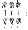
- Figures 2a - 2c are diagrams of losses in an example duplexer system.
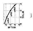
- Figure 3 is a chart of insertion loss tradeoffs in an example duplexer system.
- Figure 4 is a block diagram of an example electronic device.
- Figure 5 is a block diagram of an example electronic device with an example duplexer system.
- Figure 6 is a block diagram of an example electronic device with an example duplexer system.
- Figure 7 is a block diagram of an example electronic device with an example duplexer system.
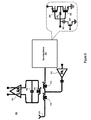
- Figure 8 is a block diagram of an example electronic device with an example duplexer system.
- Figure 9 is a block diagram of an example electronic device with an example duplexer system.
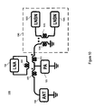
- Figure 10 is a block diagram of an example electronic device with an example duplexer system.
- Figure 11 is a block diagram of an example electronic device with an example duplexer system.
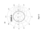
- Figure 12 is a diagram of an example Smith chart.
- Figure 13 is a block diagram of an example electronic device with an example duplexer system.
- Figure 14 is a block diagram of an example computer system that may be included with an electronic device.
- Figure 1 is an example of an electronic device 100.
- Electronic devices such as the electronic device 100, may, for example, be or include one or more of a cellular phone, a smart phone, a mobile phone, various other types of phones, a computer, a processor, a smart device, a personal digital assistant ("PDA"), a tablet, a storage device, a server, a device configured to communicate with one or more other devices or networks, or various other devices having a transmitter and a receiver.
- PDA personal digital assistant
- the electronic device 100 may include an antenna 110, through which the electronic device 100 may receive and transmit signals to one or more other devices, processors, receivers, antennas, or networks.
- the antenna 110 may be configured or otherwise operable to communicate or receive signals at many frequencies and over a wide range of frequencies.
- the antenna 110 may be configured to communicate over any cellular or radio frequencies.
- the electronic device 100 or antenna 110 may support, for example 3G / 4G bands I, II, III, IV, and IX. Other variations are possible.
- the electronic device 100 may include one or more receivers 120 ("RX").
- the one or more receivers 120 may be configured to detect and receive signals transmitted to or received by the electronic device 100.
- the receivers 120 may be configured to process signals received by the electronic device 100.
- the receiver 120 may receive signals at various power levels, such as at -110 dBm.
- the electronic device 100 may include one or more transmitters 130 ("TX").
- the one or more transmitters 130 may be configured to send or transmit one or more signals to the one or more other devices or networks, by or through the antenna 110.
- the transmitters 130 may, in some instances, operate using a frequency which may be different than the frequency used by the receiver 120.
- the transmitter 130 may be connected to one or more power amplifiers ("PA").
- the power amplifiers may be positioned between the transmitter 130 and the antenna 110 or between the transmitter 130 and a duplexer.
- the power amplifiers may amplify the power of a signal to be transmitted by the transmitter 130.
- the transmitter 130 may transmit signals at various power levels, such as at +28 dBm.
- the power levels of the receiver 120 and the transmitter 130 may be different.
- the electronic device 100 may include a duplexer 140.
- duplexers 140 may be or include an electronic balance duplexer ("EBD"), a division frequency duplexer, or other duplexers. Other examples of duplexers are possible.
- the duplexer 140 may enable the receiver 120 and the transceiver 130 to share or otherwise both use the antenna 110, and may enable the receiver 120 and the transmitter 130 to operate at the same time.
- the duplexer 140 may be configured to enable the electronic device 100 to receive and transmit at the same time.
- an EBD duplexer may perform electrical balance by subtracting a transmitting signal from an antenna input to isolate a receiver signal. This type of balancing may not assume or require any relationship between the RX and TX frequencies. Rather, the TX and RX signals may remain isolated even if they share a frequency band. Other examples are possible.
- Various electronic devices 100 such as a cell phone or Wi-Fi capable device, may have a duplexer 140 which may allow the electronic device 100 to receive and transmit signals at the same time.
- a 3G cellular phone may be or include a frequency division duplexing ("FDD") system where a transmitter 130 and a receiver 120 are both active simultaneously.
- FDD frequency division duplexing
- the duplexer 140 may include one or more filters, such as one or more bandpass filters or radio frequency (“RF") surface acoustic wave (“SAW”) filters. Each filter in the duplexer 140 may pass one or more frequency bands of a signal while attenuating noise at frequencies that are not passed. For example, a filter may allow frequencies of a signal with a range, such as between 2.1 GHz and 2.2 GHz, to pass, while rejecting or otherwise attenuating signals below 2.1 GHz and greater than 2.2 GHz. Other examples and filter types are possible.
- filters such as one or more bandpass filters or radio frequency (“RF") surface acoustic wave (“SAW”) filters.
- RF radio frequency
- SAW surface acoustic wave
- the receiver 120 may operate at a first frequency band, such as at 2.14 GHz, while the transmitter 130 may operate at a second frequency band, such as at 1.95 GHz.
- the duplexer 140 in this example may include two very sharp RF SAW filters - one RF SAW filter to pass the transmitting frequency band while filtering receiver band noise, and the other RF SAW filter to pass the receiving frequency band while filtering transmitter band noise. Other variations are possible.
- a duplexer 140 may be constructed in various ways or include various components.
- the duplexer 140 may be a three port duplexer 140, with one port for the antenna 110, one port for the receiver 120, and one port for the transmitter 130.
- the duplexer 140 may be arranged as a reciprocal circuit or reciprocal network with reciprocal circuit elements, such as resistors, capacitors, inductors, coupled inductors, or other circuit element that have interchangeable terminals.
- the duplexer 140 may, for example, be a 3-port lossy electronic balance duplexer ("EBD").
- S ESD_reciprocal may not be a unitary matrix and may represent the lossy network. Reciprocity may dictate or require that an insertion loss from any port to any other port be the same in both directions.
- Figures 2a - 2c show losses experienced for a 3-port duplexer.
- Figure 2a shows a 0dB insertion from transmitter to antenna, 100% of the power applied from the transmitter port is directed to antenna, and by reciprocity 100% of the power applied at the antenna is directed to the transmitter and 0% to the receiver. So 0dB insertion loss in the transmitter path results in infinite insertion loss for the receiver path.
- Fig. 2b shows the reverse case.
- Fig. 2c shows an alternative example where the incident power from the antenna is divided between the receiver and transmitter equally, 50% each. By reciprocity, 50% from the power applied from transmitter is directed to antenna, and since the transmitter and receiver are isolated, the remaining 50% of the power is dissipated in the duplexer.
- Figure 3 illustrates a graphical representation of the trade-off between the transmitter insertion loss and the receiver insertion loss for a reciprocal EBD such as duplexer 140.
- the power applied at any port in the 3-port duplexer 140 is divided between the two adjacent ports. Opposite ports are isolated.
- the receiver insertion loss (“RX IL”) equals the transceiver insertion loss (“TX IL”), and both equal 3dB.
- the EBD duplexer 140 can be altered such that the antenna favors either the receiver or the transmitter with lower loss for one, at the expense of higher loss for the other.
- An electronic device 100 may be configured or operable to receive signals at more than one frequency or frequency band.
- An electronic device 100 that receives signals at multiple different frequency bands may require a duplexer 140 for each supported frequency band.
- the electronic device 100 may need or use a specific or unique low noise amplifier (“LNA").
- LNA low noise amplifier
- FIG. 4 shows one example of a 2G / 3G radio frequency device 400.
- the 2G / 3G radio frequency device 400 may include an integrated circuit ("IC") 405 that may operate in a 2G / 3G cellphone.
- the IC 405 may support four 2G bands and three 3G bands.
- the IC 405 may include one or more of a radio frequency transceiver, four SAW filters (such as SAW filter 410), twelve matching components (such as matching component 420) needed for the 2G receiver (“2G RX"), and two power amplifiers ("PA”) for 2G.
- the IC 405 may also or alternatively include duplexers and PAs for 3G, which may dominate the area of the electronic device 400.
- Other examples of electronic devices 400 handling different frequencies are possible.
- duplexers 140, filters, and other hardware may need to be included with the electronic device.
- additional duplexers 140, filters, and other hardware may need to be included with the electronic device.
- new cell phones are produced and more frequency bands are used, expanding the size of the electronic device 400 with additional duplexers and filters may be difficult.
- electronic devices with an adjustable or tunable duplexer capable of handling different frequencies may be advantageous in reducing a number of necessary duplexers and size IC 405 used in the electronic device 400.
- FIG. 5 shows an example of a portion of an electronic device 500 with a duplexer system 550 (sometimes referred to as “duplexing system” or simply “duplexer”) that may be adjustable and tunable.
- the electronic device 500 may include an antenna 510, a power amplifier 520 connected or associated with the transmitter, and a low noise amplifier 530 (sometimes referred to as "LNA") connected or associated with the receiver.
- LNA low noise amplifier
- the low noise amplifier 530 may be removed or replaced by various other amplifiers, receivers, or other components.
- the duplexer system 550 and the low noise amplifier 530 may be interchanged or flipped in position, such that the low noise amplifier 530 may be connected with the antenna 510 and balancing network 540.
- Other variations are possible.
- the duplexer system 550 of the electronic device 500 may include a four port duplexer 505.
- the four port duplexer 505 may be a lossless reciprocal network.
- Each of the antenna 510, power amplifier 520, and low noise amplifier 530 may be connected to a different port of the duplexer 505.
- the fourth port termination of the duplexer 505 may be a balancing network ("BN") 540.
- the balancing network 540 may balance the power consumption such that the conservation of energy throughout the duplexer system 500 is satisfied.
- the duplexer system 550 may be arranged as a reciprocal circuit or reciprocal network with reciprocal circuit elements, such as resistors, capacitors, inductors, coupled inductors, or other circuit element that have interchangeable terminals.
- the duplexer system 550 may refer to the duplexer 505 and the balancing network 540. Other variations are possible.
- FIG. 6 shows the electronic device 500 with some example components of the duplexer 505.
- the duplexer 505 may, for example, include one or more inductor, such as the inductors 610, 615, and 620.
- Two inductors 610 and 615 may be arranged or configured between the antenna 510 and balancing network 540, with the power amplifier 520 connected between them.
- the inductors 610 and 615 may form a symmetry in the circuit.
- the inductors 610 and 615 may be two different inductors.
- the one large inductor may make up the two inductors 610 and 615.
- the power amplifier 520 may be attached to a point between the one large inductor, creating two separate inductors 610 and 615 on either side of the point at which the power amplifier 520 is connected.
- the two inductors 610 and 615 may be identical.
- the two inductors 610 and 615 may have different inductances, which may depend on where the power amplifier is connected.
- Other examples of inductors 610 and 615 are possible.
- the low noise amplifier 530 may additionally include an inductor 620 of the duplexer 505.
- the arrangement and properties of the inductors 610, 615, and 620, such as the impedance or number of turns in the inductors 610, 615, and 620, may operate to attenuate a power output from the power amplifier 520 before the signal reaches the low noise amplifier 530.
- the inductors 610, 615, and 620 may operate as a transformer (such as an autotransformer). Other configurations or examples of duplexers 505 and duplexer components are possible.
- An antenna 510 of an electronic device 500 may have varying impedance values.
- the antenna 510 may have a different impedance value depending on what frequency a signal is that the antenna 510 is communicating with and the physical surrounding of the antenna affecting the near field.
- the duplexer system 550 may implement or use a passive or active balancing network 540 which may be tunable or adjustable.
- the balancing network 540 may be used to match an antenna impedance and/or isolate the power amplifier 520 from the low noise amplifier 530.
- the balancing network 540 may have or include one or more adjustable or modifiable capacitance or inductance components or adjustable or modifiable resistance components.
- the modifiable or tunable balancing network 540 may beneficially enable the duplexer system 550 to isolate the power amplifier 520 and the low noise amplifier 530 for many different frequencies and antenna impedances.
- the duplexer system 550 may thus be, include, or represent a multi-band duplexer, and may be capable of performing duplexing that would otherwise require multiple duplexers 140.
- the use of a duplexer system 550 that is configured or operable to be adjusted and used for handling various receiving frequencies may offer flexibility in electronic device design and reduce a number or amount of components needed in designing communication devices.
- a passive balancing network 540 may be a network made up of elements that may not need or require any bias current or voltage to operate.
- a passive balancing network may include one or more inductors, capacitors, resistors, and metal-oxide semiconductor ("MOS") switches.
- MOS metal-oxide semiconductor
- the 4-port lossless reciprocal network with a resistor for the balancing network 540 may have an S-matrix given by: Where S 12 and S 13 satisfy
- 2 1.
- a receiver insertion loss may add directly to a receiver cascaded noise figure (sometimes referred to as "RX NF").
- FIG. 7 shows an example of an electronic device 700 with a duplexer system 550 having a passive balancing network 740.
- the balancing network 740 may include one or more capacitor 750 (sometimes referred to as “capacitance component”) and resistor 760 (sometimes referred to as “resistance component” or “resistive component”). While only one capacitor 750 and one resistor 760 are shown, an active balancing network 740 may include a set of multiple resistors which may, for example, be selected or connected using one or more switches, and a set of multiple capacitors which may, for example, be selected or connected using one or more switches.
- the balancing network 740 may include a switchable bank of ten (or any number) resistors of different resistance values, any one or more of which may be selected and connected to obtain a given resistance value, and also may include a switchable bank of five (or any number) capacitors of different capacitance values, any one or more of which may be selected and connected to obtain a desired capacitance value.
- the one or more capacitor 750 and resistor 760 may be connected in parallel, series, or some combination of parallel and series. Each capacitor 750 may contribute a capacitance or reactive impedance to an overall impedance of the balancing network 740. Each resistor 760 may contribute a resistance or real impedance to an overall impedance of the balancing network 740.
- the balancing networks may additionally or alternatively include one or more inductors or an inductive component which may contribute to an overall impedance of the balancing network. Other variations of balancing networks 740 are possible.
- the adjustable network 740 may also or alternatively include one or more switches 770 and 775, which may be used to control a capacitance or resistance value of the overall impedance of the balancing network 740.
- the one or more switches of a balancing network 740 may be made or created using one or more Complementary metal-oxide-semiconductor ("CMOS").
- CMOS Complementary metal-oxide-semiconductor
- CMOS Complementary metal-oxide-semiconductor
- CMOS Complementary metal-oxide-semiconductor
- a balancing network 740 may include one or more adjustable or modifiable capacitor as the capacitance component and/or an adjustable or modifiable resistor as the resistance component.
- the adjustable or modifiable capacitor may have or contribute a capacitance to an impedance of the balancing network 740.
- the modifiable capacitor may be monitored, adjusted, modified, or otherwise changed to contribute a capacitance value to an overall impedance of the balancing network 740.
- the adjustable or modifiable resistor may have or contribute a resistance to an impedance of the balancing network 740.
- the modifiable resistor may be monitored, adjusted, modified, or otherwise changed to contribute a resistance value to an overall impedance of the balancing network 740.
- the balancing network 740 may be configured or operable to control the impedance of the balancing network 740. As such, the balancing network 740 may be modified, adjusted, or altered to provide many different impedance values.
- a processor, logic, computer readable medium with instructions, or a controller may be configured or operable to monitor, determine, set, or otherwise control the adjustable capacitance and adjustable resistance of the balancing network 740, thereby setting and adjusting an overall impedance of the balancing network 740.
- the adjustable impedance of the balancing network 740 may be used in various ways.
- the impedance of the balancing network 740 may be adjusted or modified to isolate the power amplifier 520 from the low noise amplifier 530. Where the power amplifier 520 is isolated from the low noise amplifier 530, half of the power in the duplexer 505 is spent, burned, or used in the components of the antenna 510, and the other half are spent, burned, or used in the balancing network 540. Continuous infinite isolation of the power amplifier 520 and low noise amplifier 530, regardless of a frequency or changing impedance of an antenna 510, may be accomplished in various ways, such as by ensuring that the voltage difference between the inductors 610 and 615 is zero, or minimized.
- the balancing network 740 may monitor and adjust the balancing network impedance continuously, nearly continuously, at intervals, during or after certain periods of time, when prompted, when triggered, or at various other times.
- the inductors 610 and 615 of duplexer 505 may be identical or have the same impedance.
- the balancing network 740 may perform isolation by monitoring the variable impedance of the antenna 510 (sometimes referred to as "antenna impedance").
- the impedance of the balancing network 740 may be adjusted, such as by a controller or processor, to be the same as the monitored impedance of the antenna 510.
- the impedance of the balancing network 740 may thus mirror, track, and mimic any changes in impedance of the antenna 510.
- the impedance of the balancing network 740 may also change to track the change in the antenna impedance. In doing so, the balancing network 740 may ensure that a voltage drop over the antenna 510 is the same as the voltage drop over the balancing network 740. If the voltage drops over the antenna 510 and the balancing network 740 are the same, the difference between the voltages between the two identical inductors 610 and 615 may be zero and the power amplifier 620 may be isolated from the low noise amplifier 640. In this way, the duplexer system 550 may be tunable or adjustable to accommodate communications with the antenna 510 at various different frequencies or frequency bands.
- the impedances of the two inductors 610 and 615 may not be identical.
- one inductor 610 may have an inductance of N1 while the second inductor 615 may have a second, different inductance N2.
- the balancing network 740 may ensure a zero voltage difference between the inductors 610 and 615 in various other ways.
- the balancing network 740 may continue to monitor the impedance of the antenna 510 or a voltage drop over the antenna 510. However, because the impedances of the inductors 610 and 615 may be different, the balancing network 740 may not achieve isolation of the low noise amplifier 530 by merely mimicking the impedance of the antenna 510. Rather, the balancing network 740 or a controller of the balancing network may apply one or more algorithms or functions which factor in the differences between the known impedances of the inductors 610 and 615.
- the algorithms or functions may be used to calculate or otherwise determine an impedance of the balancing network 740 which will create a zero voltage difference and isolate the low noise amplifier 530 and the power amplifier 520.
- a voltage difference between the inductors 610 and 615 may be measured directly, and the impedance of the antenna 510 may be ignored.
- the balancing network 740 or a controller of the balancing network 740 may apply one or more algorithms or functions which may factor the measured voltage drop and the known impedances of the inductors 610 and 615 to calculate a necessary change in the balancing network 740 to create a zero voltage drop.
- Other examples and methods of isolating the low noise amplifier 530 and the power amplifier 520 are possible.
- Isolation may, in some implementations, be limited by the resolution of the balancing impedance. Where an adjustable capacitance component and an adjustable resistive component are included in the balancing network 740, isolation may only be limited by limits of the adjustability of the capacitance component and the resistive component. Where the balancing network 740 is implemented as variable impedance using switchable banks of resistors and capacitors, the impedance may be limited by the available combinations of resistors and capacitors in the switchable banks.
- the electronic device 700 may have various properties, such as a transmitter insertion loss, a receiver insertion loss, and a receiver noise figure (sometimes referred to as "RX NF").
- the transmitter insertion loss may refer to an amount of power that goes to an antenna 510 from power that is output from a power amplifier 520.
- the receiver insertion loss may refer to an amount of power that goes to the low noise amplifier 530 from the power coming from the antenna 510.
- an electronic device 700 may be operable to provide small insertion losses or noise figures.
- the transmitter insertion loss and receiver insertion loss of an electronic device 700 may have or experience a tradeoff, as shown in Figure 3 .
- An increase in the inductance of one of the inductors 610 or 615 will shift the tradeoff, such that one of the insertion losses (either TX or RX) will improve while the other insertion loss (RX or TX) will be worse.
- the receiver noise figure may be a more important parameter than a receiver insertion loss.
- an operator of a receiver may be more interested in a signal-to-noise ratio than an absolute power level.
- the receiver noise figure may refer to or provide an indication of how much noise the receiver is receiving and how sensitive the receiver is.
- the receiver noise figure may vary with or otherwise be directly related to the resistance of the balancing network 740.
- the receive noise figure may indicate a resistance seen at the low noise amplifier 530.
- the resistance at the low noise amplifier 530 may include a resistance from the antenna 510, and a resistance from the balancing network 740.
- a resistance in a passive balancing network may be varied or adjusted in a limited number of ways, such as by either adjusting a set resistance for the passive balancing network or according to environmental changes, such as a temperature.
- the balancing network 740 may have little or no freedom to change the noise figure once a resistance is set for the isolation.
- the receiver insertion loss may add directly to a receiver cascaded noise function, because the duplexer system 550 is passive, and regardless of implementation, the available noise power will depend only on the real part of the impedance of the balancing network 740.
- the transmitter insertion loss and the receiver noise figure may be optimized by having identical inductors 610 and 615, such that the transceiver loss is around 3 dB and the noise figure is minimized.
- an active balancing network may include one or more active elements which may use or require a bias voltage or current (for example, a direct current (“DC") bias current).
- an active balancing network may include active components or active elements ("active components") like MOS transistors operating as transconductors and amplifiers or various other transistors. Active elements may be driven, powered, operated, or otherwise controlled using a bias current or voltage, which may control or initiate the transconductance of the active elements or components.
- the active balancing network 540 may also include one or more passive elements.
- One or more components of an active balancing network 540 may be configured or operable to tolerate large voltage swings.
- a duplexer system with an active balancing network may be configured and operable achieve a noise figure of less than 3 dB and overcome a physical 3 dB limit.
- FIG 8 shows an example of an electronic device 800 with a duplexer system having an active balancing network 840.
- the electronic device 800 may additionally or alternatively include one or more of an antenna 510, a power amplifier 520, a low noise amplifier 530, inductors 610, 615, and 620, and a capacitor 790 which may be the same as or similar to the antenna 510, power amplifier 520, low noise amplifier 530, inductors 610, 615, and 620, and capacitor 790 of the electronic device 700.
- the balancing network 840 may be a low noise balancing network.
- the low noise balancing network 840 may be configured and operable to enable the electronic device 800 to operate with very low loss.
- the balancing network 840 may include or contain one or more passive components, such as one or more switch, capacitor 850, and resistor 860.
- the active balancing network 840 may include one or more active components, such as one or more transistors 880, 885, and 890. Examples of transistors that may be used or included with active balancing networks 840 may be or include a metal-oxide-semiconductor field-effect transistor ("MOSFET”), CMOS, junction gate field-effect transistors (“JFETs”), bi-polar junction transistors (“BJTs”) or other transistors.
- Active balancing networks 840 may be constructed or operable with various technologies, such as silicon, SOI, GaAs, InP, GaN, and various other technologies.
- the balancing network circuitry shown in Figure 8 is one example of an active balancing network.
- Other examples may include, for example, an inductively generated common source (“CS") LNA, a common gate LNA, a common-gate LNA with feedback, a CS LNA with buffered feedback, or various other implementations.
- CS common source
- Various other circuits or combinations of components may be used to create active balancing networks 840.
- a impedance of the active balancing network 840 may, for example, depend on a transconductance g mp and g mn of the transistors 880 and 885.
- the transconductance g mp and g mn of the transistors 880 and 885 may vary with changes in bias current or bias voltage of the balancing network 840.
- a resistance and impedance of the balancing network 840 may thus be variable by changing the bias current or bias voltage of the active components of the balancing network, thereby changing an impedance of the active components.
- the transconductance of the transistors 880, 885, and 890 in the balancing network 840 may be controlled and modified to produce a desired resistance value.
- the active components of the balancing network 840 may enable the balancing network 840 to control and provide a minimum resistance value of the balancing network 840, while matching an antenna impedance or isolating the power amplifier 520 from the low noise amplifier 530.
- the balancing network 840 may enable a noise figure which may break the 3 dB theoretical noise limit.
- one or more of the inductors 610 and 615 may be modified to provide for a low transceiver insertion loss at the expense of a high receiver insertion loss.
- a turns ratio of the two inductors 610 and 615 may be skewed by moving a tapping point (point which the power amplifier 520 connects between the two inductors 610 and 615) from the center (where the two inductors 610 and 615 are identical) to have different inductances of the two inductor spirals 610 and 615.
- the transceiver insertion loss may be lowered to 2.5 dB, for example, at the expense of higher insertion loss for the receiver of 4.6 dB.
- the inductors 610 and 615 may, for example, be placed or realized in the uppermost layers of metal.
- the active balancing network 840 may operate to provide a resistance value based on the transconductance of the transistors 880, 885, and 890, the receiver noise figure may also be reduced. Since the noise voltage of the balancing network and the antenna appears differentially at the input of the low noise amplifier 530, the effective noise figure of the duplexer will be smaller, such as 1dB. Physically, this reduced receiver noise figure may be obtained by spending, burning, or otherwise using more current as a bias current in one or more active components, such as the transistors 880, 885, and 890, in the balancing network 840. In this way, for example, it is possible with a passive 4-port duplexer and an active balancing network 840 to break the 3-dB performance limitation.
- the balancing network 840 may realize a resistance value with a lower noise figure than in a passive balancing network.
- the quality factor of the elements in the balancing network 840 may only affect the insertion loss, but may not affect the isolation so long as a balance may be achieved.
- Figure 9 shows an electronic device 900 which may be similar to or resemble one or more of the electronic devices 700 and 800.
- the electronic device 900 may have an antenna 510, power amplifier 520, low noise amplifier 830, inductors 610 and 615 of a duplexer 505, and balancing network 940.
- the duplexer 505 may or may not be directly connected to the antenna 510 without any matching elements.
- the balancing network 940 may be a passive balancing network, such as the balancing network 740, or may be an active balancing network, such as the balancing network 840.
- the electronic device 900 shows one possible set of circuitry for the low noise amplifier 530.
- the electronic device 900 may differ from the electronic devices 700 and 800 in that the low noise amplifier 930 of the electronic device 900 may be or have a common source low noise amplifier 930, rather than an impedance matched low noise amplifier 530.
- the common source low noise amplifier 930 may offer, for example, 6 dB more gain than an impedance-matched low noise amplifier.
- both the duplexer 505 and the low noise amplifier 530 may be integrated on the same chip.
- the components of the electronic device 900 may be integrated on a prototype chip that may integrate the inductors 610 and 615, the low noise amplifier 930, the balancing network 940, and digital control circuitry.
- the components of the electronic device 900 may be fabricated in a TSMC 65nm CMOS technology, with the duplexer 505 occupying an area of 0.2mm 2 dominated by the two inductors - one being the duplexer autotransformer, and the other being the LNA load.
- Various other examples of circuitry for a low noise amplifier 530 are possible.
- the electronic devices 500, 700, 800, and 900 with the balancing networks 540, 740, 840, and 940 may allow a duplexer system to operate, duplex, or otherwise process many different frequencies that may be communicated with the antenna 510.
- the multi-band duplexer systems in the electronic devices 500, 700, and 800 may isolate the power amplifier 520 and the low noise amplifier 530 for many different frequencies and antenna impedances.
- the duplexer system 550 may provide for a reduction in a number of duplexers needed for an electronic device communicating over many different frequencies, and provides increased flexibility in electronic device design.
- an electronic device may communicate (such as transmit or receive) using signals with large power swings, such as, for example, plus-or-minus 7.5 V, or 15 V peak-to-peak.
- signals with large power swings such as, for example, plus-or-minus 7.5 V, or 15 V peak-to-peak.
- An example may be a cellular phone operating at a 3G standard that may specify a maximum output power level of 24 dBm at the antenna 510 for a typical peak-to-average ratio of 3.2 dB, with an antenna peak-to-peak voltage of about 15 V.
- Figure 10 illustrates an example electronic device 1000 with a balancing network 1040 that may be used with large power supplies without damaging components of the balancing network 1040.
- the electronic device 1000 may be similar, resemble, or include some of the features of electronic devices 500, 700, 800, or 900.
- the electronic device 1000 may include an antenna 510, a power amplifier 520, a low noise amplifier 530, and inductors 610, 615, and 620.
- the duplexer system of the electronic device 1000 may additionally include a balancing network 1040 which may account for large voltages and large signals.
- the balancing network 1040 may include one or more transformers or inductors 1010 and 1015. Where the electronic device 1000 and antenna 510 communicate large signals having large power or voltage levels or swings, such as plus-or-minus 7.5 V, an equivalent voltage drop (when the inductors 610 and 615 are identical) or a similar voltage drop (otherwise) may occur over the inductor 1010.
- the inductors 1010 and 1015 may operate to drop a voltage from a first voltage level V1 over the inductor 1010 (such as plus-or-minus 7.5 V) to a second voltage level V2 over the inductor 1015 which may be a fraction of the first voltage level.
- the voltage may be, for example, halved through the use of the inductors 1010 and 1015.
- the voltage ratio V1 : V2 may, for example, be the same as or reflect the difference in the number of turns in the inductor 1010 (N1) to the number of turns in the inductor 1015 (N2).
- other transformers may be implemented in the balancing network to step down the voltage from the duplexer or inductor 615, or the voltage may be reduced in other ways and by other amounts.
- the balancing network 1040 may additionally include one, two, or more low noise balancing networks 1020 and 1025 (sometimes referred to as "balancing circuits"). Each of the two low noise balancing networks 1020 and 1025 may be attached or connected to one end of the inductor 1015 of the transformer.
- the low noise balancing networks 1020 and 1025 may be the same or identical, or may be different from each other.
- Each of the low noise balancing networks 1020 and 1025 may be the same as, resemble, or include one or more components also included in the balancing network 740, 840, or 940.
- the low noise balancing network 1020 may include one or more adjustable or modifiable capacitors, resistors, and switches, as well as one or more active transistors, such as in the balancing network 940.
- the low noise balancing networks 1020 and 1025 are each substantially the same active balancing networks, and both may be substantially the same as the active balancing network 940. Other variations are possible.
- each of the low noise balancing networks 1020 and 1025 may be adjusted or modified in parallel or otherwise at the same time and in the same amount, or may be controlled and modified separately and differently.
- the low noise balancing networks 1020 and 1025 may not be low noise, and may be simply referred to as balancing networks or balancing circuits. Other variations are possible.
- the voltage at each of the low noise balancing networks 1020 and 1025 may be cut in half or otherwise reduced. Stepping down the voltage applied to the components of the balancing network 1040 may protect the components of the balancing networks 1020 and 1025 from being damaged.
- a voltage drop of plus-or-minus 7.5 V observed at the inductor 1010 may be reduced by, for example, a factor of 4 (halved at the inductor 1015; and halved again by using two balancing networks 1020 and 1025), and generate a voltage for the balancing networks of less than 2 V.
- a reduction in voltages at the balancing networks 1020 and 1025 may be especially valuable, for example, where the balancing networks are composed of or otherwise include CMOS switches or other CMOS technology which may not otherwise tolerate large voltage levels.
- the balancing network 1040 increases a power and size of a signal that the duplexer system of electronic device 1000 can communicate. This may allow the electronic device 1000 to communicate large signals and operate at a high voltage level. Other examples and benefits are possible.
- FIG 11 illustrates another example of an electronic device 1100.
- the electronic device 1100 may be similar, resemble, or include some of the features of electronic devices 500, 700, 800, 900, or 1000.
- the electronic device 1100 may include an antenna 510, a power amplifier 520, a low noise amplifier 530, and a duplexer 505.
- the electronic device 1200 may also include one or more balancing networks 1140.
- the balancing network 1140 may be similar to or resemble any of the balancing networks 540, 740, 840, 940, or 1040, or may be different.
- the electronic device 1100 may include an antenna tracking unit ("ATU") 1120.
- the antenna tracking unit 1120 may be used, for example for tracking and providing a tuning of an impedance of an antenna 510.
- An antenna impedance may change slowly as a near-field of the antenna 510 is perturbed or changed.
- one or more industry specifications may specify an acceptable antenna impedance variation.
- an industry specification may specify a voltage standing wave ratio (VSWR) of 3:1 for an antenna impedance variation.
- Figure 12 shows an example of a Smith chart 1200 showing impedances and a VSWR circle.
- a balancing network 1140 may be configured and operable to track impedance variations of an antenna 510 around a center of the Smith chart 1200 with fine resolution.
- the antenna tuning unit 1120 may be implemented as a pi network, with an off-chip inductor and two on-chip capacitor banks.
- the antenna tuning unit 1120 may be added to improve the efficiency of the power amplifier 520 and protect the power amplifier 520 from breakdown under one or more antenna mismatch conditions.
- the antenna tuning unit 1120 may transform the antenna impedance into the shaded area, where the balancing network 1240 can balance the duplexer 505.
- the antenna tracking unit 1120 may be configured in various other ways.
- FIG. 13 illustrates one example of an electronic device 1300.
- the electronic device may include an antenna-ready radio integrated partially or completely on a single CMOS chip.
- the electronic device 1300 may include one or more of a multi-mode multi-band power amplifier 1310, a multi-band RF filter 1320, and a multi-band duplexer system 1330.
- the multi-band RF filter 1320 may be configured or operable for use with time division duplexing ("TDD") systems such as 2G Global System for Mobile Communications (“2G GSM").
- TDD time division duplexing
- 2G GSM 2G Global System for Mobile Communications
- the multi-band duplexer system 1330 may be configured or operable for use with frequency division duplexing ("FDD") systems such as 3G Wideband Code Division Multiple Access (“WCDMA”) systems.
- the multi-band duplexer systems 1330 may, for example, be, include, or represent one or more of the duplexer systems 550 and balancing networks 540, 740, 840, 940, 1040, and1140 discussed.
- Some or all of the components of the electronic device 1300, such as the multi-band duplexer 1330 may be manufactured and used in various other electronic devices, such as in electronic devices 100, 500, 700, 800, 900, or 1000 to improve efficiency, save space, and reduce costs.
- an electronic device may implement the duplexer system and balancing network as a frequency independent CMOS RF duplexer for 3G / 4G cellular applications.
- the CMOS RF duplexer may be a wideband integrated RF duplexer, which may support 3G / 4G bands I, II, III, IV and IX, and may achieve a TX-to-RX isolation of more than 55 dB in a transmit-band, and greater than 45 dB in a corresponding receive-band across 200 MHz of bandwidth.
- a 65 nm CMOS duplexer / LNA may be implemented and achieve a transmit insertion loss of 2.5 dB, and a cascaded receiver noise figure of 5 dB with more than 27 dB of gain.
- Other examples and configurations of electronic devices using a duplexing system are possible.
- a duplexer 505 or duplexer systems 550 used in any of the electronic devices 500, 700, 800, 900, 1000, or 1100 may have various properties and expectations.
- the duplexer 505 or duplexer system 550 may have a transceiver leakage at an associated low noise amplifier.
- S leakage is the transceiver leakage power density at receiver input in dBm/Hz
- S PA is the power amplifier output power density in dBm/Hz
- ISO is the duplexer transceiver-to-receiver isolation in dB.
- Other properties and examples are possible.
- the duplexer 505 or duplexing system 550 in the electronic devices 500, 700, 800, 900, 1000, and 1100 may be configured to provide some isolation, such as 50dB or more of isolation, in a transmitting (or transceiver) band.
- the duplexer 505 or duplexing system 550 may also or alternatively avoid saturating the receiver or damaging the LNA, and may relax the linearity and phase noise requirements of the receiver.
- the duplexer 505 or duplexing system 550 may also be configured to attenuate the noise in the receiving (or receiver) band, such as attenuating the noise by about 45dB to push it below a receiver noise floor.
- the duplexer 505 or duplexer system 550 may be configured to provide that isolation while introducing minimal insertion loss ("IL") in both the transmitter and receiver paths.
- IL minimal insertion loss
- the power amplifier may burn or use more power to put out a higher power to overcome the transmitter insertion loss, while the receiver IL may subtract directly from receiver sensitivity.
- the duplexer 505 or duplexer system 550 may be configured to tolerate a large PA output swing, such as an output swing of up to 15V peak-to-peak.
- the duplexer 505 or duplexer system 550 may be configured to provide isolation for multiple bands, one band at a time.
- Insertion loss of duplexers with SAW filters may vary from band to band. Insertion loss may vary depending on the frequency separation between a receiving frequency band and a transmitting frequency band. Insertion loss may, for example, be about 2dB for a transmitting frequency path, and 2.5dB for the receiving frequency path, such as, for example, because of the higher isolation requirement.
- Duplexer systems such as duplexer system 550, may incorporate one or more of the active balancing networks 840, 940, 1040, and 1140 to obtain a desired and adjustable or tunable impedance.
- the duplexer systems may achieve an isolation of the power amplifier 520 and the low noise amplifier 530 at any signal or any frequency without assuming anything about the frequency.
- the active balancing networks 840, 940, 1040, and 1140 may achieve a lower noise for the same impedance compared to a passive implementation, and may break a theoretical 3-dB noise function performance limitation.
- the receiver noise figure of an electronic device using a duplexer system 550 with one or more of the active balancing networks 840, 940, 1040, and 1140 may be less than a receiver insertion loss.
- the active balancing networks 840, 940, 1040, and 1140 may directly improve the receiver performance, or the improvement may be distributed between the receiver and transmitter.
- the absence of any linear transconductor in the implementation may alleviate low breakdown voltages.
- the balancing network 1040 may be used to step down voltage levels and limit voltage swings experienced by the low noise balancing networks 920 and 925. Other benefits and advantages are possible.
- One or more functions of an electronic device may have, include, or access a process or computer system, such as computer system 1400 shown in Figure 14 .
- a processor or computer system may be included with an electronic device and may be implemented to monitor an antenna impedance or adjust one or more components of a balancing network 540, 740, 840, 940, 1040, or 1140.
- Such computer systems may include a set of instructions that can be executed to cause the computer system 1400 to perform any one or more of the methods or computer based functions disclosed herein.
- the computer system 1400 may operate as a standalone device or may be connected, e.g., using a network, to other computer systems or peripheral devices.
- a computer system 1400 may also be implemented as or incorporated into various devices, such as a personal computer (PC), a tablet PC, a set-top box (STB), a personal digital assistant (PDA), a mobile device, a palmtop computer, a laptop computer, a desktop computer, a communications device, a wireless telephone, a land-line telephone, a control system, a camera, a scanner, a facsimile machine, a printer, a pager, a personal trusted device, a web appliance, a network router, switch or bridge, or any other machine capable of executing a set of instructions (sequential or otherwise) that specify actions to be taken by that machine.
- PC personal computer
- PDA personal digital assistant
- the computer system 1400 may include a processor 1402, such as a central processing unit (CPU), a graphics processing unit (GPU), or both.
- the processor 1402 may be a component in a variety of systems.
- the processor 1402 may be part of a standard personal computer or a workstation.
- the processor 1402 may be one or more general processors, digital signal processors, application specific integrated circuits, field programmable gate arrays, servers, networks, digital circuits, analog circuits, combinations thereof, or other now known or later developed devices for analyzing and processing data.
- the processor 1402 may implement a software program, such as code generated manually (i.e., programmed).
- the computer system 1400 may include a memory 1404 that may communicate via a bus 1408.
- the memory 1404 may be a main memory, a static memory, or a dynamic memory.
- the memory 1404 may include, but is not limited to computer readable storage media such as various types of volatile and non-volatile storage media, including but not limited to random access memory, read-only memory, programmable read-only memory, electrically programmable read-only memory, electrically erasable read-only memory, flash memory, magnetic tape or disk, optical media and the like.
- the memory 1404 may be operable to store instructions executable by the processor 1404.
- the functions, acts or tasks illustrated in the figures or described herein may be performed by the programmed processor 1404 executing the instructions stored in the memory 1404.
- the functions, acts or tasks may be independent of the particular type of instructions set, storage media, processor or processing strategy and may be performed by software, hardware, integrated circuits, firm-ware, micro-code and the like, operating alone or in combination.
- processing strategies may include multiprocessing, multitasking, parallel processing and the like.
- the computer system 1400 may further include a display unit 1410, such as a liquid crystal display (LCD), an organic light emitting diode (OLED), a flat panel display, a solid state display, a cathode ray tube (CRT), a projector, a printer or other now known or later developed display device for outputting determined information.
- a display unit 1410 such as a liquid crystal display (LCD), an organic light emitting diode (OLED), a flat panel display, a solid state display, a cathode ray tube (CRT), a projector, a printer or other now known or later developed display device for outputting determined information.
- the display 1410 may act as an interface for the user to see the functioning of the processor 1402, or specifically as an interface with the software stored in the memory 1404 or in the drive unit 1416.
- the computer system 1400 may include an input device 1412 configured to allow a user to interact with any of the components of system 1400.
- the input device 1412 may be a number pad, a keyboard, or a cursor control device, such as a mouse, or a joystick, touch screen display, remote control or any other device operative to interact with the computer system 1400.
- the computer system 1400 may also or alternatively include a disk or optical drive unit 1416.
- the disk drive unit 1416 may include a computer-readable medium 922 in which one or more sets of instructions 1424, e.g. software, can be embedded. Further, the instructions 1424 may embody one or more of the methods or logic as described herein. The instructions 1424 may reside completely or partially within the memory 1404 and/or within the processor 1402 during execution by the computer system 1400.
- the memory 1404 and the processor 1402 also may include computer-readable media as discussed above.
- a computer-readable medium 1422 includes instructions 1424 or receives and executes instructions 1424 responsive to a propagated signal so that a device connected to a network 1426 can communicate voice, video, audio, images or any other data over the network 1426.
- Instructions 1424 may be transmitted or received over the network 1426 via a communication port or interface 1420, and/or using a bus 1408.
- the connection with the network 1426 may be a physical connection, such as a wired Ethernet connection or may be established wirelessly as discussed below.
- the additional connections with other components of the system 1400 may be physical connections or may be established wirelessly.
- the network 1426 may alternatively be directly connected to the bus 1408.
- While the computer-readable medium 1422 is shown to be a single medium, the term “computer-readable medium” may include a single medium or multiple media, such as a centralized or distributed database, and/or associated caches and servers that store one or more sets of instructions.
- the term “computer-readable medium” may also include any medium that is capable of storing, encoding or carrying a set of instructions for execution by a processor or that cause a computer system to perform any one or more of the methods or operations disclosed herein.
- the computer-readable medium 1422 may be non-transitory, and may be tangible.
- the computer-readable medium 1422 can include a solid-state memory such as a memory card or other package that houses one or more non-volatile read-only memories.
- the computer-readable medium 1422 can be a random access memory or other volatile re-writable memory. Additionally or alternatively, the computer-readable medium 1422 can include a magneto-optical or optical medium, such as a disk or tapes or other storage device to capture carrier wave signals such as a signal communicated over a transmission medium.
- a digital file attachment to an e-mail or other self-contained information archive or set of archives may be considered a distribution medium that is a tangible storage medium. Accordingly, the disclosure is considered to include any one or more of a computer-readable medium or a distribution medium and other equivalents and successor media, in which data or instructions may be stored.
- dedicated hardware implementations such as application specific integrated circuits, programmable logic arrays and other hardware devices, can be constructed to implement one or more of the methods described herein.
- Applications that may include the apparatus and systems of various embodiments can broadly include a variety of electronic and computer systems.
- One or more embodiments described herein may implement functions using two or more specific interconnected hardware modules or devices with related control and data signals that can be communicated between and through the modules, or as portions of an application-specific integrated circuit. Accordingly, the present system encompasses software, firmware, and hardware implementations.
- the methods described herein may be implemented by software programs executable by a computer system.
- implementations can include distributed processing, component/object distributed processing, and parallel processing.
- virtual computer system processing can be constructed to implement one or more of the methods or functionality as described herein.
Landscapes
- Engineering & Computer Science (AREA)
- Computer Networks & Wireless Communication (AREA)
- Signal Processing (AREA)
- Power Engineering (AREA)
- Amplifiers (AREA)
- Transceivers (AREA)
Description
- This disclosure relates to systems and methods (generally referred to as systems) utilizing an adjustable duplexer system. More specifically, this disclosure relates to phones or radios utilizing a tunable multi-band duplexer system with an active balancing network.
- Electronic devices communicate with each other in various ways. For example, electronic devices may transmit or receive electro-magnetic signals carrying information or data. The electro-magnetic signals may be transmitted or received at one or more frequencies. As communication networks become more complex, it may be desirable for electronic devices to be able to communicate with each other over or using different frequencies while maintaining compact or efficient dimensions.
- According to an aspect, a duplexing system for an electronic device comprises:
- a duplexer connected with an antenna;
- a balancing network connected with the duplexer and having an adjustable network impedance, the balancing network including an active component; and
- where the balancing network is configured to adjust the network impedance to match an antenna impedance of the antenna.
- Advantageously, the balancing network further includes a transformer connected with the duplexer and a balancing circuit.
- Advantageously, the transformer receives a first voltage from the duplexer and outputs a second voltage to the balancing network based on the first voltage, the second voltage lower than the first voltage.
- Advantageously, the balancing network includes two balancing circuits connected to the transformer.
- Advantageously, the two balancing circuits include substantially the same components.
- Advantageously, the balancing network matches the antenna impedance and minimizes a resistance of the active component.
- According to an aspect, an electronic device comprises:
- a duplexer including a first port, a second port, a third port, and a fourth port;
- an antenna having an antenna impedance, the antenna connected to the first port;
- a power amplifier configured to amplify a transmission signal to be transmitted by the antenna, the power amplifier connected to the second port;
- a low noise amplifier configured to amplify a reception signal received by the antenna, the low noise amplifier connected to the third port;
- a balancing network having a balancing network impedance, the balancing network connected to the fourth port, the balancing networking including an active component;
- where the balancing network adjusts the balancing network impedance to match the antenna impedance to isolate the power amplifier and the low noise amplifier.
- Advantageously, the balancing network comprises an adjustable resistive component and an adjustable capacitive component.
- Advantageously, the balancing network adjusts the balancing network impedance to match the antenna impedance by modifying a capacitance of the adjustable capacitive component.
- Advantageously, the balancing network comprises a transformer having a first inductor connected to the fourth port and a second inductor having a first end and a second end.
- Advantageously, the balancing network further comprises a first balancing circuit connected to a first end of the second inductor, and a second balancing circuit connected to a second end of the second inductor.
- Advantageously, the first balancing circuit and the second balancing circuit include substantially the same components.
- Advantageously, the balancing network impedance is adjusted by controlling a bias current or bias voltage of the active component.
- Advantageously, the transformer is configured to provide, from a first voltage over the first inductor, a second voltage over the second inductor, where the first voltage over the first inductor is greater than the second voltage over the second inductor.
- According to an aspect, a method of isolating a power amplifier comprises:
- monitoring an antenna impedance; and
- adjusting a balancing network impedance based on the antenna impedance to provide a zero voltage difference at a point where a power amplifier is connected to a duplexer, including adjusting an active component impedance of an active component in a balancing network.
- Advantageously, adjusting the balancing network impedance comprises adjusting a bias current or voltage of the active component to balance the antenna impedance with the balancing network impedance.
- Advantageously, the method further comprises minimizing a resistance of the active component of the balancing network while balancing the antenna impedance with the balancing network impedance.
- Advantageously, the method further comprises controlling a transmitter insertion loss and a receiver insertion loss by setting the receiver insertion loss greater than the transmitter insertion loss.
- Advantageously, adjusting the balancing network impedance comprises adjusting a first circuit impedance of a first balancing circuit and adjusting a second circuit impedance of a second balancing circuit.
- Advantageously, the adjustment to the first circuit impedance is substantially the same as the adjustment to the second circuit impedance.
- The system may be better understood with reference to the following drawings and description. In the figures, like reference numerals designate corresponding parts throughout the different views.
-
Figure 1 is a block diagram of an example electronic device. -
Figures 2a - 2c are diagrams of losses in an example duplexer system. -
Figure 3 is a chart of insertion loss tradeoffs in an example duplexer system. -
Figure 4 is a block diagram of an example electronic device. -
Figure 5 is a block diagram of an example electronic device with an example duplexer system. -
Figure 6 is a block diagram of an example electronic device with an example duplexer system. -
Figure 7 is a block diagram of an example electronic device with an example duplexer system. -
Figure 8 is a block diagram of an example electronic device with an example duplexer system. -
Figure 9 is a block diagram of an example electronic device with an example duplexer system. -
Figure 10 is a block diagram of an example electronic device with an example duplexer system. -
Figure 11 is a block diagram of an example electronic device with an example duplexer system. -
Figure 12 is a diagram of an example Smith chart. -
Figure 13 is a block diagram of an example electronic device with an example duplexer system. -
Figure 14 is a block diagram of an example computer system that may be included with an electronic device. -
Figure 1 is an example of anelectronic device 100. Electronic devices, such as theelectronic device 100, may, for example, be or include one or more of a cellular phone, a smart phone, a mobile phone, various other types of phones, a computer, a processor, a smart device, a personal digital assistant ("PDA"), a tablet, a storage device, a server, a device configured to communicate with one or more other devices or networks, or various other devices having a transmitter and a receiver. - The
electronic device 100 may include anantenna 110, through which theelectronic device 100 may receive and transmit signals to one or more other devices, processors, receivers, antennas, or networks. Theantenna 110 may be configured or otherwise operable to communicate or receive signals at many frequencies and over a wide range of frequencies. For example, theantenna 110 may be configured to communicate over any cellular or radio frequencies. As another example, theelectronic device 100 orantenna 110 may support, for example 3G / 4G bands I, II, III, IV, and IX. Other variations are possible. - The
electronic device 100 may include one or more receivers 120 ("RX"). The one ormore receivers 120 may be configured to detect and receive signals transmitted to or received by theelectronic device 100. Thereceivers 120 may be configured to process signals received by theelectronic device 100. Thereceiver 120 may receive signals at various power levels, such as at -110 dBm. - The
electronic device 100 may include one or more transmitters 130 ("TX"). The one ormore transmitters 130 may be configured to send or transmit one or more signals to the one or more other devices or networks, by or through theantenna 110. Thetransmitters 130 may, in some instances, operate using a frequency which may be different than the frequency used by thereceiver 120. - The
transmitter 130 may be connected to one or more power amplifiers ("PA"). The power amplifiers may be positioned between thetransmitter 130 and theantenna 110 or between thetransmitter 130 and a duplexer. The power amplifiers may amplify the power of a signal to be transmitted by thetransmitter 130. Thetransmitter 130 may transmit signals at various power levels, such as at +28 dBm. The power levels of thereceiver 120 and thetransmitter 130 may be different. - The
electronic device 100 may include aduplexer 140. Examples ofduplexers 140 may be or include an electronic balance duplexer ("EBD"), a division frequency duplexer, or other duplexers. Other examples of duplexers are possible. Theduplexer 140 may enable thereceiver 120 and thetransceiver 130 to share or otherwise both use theantenna 110, and may enable thereceiver 120 and thetransmitter 130 to operate at the same time. Theduplexer 140 may be configured to enable theelectronic device 100 to receive and transmit at the same time. For example, an EBD duplexer may perform electrical balance by subtracting a transmitting signal from an antenna input to isolate a receiver signal. This type of balancing may not assume or require any relationship between the RX and TX frequencies. Rather, the TX and RX signals may remain isolated even if they share a frequency band. Other examples are possible. - Various
electronic devices 100, such as a cell phone or Wi-Fi capable device, may have aduplexer 140 which may allow theelectronic device 100 to receive and transmit signals at the same time. For example, a 3G cellular phone may be or include a frequency division duplexing ("FDD") system where atransmitter 130 and areceiver 120 are both active simultaneously. Other examples are possible. - The
duplexer 140 may include one or more filters, such as one or more bandpass filters or radio frequency ("RF") surface acoustic wave ("SAW") filters. Each filter in theduplexer 140 may pass one or more frequency bands of a signal while attenuating noise at frequencies that are not passed. For example, a filter may allow frequencies of a signal with a range, such as between 2.1 GHz and 2.2 GHz, to pass, while rejecting or otherwise attenuating signals below 2.1 GHz and greater than 2.2 GHz. Other examples and filter types are possible. - Where the
electronic device 100 operates with different frequencies or frequency bands, separate filters or duplexers may be needed for each frequency or frequency band. For example, thereceiver 120 may operate at a first frequency band, such as at 2.14 GHz, while thetransmitter 130 may operate at a second frequency band, such as at 1.95 GHz. Theduplexer 140 in this example may include two very sharp RF SAW filters - one RF SAW filter to pass the transmitting frequency band while filtering receiver band noise, and the other RF SAW filter to pass the receiving frequency band while filtering transmitter band noise. Other variations are possible. - A
duplexer 140 may be constructed in various ways or include various components. For example, theduplexer 140 may be a threeport duplexer 140, with one port for theantenna 110, one port for thereceiver 120, and one port for thetransmitter 130. Theduplexer 140 may be arranged as a reciprocal circuit or reciprocal network with reciprocal circuit elements, such as resistors, capacitors, inductors, coupled inductors, or other circuit element that have interchangeable terminals. Theduplexer 140 may, for example, be a 3-port lossy electronic balance duplexer ("EBD"). - The S-parameters of a reciprocal network satisfy the relation: S ij = S ji for all i and j. A
reciprocal duplexer 140 having infinite isolation and all duplexer ports matched may have an S-matrix in the form of:
- SESD_reciprocal may not be a unitary matrix and may represent the lossy network. Reciprocity may dictate or require that an insertion loss from any port to any other port be the same in both directions.
-
Figures 2a - 2c show losses experienced for a 3-port duplexer. For example,Figure 2a shows a 0dB insertion from transmitter to antenna, 100% of the power applied from the transmitter port is directed to antenna, and byreciprocity 100% of the power applied at the antenna is directed to the transmitter and 0% to the receiver. So 0dB insertion loss in the transmitter path results in infinite insertion loss for the receiver path. The reverse case is shown inFig. 2b , where a 0dB receiver insertion loss results in infinite transmitter loss. A 0dB insertion for both the transmitter and receiver simultaneously may not be realizable.Fig. 2c shows an alternative example where the incident power from the antenna is divided between the receiver and transmitter equally, 50% each. By reciprocity, 50% from the power applied from transmitter is directed to antenna, and since the transmitter and receiver are isolated, the remaining 50% of the power is dissipated in the duplexer. -
Figure 3 illustrates a graphical representation of the trade-off between the transmitter insertion loss and the receiver insertion loss for a reciprocal EBD such asduplexer 140. The power applied at any port in the 3-port duplexer 140 is divided between the two adjacent ports. Opposite ports are isolated. In a symmetrical case, with α=0.5, the receiver insertion loss ("RX IL") equals the transceiver insertion loss ("TX IL"), and both equal 3dB. TheEBD duplexer 140 can be altered such that the antenna favors either the receiver or the transmitter with lower loss for one, at the expense of higher loss for the other. - An
electronic device 100 may be configured or operable to receive signals at more than one frequency or frequency band. Anelectronic device 100 that receives signals at multiple different frequency bands may require aduplexer 140 for each supported frequency band. In addition, for each frequency band that is supported by anelectronic device 100, theelectronic device 100 may need or use a specific or unique low noise amplifier ("LNA"). In manyelectronic devices 100, LNA's may not be shared, and as such, these electronic devices may need many ports to support the frequency bands. - For example, 2G / 3G cellphones may receive signals at many different frequencies.
Figure 4 shows one example of a 2G / 3Gradio frequency device 400. The 2G / 3Gradio frequency device 400 may include an integrated circuit ("IC") 405 that may operate in a 2G / 3G cellphone. TheIC 405 may support four 2G bands and three 3G bands. TheIC 405 may include one or more of a radio frequency transceiver, four SAW filters (such as SAW filter 410), twelve matching components (such as matching component 420) needed for the 2G receiver ("2G RX"), and two power amplifiers ("PA") for 2G. TheIC 405 may also or alternatively include duplexers and PAs for 3G, which may dominate the area of theelectronic device 400. Other examples ofelectronic devices 400 handling different frequencies are possible. - As the
electronic device 400 supports more frequency bands,additional duplexers 140, filters, and other hardware may need to be included with the electronic device. As new cell phones are produced and more frequency bands are used, expanding the size of theelectronic device 400 with additional duplexers and filters may be difficult. Accordingly, electronic devices with an adjustable or tunable duplexer capable of handling different frequencies may be advantageous in reducing a number of necessary duplexers andsize IC 405 used in theelectronic device 400. -
Figure 5 shows an example of a portion of anelectronic device 500 with a duplexer system 550 (sometimes referred to as "duplexing system" or simply "duplexer") that may be adjustable and tunable. Theelectronic device 500 may include anantenna 510, apower amplifier 520 connected or associated with the transmitter, and a low noise amplifier 530 (sometimes referred to as "LNA") connected or associated with the receiver. In other systems, thelow noise amplifier 530 may be removed or replaced by various other amplifiers, receivers, or other components. In other systems, theduplexer system 550 and thelow noise amplifier 530 may be interchanged or flipped in position, such that thelow noise amplifier 530 may be connected with theantenna 510 andbalancing network 540. Other variations are possible. - The
duplexer system 550 of theelectronic device 500 may include a fourport duplexer 505. The fourport duplexer 505 may be a lossless reciprocal network. Each of theantenna 510,power amplifier 520, andlow noise amplifier 530 may be connected to a different port of theduplexer 505. The fourth port termination of theduplexer 505 may be a balancing network ("BN") 540. Thebalancing network 540 may balance the power consumption such that the conservation of energy throughout theduplexer system 500 is satisfied. - The
duplexer system 550 may be arranged as a reciprocal circuit or reciprocal network with reciprocal circuit elements, such as resistors, capacitors, inductors, coupled inductors, or other circuit element that have interchangeable terminals. Theduplexer system 550 may refer to theduplexer 505 and thebalancing network 540. Other variations are possible. -
Figure 6 shows theelectronic device 500 with some example components of theduplexer 505. Theduplexer 505 may, for example, include one or more inductor, such as theinductors inductors antenna 510 andbalancing network 540, with thepower amplifier 520 connected between them. Theinductors - In some systems, the
inductors inductors power amplifier 520 may be attached to a point between the one large inductor, creating twoseparate inductors power amplifier 520 is connected. When thepower amplifier 520 is connected in the middle, the twoinductors power amplifier 520 is not connected in the middle, the twoinductors inductors - In addition to the two
inductors low noise amplifier 530 may additionally include aninductor 620 of theduplexer 505. The arrangement and properties of theinductors inductors power amplifier 520 before the signal reaches thelow noise amplifier 530. Theinductors duplexers 505 and duplexer components are possible. - An
antenna 510 of anelectronic device 500 may have varying impedance values. For example, theantenna 510 may have a different impedance value depending on what frequency a signal is that theantenna 510 is communicating with and the physical surrounding of the antenna affecting the near field. - The
duplexer system 550 may implement or use a passive oractive balancing network 540 which may be tunable or adjustable. Thebalancing network 540 may be used to match an antenna impedance and/or isolate thepower amplifier 520 from thelow noise amplifier 530. - The
balancing network 540 may have or include one or more adjustable or modifiable capacitance or inductance components or adjustable or modifiable resistance components. The modifiable ortunable balancing network 540 may beneficially enable theduplexer system 550 to isolate thepower amplifier 520 and thelow noise amplifier 530 for many different frequencies and antenna impedances. Theduplexer system 550 may thus be, include, or represent a multi-band duplexer, and may be capable of performing duplexing that would otherwise requiremultiple duplexers 140. The use of aduplexer system 550 that is configured or operable to be adjusted and used for handling various receiving frequencies may offer flexibility in electronic device design and reduce a number or amount of components needed in designing communication devices. - An example of a
passive balancing network 540 may be a network made up of elements that may not need or require any bias current or voltage to operate. For example, a passive balancing network may include one or more inductors, capacitors, resistors, and metal-oxide semiconductor ("MOS") switches. The 4-port lossless reciprocal network with a resistor for thebalancing network 540 may have an S-matrix given by:
passive balancing network 540, a receiver insertion loss may add directly to a receiver cascaded noise figure (sometimes referred to as "RX NF"). -
Figure 7 shows an example of anelectronic device 700 with aduplexer system 550 having apassive balancing network 740. Thebalancing network 740 may include one or more capacitor 750 (sometimes referred to as "capacitance component") and resistor 760 (sometimes referred to as "resistance component" or "resistive component"). While only onecapacitor 750 and oneresistor 760 are shown, anactive balancing network 740 may include a set of multiple resistors which may, for example, be selected or connected using one or more switches, and a set of multiple capacitors which may, for example, be selected or connected using one or more switches. For example, thebalancing network 740 may include a switchable bank of ten (or any number) resistors of different resistance values, any one or more of which may be selected and connected to obtain a given resistance value, and also may include a switchable bank of five (or any number) capacitors of different capacitance values, any one or more of which may be selected and connected to obtain a desired capacitance value. - The one or
more capacitor 750 andresistor 760 may be connected in parallel, series, or some combination of parallel and series. Eachcapacitor 750 may contribute a capacitance or reactive impedance to an overall impedance of thebalancing network 740. Eachresistor 760 may contribute a resistance or real impedance to an overall impedance of thebalancing network 740. In some devices, the balancing networks may additionally or alternatively include one or more inductors or an inductive component which may contribute to an overall impedance of the balancing network. Other variations of balancingnetworks 740 are possible. - The
adjustable network 740 may also or alternatively include one ormore switches balancing network 740. The one or more switches of abalancing network 740 may be made or created using one or more Complementary metal-oxide-semiconductor ("CMOS"). For example, a stack of two thick oxide switches with an AC-floating body may be implemented, and can tolerate certain voltages swings reliably for 10 years of operation. Other examples are possible. - In other devices, a
balancing network 740 may include one or more adjustable or modifiable capacitor as the capacitance component and/or an adjustable or modifiable resistor as the resistance component. The adjustable or modifiable capacitor may have or contribute a capacitance to an impedance of thebalancing network 740. The modifiable capacitor may be monitored, adjusted, modified, or otherwise changed to contribute a capacitance value to an overall impedance of thebalancing network 740. The adjustable or modifiable resistor may have or contribute a resistance to an impedance of thebalancing network 740. The modifiable resistor may be monitored, adjusted, modified, or otherwise changed to contribute a resistance value to an overall impedance of thebalancing network 740. - By controlling one or more capacitance component or resistive component (such as by controlling the one or
more capacitor 750 andresistor 760 withswitches 770 and 775), thebalancing network 740 may be configured or operable to control the impedance of thebalancing network 740. As such, thebalancing network 740 may be modified, adjusted, or altered to provide many different impedance values. In some systems, a processor, logic, computer readable medium with instructions, or a controller may be configured or operable to monitor, determine, set, or otherwise control the adjustable capacitance and adjustable resistance of thebalancing network 740, thereby setting and adjusting an overall impedance of thebalancing network 740. - The adjustable impedance of the
balancing network 740 may be used in various ways. For example, the impedance of thebalancing network 740 may be adjusted or modified to isolate thepower amplifier 520 from thelow noise amplifier 530. Where thepower amplifier 520 is isolated from thelow noise amplifier 530, half of the power in theduplexer 505 is spent, burned, or used in the components of theantenna 510, and the other half are spent, burned, or used in thebalancing network 540. Continuous infinite isolation of thepower amplifier 520 andlow noise amplifier 530, regardless of a frequency or changing impedance of anantenna 510, may be accomplished in various ways, such as by ensuring that the voltage difference between theinductors balancing network 740 may monitor and adjust the balancing network impedance continuously, nearly continuously, at intervals, during or after certain periods of time, when prompted, when triggered, or at various other times. - In some configurations, the
inductors duplexer 505 may be identical or have the same impedance. In these configurations, thebalancing network 740 may perform isolation by monitoring the variable impedance of the antenna 510 (sometimes referred to as "antenna impedance"). The impedance of thebalancing network 740 may be adjusted, such as by a controller or processor, to be the same as the monitored impedance of theantenna 510. The impedance of thebalancing network 740 may thus mirror, track, and mimic any changes in impedance of theantenna 510. - When an impedance of the
antenna 510 changes, such as when theantenna 510 is communicating over a different frequency or where the antenna has been moved or changes position, the impedance of thebalancing network 740 may also change to track the change in the antenna impedance. In doing so, thebalancing network 740 may ensure that a voltage drop over theantenna 510 is the same as the voltage drop over thebalancing network 740. If the voltage drops over theantenna 510 and thebalancing network 740 are the same, the difference between the voltages between the twoidentical inductors power amplifier 620 may be isolated from the low noise amplifier 640. In this way, theduplexer system 550 may be tunable or adjustable to accommodate communications with theantenna 510 at various different frequencies or frequency bands. - In other configurations, the impedances of the two
inductors inductor 610 may have an inductance of N1 while thesecond inductor 615 may have a second, different inductance N2. In these configurations, thebalancing network 740 may ensure a zero voltage difference between theinductors - In a first example, the
balancing network 740 may continue to monitor the impedance of theantenna 510 or a voltage drop over theantenna 510. However, because the impedances of theinductors balancing network 740 may not achieve isolation of thelow noise amplifier 530 by merely mimicking the impedance of theantenna 510. Rather, thebalancing network 740 or a controller of the balancing network may apply one or more algorithms or functions which factor in the differences between the known impedances of theinductors antenna 510 and the known impedances, the algorithms or functions may be used to calculate or otherwise determine an impedance of thebalancing network 740 which will create a zero voltage difference and isolate thelow noise amplifier 530 and thepower amplifier 520. - As an alternative example, a voltage difference between the
inductors antenna 510 may be ignored. In this example, thebalancing network 740 or a controller of thebalancing network 740 may apply one or more algorithms or functions which may factor the measured voltage drop and the known impedances of theinductors balancing network 740 to create a zero voltage drop. Other examples and methods of isolating thelow noise amplifier 530 and thepower amplifier 520 are possible. - Isolation may, in some implementations, be limited by the resolution of the balancing impedance. Where an adjustable capacitance component and an adjustable resistive component are included in the
balancing network 740, isolation may only be limited by limits of the adjustability of the capacitance component and the resistive component. Where thebalancing network 740 is implemented as variable impedance using switchable banks of resistors and capacitors, the impedance may be limited by the available combinations of resistors and capacitors in the switchable banks. Theelectronic device 700 may have various properties, such as a transmitter insertion loss, a receiver insertion loss, and a receiver noise figure (sometimes referred to as "RX NF"). The transmitter insertion loss may refer to an amount of power that goes to anantenna 510 from power that is output from apower amplifier 520. The receiver insertion loss may refer to an amount of power that goes to thelow noise amplifier 530 from the power coming from theantenna 510. - In addition or alternative to balancing an antenna impedance or isolating a power amplifier from a low noise amplifier, an
electronic device 700 may be operable to provide small insertion losses or noise figures. The transmitter insertion loss and receiver insertion loss of anelectronic device 700 may have or experience a tradeoff, as shown inFigure 3 . The tradeoff may depend on the inductances of theinductors duplexer 505. If theinductors power amplifier 520 may be spent, burned, or used over thebalancing network 540. An increase in the inductance of one of theinductors - In some systems, the receiver noise figure may be a more important parameter than a receiver insertion loss. For example, an operator of a receiver may be more interested in a signal-to-noise ratio than an absolute power level. The receiver noise figure may refer to or provide an indication of how much noise the receiver is receiving and how sensitive the receiver is.
- The receiver noise figure may vary with or otherwise be directly related to the resistance of the
balancing network 740. The receive noise figure may indicate a resistance seen at thelow noise amplifier 530. The resistance at thelow noise amplifier 530 may include a resistance from theantenna 510, and a resistance from thebalancing network 740. - Where the balancing network is a passive balancing network, such as with the
balancing network 740, a resistance in a passive balancing network may be varied or adjusted in a limited number of ways, such as by either adjusting a set resistance for the passive balancing network or according to environmental changes, such as a temperature. As such, thebalancing network 740 may have little or no freedom to change the noise figure once a resistance is set for the isolation. In implementations with apassive balancing network 740, the receiver insertion loss may add directly to a receiver cascaded noise function, because theduplexer system 550 is passive, and regardless of implementation, the available noise power will depend only on the real part of the impedance of thebalancing network 740. In such devices, the transmitter insertion loss and the receiver noise figure may be optimized by havingidentical inductors - As an alternative to using a
passive balancing network 740 where it may not be possible to break a 3 dB insertion loss limit, theduplexer system 550 may implement or use an active balancing network. An active balancing network may include one or more active elements which may use or require a bias voltage or current (for example, a direct current ("DC") bias current). For example, an active balancing network may include active components or active elements ("active components") like MOS transistors operating as transconductors and amplifiers or various other transistors. Active elements may be driven, powered, operated, or otherwise controlled using a bias current or voltage, which may control or initiate the transconductance of the active elements or components. In addition to one or more active elements, theactive balancing network 540 may also include one or more passive elements. One or more components of anactive balancing network 540 may be configured or operable to tolerate large voltage swings. A duplexer system with an active balancing network may be configured and operable achieve a noise figure of less than 3 dB and overcome a physical 3 dB limit. -
Figure 8 shows an example of anelectronic device 800 with a duplexer system having anactive balancing network 840. Theelectronic device 800 may additionally or alternatively include one or more of anantenna 510, apower amplifier 520, alow noise amplifier 530,inductors capacitor 790 which may be the same as or similar to theantenna 510,power amplifier 520,low noise amplifier 530,inductors capacitor 790 of theelectronic device 700. - One example of circuitry for an
active balancing network 840 is shown. Thebalancing network 840 may be a low noise balancing network. The lownoise balancing network 840 may be configured and operable to enable theelectronic device 800 to operate with very low loss. - The
balancing network 840 may include or contain one or more passive components, such as one or more switch,capacitor 850, andresistor 860. In addition, theactive balancing network 840 may include one or more active components, such as one ormore transistors active balancing networks 840 may be or include a metal-oxide-semiconductor field-effect transistor ("MOSFET"), CMOS, junction gate field-effect transistors ("JFETs"), bi-polar junction transistors ("BJTs") or other transistors.Active balancing networks 840 may be constructed or operable with various technologies, such as silicon, SOI, GaAs, InP, GaN, and various other technologies. - The balancing network circuitry shown in
Figure 8 is one example of an active balancing network. Other examples may include, for example, an inductively generated common source ("CS") LNA, a common gate LNA, a common-gate LNA with feedback, a CS LNA with buffered feedback, or various other implementations. Various other circuits or combinations of components may be used to createactive balancing networks 840. - A impedance of the
active balancing network 840 may, for example, depend on a transconductance gmp and gmn of thetransistors transistors balancing network 840 may be:
- The transconductance gmp and gmn of the
transistors balancing network 840. A resistance and impedance of thebalancing network 840 may thus be variable by changing the bias current or bias voltage of the active components of the balancing network, thereby changing an impedance of the active components. The transconductance of thetransistors balancing network 840 may be controlled and modified to produce a desired resistance value. The active components of thebalancing network 840 may enable thebalancing network 840 to control and provide a minimum resistance value of thebalancing network 840, while matching an antenna impedance or isolating thepower amplifier 520 from thelow noise amplifier 530. - By using active components in the
balancing network 840, and controlling or minimizing a resistance of thebalancing network 840, thebalancing network 840 may enable a noise figure which may break the 3 dB theoretical noise limit. As an example, one or more of theinductors inductors power amplifier 520 connects between the twoinductors 610 and 615) from the center (where the twoinductors inductors - However, as the
active balancing network 840 may operate to provide a resistance value based on the transconductance of thetransistors low noise amplifier 530, the effective noise figure of the duplexer will be smaller, such as 1dB. Physically, this reduced receiver noise figure may be obtained by spending, burning, or otherwise using more current as a bias current in one or more active components, such as thetransistors balancing network 840. In this way, for example, it is possible with a passive 4-port duplexer and anactive balancing network 840 to break the 3-dB performance limitation. As such, thebalancing network 840 may realize a resistance value with a lower noise figure than in a passive balancing network. The quality factor of the elements in thebalancing network 840 may only affect the insertion loss, but may not affect the isolation so long as a balance may be achieved. -
Figure 9 shows anelectronic device 900 which may be similar to or resemble one or more of theelectronic devices electronic device 900 may have anantenna 510,power amplifier 520, low noise amplifier 830,inductors duplexer 505, and balancingnetwork 940. Theduplexer 505 may or may not be directly connected to theantenna 510 without any matching elements. Thebalancing network 940 may be a passive balancing network, such as thebalancing network 740, or may be an active balancing network, such as thebalancing network 840. - The
electronic device 900 shows one possible set of circuitry for thelow noise amplifier 530. Theelectronic device 900 may differ from theelectronic devices low noise amplifier 930 of theelectronic device 900 may be or have a common sourcelow noise amplifier 930, rather than an impedance matchedlow noise amplifier 530. The common sourcelow noise amplifier 930 may offer, for example, 6 dB more gain than an impedance-matched low noise amplifier. Additionally, in theelectronic device 900, both theduplexer 505 and thelow noise amplifier 530 may be integrated on the same chip. - The components of the
electronic device 900 may be integrated on a prototype chip that may integrate theinductors low noise amplifier 930, thebalancing network 940, and digital control circuitry. For example, the components of theelectronic device 900 may be fabricated in a TSMC 65nm CMOS technology, with theduplexer 505 occupying an area of 0.2mm2 dominated by the two inductors - one being the duplexer autotransformer, and the other being the LNA load. Various other examples of circuitry for alow noise amplifier 530 are possible. - The
electronic devices networks antenna 510. The multi-band duplexer systems in theelectronic devices power amplifier 520 and thelow noise amplifier 530 for many different frequencies and antenna impedances. Theduplexer system 550 may provide for a reduction in a number of duplexers needed for an electronic device communicating over many different frequencies, and provides increased flexibility in electronic device design. - In some instances, it may be desirable or required to emit, with the
antenna 510, a signal with a large power swing generated by thepower amplifier 520. For example, an electronic device may communicate (such as transmit or receive) using signals with large power swings, such as, for example, plus-or-minus 7.5 V, or 15 V peak-to-peak. An example may be a cellular phone operating at a 3G standard that may specify a maximum output power level of 24 dBm at theantenna 510 for a typical peak-to-average ratio of 3.2 dB, with an antenna peak-to-peak voltage of about 15 V. In devices which may operate with large power outputs, it may be desirable to provide a balancing network that does not expose some of its components to large voltages needed by theantenna 510. -
Figure 10 illustrates an exampleelectronic device 1000 with abalancing network 1040 that may be used with large power supplies without damaging components of thebalancing network 1040. Theelectronic device 1000 may be similar, resemble, or include some of the features ofelectronic devices electronic device 1000 may include anantenna 510, apower amplifier 520, alow noise amplifier 530, andinductors - The duplexer system of the
electronic device 1000 may additionally include abalancing network 1040 which may account for large voltages and large signals. Thebalancing network 1040 may include one or more transformers orinductors electronic device 1000 andantenna 510 communicate large signals having large power or voltage levels or swings, such as plus-or-minus 7.5 V, an equivalent voltage drop (when theinductors inductor 1010. By usinginductors inductors inductor 1015 which may be a fraction of the first voltage level. In some examples, the voltage may be, for example, halved through the use of theinductors inductor 615, or the voltage may be reduced in other ways and by other amounts. - The
balancing network 1040 may additionally include one, two, or more lownoise balancing networks 1020 and 1025 (sometimes referred to as "balancing circuits"). Each of the two lownoise balancing networks inductor 1015 of the transformer. The lownoise balancing networks - Each of the low
noise balancing networks balancing network noise balancing network 1020 may include one or more adjustable or modifiable capacitors, resistors, and switches, as well as one or more active transistors, such as in thebalancing network 940. In some systems, the lownoise balancing networks active balancing network 940. Other variations are possible. - The impedance of each of the low
noise balancing networks noise balancing networks - By connecting a low
noise balancing network inductor 1015, the voltage at each of the lownoise balancing networks balancing network 1040 may protect the components of thebalancing networks - For example, a voltage drop of plus-or-minus 7.5 V observed at the
inductor 1010 may be reduced by, for example, a factor of 4 (halved at theinductor 1015; and halved again by using twobalancing networks 1020 and 1025), and generate a voltage for the balancing networks of less than 2 V. A reduction in voltages at thebalancing networks balancing network 1040, thebalancing network 1040 increases a power and size of a signal that the duplexer system ofelectronic device 1000 can communicate. This may allow theelectronic device 1000 to communicate large signals and operate at a high voltage level. Other examples and benefits are possible. -
Figure 11 illustrates another example of anelectronic device 1100. Theelectronic device 1100 may be similar, resemble, or include some of the features ofelectronic devices electronic device 1100 may include anantenna 510, apower amplifier 520, alow noise amplifier 530, and aduplexer 505. Theelectronic device 1200 may also include one ormore balancing networks 1140. Thebalancing network 1140 may be similar to or resemble any of the balancingnetworks - The
electronic device 1100 may include an antenna tracking unit ("ATU") 1120. Theantenna tracking unit 1120 may be used, for example for tracking and providing a tuning of an impedance of anantenna 510. - An antenna impedance may change slowly as a near-field of the
antenna 510 is perturbed or changed. In some systems, one or more industry specifications may specify an acceptable antenna impedance variation. For example, an industry specification may specify a voltage standing wave ratio (VSWR) of 3:1 for an antenna impedance variation.Figure 12 shows an example of aSmith chart 1200 showing impedances and a VSWR circle. In this case, an antenna impedance may lie anywhere inside the VSWR=3 circle on theSmith chart 1200. In some instances, abalancing network 1140 may be configured and operable to track impedance variations of anantenna 510 around a center of theSmith chart 1200 with fine resolution. - The
antenna tuning unit 1120 may be used to provide a coarse tuning across an entire VSWR=3 area of aSmith Chart 1200. For example, theantenna tuning unit 1120 may be implemented as a pi network, with an off-chip inductor and two on-chip capacitor banks. Theantenna tuning unit 1120 may be added to improve the efficiency of thepower amplifier 520 and protect thepower amplifier 520 from breakdown under one or more antenna mismatch conditions. As an example, where the impedance of theantenna 510 has changed to the value represented by the cross on the smith chart inFigure 12 , theantenna tuning unit 1120 may transform the antenna impedance into the shaded area, where the balancing network 1240 can balance theduplexer 505. - In other electronic devices, the
antenna tracking unit 1120 may be configured in various other ways. In other electronic devices, abalancing network 1140 may be designed and operate to cover an entire VSWR=3 area, such that an antenna tuning unit may not be necessary or included in the electronic devices. Other variations are possible. - Various electronic devices may incorporate a duplexer system with a
duplexer 505 and anactive balancing network Figure 13 illustrates one example of anelectronic device 1300. The electronic device may include an antenna-ready radio integrated partially or completely on a single CMOS chip. Theelectronic device 1300 may include one or more of a multi-modemulti-band power amplifier 1310, amulti-band RF filter 1320, and amulti-band duplexer system 1330. Themulti-band RF filter 1320 may be configured or operable for use with time division duplexing ("TDD") systems such as 2G Global System for Mobile Communications ("2G GSM"). Themulti-band duplexer system 1330 may be configured or operable for use with frequency division duplexing ("FDD") systems such as 3G Wideband Code Division Multiple Access ("WCDMA") systems. Themulti-band duplexer systems 1330 may, for example, be, include, or represent one or more of theduplexer systems 550 and balancingnetworks electronic device 1300, such as themulti-band duplexer 1330, may be manufactured and used in various other electronic devices, such as inelectronic devices - In another example, an electronic device may implement the duplexer system and balancing network as a frequency independent CMOS RF duplexer for 3G / 4G cellular applications. The CMOS RF duplexer may be a wideband integrated RF duplexer, which may support 3G / 4G bands I, II, III, IV and IX, and may achieve a TX-to-RX isolation of more than 55 dB in a transmit-band, and greater than 45 dB in a corresponding receive-band across 200 MHz of bandwidth. A 65 nm CMOS duplexer / LNA may be implemented and achieve a transmit insertion loss of 2.5 dB, and a cascaded receiver noise figure of 5 dB with more than 27 dB of gain. Other examples and configurations of electronic devices using a duplexing system are possible.
- A
duplexer 505 orduplexer systems 550 used in any of theelectronic devices duplexer 505 orduplexer system 550 may have a transceiver leakage at an associated low noise amplifier. The transceiver leakage at the LNA input may be represented as:
- where Sleakage is the transceiver leakage power density at receiver input in dBm/Hz, SPA is the power amplifier output power density in dBm/Hz, and ISO is the duplexer transceiver-to-receiver isolation in dB. Other properties and examples are possible.
- For 3G applications, the
duplexer 505 orduplexing system 550 in theelectronic devices duplexer 505 orduplexing system 550 may also or alternatively avoid saturating the receiver or damaging the LNA, and may relax the linearity and phase noise requirements of the receiver. Theduplexer 505 orduplexing system 550 may also be configured to attenuate the noise in the receiving (or receiver) band, such as attenuating the noise by about 45dB to push it below a receiver noise floor. In some instances, theduplexer 505 orduplexer system 550 may be configured to provide that isolation while introducing minimal insertion loss ("IL") in both the transmitter and receiver paths. For the transmitter, the power amplifier may burn or use more power to put out a higher power to overcome the transmitter insertion loss, while the receiver IL may subtract directly from receiver sensitivity. Theduplexer 505 orduplexer system 550 may be configured to tolerate a large PA output swing, such as an output swing of up to 15V peak-to-peak. Theduplexer 505 orduplexer system 550 may be configured to provide isolation for multiple bands, one band at a time. - Insertion loss of duplexers with SAW filters may vary from band to band. Insertion loss may vary depending on the frequency separation between a receiving frequency band and a transmitting frequency band. Insertion loss may, for example, be about 2dB for a transmitting frequency path, and 2.5dB for the receiving frequency path, such as, for example, because of the higher isolation requirement.
- Duplexer systems, such as
duplexer system 550, may incorporate one or more of theactive balancing networks networks power amplifier 520 and thelow noise amplifier 530 at any signal or any frequency without assuming anything about the frequency. Theactive balancing networks duplexer system 550 with one or more of theactive balancing networks active balancing networks balancing network 1040 may be used to step down voltage levels and limit voltage swings experienced by the low noise balancing networks 920 and 925. Other benefits and advantages are possible. - One or more functions of an electronic device, such as
electronic devices computer system 1400 shown inFigure 14 . For example, a processor or computer system may be included with an electronic device and may be implemented to monitor an antenna impedance or adjust one or more components of abalancing network computer system 1400 to perform any one or more of the methods or computer based functions disclosed herein. Thecomputer system 1400 may operate as a standalone device or may be connected, e.g., using a network, to other computer systems or peripheral devices. Acomputer system 1400 may also be implemented as or incorporated into various devices, such as a personal computer (PC), a tablet PC, a set-top box (STB), a personal digital assistant (PDA), a mobile device, a palmtop computer, a laptop computer, a desktop computer, a communications device, a wireless telephone, a land-line telephone, a control system, a camera, a scanner, a facsimile machine, a printer, a pager, a personal trusted device, a web appliance, a network router, switch or bridge, or any other machine capable of executing a set of instructions (sequential or otherwise) that specify actions to be taken by that machine. - The
computer system 1400 may include aprocessor 1402, such as a central processing unit (CPU), a graphics processing unit (GPU), or both. Theprocessor 1402 may be a component in a variety of systems. For example, theprocessor 1402 may be part of a standard personal computer or a workstation. Theprocessor 1402 may be one or more general processors, digital signal processors, application specific integrated circuits, field programmable gate arrays, servers, networks, digital circuits, analog circuits, combinations thereof, or other now known or later developed devices for analyzing and processing data. Theprocessor 1402 may implement a software program, such as code generated manually (i.e., programmed). - The
computer system 1400 may include amemory 1404 that may communicate via abus 1408. Thememory 1404 may be a main memory, a static memory, or a dynamic memory. Thememory 1404 may include, but is not limited to computer readable storage media such as various types of volatile and non-volatile storage media, including but not limited to random access memory, read-only memory, programmable read-only memory, electrically programmable read-only memory, electrically erasable read-only memory, flash memory, magnetic tape or disk, optical media and the like. - The
memory 1404 may be operable to store instructions executable by theprocessor 1404. The functions, acts or tasks illustrated in the figures or described herein may be performed by the programmedprocessor 1404 executing the instructions stored in thememory 1404. The functions, acts or tasks may be independent of the particular type of instructions set, storage media, processor or processing strategy and may be performed by software, hardware, integrated circuits, firm-ware, micro-code and the like, operating alone or in combination. Likewise, processing strategies may include multiprocessing, multitasking, parallel processing and the like. - The
computer system 1400 may further include adisplay unit 1410, such as a liquid crystal display (LCD), an organic light emitting diode (OLED), a flat panel display, a solid state display, a cathode ray tube (CRT), a projector, a printer or other now known or later developed display device for outputting determined information. Thedisplay 1410 may act as an interface for the user to see the functioning of theprocessor 1402, or specifically as an interface with the software stored in thememory 1404 or in thedrive unit 1416. - The
computer system 1400 may include aninput device 1412 configured to allow a user to interact with any of the components ofsystem 1400. Theinput device 1412 may be a number pad, a keyboard, or a cursor control device, such as a mouse, or a joystick, touch screen display, remote control or any other device operative to interact with thecomputer system 1400. - The
computer system 1400 may also or alternatively include a disk oroptical drive unit 1416. Thedisk drive unit 1416 may include a computer-readable medium 922 in which one or more sets ofinstructions 1424, e.g. software, can be embedded. Further, theinstructions 1424 may embody one or more of the methods or logic as described herein. Theinstructions 1424 may reside completely or partially within thememory 1404 and/or within theprocessor 1402 during execution by thecomputer system 1400. Thememory 1404 and theprocessor 1402 also may include computer-readable media as discussed above. - In some systems, a computer-
readable medium 1422 includesinstructions 1424 or receives and executesinstructions 1424 responsive to a propagated signal so that a device connected to anetwork 1426 can communicate voice, video, audio, images or any other data over thenetwork 1426.Instructions 1424 may be transmitted or received over thenetwork 1426 via a communication port orinterface 1420, and/or using abus 1408. The connection with thenetwork 1426 may be a physical connection, such as a wired Ethernet connection or may be established wirelessly as discussed below. Likewise, the additional connections with other components of thesystem 1400 may be physical connections or may be established wirelessly. Thenetwork 1426 may alternatively be directly connected to thebus 1408. - While the computer-
readable medium 1422 is shown to be a single medium, the term "computer-readable medium" may include a single medium or multiple media, such as a centralized or distributed database, and/or associated caches and servers that store one or more sets of instructions. The term "computer-readable medium" may also include any medium that is capable of storing, encoding or carrying a set of instructions for execution by a processor or that cause a computer system to perform any one or more of the methods or operations disclosed herein. The computer-readable medium 1422 may be non-transitory, and may be tangible. - The computer-
readable medium 1422 can include a solid-state memory such as a memory card or other package that houses one or more non-volatile read-only memories. The computer-readable medium 1422 can be a random access memory or other volatile re-writable memory. Additionally or alternatively, the computer-readable medium 1422 can include a magneto-optical or optical medium, such as a disk or tapes or other storage device to capture carrier wave signals such as a signal communicated over a transmission medium. A digital file attachment to an e-mail or other self-contained information archive or set of archives may be considered a distribution medium that is a tangible storage medium. Accordingly, the disclosure is considered to include any one or more of a computer-readable medium or a distribution medium and other equivalents and successor media, in which data or instructions may be stored. - In an alternative embodiment, dedicated hardware implementations, such as application specific integrated circuits, programmable logic arrays and other hardware devices, can be constructed to implement one or more of the methods described herein. Applications that may include the apparatus and systems of various embodiments can broadly include a variety of electronic and computer systems. One or more embodiments described herein may implement functions using two or more specific interconnected hardware modules or devices with related control and data signals that can be communicated between and through the modules, or as portions of an application-specific integrated circuit. Accordingly, the present system encompasses software, firmware, and hardware implementations.
- In accordance with various embodiments of the present disclosure, the methods described herein may be implemented by software programs executable by a computer system. Further, in an exemplary, non-limited embodiment, implementations can include distributed processing, component/object distributed processing, and parallel processing. Alternatively, virtual computer system processing can be constructed to implement one or more of the methods or functionality as described herein.
- While various embodiments of the invention have been described, it will be apparent to those of ordinary skill in the art that many more embodiments and implementations are possible within the scope of the invention. Accordingly, the invention is not to be restricted except in light of the attached claims and their equivalents.
Claims (15)
- A duplexing system for an electronic device, comprising:a duplexer connected with an antenna;a balancing network connected with the duplexer and having an adjustable network impedance, the balancing network including an active component; andwhere the balancing network is configured to adjust the network impedance to match an antenna impedance of the antenna.
- The duplexing system of claim 1, where the balancing network further includes a transformer connected with the duplexer and a balancing circuit.
- The duplexing system of claim 2, where the transformer receives a first voltage from the duplexer and outputs a second voltage to the balancing network based on the first voltage, the second voltage lower than the first voltage.
- The duplexing system of claim 2, where the balancing network includes two balancing circuits connected to the transformer.
- The duplexing system of claim 4, where the two balancing circuits include substantially the same components.
- The duplexing system of claim 1, where the balancing network matches the antenna impedance and minimizes a resistance of the active component.
- An electronic device, comprising:a duplexer including a first port, a second port, a third port, and a fourth port;an antenna having an antenna impedance, the antenna connected to the first port;a power amplifier configured to amplify a transmission signal to be transmitted by the antenna, the power amplifier connected to the second port;a low noise amplifier configured to amplify a reception signal received by the antenna, the low noise amplifier connected to the third port;a balancing network having a balancing network impedance, the balancing network connected to the fourth port, the balancing networking including an active component;where the balancing network adjusts the balancing network impedance to match the antenna impedance to isolate the power amplifier and the low noise amplifier.
- The electronic device of claim 7, where the balancing network comprises an adjustable resistive component and an adjustable capacitive component.
- The electronic device of claim 8, where the balancing network adjusts the balancing network impedance to match the antenna impedance by modifying a capacitance of the adjustable capacitive component.
- The electronic device of claim 7, where the balancing network comprises a transformer having a first inductor connected to the fourth port and a second inductor having a first end and a second end.
- The electronic device of claim 10, where the balancing network further comprises a first balancing circuit connected to a first end of the second inductor, and a second balancing circuit connected to a second end of the second inductor.
- The electronic device of claim 11, where the first balancing circuit and the second balancing circuit include substantially the same components.
- The electronic device of claim 10, where the adjusts the balancing network impedance by controlling a bias current or bias voltage of the active component.
- A method of isolating a power amplifier, the method comprising:monitoring an antenna impedance; andadjusting a balancing network impedance based on the antenna impedance to provide a zero voltage difference at a point where a power amplifier is connected to a duplexer, including adjusting an active component impedance of an active component in a balancing network.
- The method of claim 14, where adjusting the balancing network impedance comprises adjusting a bias current or voltage of the active component to balance the antenna impedance with the balancing network impedance.
Applications Claiming Priority (1)
| Application Number | Priority Date | Filing Date | Title |
|---|---|---|---|
| US13/419,631 US8854155B2 (en) | 2012-03-14 | 2012-03-14 | Adjustable duplexer system |
Publications (3)
| Publication Number | Publication Date |
|---|---|
| EP2639964A2 true EP2639964A2 (en) | 2013-09-18 |
| EP2639964A3 EP2639964A3 (en) | 2014-03-26 |
| EP2639964B1 EP2639964B1 (en) | 2018-09-05 |
Family
ID=46939442
Family Applications (1)
| Application Number | Title | Priority Date | Filing Date |
|---|---|---|---|
| EP12006354.0A Active EP2639964B1 (en) | 2012-03-14 | 2012-09-10 | Adjustable duplexer system |
Country Status (5)
| Country | Link |
|---|---|
| US (1) | US8854155B2 (en) |
| EP (1) | EP2639964B1 (en) |
| KR (1) | KR101443802B1 (en) |
| CN (1) | CN103312355B (en) |
| TW (1) | TWI477089B (en) |
Cited By (2)
| Publication number | Priority date | Publication date | Assignee | Title |
|---|---|---|---|---|
| US20170358857A1 (en) * | 2016-06-13 | 2017-12-14 | Kabushiki Kaisha Toshiba, Inc. | Technique for full duplex with single antenna |
| US10644763B1 (en) | 2019-03-21 | 2020-05-05 | Kabushiki Kaisha Toshiba | Technique for single antenna full duplex |
Families Citing this family (35)
| Publication number | Priority date | Publication date | Assignee | Title |
|---|---|---|---|---|
| CN105103462A (en) | 2012-12-11 | 2015-11-25 | 南加利福尼亚大学 | Passive leakage cancellation networks for duplexers and coexisting wireless communication systems |
| US9000860B2 (en) | 2012-12-18 | 2015-04-07 | Broadcom Corporation | Low-loss TX-to-RX isolation using electrical balance duplexer with noise cancellation |
| EP2747282B1 (en) * | 2012-12-21 | 2019-11-06 | IMEC vzw | Tunable impedance network |
| TWI531108B (en) * | 2013-01-18 | 2016-04-21 | 矽品精密工業股份有限公司 | A duplexer and a circuit structure of the same and a radio frequency transceiver device |
| CN105814737B (en) | 2013-12-10 | 2019-06-04 | 南加利福尼亚大学 | Enhanced Isolation and Impedance Matching in Hybrid Cancellation Networks and Duplexers |
| US9843302B2 (en) | 2014-02-14 | 2017-12-12 | University Of Southern California | Reflection and hybrid reflection filters |
| US10615949B2 (en) | 2014-02-14 | 2020-04-07 | University Of Southern California | Hybrid-based cancellation in presence of antenna mismatch |
| US9871543B2 (en) | 2014-02-19 | 2018-01-16 | University Of Southern California | Miniature acoustic resonator-based filters and duplexers with cancellation methodology |
| CN105450793B (en) * | 2014-08-01 | 2018-12-14 | 联想(北京)有限公司 | For method, electronic device and the electronic equipment of electronic device to be arranged |
| US9853623B2 (en) | 2014-12-22 | 2017-12-26 | Brown University | High-selectivity low-loss duplexer |
| CN107431500B (en) * | 2015-02-10 | 2020-02-21 | 瑞士优北罗股份有限公司 | Signal isolation control device, duplexer device, wireless transceiver device, communication equipment, control method for hybrid joint |
| US10090585B2 (en) | 2015-08-23 | 2018-10-02 | The Trustees Of Columbia University In The City Of New York | Circuits and methods for antenna-based self-interference cancellation |
| US9912326B2 (en) | 2015-09-08 | 2018-03-06 | Abtum Inc. | Method for tuning feed-forward canceller |
| US10581650B2 (en) | 2015-09-08 | 2020-03-03 | Qorvo Us, Inc. | Enhancing isolation in radio frequency multiplexers |
| US9762416B2 (en) | 2015-09-08 | 2017-09-12 | Abtum Inc. | Reflection coefficient reader |
| US9866201B2 (en) | 2015-09-08 | 2018-01-09 | Abtum Inc. | All-acoustic duplexers using directional couplers |
| US9755668B2 (en) | 2015-09-30 | 2017-09-05 | Abtum Inc. | Radio frequency complex reflection coefficient reader |
| US10038458B2 (en) | 2015-10-06 | 2018-07-31 | Abtum Inc. | Reflection-based radio-frequency multiplexers |
| WO2017065997A1 (en) | 2015-10-12 | 2017-04-20 | Abtum Inc. | Hybrid-coupler-based radio frequency multiplexers |
| US10581135B2 (en) | 2015-12-07 | 2020-03-03 | The Trustees Of Columbia University In The City Of New York | Circuits and methods for non-reciprocal circulators and transceivers using same |
| TWI625060B (en) * | 2016-03-15 | 2018-05-21 | 絡達科技股份有限公司 | Acoustic-wave device with active calibration mechanism |
| US11031665B2 (en) | 2016-07-21 | 2021-06-08 | The Trustees Of Columbia University In The City Of New York | Magnetic-free non-reciprocal circuits based on sub-harmonic spatio-temporal conductance modulation |
| KR102419926B1 (en) | 2016-09-21 | 2022-07-11 | 코르보 유에스, 인크. | Improved Isolation of Hybrid-Based Radio Frequency Duplexers and Multiplexers |
| CN106506034A (en) * | 2016-12-05 | 2017-03-15 | 中国工程物理研究院电子工程研究所 | A kind of low noise switch diplexer |
| WO2018145758A1 (en) * | 2017-02-10 | 2018-08-16 | Telefonaktiebolaget Lm Ericsson (Publ) | An integrated isolator circuit in a time division duplex transceiver |
| CN107483168B (en) * | 2017-09-20 | 2019-11-08 | 北京科技大学 | A full-duplex electrical balance duplexer adaptive impedance matching device |
| WO2019102848A1 (en) * | 2017-11-24 | 2019-05-31 | 株式会社村田製作所 | High frequency circuit, high frequency front end circuit and communication device |
| US10530615B1 (en) | 2019-03-08 | 2020-01-07 | Apple Inc. | Adaptive power equalization in electrical balance duplexers |
| KR102188036B1 (en) * | 2020-05-11 | 2020-12-07 | 국방과학연구소 | Low noise amplifier with merged duplexer |
| US11177837B1 (en) | 2020-06-12 | 2021-11-16 | Apple Inc. | Duplexer with impedance inverters |
| US11368181B2 (en) * | 2020-06-30 | 2022-06-21 | Apple Inc. | Duplexer with balanced impedance ladder |
| US20220038066A1 (en) * | 2020-07-30 | 2022-02-03 | David Scott Farkas | Heterogeneous Semiconductor Transceiver Integrated Circuit |
| US11265038B1 (en) * | 2020-12-09 | 2022-03-01 | Apple Inc. | Wideband balanced duplexer |
| US12040772B2 (en) | 2021-07-02 | 2024-07-16 | Apple Inc. | Machine-learning based tuning algorithm for duplexer systems |
| US20240097657A1 (en) * | 2022-09-16 | 2024-03-21 | Apple Inc. | Systems and methods for impedance tuning |
Family Cites Families (11)
| Publication number | Priority date | Publication date | Assignee | Title |
|---|---|---|---|---|
| US7586384B2 (en) * | 2005-08-15 | 2009-09-08 | Nokia Corporation | Integrated load impedance sensing for tunable matching networks |
| KR100752280B1 (en) * | 2005-12-14 | 2007-08-28 | 삼성전자주식회사 | Device for matching frequency of antenna automatically in wireless terminal |
| US7996035B2 (en) * | 2009-08-17 | 2011-08-09 | Sony Corporation | Matching circuit for adaptive impedance matching in radio |
| CN101835250A (en) * | 2010-04-30 | 2010-09-15 | 华为终端有限公司 | Device and method for reducing power consumption of terminal |
| US8792836B2 (en) * | 2010-06-03 | 2014-07-29 | Broadcom Corporation | Front end module with compensating duplexer |
| US8571489B2 (en) | 2010-06-03 | 2013-10-29 | Broadcom Corporation | Front end module with tone injection |
| US8761710B2 (en) * | 2010-06-03 | 2014-06-24 | Broadcom Corporation | Portable computing device with a saw-less transceiver |
| US8923168B2 (en) | 2010-06-03 | 2014-12-30 | Broadcom Corporation | Front end module with an antenna tuning unit |
| CN102185620A (en) * | 2011-01-28 | 2011-09-14 | 中兴通讯股份有限公司 | Method, device and equipment for processing radio frequency signal |
| CN102170296B (en) * | 2011-04-22 | 2014-02-19 | 北京大学 | A radio frequency front-end circuit structure |
| US9214918B2 (en) | 2012-03-14 | 2015-12-15 | Broadcom Corporation | Power distributing duplexer system |
-
2012
- 2012-03-14 US US13/419,631 patent/US8854155B2/en active Active
- 2012-09-10 EP EP12006354.0A patent/EP2639964B1/en active Active
- 2012-09-27 KR KR1020120107914A patent/KR101443802B1/en active Active
- 2012-10-12 TW TW101137647A patent/TWI477089B/en active
- 2012-12-28 CN CN201210586526.3A patent/CN103312355B/en active Active
Non-Patent Citations (1)
| Title |
|---|
| None |
Cited By (5)
| Publication number | Priority date | Publication date | Assignee | Title |
|---|---|---|---|---|
| US20170358857A1 (en) * | 2016-06-13 | 2017-12-14 | Kabushiki Kaisha Toshiba, Inc. | Technique for full duplex with single antenna |
| GB2551346A (en) * | 2016-06-13 | 2017-12-20 | Toshiba Kk | Technique for full duplex with single antenna |
| US10644394B2 (en) | 2016-06-13 | 2020-05-05 | Kabushiki Kaisha Toshiba | Technique for full duplex with single antenna |
| GB2551346B (en) * | 2016-06-13 | 2020-05-06 | Toshiba Kk | Technique for full duplex with single antenna |
| US10644763B1 (en) | 2019-03-21 | 2020-05-05 | Kabushiki Kaisha Toshiba | Technique for single antenna full duplex |
Also Published As
| Publication number | Publication date |
|---|---|
| KR20130105258A (en) | 2013-09-25 |
| US8854155B2 (en) | 2014-10-07 |
| HK1185466A1 (en) | 2014-02-14 |
| CN103312355A (en) | 2013-09-18 |
| EP2639964A3 (en) | 2014-03-26 |
| TW201338436A (en) | 2013-09-16 |
| KR101443802B1 (en) | 2014-09-23 |
| US20130241669A1 (en) | 2013-09-19 |
| CN103312355B (en) | 2015-11-18 |
| TWI477089B (en) | 2015-03-11 |
| EP2639964B1 (en) | 2018-09-05 |
Similar Documents
| Publication | Publication Date | Title |
|---|---|---|
| EP2639964B1 (en) | Adjustable duplexer system | |
| US9214918B2 (en) | Power distributing duplexer system | |
| US11211344B2 (en) | Integrated tunable filter architecture | |
| US11190149B2 (en) | Weakly coupled based harmonic rejection filter for feedback linearization power amplifier | |
| TWI720213B (en) | Electromagnetic coupler arrangements for multi-frequency power detection, and devices including same | |
| US7728661B2 (en) | Controlling power with an output network | |
| JP6216753B2 (en) | Multi-band device to reduce band loading | |
| US10096900B2 (en) | Multi-band communication system with isolation and impedance matching provision | |
| EP2847869B1 (en) | A transceiver with an integrated rx/tx configurable passive network | |
| US8244194B2 (en) | Narrow-band tunable radio frequency (RF) power amplifiers and related methods | |
| US10476531B2 (en) | High-frequency front-end circuit | |
| US8699975B1 (en) | Directional coupler architecture for radio frequency power amplifier | |
| US20150091776A1 (en) | Antenna Transmit Receive Switch | |
| US20150038093A1 (en) | Tunable Radio Frequency Low Noise Amplifier | |
| TW201813292A (en) | Binary-weighted attenuator having compensation circuit | |
| CN105830385B (en) | Signal processing apparatus, amplifier and method | |
| US8953502B2 (en) | Receiver for receiving RF-signals in a plurality of different communication bands and transceiver | |
| US12381519B2 (en) | Broadband low noise amplifier using multiple cascode stages | |
| HK1185466B (en) | Adjustable duplexer system |
Legal Events
| Date | Code | Title | Description |
|---|---|---|---|
| PUAI | Public reference made under article 153(3) epc to a published international application that has entered the european phase |
Free format text: ORIGINAL CODE: 0009012 |
|
| 17P | Request for examination filed |
Effective date: 20120910 |
|
| AK | Designated contracting states |
Kind code of ref document: A2 Designated state(s): AL AT BE BG CH CY CZ DE DK EE ES FI FR GB GR HR HU IE IS IT LI LT LU LV MC MK MT NL NO PL PT RO RS SE SI SK SM TR |
|
| AX | Request for extension of the european patent |
Extension state: BA ME |
|
| PUAL | Search report despatched |
Free format text: ORIGINAL CODE: 0009013 |
|
| AK | Designated contracting states |
Kind code of ref document: A3 Designated state(s): AL AT BE BG CH CY CZ DE DK EE ES FI FR GB GR HR HU IE IS IT LI LT LU LV MC MK MT NL NO PL PT RO RS SE SI SK SM TR |
|
| AX | Request for extension of the european patent |
Extension state: BA ME |
|
| RIC1 | Information provided on ipc code assigned before grant |
Ipc: H04B 1/00 20060101ALI20140220BHEP Ipc: H04B 1/52 20060101AFI20140220BHEP Ipc: H04B 1/58 20060101ALI20140220BHEP |
|
| 17Q | First examination report despatched |
Effective date: 20140306 |
|
| RBV | Designated contracting states (corrected) |
Designated state(s): AL AT BE BG CH CY CZ DE DK EE ES FI FR GB GR HR HU IE IS IT LI LT LU LV MC MK MT NL NO PL PT RO RS SE SI SK SM TR |
|
| RAP1 | Party data changed (applicant data changed or rights of an application transferred) |
Owner name: AVAGO TECHNOLOGIES GENERAL IP (SINGAPORE) PTE. LTD |
|
| GRAP | Despatch of communication of intention to grant a patent |
Free format text: ORIGINAL CODE: EPIDOSNIGR1 |
|
| INTG | Intention to grant announced |
Effective date: 20180327 |
|
| GRAS | Grant fee paid |
Free format text: ORIGINAL CODE: EPIDOSNIGR3 |
|
| GRAA | (expected) grant |
Free format text: ORIGINAL CODE: 0009210 |
|
| AK | Designated contracting states |
Kind code of ref document: B1 Designated state(s): AL AT BE BG CH CY CZ DE DK EE ES FI FR GB GR HR HU IE IS IT LI LT LU LV MC MK MT NL NO PL PT RO RS SE SI SK SM TR |
|
| REG | Reference to a national code |
Ref country code: GB Ref legal event code: FG4D |
|
| REG | Reference to a national code |
Ref country code: CH Ref legal event code: EP |
|
| REG | Reference to a national code |
Ref country code: AT Ref legal event code: REF Ref document number: 1039054 Country of ref document: AT Kind code of ref document: T Effective date: 20180915 |
|
| REG | Reference to a national code |
Ref country code: IE Ref legal event code: FG4D |
|
| REG | Reference to a national code |
Ref country code: DE Ref legal event code: R096 Ref document number: 602012050548 Country of ref document: DE |
|
| REG | Reference to a national code |
Ref country code: DE Ref legal event code: R081 Ref document number: 602012050548 Country of ref document: DE Owner name: AVAGO TECHNOLOGIES INTERNATIONAL SALES PTE. LT, SG Free format text: FORMER OWNER: AVAGO TECHNOLOGIES GENERAL IP (SINGAPORE) PTE. LTD., SINGAPORE, SG |
|
| REG | Reference to a national code |
Ref country code: DE Ref legal event code: R082 Ref document number: 602012050548 Country of ref document: DE Representative=s name: BOSCH JEHLE PATENTANWALTSGESELLSCHAFT MBH, DE |
|
| RAP2 | Party data changed (patent owner data changed or rights of a patent transferred) |
Owner name: AVAGO TECHNOLOGIES INTERNATIONAL SALES PTE. LIMITE |
|
| REG | Reference to a national code |
Ref country code: NL Ref legal event code: MP Effective date: 20180905 |
|
| REG | Reference to a national code |
Ref country code: LT Ref legal event code: MG4D |
|
| PG25 | Lapsed in a contracting state [announced via postgrant information from national office to epo] |
Ref country code: FI Free format text: LAPSE BECAUSE OF FAILURE TO SUBMIT A TRANSLATION OF THE DESCRIPTION OR TO PAY THE FEE WITHIN THE PRESCRIBED TIME-LIMIT Effective date: 20180905 Ref country code: RS Free format text: LAPSE BECAUSE OF FAILURE TO SUBMIT A TRANSLATION OF THE DESCRIPTION OR TO PAY THE FEE WITHIN THE PRESCRIBED TIME-LIMIT Effective date: 20180905 Ref country code: SE Free format text: LAPSE BECAUSE OF FAILURE TO SUBMIT A TRANSLATION OF THE DESCRIPTION OR TO PAY THE FEE WITHIN THE PRESCRIBED TIME-LIMIT Effective date: 20180905 Ref country code: NO Free format text: LAPSE BECAUSE OF FAILURE TO SUBMIT A TRANSLATION OF THE DESCRIPTION OR TO PAY THE FEE WITHIN THE PRESCRIBED TIME-LIMIT Effective date: 20181205 Ref country code: GR Free format text: LAPSE BECAUSE OF FAILURE TO SUBMIT A TRANSLATION OF THE DESCRIPTION OR TO PAY THE FEE WITHIN THE PRESCRIBED TIME-LIMIT Effective date: 20181206 Ref country code: LT Free format text: LAPSE BECAUSE OF FAILURE TO SUBMIT A TRANSLATION OF THE DESCRIPTION OR TO PAY THE FEE WITHIN THE PRESCRIBED TIME-LIMIT Effective date: 20180905 Ref country code: BG Free format text: LAPSE BECAUSE OF FAILURE TO SUBMIT A TRANSLATION OF THE DESCRIPTION OR TO PAY THE FEE WITHIN THE PRESCRIBED TIME-LIMIT Effective date: 20181205 |
|
| REG | Reference to a national code |
Ref country code: AT Ref legal event code: MK05 Ref document number: 1039054 Country of ref document: AT Kind code of ref document: T Effective date: 20180905 |
|
| PG25 | Lapsed in a contracting state [announced via postgrant information from national office to epo] |
Ref country code: LV Free format text: LAPSE BECAUSE OF FAILURE TO SUBMIT A TRANSLATION OF THE DESCRIPTION OR TO PAY THE FEE WITHIN THE PRESCRIBED TIME-LIMIT Effective date: 20180905 Ref country code: HR Free format text: LAPSE BECAUSE OF FAILURE TO SUBMIT A TRANSLATION OF THE DESCRIPTION OR TO PAY THE FEE WITHIN THE PRESCRIBED TIME-LIMIT Effective date: 20180905 Ref country code: AL Free format text: LAPSE BECAUSE OF FAILURE TO SUBMIT A TRANSLATION OF THE DESCRIPTION OR TO PAY THE FEE WITHIN THE PRESCRIBED TIME-LIMIT Effective date: 20180905 |
|
| PG25 | Lapsed in a contracting state [announced via postgrant information from national office to epo] |
Ref country code: IT Free format text: LAPSE BECAUSE OF FAILURE TO SUBMIT A TRANSLATION OF THE DESCRIPTION OR TO PAY THE FEE WITHIN THE PRESCRIBED TIME-LIMIT Effective date: 20180905 Ref country code: RO Free format text: LAPSE BECAUSE OF FAILURE TO SUBMIT A TRANSLATION OF THE DESCRIPTION OR TO PAY THE FEE WITHIN THE PRESCRIBED TIME-LIMIT Effective date: 20180905 Ref country code: NL Free format text: LAPSE BECAUSE OF FAILURE TO SUBMIT A TRANSLATION OF THE DESCRIPTION OR TO PAY THE FEE WITHIN THE PRESCRIBED TIME-LIMIT Effective date: 20180905 Ref country code: ES Free format text: LAPSE BECAUSE OF FAILURE TO SUBMIT A TRANSLATION OF THE DESCRIPTION OR TO PAY THE FEE WITHIN THE PRESCRIBED TIME-LIMIT Effective date: 20180905 Ref country code: CZ Free format text: LAPSE BECAUSE OF FAILURE TO SUBMIT A TRANSLATION OF THE DESCRIPTION OR TO PAY THE FEE WITHIN THE PRESCRIBED TIME-LIMIT Effective date: 20180905 Ref country code: PL Free format text: LAPSE BECAUSE OF FAILURE TO SUBMIT A TRANSLATION OF THE DESCRIPTION OR TO PAY THE FEE WITHIN THE PRESCRIBED TIME-LIMIT Effective date: 20180905 Ref country code: IS Free format text: LAPSE BECAUSE OF FAILURE TO SUBMIT A TRANSLATION OF THE DESCRIPTION OR TO PAY THE FEE WITHIN THE PRESCRIBED TIME-LIMIT Effective date: 20190105 Ref country code: EE Free format text: LAPSE BECAUSE OF FAILURE TO SUBMIT A TRANSLATION OF THE DESCRIPTION OR TO PAY THE FEE WITHIN THE PRESCRIBED TIME-LIMIT Effective date: 20180905 Ref country code: AT Free format text: LAPSE BECAUSE OF FAILURE TO SUBMIT A TRANSLATION OF THE DESCRIPTION OR TO PAY THE FEE WITHIN THE PRESCRIBED TIME-LIMIT Effective date: 20180905 |
|
| REG | Reference to a national code |
Ref country code: CH Ref legal event code: PL |
|
| PG25 | Lapsed in a contracting state [announced via postgrant information from national office to epo] |
Ref country code: SK Free format text: LAPSE BECAUSE OF FAILURE TO SUBMIT A TRANSLATION OF THE DESCRIPTION OR TO PAY THE FEE WITHIN THE PRESCRIBED TIME-LIMIT Effective date: 20180905 Ref country code: PT Free format text: LAPSE BECAUSE OF FAILURE TO SUBMIT A TRANSLATION OF THE DESCRIPTION OR TO PAY THE FEE WITHIN THE PRESCRIBED TIME-LIMIT Effective date: 20190105 Ref country code: SM Free format text: LAPSE BECAUSE OF FAILURE TO SUBMIT A TRANSLATION OF THE DESCRIPTION OR TO PAY THE FEE WITHIN THE PRESCRIBED TIME-LIMIT Effective date: 20180905 |
|
| REG | Reference to a national code |
Ref country code: DE Ref legal event code: R097 Ref document number: 602012050548 Country of ref document: DE |
|
| REG | Reference to a national code |
Ref country code: BE Ref legal event code: MM Effective date: 20180930 |
|
| REG | Reference to a national code |
Ref country code: IE Ref legal event code: MM4A |
|
| PG25 | Lapsed in a contracting state [announced via postgrant information from national office to epo] |
Ref country code: LU Free format text: LAPSE BECAUSE OF NON-PAYMENT OF DUE FEES Effective date: 20180910 |
|
| PLBE | No opposition filed within time limit |
Free format text: ORIGINAL CODE: 0009261 |
|
| STAA | Information on the status of an ep patent application or granted ep patent |
Free format text: STATUS: NO OPPOSITION FILED WITHIN TIME LIMIT |
|
| PG25 | Lapsed in a contracting state [announced via postgrant information from national office to epo] |
Ref country code: MC Free format text: LAPSE BECAUSE OF FAILURE TO SUBMIT A TRANSLATION OF THE DESCRIPTION OR TO PAY THE FEE WITHIN THE PRESCRIBED TIME-LIMIT Effective date: 20180905 Ref country code: IE Free format text: LAPSE BECAUSE OF NON-PAYMENT OF DUE FEES Effective date: 20180910 Ref country code: DK Free format text: LAPSE BECAUSE OF FAILURE TO SUBMIT A TRANSLATION OF THE DESCRIPTION OR TO PAY THE FEE WITHIN THE PRESCRIBED TIME-LIMIT Effective date: 20180905 |
|
| 26N | No opposition filed |
Effective date: 20190606 |
|
| GBPC | Gb: european patent ceased through non-payment of renewal fee |
Effective date: 20181205 |
|
| PG25 | Lapsed in a contracting state [announced via postgrant information from national office to epo] |
Ref country code: CH Free format text: LAPSE BECAUSE OF NON-PAYMENT OF DUE FEES Effective date: 20180930 Ref country code: SI Free format text: LAPSE BECAUSE OF FAILURE TO SUBMIT A TRANSLATION OF THE DESCRIPTION OR TO PAY THE FEE WITHIN THE PRESCRIBED TIME-LIMIT Effective date: 20180905 Ref country code: BE Free format text: LAPSE BECAUSE OF NON-PAYMENT OF DUE FEES Effective date: 20180930 Ref country code: LI Free format text: LAPSE BECAUSE OF NON-PAYMENT OF DUE FEES Effective date: 20180930 |
|
| PG25 | Lapsed in a contracting state [announced via postgrant information from national office to epo] |
Ref country code: FR Free format text: LAPSE BECAUSE OF NON-PAYMENT OF DUE FEES Effective date: 20181105 |
|
| PG25 | Lapsed in a contracting state [announced via postgrant information from national office to epo] |
Ref country code: GB Free format text: LAPSE BECAUSE OF NON-PAYMENT OF DUE FEES Effective date: 20181205 |
|
| PG25 | Lapsed in a contracting state [announced via postgrant information from national office to epo] |
Ref country code: MT Free format text: LAPSE BECAUSE OF NON-PAYMENT OF DUE FEES Effective date: 20180910 |
|
| PG25 | Lapsed in a contracting state [announced via postgrant information from national office to epo] |
Ref country code: TR Free format text: LAPSE BECAUSE OF FAILURE TO SUBMIT A TRANSLATION OF THE DESCRIPTION OR TO PAY THE FEE WITHIN THE PRESCRIBED TIME-LIMIT Effective date: 20180905 |
|
| PG25 | Lapsed in a contracting state [announced via postgrant information from national office to epo] |
Ref country code: HU Free format text: LAPSE BECAUSE OF FAILURE TO SUBMIT A TRANSLATION OF THE DESCRIPTION OR TO PAY THE FEE WITHIN THE PRESCRIBED TIME-LIMIT; INVALID AB INITIO Effective date: 20120910 |
|
| PG25 | Lapsed in a contracting state [announced via postgrant information from national office to epo] |
Ref country code: CY Free format text: LAPSE BECAUSE OF FAILURE TO SUBMIT A TRANSLATION OF THE DESCRIPTION OR TO PAY THE FEE WITHIN THE PRESCRIBED TIME-LIMIT Effective date: 20180905 Ref country code: MK Free format text: LAPSE BECAUSE OF NON-PAYMENT OF DUE FEES Effective date: 20180905 |
|
| PGFP | Annual fee paid to national office [announced via postgrant information from national office to epo] |
Ref country code: DE Payment date: 20250910 Year of fee payment: 14 |