EP2639699A1 - Method and system for fault containment - Google Patents
Method and system for fault containment Download PDFInfo
- Publication number
- EP2639699A1 EP2639699A1 EP13001212.3A EP13001212A EP2639699A1 EP 2639699 A1 EP2639699 A1 EP 2639699A1 EP 13001212 A EP13001212 A EP 13001212A EP 2639699 A1 EP2639699 A1 EP 2639699A1
- Authority
- EP
- European Patent Office
- Prior art keywords
- cpu
- error
- write transaction
- output signal
- delay
- Prior art date
- Legal status (The legal status is an assumption and is not a legal conclusion. Google has not performed a legal analysis and makes no representation as to the accuracy of the status listed.)
- Granted
Links
Images

Classifications
-
- G—PHYSICS
- G06—COMPUTING OR CALCULATING; COUNTING
- G06F—ELECTRIC DIGITAL DATA PROCESSING
- G06F11/00—Error detection; Error correction; Monitoring
- G06F11/07—Responding to the occurrence of a fault, e.g. fault tolerance
- G06F11/0703—Error or fault processing not based on redundancy, i.e. by taking additional measures to deal with the error or fault not making use of redundancy in operation, in hardware, or in data representation
- G06F11/0751—Error or fault detection not based on redundancy
- G06F11/0763—Error or fault detection not based on redundancy by bit configuration check, e.g. of formats or tags
-
- G—PHYSICS
- G06—COMPUTING OR CALCULATING; COUNTING
- G06F—ELECTRIC DIGITAL DATA PROCESSING
- G06F11/00—Error detection; Error correction; Monitoring
- G06F11/07—Responding to the occurrence of a fault, e.g. fault tolerance
- G06F11/16—Error detection or correction of the data by redundancy in hardware
- G06F11/1629—Error detection by comparing the output of redundant processing systems
- G06F11/1654—Error detection by comparing the output of redundant processing systems where the output of only one of the redundant processing components can drive the attached hardware, e.g. memory or I/O
-
- G—PHYSICS
- G06—COMPUTING OR CALCULATING; COUNTING
- G06F—ELECTRIC DIGITAL DATA PROCESSING
- G06F11/00—Error detection; Error correction; Monitoring
- G06F11/07—Responding to the occurrence of a fault, e.g. fault tolerance
- G06F11/16—Error detection or correction of the data by redundancy in hardware
- G06F11/1695—Error detection or correction of the data by redundancy in hardware which are operating with time diversity
-
- G—PHYSICS
- G06—COMPUTING OR CALCULATING; COUNTING
- G06F—ELECTRIC DIGITAL DATA PROCESSING
- G06F11/00—Error detection; Error correction; Monitoring
- G06F11/07—Responding to the occurrence of a fault, e.g. fault tolerance
- G06F11/16—Error detection or correction of the data by redundancy in hardware
- G06F11/1629—Error detection by comparing the output of redundant processing systems
- G06F11/1641—Error detection by comparing the output of redundant processing systems where the comparison is not performed by the redundant processing components
Definitions
- the present invention relates generally to a method and system for fault containment in systems for multi-CPU or multi-core microcontrollers, and, in particular, to fault or error containment duplex systems for high integrity microcontrollers in automotive electronic control units (ECUs).
- ECUs automotive electronic control units
- electronics plays an increasing role in providing advanced driving assistance functions which particularly help to prevent hazards and to reduce the number of fatal injuries.
- the integration of said assistance functions inside an ECU is mainly concentrated around a multi-CPU microcontroller that plays a decisive role by hosting the critical computation and control functions.
- a multi-CPU microcontroller may be regarded as a cluster of computation nodes with defined and encapsulated tasks.
- embodiments aim at providing a new approach in safely managing errors in order to improve system availability.
- a method and system fault containment is provided, substantially as shown in and/or described in connection with at least one of the figures, as set forth more completely in the claims.
- a system for avoiding error propagation in a multi-CPU system comprising:
- Figure 1 shows a schematical signal flow diagram in a typical implementation of delayed lockstep CPUs
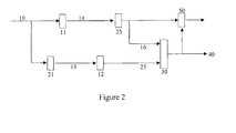
- Figure 2 shows a schematical signal flow diagram in an embodiment for corruption protected delayed lockstep CPUs
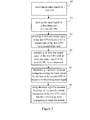
- Figure 3 shows an embodiment of a method for avoiding error propagation in a multi-CPU system.
- system availability describes the fact that - if an error occurs in one of the CPUs - the other CPUs should keep running their respective application.
- duplex systems for a computation cluster also know as lockstep execution of two CPUs.
- Said lockstep execution of CPUs describes the fact that e.g. two CPUs execute the same process delayed by - for instance - two clock cycles to mitigate common cause failures.
- embodiments relate to a prevention or containment of the above-mentioned error propagation - in short - to fault containment.
- embodiments comprise a system and method adapted to delay any output signal of a first CPU - such as typically a signal related to a write transaction of the first CPU - that might cause a propagation of an error while the error is detected.
- this error detection is typically performed on the basis of delayed processing of the same input signal by at least one second CPU, such as in a delayed duplex system, and on the basis of a subsequent comparison of appropriate output signals of the first CPU and the at least one second CPU to generate a corresponding error signal.
- a write transaction of the first lockstep CPU that is ahead of a corresponding write transaction of the second lockstep CPU is delayed.
- this allows then to block the write transaction - for instance by an error blocking unit. Consequently, such error blocking may help to avoid corrupting any resource in the system by the write transaction that has been affected by the error before the error actually could be detected.
- Figure 1 shows a schematical signal flow diagram in a typical implementation of delayed lockstep CPUs.
- an input signal 10 - e.g. a processor command - is fed to a first CPU 11 and processed by the first CPU 11 to output a first output signal 14.
- the input signal 10 is also fed via a first delay unit 21 as a delayed input signal 13 to a second CPU 12 to output a second output signal 25.
- the delayed lockstep configuration of the first CPU 11 and the second CPU 12 means that the first CPU 11 and the second CPU 12 operate in a fixed temporal relation with respect to each other.
- the second CPU 12 is operated by a clock signal, which has the same frequency as the clock signal of the first CPU 11 but is two clock cycles delayed with respect to the latter.
- any common cause at a certain point in time affects the processing of the delayed input signal 13 by the second CPU 12 in the same way as the processing of the input signal 10 by the first CPU 11.
- Such common cause might be an electromagnetic interference (EMI) event, a short drop in the supply voltage for the CPUs or any other event that affects the correct processing of the input signal 10 by the first CPU 11.
- EMI electromagnetic interference
- the second output signal 25 of the second CPU 12 is fed to a comparator unit 30 to be compared with a correspondingly delayed version of the first output signal 14, namely the delayed first output signal 15.
- the first output signal 14 is delayed by a second delay unit 22 to yield the delayed first output signal 15.
- the delayed first output signal 15 of the first CPU 11 will correspond to the second output signal 25 of the second CPU 12.
- the comparator unit 30 will output an error signal 40 which indicates that no error has occurred.
- the delayed first output signal 15 of the first CPU 11 will most likely not correspond to the second output signal 25 of the second CPU 12.
- the comparator unit 30 will then output an error signal 40 which indicates that an error actually has occurred.
- the corrupted first output signal 14 may be related to a write transaction of the first CPU 11 such that the correspondingly corrupted write transaction may cause corruption of the target of this write transaction before the error is actually detected by the comparator unit 30.
- Figure 2 shows a schematical signal flow diagram in an embodiment for corruption protected delayed lockstep CPUs.
- the input signal 10 is fed to the first CPU 11 and processed by the first CPU 11 to output the first output signal 14.
- the input signal 10 is also fed in parallel via the first delay unit 21 as the delayed input signal 13 to the second CPU 12 to output the second output signal 25.
- the second output signal 25 of the second CPU 12 is fed again to the comparator unit 30 to be compared with a correspondingly delayed version of the first output signal 14 in order to detect an error in the processing by the first CPU 11.
- a further second delay unit 23 not only delays the first output signal 14 to yield a further delayed first output signal 16 for the purpose of comparison of the further delayed first output signal 16 with the second output signal 25 by the comparator unit 30. Rather, the further second delay unit 23 applies a delay also to the first output signal 14 for the purpose of delaying the first output signal 14 in general before it may be further processed by subsequent stages.
- the further second delay unit 23 may delay a first output signal 14 related to a write transaction. In this way, there is enough time for the comparator unit 30 to detect an error in the processing by the first CPU 11 by comparing the second output signal 25 of the second CPU 12 with the further delayed first output signal 16 of the first CPU 11 before the corrupted first output signal 14 related to a write transaction may propagate to further stages of the system and corrupt them too.
- the system comprises an error blocking unit 50 adapted to receive the error signal 40 from the comparator unit 30.
- the error signal 40 from the comparator unit 30 may be used to block the further delayed first output signal 16 of the first CPU 11 from propagating into the subsequent parts of the system. As a result, in this case of an error in a write transaction, the integrity of the system may be maintained.
- embodiments may enable delaying write transactions to totally block them or to provide enough time to abort them. This may help multi-core systems to avoid corruption or to restrain it to known memory ranges so that part of the system can keep running.
- the further second delay unit 23 may be implemented in a lot of different ways.
- the further second delay unit 23 may delay all signals from the first CPU 11.
- the further second delay unit 23 may delay only signals related to write transactions.
- the further second delay unit 23 may delay only signals related to a category of write transactions.
- the further second delay unit 23 may delay signals related to write transactions to peripherals and memory attached to a shared internal bus and not delay signals related to write transactions to tightly coupled memories.
- error blocking unit 50 may be implemented in many different ways. In one embodiment, the error blocking unit 50 may actually block a write transaction originating from the first CPU 11 from further propagating through the system.
- the error blocking unit 50 may let a write transaction pass onto the system bus but then send a command to abort the write transaction as soon as an error is detected.
- the error blocking unit 50 may be adapted to modify the address of the write transaction to point to a reserved location or to a "safe" location reserved for that purpose.
- the write transaction may be protected by error detection/correction codes.
- the error blocking unit 50 may be adapted to corrupt the address signature of the write transaction which leads to an error at the target of the write transaction and which - ultimately - aborts the write transaction.
- Figure 3 shows an embodiment of a method for avoiding error propagation in a multi-CPU system.
- step 60 of the method an input signal is received by a first CPU.
- step 61 of the method the input signal is fed by a first delay unit to a second CPU.
- step 62 of the method at least one output signal of the first CPU related to write transactions of the first CPU is delayed by a second delay unit.
- step 63 of the method as shown in Figure 3 at least one output signal of the first CPU is compared by a comparator with at least one output signal of the second CPU.
- step 64 of the method as a result of the above comparison, it is determined if an error occurred during processing the input signal by the first or the second CPU to output a corresponding error signal.
- the error signal is used by an error blocking unit to modify a write transaction of the first CPU such that the error is kept from propagating through the system.
- a first embodiment relates to a system for avoiding error propagation in a multi-CPU system comprising a first CPU and at least one second CPU.
- the at least one second CPU is adapted to operate in delayed lockstep configuration with the first CPU to detect an error by comparing at least one output signal from the first CPU with at least one output signal from the at least one second CPU.
- this system comprises at least one delay unit adapted to delay at least one output signal of the first CPU related to a write transaction of the first CPU to modify at least one write transaction of the first CPU such that the error is kept from propagating through the system.
- the at least one delay unit is adapted to delay all output signals of the first CPU.
- the at least one delay unit is adapted to delay all output signals of the first CPU related to a write transaction of the first CPU.
- the at least one delay unit is adapted to delay at least one output signal of the first CPU related to a predetermined category of write transactions of the first CPU.
- the at least one delay unit is adapted to delay at least one output signal of the first CPU related to write transactions of the first CPU to peripherals and memory attached to a shared internal bus of the first CPU and the at least one second CPU.
- a further embodiment relates to a system comprising a first CPU coupled to receive an input signal, a second CPU and a first delay unit coupled to feed the input signal to the second CPU.
- a second delay unit is coupled to delay at least one output signal of the first CPU related to write transactions of the first CPU.
- said system comprises a comparator unit coupled to compare at least one output signal of the first CPU with at least one output signal of the second CPU to determine if an error occurred during processing the input signal by the first CPU or the second CPU, and output a corresponding error signal.
- said system comprises a protected error blocking unit coupled to use the error signal to modify - under a protection condition - a write transaction of the first CPU such that the error is kept from propagating through the system.
- the error blocking unit is protected in that the system further comprises a further comparator unit coupled to compare the at least one output signal of the first CPU with the at least one output signal of the second CPU.
- the purpose of the further comparator unit is to redundantly determine if an error occurred during processing the input signal by the first CPU or the second CPU, and output a corresponding negated error signal.
- the above system comprises a third comparator unit coupled to verify said protection condition that the error signal and the negated error signal correspondingly agree.
- the protection of the error blocking unit may help to provide a system that is fully compliant with the ISO26262 standard. Specifically, the protection may help to detect and avoid any dangerous situations where the error blocking unit might perform an "unintended" blocking in the absence of a lockstep error.
- the protected error blocking unit is adapted to block the write transaction of the first CPU from being executed.
- the protected error blocking unit is adapted to cause aborting the write transaction of the first CPU as soon as the error is determined.
- the protected error blocking unit is adapted to modify a write transaction address of the write transaction to point to a location reserved for fault containment.
- the protected error blocking unit is adapted to corrupt an address signature of the write transaction if the write transaction is protected by error detection/correction codes leading to an error at the target of the write transaction, and the target of the write transaction aborting the write transaction.
- a still further embodiment relates to a system comprising a processing unit and at least one further processing unit.
- the at least one further processing unit is adapted to process an input signal with a predetermined delay with respect to the processing unit to detect a processing error by comparison of predetermined output signals of the processing unit and the at least one further processing unit.
- this system comprises at least one delay unit adapted to delay at least one output signal of the processing unit to avoid unmodified propagation of at least one output signal of the processing unit through the system if a processing error has been detected.
- the at least one delay unit is adapted to delay at least one output signal of the processing unit related to a write transaction of the processing unit to modify at least one write transaction of the processing unit such that the processing error is kept from propagating through the system.
- system further comprises a protected error blocking unit coupled to use the result of said comparison of the predetermined output signals of the processing unit and the at least one further processing unit to modify - under a protection condition - a write transaction of the processing unit such that the processing error is kept from propagating through the system.
- the error blocking unit is protected in that the system further comprises means to perform a redundant comparison of the predetermined output signals of the processing unit and the at least one further processing unit to redundantly detect if a processing error occurred during processing the input signal by the processing unit or the at least one further processing unit.
- this embodiment comprises means to verify said protection condition that said comparison and said redundant comparison correspondingly agree.
- a delay provided by the at least one delay unit is long enough to enable aborting at least one write transaction of the processing unit.
- a further embodiment relates to a method for avoiding error propagation in a multi-CPU system with a first CPU and at least a second CPU.
- at least one second CPU is operated in delayed lockstep configuration with the first CPU to detect an error in form of at least one different processing result.
- At least one output signal of the first CPU related to a write transaction of the first CPU is delayed to modify at least one write transaction of the first CPU such that the error is kept from propagating through the system.
- delaying comprises delaying all output signals of the first CPU.
- delaying comprises delaying all output signals of the first CPU related to a write transaction of the first CPU.
- delaying comprises delaying at least one output signal of the first CPU related to a predetermined category of write transactions of the first CPU.
- delaying comprises delaying at least one output signal of the first CPU related to write transactions of the first CPU to peripherals and memory attached to a shared internal bus of the first CPU and the at least one second CPU.
- a further embodiment relates to a method for error containment in a system.
- This method comprises the step of processing an input signal by a processing unit and at least one further processing unit to detect an error in form of at least one different processing result.
- at least one output signal of the processing unit is delayed to enable - in case an error has been detected - modifying at least one output signal of the processing unit that would cause propagation of the error through the system.
- delaying comprises delaying at least one output signal of the processing unit related to a write transaction of the processing unit to modify at least one write transaction of the processing unit by an error block unit such that the detected error is kept from propagating through the system.
- modifying the at least one write transaction of the processing unit comprises blocking the write transaction of the first CPU from being executed.
- modifying the at least one write transaction of the processing unit comprises causing the write transaction of the first CPU to abort as soon as the error is detected.
- modifying the at least one write transaction of the processing unit comprises modifying at least one write transaction address of the at least one write transaction to point to a location reserved for fault containment.
- a further embodiment relates to a method for error containment in a system comprising a step of detecting an error by processing an input signal by multiple processing units.
- at least one output signal of a processing unit is delayed to enable - in case an error has been detected - modifying at least one output signal of the processing unit that would cause propagation of the error through the system.
Landscapes
- Engineering & Computer Science (AREA)
- Theoretical Computer Science (AREA)
- Quality & Reliability (AREA)
- Physics & Mathematics (AREA)
- General Engineering & Computer Science (AREA)
- General Physics & Mathematics (AREA)
- Hardware Redundancy (AREA)
Abstract
Description
- The present invention relates generally to a method and system for fault containment in systems for multi-CPU or multi-core microcontrollers, and, in particular, to fault or error containment duplex systems for high integrity microcontrollers in automotive electronic control units (ECUs).
- There is a trend that modem automotive ECUs integrate more and more functionality. On one side, this trend is driven by technology scaling which enables ever increasing levels of integration. Moreover, also the highly cost driven nature of the automotive industry forces developers to reduce the total number of ECUs per vehicle.
- In this context, electronics plays an increasing role in providing advanced driving assistance functions which particularly help to prevent hazards and to reduce the number of fatal injuries.
- The integration of said assistance functions inside an ECU is mainly concentrated around a multi-CPU microcontroller that plays a decisive role by hosting the critical computation and control functions. Such a multi-CPU microcontroller may be regarded as a cluster of computation nodes with defined and encapsulated tasks.
- Under such assumptions - i.e. that a plurality of critical computation and control functions related to various assistance functions are performed by the same multi-CPU microcontroller - failure isolation is a main concern to address in order to ensure that not all assistance functions are affected by a single error. This requirement influences all building blocks of the safety architecture for a system providing fault containment.
- Consequently, embodiments aim at providing a new approach in safely managing errors in order to improve system availability.
- For these or other reasons, there is a need for the present invention.
- A method and system fault containment is provided, substantially as shown in and/or described in connection with at least one of the figures, as set forth more completely in the claims.
According to an aspect, a system is provided for avoiding error propagation in a multi-CPU system comprising: - a first CPU and at least one second CPU, the at least one second CPU adapted to operate in delayed lockstep configuration with the first CPU to detect an error by comparing at least one output signal from the first CPU and with at least one output signal from the at least one second CPU;
- at least one delay unit adapted to delay at least one output signal of the first CPU related to a write transaction of the first CPU to modify at least one write transaction of the first CPU such that the error is kept from propagating through the system.
- a first CPU coupled to receive an input signal;
- a second CPU;
- a first delay unit coupled to feed the input signal to the second CPU;
- a second delay unit coupled to delay at least one output signal of the first CPU related to write transactions of the first CPU;
- a comparator unit coupled to compare at least one output signal of the first CPU with at least one output signal of the second CPU to:
- determine if an error occurred during processing the input signal by the first CPU or the second CPU, and
- output a corresponding error signal;
- a protected error blocking unit coupled to use the error signal to modify - under a protection condition - a write transaction of the first CPU such that the error is kept from propagating through the system.
- a further comparator unit coupled to compare the at least one output signal of the first CPU with the at least one output signal of the second CPU to:
- redundantly determine if an error occurred during processing the input signal by the first CPU or the second CPU, and
- output a corresponding negated error signal;
- a third comparator unit coupled to verify said protection condition that the error signal and the negated error signal correspondingly agree.
- an error at the target of the write transaction, and
- the target of the write transaction aborting the write transaction.
- a processing unit and at least one further processing unit, the latter adapted to process an input signal with a predetermined delay with respect to the processing unit to detect a processing error by comparison of predetermined output signals of the processing unit and the at least one further processing unit; and
- at least one delay unit adapted to delay at least one output signal of the processing unit to avoid unmodified propagation of at least one output signal of the processing unit through the system if a processing error has been detected.
- a protected error blocking unit coupled to use the result of said comparison of the predetermined output signals of the processing unit and the at least one further processing unit to modify - under a protection condition - a write transaction of the processing unit such that the processing error is kept from propagating through the system.
- means to perform a redundant comparison of the predetermined output signals of the processing unit and the at least one further processing unit to redundantly detect if a processing error occurred during processing the input signal by the processing unit or the at least one further processing unit, and
- means to verify said protection condition that said comparison and said redundant comparison correspondingly agree.
- operating at least one second CPU in delayed lockstep configuration with the first CPU to detect an error in form of at least one different processing result; and
- delaying at least one output signal of the first CPU related to a write transaction of the first CPU to modify at least one write transaction of the first CPU such that the error is kept from propagating through the system.
- processing an input signal by a processing unit and at least one further processing unit to detect an error in form of at least one different processing result; and
- delaying at least one output signal of the processing unit to enable - in case an error has been detected - modifying at least one output signal of the processing unit that would cause propagation of the error through the system.
- detecting an error by processing an input signal by multiple processing units; and
- delaying at least one output signal of a processing unit to enable - in case an error has been detected - modifying at least one output signal of the processing unit that would cause propagation of the error through the system.
- Further features and advantages of embodiments will become apparent from the following detailed description made with reference to the accompanying drawings.
- The accompanying drawings are included to provide a further understanding and are incorporated in and constitute a part of this specification. The drawings relate to examples and embodiments and together with the description serve to explain the principles of the invention. Other embodiments and many of the intended advantages of embodiments will be readily appreciated as they become better understood by reference to the following detailed description.
-
Figure 1 shows a schematical signal flow diagram in a typical implementation of delayed lockstep CPUs; -
Figure 2 shows a schematical signal flow diagram in an embodiment for corruption protected delayed lockstep CPUs; and -
Figure 3 shows an embodiment of a method for avoiding error propagation in a multi-CPU system. - In the following Detailed Description, reference is made to the accompanying drawings, which form a part hereof, and in which are shown by way of illustration specific embodiments. It is to be understood that other embodiments may be utilized and structural or other changes may be made without departing from the scope of the present invention. The following detailed description, therefore, is not to be taken in a limiting sense, and the scope of the present invention is defined by the appended claims.
- One key issue regarding multi-CPU or multi-core microcontrollers is system availability. Said system availability describes the fact that - if an error occurs in one of the CPUs - the other CPUs should keep running their respective application.
- This requirement has its parallels with regard to a trend in software architectures that define partitions so that a software error in one partition can be recovered by stopping and restarting this partition only, while the other partitions are isolated from the error.
- For high integrity safety microcontrollers, the state of the art with regard to system integrity is to use duplex systems for a computation cluster, also know as lockstep execution of two CPUs. Said lockstep execution of CPUs describes the fact that e.g. two CPUs execute the same process delayed by - for instance - two clock cycles to mitigate common cause failures.
- Hence, in case of an error in a first lockstep CPU - in the above example - there is also at least a two clock cycle delay to detect the error. This is caused by the fact that the error is typically detected by comparison of a consequently two clock cycles delayed output of a second lockstep CPU with a delayed output of the first lockstep CPU. However, in the meantime until the error is detected, the error - if affecting a write transaction of the first lockstep CPU -may propagate into the rest of the microcontroller system such as an interconnect or a local SRAM.
- Hence, embodiments relate to a prevention or containment of the above-mentioned error propagation - in short - to fault containment.
- Nowadays, automotive ECUs are typically build in a way that a critical error always leads to entering a fail safe mode. However, in such situations, the process of entering the normal mode again is barely defined. In other words, error recovery is just in definition today.
- Since the real complexity of the above-mentioned driving assistance functions is typically reflected in the complexity of the supporting software, there has been no focus in research and development so far on the corresponding microcontroller architecture and its ability to support said error recovery. Accordingly, no circuit is available today to allow to detect error propagation due to the above-mentioned phenomenon in a real application.
- Therefore, embodiments comprise a system and method adapted to delay any output signal of a first CPU - such as typically a signal related to a write transaction of the first CPU - that might cause a propagation of an error while the error is detected.
- As indicated before, this error detection is typically performed on the basis of delayed processing of the same input signal by at least one second CPU, such as in a delayed duplex system, and on the basis of a subsequent comparison of appropriate output signals of the first CPU and the at least one second CPU to generate a corresponding error signal.
- In one embodiment, namely in the context of a duplex system based on a delayed lockstep CPU configuration of two lockstep CPUs, a write transaction of the first lockstep CPU that is ahead of a corresponding write transaction of the second lockstep CPU is delayed.
- In an embodiment, this allows then to block the write transaction - for instance by an error blocking unit. Consequently, such error blocking may help to avoid corrupting any resource in the system by the write transaction that has been affected by the error before the error actually could be detected.
-
Figure 1 shows a schematical signal flow diagram in a typical implementation of delayed lockstep CPUs. In this implementation example of previous delayed lockstep CPUs, an input signal 10 - e.g. a processor command - is fed to afirst CPU 11 and processed by thefirst CPU 11 to output afirst output signal 14. - In parallel, the
input signal 10 is also fed via afirst delay unit 21 as a delayedinput signal 13 to asecond CPU 12 to output asecond output signal 25. As mentioned before, the delayed lockstep configuration of thefirst CPU 11 and thesecond CPU 12 means that thefirst CPU 11 and thesecond CPU 12 operate in a fixed temporal relation with respect to each other. In a typical example, thesecond CPU 12 is operated by a clock signal, which has the same frequency as the clock signal of thefirst CPU 11 but is two clock cycles delayed with respect to the latter. - By delaying the processing of the input signal by the
second CPU 12, the risk may be reduced that any common cause at a certain point in time affects the processing of the delayedinput signal 13 by thesecond CPU 12 in the same way as the processing of theinput signal 10 by thefirst CPU 11. Such common cause might be an electromagnetic interference (EMI) event, a short drop in the supply voltage for the CPUs or any other event that affects the correct processing of theinput signal 10 by thefirst CPU 11. - In order to detect such an error in the processing by the
first CPU 11, thesecond output signal 25 of thesecond CPU 12 is fed to acomparator unit 30 to be compared with a correspondingly delayed version of thefirst output signal 14, namely the delayedfirst output signal 15. In the example inFigure 1 , thefirst output signal 14 is delayed by asecond delay unit 22 to yield the delayedfirst output signal 15. - In case no error occurred during the processing of the
input signal 10 by thefirst CPU 11, the delayedfirst output signal 15 of thefirst CPU 11 will correspond to thesecond output signal 25 of thesecond CPU 12. As a result of the comparison of the delayedfirst output signal 15 with thesecond output signal 25, thecomparator unit 30 will output anerror signal 40 which indicates that no error has occurred. - However, in case an error occurred during the processing of the
input signal 10 by thefirst CPU 11 or during the processing of the delayedinput signal 13 by thesecond CPU 12, the delayedfirst output signal 15 of thefirst CPU 11 will most likely not correspond to thesecond output signal 25 of thesecond CPU 12. As a result of the comparison of the delayedfirst output signal 15 with thesecond output signal 25, thecomparator unit 30 will then output anerror signal 40 which indicates that an error actually has occurred. - Correspondingly, previous multi-CPU systems have been able to detect errors through delayed processing by one or more redundant CPUs and, hence, to avoid that the corrupted
first output signal 14 is used after error detection. However, in meantime until thesecond output signal 25 is available and compared by thecomparator unit 30, the corruptedfirst output signal 14 may propagate into subsequent stages of the system and corrupt any further processing after the detection of the error. - In a typical error case, the corrupted
first output signal 14 may be related to a write transaction of thefirst CPU 11 such that the correspondingly corrupted write transaction may cause corruption of the target of this write transaction before the error is actually detected by thecomparator unit 30. - In contrast to the above,
Figure 2 shows a schematical signal flow diagram in an embodiment for corruption protected delayed lockstep CPUs. In this embodiment - similar to the example inFigure 1 - theinput signal 10 is fed to thefirst CPU 11 and processed by thefirst CPU 11 to output thefirst output signal 14. - Again, the
input signal 10 is also fed in parallel via thefirst delay unit 21 as the delayedinput signal 13 to thesecond CPU 12 to output thesecond output signal 25. Also similar to the example inFigure 1 , thesecond output signal 25 of thesecond CPU 12 is fed again to thecomparator unit 30 to be compared with a correspondingly delayed version of thefirst output signal 14 in order to detect an error in the processing by thefirst CPU 11. - However, in the embodiment for corruption protected delayed lockstep CPUs of
Figure 2 , a furthersecond delay unit 23 not only delays thefirst output signal 14 to yield a further delayedfirst output signal 16 for the purpose of comparison of the further delayedfirst output signal 16 with thesecond output signal 25 by thecomparator unit 30. Rather, the furthersecond delay unit 23 applies a delay also to thefirst output signal 14 for the purpose of delaying thefirst output signal 14 in general before it may be further processed by subsequent stages. - In this regard, the further
second delay unit 23 may delay afirst output signal 14 related to a write transaction. In this way, there is enough time for thecomparator unit 30 to detect an error in the processing by thefirst CPU 11 by comparing thesecond output signal 25 of thesecond CPU 12 with the further delayedfirst output signal 16 of thefirst CPU 11 before the corruptedfirst output signal 14 related to a write transaction may propagate to further stages of the system and corrupt them too. - For this purpose, the system comprises an
error blocking unit 50 adapted to receive theerror signal 40 from thecomparator unit 30. In one embodiment, theerror signal 40 from thecomparator unit 30 may be used to block the further delayedfirst output signal 16 of thefirst CPU 11 from propagating into the subsequent parts of the system. As a result, in this case of an error in a write transaction, the integrity of the system may be maintained. - In other words, embodiments may enable delaying write transactions to totally block them or to provide enough time to abort them. This may help multi-core systems to avoid corruption or to restrain it to known memory ranges so that part of the system can keep running.
- In the following some implementation variants to the embodiment in
Figure 2 are described. For instance, the furthersecond delay unit 23 may be implemented in a lot of different ways. In one embodiment, the furthersecond delay unit 23 may delay all signals from thefirst CPU 11. In another embodiment, the furthersecond delay unit 23 may delay only signals related to write transactions. In a further embodiment, the furthersecond delay unit 23 may delay only signals related to a category of write transactions. For instance, in one embodiment, the furthersecond delay unit 23 may delay signals related to write transactions to peripherals and memory attached to a shared internal bus and not delay signals related to write transactions to tightly coupled memories. - Also the
error blocking unit 50 may be implemented in many different ways. In one embodiment, theerror blocking unit 50 may actually block a write transaction originating from thefirst CPU 11 from further propagating through the system. - In another embodiment, the
error blocking unit 50 may let a write transaction pass onto the system bus but then send a command to abort the write transaction as soon as an error is detected. - In a further embodiment, the
error blocking unit 50 may be adapted to modify the address of the write transaction to point to a reserved location or to a "safe" location reserved for that purpose. - In a still further embodiment, the write transaction may be protected by error detection/correction codes. In this case, the
error blocking unit 50 may be adapted to corrupt the address signature of the write transaction which leads to an error at the target of the write transaction and which - ultimately - aborts the write transaction. -
Figure 3 shows an embodiment of a method for avoiding error propagation in a multi-CPU system. Instep 60 of the method, an input signal is received by a first CPU. - In
step 61 of the method, the input signal is fed by a first delay unit to a second CPU. Instep 62 of the method, at least one output signal of the first CPU related to write transactions of the first CPU is delayed by a second delay unit. - Moreover, in
step 63 of the method as shown inFigure 3 , at least one output signal of the first CPU is compared by a comparator with at least one output signal of the second CPU. - In
step 64 of the method, as a result of the above comparison, it is determined if an error occurred during processing the input signal by the first or the second CPU to output a corresponding error signal. - In a
further step 65 of the method as shown inFigure 3 , the error signal is used by an error blocking unit to modify a write transaction of the first CPU such that the error is kept from propagating through the system. - With respect to the above-described embodiments which relate to the Figures, it is emphasized that said embodiments basically served to increase the comprehensibility. In addition to that, the following further embodiments try to illustrate a more general concept. However, also the following embodiments are not to be taken in a limiting sense. Rather - as expressed before - the scope of the present invention is defined by the appended claims.
- In this regard, a first embodiment relates to a system for avoiding error propagation in a multi-CPU system comprising a first CPU and at least one second CPU. In this system, the at least one second CPU is adapted to operate in delayed lockstep configuration with the first CPU to detect an error by comparing at least one output signal from the first CPU with at least one output signal from the at least one second CPU.
- Furthermore, this system comprises at least one delay unit adapted to delay at least one output signal of the first CPU related to a write transaction of the first CPU to modify at least one write transaction of the first CPU such that the error is kept from propagating through the system.
- In one embodiment, the at least one delay unit is adapted to delay all output signals of the first CPU.
- In another embodiment, the at least one delay unit is adapted to delay all output signals of the first CPU related to a write transaction of the first CPU.
- In still one further embodiment, the at least one delay unit is adapted to delay at least one output signal of the first CPU related to a predetermined category of write transactions of the first CPU.
- According to a further embodiment, the at least one delay unit is adapted to delay at least one output signal of the first CPU related to write transactions of the first CPU to peripherals and memory attached to a shared internal bus of the first CPU and the at least one second CPU.
- A further embodiment relates to a system comprising a first CPU coupled to receive an input signal, a second CPU and a first delay unit coupled to feed the input signal to the second CPU.
- In this system, a second delay unit is coupled to delay at least one output signal of the first CPU related to write transactions of the first CPU. Moreover, said system comprises a comparator unit coupled to compare at least one output signal of the first CPU with at least one output signal of the second CPU to determine if an error occurred during processing the input signal by the first CPU or the second CPU, and output a corresponding error signal.
- Furthermore, said system comprises a protected error blocking unit coupled to use the error signal to modify - under a protection condition - a write transaction of the first CPU such that the error is kept from propagating through the system.
- In an embodiment, the error blocking unit is protected in that the system further comprises a further comparator unit coupled to compare the at least one output signal of the first CPU with the at least one output signal of the second CPU. The purpose of the further comparator unit is to redundantly determine if an error occurred during processing the input signal by the first CPU or the second CPU, and output a corresponding negated error signal.
- Moreover, the above system comprises a third comparator unit coupled to verify said protection condition that the error signal and the negated error signal correspondingly agree.
- In embodiments, the protection of the error blocking unit may help to provide a system that is fully compliant with the ISO26262 standard. Specifically, the protection may help to detect and avoid any dangerous situations where the error blocking unit might perform an "unintended" blocking in the absence of a lockstep error.
- In one embodiment, the protected error blocking unit is adapted to block the write transaction of the first CPU from being executed.
- In another embodiment, the protected error blocking unit is adapted to cause aborting the write transaction of the first CPU as soon as the error is determined.
- In still one further embodiment, the protected error blocking unit is adapted to modify a write transaction address of the write transaction to point to a location reserved for fault containment.
- According to another embodiment, the protected error blocking unit is adapted to corrupt an address signature of the write transaction if the write transaction is protected by error detection/correction codes leading to an error at the target of the write transaction, and the target of the write transaction aborting the write transaction.
- A still further embodiment relates to a system comprising a processing unit and at least one further processing unit. In this system the at least one further processing unit is adapted to process an input signal with a predetermined delay with respect to the processing unit to detect a processing error by comparison of predetermined output signals of the processing unit and the at least one further processing unit.
- Moreover, this system comprises at least one delay unit adapted to delay at least one output signal of the processing unit to avoid unmodified propagation of at least one output signal of the processing unit through the system if a processing error has been detected.
- In an embodiment, the at least one delay unit is adapted to delay at least one output signal of the processing unit related to a write transaction of the processing unit to modify at least one write transaction of the processing unit such that the processing error is kept from propagating through the system.
- In another embodiment, the system further comprises a protected error blocking unit coupled to use the result of said comparison of the predetermined output signals of the processing unit and the at least one further processing unit to modify - under a protection condition - a write transaction of the processing unit such that the processing error is kept from propagating through the system.
- In one embodiment, the error blocking unit is protected in that the system further comprises means to perform a redundant comparison of the predetermined output signals of the processing unit and the at least one further processing unit to redundantly detect if a processing error occurred during processing the input signal by the processing unit or the at least one further processing unit.
- Furthermore, this embodiment comprises means to verify said protection condition that said comparison and said redundant comparison correspondingly agree.
- In one embodiment, a delay provided by the at least one delay unit is long enough to enable aborting at least one write transaction of the processing unit.
- A further embodiment relates to a method for avoiding error propagation in a multi-CPU system with a first CPU and at least a second CPU. In one step of this method, at least one second CPU is operated in delayed lockstep configuration with the first CPU to detect an error in form of at least one different processing result.
- In a further step of the above method, at least one output signal of the first CPU related to a write transaction of the first CPU is delayed to modify at least one write transaction of the first CPU such that the error is kept from propagating through the system.
- In one embodiment, delaying comprises delaying all output signals of the first CPU.
- In another embodiment, delaying comprises delaying all output signals of the first CPU related to a write transaction of the first CPU.
- In a further embodiment, delaying comprises delaying at least one output signal of the first CPU related to a predetermined category of write transactions of the first CPU.
- In a still further embodiment, delaying comprises delaying at least one output signal of the first CPU related to write transactions of the first CPU to peripherals and memory attached to a shared internal bus of the first CPU and the at least one second CPU.
- A further embodiment relates to a method for error containment in a system. This method comprises the step of processing an input signal by a processing unit and at least one further processing unit to detect an error in form of at least one different processing result. In a further step of this method, at least one output signal of the processing unit is delayed to enable - in case an error has been detected - modifying at least one output signal of the processing unit that would cause propagation of the error through the system.
- In an embodiment, delaying comprises delaying at least one output signal of the processing unit related to a write transaction of the processing unit to modify at least one write transaction of the processing unit by an error block unit such that the detected error is kept from propagating through the system.
- In one embodiment, modifying the at least one write transaction of the processing unit comprises blocking the write transaction of the first CPU from being executed.
- In another embodiment, modifying the at least one write transaction of the processing unit comprises causing the write transaction of the first CPU to abort as soon as the error is detected.
- In a still further embodiment, modifying the at least one write transaction of the processing unit comprises modifying at least one write transaction address of the at least one write transaction to point to a location reserved for fault containment.
- A further embodiment relates to a method for error containment in a system comprising a step of detecting an error by processing an input signal by multiple processing units. In a further step, at least one output signal of a processing unit is delayed to enable - in case an error has been detected - modifying at least one output signal of the processing unit that would cause propagation of the error through the system.
- Although specific embodiments have been illustrated and described herein, it will be appreciated by those of ordinary skill in the art that a variety of alternate and/or equivalent implementations may be substituted for the specific embodiments shown and described without departing from the scope of the present invention. This application is intended to cover any adaptations or variations of the specific embodiments discussed herein. Therefore, it is intended that this invention be limited only by the claims and the equivalents thereof.
Advantageously, the at least one delay unit is adapted to delay all output signals of the first CPU related to a write transaction of the first CPU.
Advantageously, the at least one delay unit is adapted to delay at least one output signal of the first CPU related to a predetermined category of write transactions of the first CPU.
Advantageously, the at least one delay unit is adapted to delay at least one output signal of the first CPU related to write transactions of the first CPU to peripherals and memory attached to a shared internal bus of the first CPU and the at least one second CPU.
According to an aspect, a system comprises:
Advantageously, the protected error blocking unit is adapted to cause aborting the write transaction of the first CPU as soon as the error is determined.
Advantageously, the protected error blocking unit is adapted to modify a write transaction address of the write transaction to point to a location reserved for fault containment.
Advantageously, the protected error blocking unit is adapted to corrupt an address signature of the write transaction if the write transaction is protected by error detection/correction codes, leading to:
Advantageously, the system further comprises:
According to an aspect, a method is provided for avoiding error propagation in a multi-CPU system with a first CPU and at least a second CPU, the method comprising:
Advantageously, delaying comprises delaying all output signals of the first CPU related to a write transaction of the first CPU.
Advantageously, delaying comprises delaying at least one output signal of the first CPU related to a predetermined category of write transactions of the first CPU.
Advantageously, delaying comprises delaying at least one output signal of the first CPU related to write transactions of the first CPU to peripherals and memory attached to a shared internal bus of the first CPU and the at least one second CPU.
According to an aspect, a method for error containment in a system comprises:
Advantageously, modifying the at least one write transaction of the processing unit comprises blocking the write transaction of the first CPU from being executed.
Advantageously, modifying the at least one write transaction of the processing unit comprises causing the write transaction of the first CPU to abort as soon as the error is detected.
Advantageously, modifying the at least one write transaction of the processing unit comprises modifying at least one write transaction address of the at least one write transaction to point to a location reserved for fault containment.
According to an aspect, a method for error containment in a system comprises:
Claims (15)
- A system for avoiding error propagation in a multi-CPU system comprising:a first CPU and at least one second CPU, the at least one second CPU adapted to operate in delayed lockstep configuration with the first CPU to detect an error by comparing at least one output signal from the first CPU and with at least one output signal from the at least one second CPU;at least one delay unit adapted to delay at least one output signal of the first CPU related to a write transaction of the first CPU to modify at least one write transaction of the first CPU such that the error is kept from propagating through the system.
- The system of claim 1, wherein the at least one delay unit is adapted to delay all output signals of the first CPU.
- The system of claim 1, wherein the at least one delay unit is adapted to delay all output signals of the first CPU related to a write transaction of the first CPU.
- The system of claim 1, wherein the at least one delay unit is adapted to delay at least one output signal of the first CPU related to a predetermined category of write transactions of the first CPU.
- The system of claim 1, wherein the at least one delay unit is adapted to delay at least one output signal of the first CPU related to write transactions of the first CPU to peripherals and memory attached to a shared internal bus of the first CPU and the at least one second CPU.
- A system comprising:a first CPU coupled to receive an input signal;a second CPU;a first delay unit coupled to feed the input signal to the second CPU;a second delay unit coupled to delay at least one output signal of the first CPU related to write transactions of the first CPU;a comparator unit coupled to compare at least one output signal of the first CPU with at least one output signal of the second CPU to:determine if an error occurred during processing the input signal by the first CPU or the second CPU, andoutput a corresponding error signal;a protected error blocking unit coupled to use the error signal to modify - under a protection condition - a write transaction of the first CPU such that the error is kept from propagating through the system.
- The system of claim 6, wherein the error blocking unit is protected in that the system further comprises:a further comparator unit coupled to compare the at least one output signal of the first CPU with the at least one output signal of the second CPU to:redundantly determine if an error occurred during processing the input signal by the first CPU or the second CPU, andoutput a corresponding negated error signal;a third comparator unit coupled to verify said protection condition that the error signal and the negated error signal correspondingly agree.
- The system of claim 6, wherein the protected error blocking unit is adapted to block the write transaction of the first CPU from being executed.
- The system of claim 6, wherein the protected error blocking unit is adapted to cause aborting the write transaction of the first CPU as soon as the error is determined.
- The system of claim 6, wherein the protected error blocking unit is adapted to modify a write transaction address of the write transaction to point to a location reserved for fault containment.
- The system of claim 6, wherein the protected error blocking unit is adapted to corrupt an address signature of the write transaction if the write transaction is protected by error detection/correction codes, leading to:an error at the target of the write transaction, andthe target of the write transaction aborting the write transaction.
- A system comprising:a processing unit and at least one further processing unit, the latter adapted to process an input signal with a predetermined delay with respect to the processing unit to detect a processing error by comparison of predetermined output signals of the processing unit and the at least one further processing unit; andat least one delay unit adapted to delay at least one output signal of the processing unit to avoid unmodified propagation of at least one output signal of the processing unit through the system if a processing error has been detected.
- A method for avoiding error propagation in a multi-CPU system with a first CPU and at least a second CPU, the method comprising:operating at least one second CPU in delayed lockstep configuration with the first CPU to detect an error in form of at least one different processing result; anddelaying at least one output signal of the first CPU related to a write transaction of the first CPU to modify at least one write transaction of the first CPU such that the error is kept from propagating through the system.
- The method of claim 13, wherein delaying comprises delaying all output signals of the first CPU.
- The method of claim 13, wherein delaying comprises delaying all output signals of the first CPU related to a write transaction of the first CPU.
Applications Claiming Priority (1)
| Application Number | Priority Date | Filing Date | Title |
|---|---|---|---|
| US13/417,382 US8819485B2 (en) | 2012-03-12 | 2012-03-12 | Method and system for fault containment |
Publications (2)
| Publication Number | Publication Date |
|---|---|
| EP2639699A1 true EP2639699A1 (en) | 2013-09-18 |
| EP2639699B1 EP2639699B1 (en) | 2015-08-05 |
Family
ID=47915390
Family Applications (1)
| Application Number | Title | Priority Date | Filing Date |
|---|---|---|---|
| EP13001212.3A Active EP2639699B1 (en) | 2012-03-12 | 2013-03-11 | Method and system for fault containment |
Country Status (3)
| Country | Link |
|---|---|
| US (2) | US8819485B2 (en) |
| EP (1) | EP2639699B1 (en) |
| CN (1) | CN103309760A (en) |
Families Citing this family (14)
| Publication number | Priority date | Publication date | Assignee | Title |
|---|---|---|---|---|
| US8819485B2 (en) * | 2012-03-12 | 2014-08-26 | Infineon Technologies Ag | Method and system for fault containment |
| KR20140134376A (en) * | 2013-05-14 | 2014-11-24 | 한국전자통신연구원 | Processor capable of fault detection and method of detecting fault of processor core using the same |
| CN103544087B (en) * | 2013-10-30 | 2015-10-28 | 中国航空工业集团公司第六三一研究所 | A kind of processor bus method for supervising of lock-step and computing machine |
| US10761925B2 (en) * | 2015-03-24 | 2020-09-01 | Nxp Usa, Inc. | Multi-channel network-on-a-chip |
| US10002056B2 (en) * | 2015-09-15 | 2018-06-19 | Texas Instruments Incorporated | Integrated circuit chip with cores asymmetrically oriented with respect to each other |
| US10331532B2 (en) * | 2017-01-19 | 2019-06-25 | Qualcomm Incorporated | Periodic non-intrusive diagnosis of lockstep systems |
| US10303566B2 (en) * | 2017-07-10 | 2019-05-28 | Arm Limited | Apparatus and method for checking output data during redundant execution of instructions |
| DE102018120328A1 (en) * | 2017-08-24 | 2019-02-28 | Infineon Technologies Ag | Safety device with extended reliability |
| US10802932B2 (en) * | 2017-12-04 | 2020-10-13 | Nxp Usa, Inc. | Data processing system having lockstep operation |
| US10761561B2 (en) * | 2018-05-25 | 2020-09-01 | Arm Limited | Error checking for primary signal transmitted between first and second clock domains |
| US11424621B2 (en) | 2020-01-28 | 2022-08-23 | Qualcomm Incorporated | Configurable redundant systems for safety critical applications |
| US11636227B2 (en) * | 2020-11-16 | 2023-04-25 | Nxp B.V. | Protection against fault attacks by duplication |
| US11687428B2 (en) | 2021-01-20 | 2023-06-27 | Stmicroelectronics International N.V. | Glitch suppression apparatus and method |
| US11928475B2 (en) * | 2021-11-05 | 2024-03-12 | Ceremorphic, Inc. | Fast recovery for dual core lock step |
Citations (4)
| Publication number | Priority date | Publication date | Assignee | Title |
|---|---|---|---|---|
| GB2317032A (en) * | 1996-09-07 | 1998-03-11 | Motorola Gmbh | Microprocessor fail-safe system |
| US20030229836A1 (en) * | 2002-02-22 | 2003-12-11 | Seiko Epson Corporation | Integrated circuit |
| US20070283061A1 (en) * | 2004-08-06 | 2007-12-06 | Robert Bosch Gmbh | Method for Delaying Accesses to Date and/or Instructions of a Two-Computer System, and Corresponding Delay Unit |
| US20080244305A1 (en) * | 2007-03-30 | 2008-10-02 | Texas Instruments Deutschland, Gmbh | Delayed lock-step cpu compare |
Family Cites Families (12)
| Publication number | Priority date | Publication date | Assignee | Title |
|---|---|---|---|---|
| US4635223A (en) | 1983-05-16 | 1987-01-06 | Motorola, Inc. | Fail safe protection circuitry for a commerical microprocessor in encryption equipment |
| JPH0721769B2 (en) | 1988-08-12 | 1995-03-08 | 日本電気株式会社 | Function monitoring method by redundant configuration of microprocessor |
| CN1168004C (en) * | 1989-05-17 | 2004-09-22 | 国际商业机器公司 | Apparatus for providing a fault-tolerant environment and architecture in a data processing system |
| JPH05128080A (en) | 1991-10-14 | 1993-05-25 | Mitsubishi Electric Corp | Information processing equipment |
| US5748873A (en) * | 1992-09-17 | 1998-05-05 | Hitachi,Ltd. | Fault recovering system provided in highly reliable computer system having duplicated processors |
| GB2340627B (en) * | 1998-08-13 | 2000-10-04 | Plessey Telecomm | Data processing system |
| US6615366B1 (en) * | 1999-12-21 | 2003-09-02 | Intel Corporation | Microprocessor with dual execution core operable in high reliability mode |
| US20090177866A1 (en) * | 2008-01-08 | 2009-07-09 | Choate Michael L | System and method for functionally redundant computing system having a configurable delay between logically synchronized processors |
| US8019861B2 (en) * | 2009-01-29 | 2011-09-13 | Vmware, Inc. | Speculative virtual machine resource scheduling |
| US8275977B2 (en) * | 2009-04-08 | 2012-09-25 | Freescale Semiconductor, Inc. | Debug signaling in a multiple processor data processing system |
| US9146835B2 (en) * | 2012-01-05 | 2015-09-29 | International Business Machines Corporation | Methods and systems with delayed execution of multiple processors |
| US8819485B2 (en) * | 2012-03-12 | 2014-08-26 | Infineon Technologies Ag | Method and system for fault containment |
-
2012
- 2012-03-12 US US13/417,382 patent/US8819485B2/en active Active
-
2013
- 2013-03-11 EP EP13001212.3A patent/EP2639699B1/en active Active
- 2013-03-12 CN CN2013100775886A patent/CN103309760A/en active Pending
-
2014
- 2014-07-22 US US14/337,699 patent/US9417946B2/en active Active
Patent Citations (4)
| Publication number | Priority date | Publication date | Assignee | Title |
|---|---|---|---|---|
| GB2317032A (en) * | 1996-09-07 | 1998-03-11 | Motorola Gmbh | Microprocessor fail-safe system |
| US20030229836A1 (en) * | 2002-02-22 | 2003-12-11 | Seiko Epson Corporation | Integrated circuit |
| US20070283061A1 (en) * | 2004-08-06 | 2007-12-06 | Robert Bosch Gmbh | Method for Delaying Accesses to Date and/or Instructions of a Two-Computer System, and Corresponding Delay Unit |
| US20080244305A1 (en) * | 2007-03-30 | 2008-10-02 | Texas Instruments Deutschland, Gmbh | Delayed lock-step cpu compare |
Also Published As
| Publication number | Publication date |
|---|---|
| US9417946B2 (en) | 2016-08-16 |
| EP2639699B1 (en) | 2015-08-05 |
| US8819485B2 (en) | 2014-08-26 |
| US20140337670A1 (en) | 2014-11-13 |
| US20130238945A1 (en) | 2013-09-12 |
| CN103309760A (en) | 2013-09-18 |
Similar Documents
| Publication | Publication Date | Title |
|---|---|---|
| EP2639699B1 (en) | Method and system for fault containment | |
| CN101243407B (en) | Method and apparatus for controlling a computer system | |
| CN103262045B (en) | Microprocessor system having fault-tolerant architecture | |
| US10576990B2 (en) | Method and device for handling safety critical errors | |
| US9058419B2 (en) | System and method for verifying the integrity of a safety-critical vehicle control system | |
| US20080163035A1 (en) | Method for Data Distribution and Data Distribution Unit in a Multiprocessor System | |
| US11392385B2 (en) | System and method for auto-recovery in lockstep processors | |
| EP2824573B1 (en) | Microcomputer test | |
| CN102640119B (en) | Method for operating a processor | |
| US8954794B2 (en) | Method and system for detection of latent faults in microcontrollers | |
| CN104346306B (en) | The system and method for high integrality dma operation | |
| JP2012068788A (en) | Information processing device and failure detection method | |
| Brewerton et al. | Demonstration of automotive steering column lock using multicore autosar® operating system | |
| CN112424753B (en) | Multi-core systems | |
| KR101576848B1 (en) | Error signal handling unit, device and method for outputting an error condition signal | |
| WO2018003560A1 (en) | Electronic control device | |
| JP2011095837A (en) | Fail-safe system | |
| CN107423029B (en) | Calculation unit | |
| EP3367242B1 (en) | Method of error detection in a microcontroller unit | |
| CN114816863A (en) | Burr suppression device and method | |
| KR101923778B1 (en) | Method thereof and apparatus for high performance computing using dual modular redundancy and error prediction | |
| Schneider et al. | Basic single-microcontroller monitoring concept for safety critical systems | |
| JP5287198B2 (en) | Information processing device | |
| JP2009093393A (en) | Data processing device, and self-diagnosis method for data processing device | |
| Niimi et al. | Virtualization Technology and Using Virtual CPU in the Context of ISO26262: The E-Gas Case Study |
Legal Events
| Date | Code | Title | Description |
|---|---|---|---|
| PUAI | Public reference made under article 153(3) epc to a published international application that has entered the european phase |
Free format text: ORIGINAL CODE: 0009012 |
|
| AK | Designated contracting states |
Kind code of ref document: A1 Designated state(s): AL AT BE BG CH CY CZ DE DK EE ES FI FR GB GR HR HU IE IS IT LI LT LU LV MC MK MT NL NO PL PT RO RS SE SI SK SM TR |
|
| AX | Request for extension of the european patent |
Extension state: BA ME |
|
| 17P | Request for examination filed |
Effective date: 20140107 |
|
| RBV | Designated contracting states (corrected) |
Designated state(s): AL AT BE BG CH CY CZ DE DK EE ES FI FR GB GR HR HU IE IS IT LI LT LU LV MC MK MT NL NO PL PT RO RS SE SI SK SM TR |
|
| 17Q | First examination report despatched |
Effective date: 20140407 |
|
| GRAP | Despatch of communication of intention to grant a patent |
Free format text: ORIGINAL CODE: EPIDOSNIGR1 |
|
| RIC1 | Information provided on ipc code assigned before grant |
Ipc: G06F 11/16 20060101AFI20150219BHEP Ipc: G06F 11/07 20060101ALI20150219BHEP |
|
| INTG | Intention to grant announced |
Effective date: 20150316 |
|
| GRAS | Grant fee paid |
Free format text: ORIGINAL CODE: EPIDOSNIGR3 |
|
| GRAA | (expected) grant |
Free format text: ORIGINAL CODE: 0009210 |
|
| AK | Designated contracting states |
Kind code of ref document: B1 Designated state(s): AL AT BE BG CH CY CZ DE DK EE ES FI FR GB GR HR HU IE IS IT LI LT LU LV MC MK MT NL NO PL PT RO RS SE SI SK SM TR |
|
| REG | Reference to a national code |
Ref country code: GB Ref legal event code: FG4D |
|
| REG | Reference to a national code |
Ref country code: CH Ref legal event code: EP |
|
| REG | Reference to a national code |
Ref country code: AT Ref legal event code: REF Ref document number: 741065 Country of ref document: AT Kind code of ref document: T Effective date: 20150815 |
|
| REG | Reference to a national code |
Ref country code: IE Ref legal event code: FG4D |
|
| REG | Reference to a national code |
Ref country code: DE Ref legal event code: R096 Ref document number: 602013002465 Country of ref document: DE |
|
| REG | Reference to a national code |
Ref country code: AT Ref legal event code: MK05 Ref document number: 741065 Country of ref document: AT Kind code of ref document: T Effective date: 20150805 |
|
| REG | Reference to a national code |
Ref country code: LT Ref legal event code: MG4D |
|
| REG | Reference to a national code |
Ref country code: NL Ref legal event code: MP Effective date: 20150805 |
|
| PG25 | Lapsed in a contracting state [announced via postgrant information from national office to epo] |
Ref country code: NO Free format text: LAPSE BECAUSE OF FAILURE TO SUBMIT A TRANSLATION OF THE DESCRIPTION OR TO PAY THE FEE WITHIN THE PRESCRIBED TIME-LIMIT Effective date: 20151105 Ref country code: FI Free format text: LAPSE BECAUSE OF FAILURE TO SUBMIT A TRANSLATION OF THE DESCRIPTION OR TO PAY THE FEE WITHIN THE PRESCRIBED TIME-LIMIT Effective date: 20150805 Ref country code: LV Free format text: LAPSE BECAUSE OF FAILURE TO SUBMIT A TRANSLATION OF THE DESCRIPTION OR TO PAY THE FEE WITHIN THE PRESCRIBED TIME-LIMIT Effective date: 20150805 Ref country code: GR Free format text: LAPSE BECAUSE OF FAILURE TO SUBMIT A TRANSLATION OF THE DESCRIPTION OR TO PAY THE FEE WITHIN THE PRESCRIBED TIME-LIMIT Effective date: 20151106 Ref country code: LT Free format text: LAPSE BECAUSE OF FAILURE TO SUBMIT A TRANSLATION OF THE DESCRIPTION OR TO PAY THE FEE WITHIN THE PRESCRIBED TIME-LIMIT Effective date: 20150805 |
|
| PG25 | Lapsed in a contracting state [announced via postgrant information from national office to epo] |
Ref country code: SE Free format text: LAPSE BECAUSE OF FAILURE TO SUBMIT A TRANSLATION OF THE DESCRIPTION OR TO PAY THE FEE WITHIN THE PRESCRIBED TIME-LIMIT Effective date: 20150805 Ref country code: AT Free format text: LAPSE BECAUSE OF FAILURE TO SUBMIT A TRANSLATION OF THE DESCRIPTION OR TO PAY THE FEE WITHIN THE PRESCRIBED TIME-LIMIT Effective date: 20150805 Ref country code: IS Free format text: LAPSE BECAUSE OF FAILURE TO SUBMIT A TRANSLATION OF THE DESCRIPTION OR TO PAY THE FEE WITHIN THE PRESCRIBED TIME-LIMIT Effective date: 20151205 Ref country code: ES Free format text: LAPSE BECAUSE OF FAILURE TO SUBMIT A TRANSLATION OF THE DESCRIPTION OR TO PAY THE FEE WITHIN THE PRESCRIBED TIME-LIMIT Effective date: 20150805 Ref country code: HR Free format text: LAPSE BECAUSE OF FAILURE TO SUBMIT A TRANSLATION OF THE DESCRIPTION OR TO PAY THE FEE WITHIN THE PRESCRIBED TIME-LIMIT Effective date: 20150805 Ref country code: PT Free format text: LAPSE BECAUSE OF FAILURE TO SUBMIT A TRANSLATION OF THE DESCRIPTION OR TO PAY THE FEE WITHIN THE PRESCRIBED TIME-LIMIT Effective date: 20151207 Ref country code: PL Free format text: LAPSE BECAUSE OF FAILURE TO SUBMIT A TRANSLATION OF THE DESCRIPTION OR TO PAY THE FEE WITHIN THE PRESCRIBED TIME-LIMIT Effective date: 20150805 Ref country code: RS Free format text: LAPSE BECAUSE OF FAILURE TO SUBMIT A TRANSLATION OF THE DESCRIPTION OR TO PAY THE FEE WITHIN THE PRESCRIBED TIME-LIMIT Effective date: 20150805 |
|
| REG | Reference to a national code |
Ref country code: FR Ref legal event code: PLFP Year of fee payment: 4 |
|
| PG25 | Lapsed in a contracting state [announced via postgrant information from national office to epo] |
Ref country code: NL Free format text: LAPSE BECAUSE OF FAILURE TO SUBMIT A TRANSLATION OF THE DESCRIPTION OR TO PAY THE FEE WITHIN THE PRESCRIBED TIME-LIMIT Effective date: 20150805 |
|
| PG25 | Lapsed in a contracting state [announced via postgrant information from national office to epo] |
Ref country code: EE Free format text: LAPSE BECAUSE OF FAILURE TO SUBMIT A TRANSLATION OF THE DESCRIPTION OR TO PAY THE FEE WITHIN THE PRESCRIBED TIME-LIMIT Effective date: 20150805 Ref country code: DK Free format text: LAPSE BECAUSE OF FAILURE TO SUBMIT A TRANSLATION OF THE DESCRIPTION OR TO PAY THE FEE WITHIN THE PRESCRIBED TIME-LIMIT Effective date: 20150805 Ref country code: IT Free format text: LAPSE BECAUSE OF FAILURE TO SUBMIT A TRANSLATION OF THE DESCRIPTION OR TO PAY THE FEE WITHIN THE PRESCRIBED TIME-LIMIT Effective date: 20150805 Ref country code: CZ Free format text: LAPSE BECAUSE OF FAILURE TO SUBMIT A TRANSLATION OF THE DESCRIPTION OR TO PAY THE FEE WITHIN THE PRESCRIBED TIME-LIMIT Effective date: 20150805 Ref country code: SK Free format text: LAPSE BECAUSE OF FAILURE TO SUBMIT A TRANSLATION OF THE DESCRIPTION OR TO PAY THE FEE WITHIN THE PRESCRIBED TIME-LIMIT Effective date: 20150805 |
|
| REG | Reference to a national code |
Ref country code: DE Ref legal event code: R097 Ref document number: 602013002465 Country of ref document: DE |
|
| PG25 | Lapsed in a contracting state [announced via postgrant information from national office to epo] |
Ref country code: RO Free format text: LAPSE BECAUSE OF FAILURE TO SUBMIT A TRANSLATION OF THE DESCRIPTION OR TO PAY THE FEE WITHIN THE PRESCRIBED TIME-LIMIT Effective date: 20150805 |
|
| PLBE | No opposition filed within time limit |
Free format text: ORIGINAL CODE: 0009261 |
|
| STAA | Information on the status of an ep patent application or granted ep patent |
Free format text: STATUS: NO OPPOSITION FILED WITHIN TIME LIMIT |
|
| 26N | No opposition filed |
Effective date: 20160509 |
|
| PG25 | Lapsed in a contracting state [announced via postgrant information from national office to epo] |
Ref country code: BE Free format text: LAPSE BECAUSE OF NON-PAYMENT OF DUE FEES Effective date: 20160331 Ref country code: SI Free format text: LAPSE BECAUSE OF FAILURE TO SUBMIT A TRANSLATION OF THE DESCRIPTION OR TO PAY THE FEE WITHIN THE PRESCRIBED TIME-LIMIT Effective date: 20150805 |
|
| PG25 | Lapsed in a contracting state [announced via postgrant information from national office to epo] |
Ref country code: LU Free format text: LAPSE BECAUSE OF FAILURE TO SUBMIT A TRANSLATION OF THE DESCRIPTION OR TO PAY THE FEE WITHIN THE PRESCRIBED TIME-LIMIT Effective date: 20160311 Ref country code: MC Free format text: LAPSE BECAUSE OF FAILURE TO SUBMIT A TRANSLATION OF THE DESCRIPTION OR TO PAY THE FEE WITHIN THE PRESCRIBED TIME-LIMIT Effective date: 20150805 |
|
| REG | Reference to a national code |
Ref country code: CH Ref legal event code: PL |
|
| REG | Reference to a national code |
Ref country code: IE Ref legal event code: MM4A |
|
| PG25 | Lapsed in a contracting state [announced via postgrant information from national office to epo] |
Ref country code: BE Free format text: LAPSE BECAUSE OF FAILURE TO SUBMIT A TRANSLATION OF THE DESCRIPTION OR TO PAY THE FEE WITHIN THE PRESCRIBED TIME-LIMIT Effective date: 20150805 |
|
| PG25 | Lapsed in a contracting state [announced via postgrant information from national office to epo] |
Ref country code: CH Free format text: LAPSE BECAUSE OF NON-PAYMENT OF DUE FEES Effective date: 20160331 Ref country code: LI Free format text: LAPSE BECAUSE OF NON-PAYMENT OF DUE FEES Effective date: 20160331 Ref country code: IE Free format text: LAPSE BECAUSE OF NON-PAYMENT OF DUE FEES Effective date: 20160311 |
|
| REG | Reference to a national code |
Ref country code: FR Ref legal event code: PLFP Year of fee payment: 5 |
|
| PG25 | Lapsed in a contracting state [announced via postgrant information from national office to epo] |
Ref country code: MT Free format text: LAPSE BECAUSE OF FAILURE TO SUBMIT A TRANSLATION OF THE DESCRIPTION OR TO PAY THE FEE WITHIN THE PRESCRIBED TIME-LIMIT Effective date: 20150805 |
|
| GBPC | Gb: european patent ceased through non-payment of renewal fee |
Effective date: 20170311 |
|
| PG25 | Lapsed in a contracting state [announced via postgrant information from national office to epo] |
Ref country code: GB Free format text: LAPSE BECAUSE OF NON-PAYMENT OF DUE FEES Effective date: 20170311 |
|
| REG | Reference to a national code |
Ref country code: FR Ref legal event code: PLFP Year of fee payment: 6 |
|
| PG25 | Lapsed in a contracting state [announced via postgrant information from national office to epo] |
Ref country code: HU Free format text: LAPSE BECAUSE OF FAILURE TO SUBMIT A TRANSLATION OF THE DESCRIPTION OR TO PAY THE FEE WITHIN THE PRESCRIBED TIME-LIMIT; INVALID AB INITIO Effective date: 20130311 Ref country code: CY Free format text: LAPSE BECAUSE OF FAILURE TO SUBMIT A TRANSLATION OF THE DESCRIPTION OR TO PAY THE FEE WITHIN THE PRESCRIBED TIME-LIMIT Effective date: 20150805 Ref country code: SM Free format text: LAPSE BECAUSE OF FAILURE TO SUBMIT A TRANSLATION OF THE DESCRIPTION OR TO PAY THE FEE WITHIN THE PRESCRIBED TIME-LIMIT Effective date: 20150805 |
|
| PG25 | Lapsed in a contracting state [announced via postgrant information from national office to epo] |
Ref country code: MT Free format text: LAPSE BECAUSE OF FAILURE TO SUBMIT A TRANSLATION OF THE DESCRIPTION OR TO PAY THE FEE WITHIN THE PRESCRIBED TIME-LIMIT Effective date: 20160331 Ref country code: TR Free format text: LAPSE BECAUSE OF FAILURE TO SUBMIT A TRANSLATION OF THE DESCRIPTION OR TO PAY THE FEE WITHIN THE PRESCRIBED TIME-LIMIT Effective date: 20150805 Ref country code: MK Free format text: LAPSE BECAUSE OF FAILURE TO SUBMIT A TRANSLATION OF THE DESCRIPTION OR TO PAY THE FEE WITHIN THE PRESCRIBED TIME-LIMIT Effective date: 20150805 |
|
| PG25 | Lapsed in a contracting state [announced via postgrant information from national office to epo] |
Ref country code: BG Free format text: LAPSE BECAUSE OF FAILURE TO SUBMIT A TRANSLATION OF THE DESCRIPTION OR TO PAY THE FEE WITHIN THE PRESCRIBED TIME-LIMIT Effective date: 20150805 |
|
| PG25 | Lapsed in a contracting state [announced via postgrant information from national office to epo] |
Ref country code: AL Free format text: LAPSE BECAUSE OF FAILURE TO SUBMIT A TRANSLATION OF THE DESCRIPTION OR TO PAY THE FEE WITHIN THE PRESCRIBED TIME-LIMIT Effective date: 20150805 |
|
| PGFP | Annual fee paid to national office [announced via postgrant information from national office to epo] |
Ref country code: FR Payment date: 20230327 Year of fee payment: 11 |
|
| P01 | Opt-out of the competence of the unified patent court (upc) registered |
Effective date: 20230528 |
|
| PG25 | Lapsed in a contracting state [announced via postgrant information from national office to epo] |
Ref country code: FR Free format text: LAPSE BECAUSE OF NON-PAYMENT OF DUE FEES Effective date: 20240331 |
|
| PG25 | Lapsed in a contracting state [announced via postgrant information from national office to epo] |
Ref country code: FR Free format text: LAPSE BECAUSE OF NON-PAYMENT OF DUE FEES Effective date: 20240331 |
|
| PGFP | Annual fee paid to national office [announced via postgrant information from national office to epo] |
Ref country code: DE Payment date: 20250521 Year of fee payment: 13 |