EP2639593A1 - Magntic sensor manufacturing - Google Patents
Magntic sensor manufacturing Download PDFInfo
- Publication number
- EP2639593A1 EP2639593A1 EP13159039.0A EP13159039A EP2639593A1 EP 2639593 A1 EP2639593 A1 EP 2639593A1 EP 13159039 A EP13159039 A EP 13159039A EP 2639593 A1 EP2639593 A1 EP 2639593A1
- Authority
- EP
- European Patent Office
- Prior art keywords
- layer
- annealing
- situ
- thermal annealing
- depositing
- Prior art date
- Legal status (The legal status is an assumption and is not a legal conclusion. Google has not performed a legal analysis and makes no representation as to the accuracy of the status listed.)
- Granted
Links
- 238000004519 manufacturing process Methods 0.000 title claims description 19
- 238000011065 in-situ storage Methods 0.000 claims abstract description 99
- 230000004888 barrier function Effects 0.000 claims abstract description 69
- 238000004151 rapid thermal annealing Methods 0.000 claims abstract description 46
- 238000000137 annealing Methods 0.000 claims description 88
- 238000000151 deposition Methods 0.000 claims description 66
- 238000000034 method Methods 0.000 claims description 50
- 125000006850 spacer group Chemical group 0.000 claims description 24
- 238000001816 cooling Methods 0.000 claims description 19
- 238000005530 etching Methods 0.000 claims description 13
- 230000005291 magnetic effect Effects 0.000 abstract description 20
- 230000008569 process Effects 0.000 description 24
- 230000005290 antiferromagnetic effect Effects 0.000 description 23
- 239000000463 material Substances 0.000 description 19
- 230000008021 deposition Effects 0.000 description 15
- 235000012431 wafers Nutrition 0.000 description 12
- 230000006872 improvement Effects 0.000 description 5
- 238000010586 diagram Methods 0.000 description 4
- 238000011066 ex-situ storage Methods 0.000 description 4
- 238000010884 ion-beam technique Methods 0.000 description 4
- 230000005641 tunneling Effects 0.000 description 3
- 230000008859 change Effects 0.000 description 2
- 239000003989 dielectric material Substances 0.000 description 2
- 238000009792 diffusion process Methods 0.000 description 2
- 238000010438 heat treatment Methods 0.000 description 2
- 238000009413 insulation Methods 0.000 description 2
- 230000007246 mechanism Effects 0.000 description 2
- 238000001020 plasma etching Methods 0.000 description 2
- 238000001953 recrystallisation Methods 0.000 description 2
- 239000010409 thin film Substances 0.000 description 2
- 229910003321 CoFe Inorganic materials 0.000 description 1
- 238000010521 absorption reaction Methods 0.000 description 1
- 238000013500 data storage Methods 0.000 description 1
- 230000003111 delayed effect Effects 0.000 description 1
- 230000000694 effects Effects 0.000 description 1
- 239000010408 film Substances 0.000 description 1
- 230000004907 flux Effects 0.000 description 1
- 229910001291 heusler alloy Inorganic materials 0.000 description 1
- 238000002955 isolation Methods 0.000 description 1
- 230000005415 magnetization Effects 0.000 description 1
- 229910052751 metal Inorganic materials 0.000 description 1
- 239000002184 metal Substances 0.000 description 1
- 150000002739 metals Chemical class 0.000 description 1
- 230000005855 radiation Effects 0.000 description 1
- -1 shields Substances 0.000 description 1
- 238000005382 thermal cycling Methods 0.000 description 1
Images



Classifications
-
- G—PHYSICS
- G01—MEASURING; TESTING
- G01R—MEASURING ELECTRIC VARIABLES; MEASURING MAGNETIC VARIABLES
- G01R33/00—Arrangements or instruments for measuring magnetic variables
- G01R33/0052—Manufacturing aspects; Manufacturing of single devices, i.e. of semiconductor magnetic sensor chips
-
- G—PHYSICS
- G01—MEASURING; TESTING
- G01R—MEASURING ELECTRIC VARIABLES; MEASURING MAGNETIC VARIABLES
- G01R33/00—Arrangements or instruments for measuring magnetic variables
-
- G—PHYSICS
- G01—MEASURING; TESTING
- G01R—MEASURING ELECTRIC VARIABLES; MEASURING MAGNETIC VARIABLES
- G01R33/00—Arrangements or instruments for measuring magnetic variables
- G01R33/02—Measuring direction or magnitude of magnetic fields or magnetic flux
- G01R33/06—Measuring direction or magnitude of magnetic fields or magnetic flux using galvano-magnetic devices
- G01R33/09—Magnetoresistive devices
-
- G—PHYSICS
- G01—MEASURING; TESTING
- G01R—MEASURING ELECTRIC VARIABLES; MEASURING MAGNETIC VARIABLES
- G01R33/00—Arrangements or instruments for measuring magnetic variables
- G01R33/02—Measuring direction or magnitude of magnetic fields or magnetic flux
- G01R33/06—Measuring direction or magnitude of magnetic fields or magnetic flux using galvano-magnetic devices
- G01R33/09—Magnetoresistive devices
- G01R33/093—Magnetoresistive devices using multilayer structures, e.g. giant magnetoresistance sensors
-
- G—PHYSICS
- G01—MEASURING; TESTING
- G01R—MEASURING ELECTRIC VARIABLES; MEASURING MAGNETIC VARIABLES
- G01R33/00—Arrangements or instruments for measuring magnetic variables
- G01R33/02—Measuring direction or magnitude of magnetic fields or magnetic flux
- G01R33/06—Measuring direction or magnitude of magnetic fields or magnetic flux using galvano-magnetic devices
- G01R33/09—Magnetoresistive devices
- G01R33/098—Magnetoresistive devices comprising tunnel junctions, e.g. tunnel magnetoresistance sensors
-
- G—PHYSICS
- G11—INFORMATION STORAGE
- G11B—INFORMATION STORAGE BASED ON RELATIVE MOVEMENT BETWEEN RECORD CARRIER AND TRANSDUCER
- G11B5/00—Recording by magnetisation or demagnetisation of a record carrier; Reproducing by magnetic means; Record carriers therefor
- G11B5/127—Structure or manufacture of heads, e.g. inductive
- G11B5/187—Structure or manufacture of the surface of the head in physical contact with, or immediately adjacent to the recording medium; Pole pieces; Gap features
- G11B5/23—Gap features
-
- G—PHYSICS
- G11—INFORMATION STORAGE
- G11B—INFORMATION STORAGE BASED ON RELATIVE MOVEMENT BETWEEN RECORD CARRIER AND TRANSDUCER
- G11B5/00—Recording by magnetisation or demagnetisation of a record carrier; Reproducing by magnetic means; Record carriers therefor
- G11B5/127—Structure or manufacture of heads, e.g. inductive
- G11B5/187—Structure or manufacture of the surface of the head in physical contact with, or immediately adjacent to the recording medium; Pole pieces; Gap features
- G11B5/23—Gap features
- G11B5/232—Manufacture of gap
-
- G—PHYSICS
- G11—INFORMATION STORAGE
- G11B—INFORMATION STORAGE BASED ON RELATIVE MOVEMENT BETWEEN RECORD CARRIER AND TRANSDUCER
- G11B5/00—Recording by magnetisation or demagnetisation of a record carrier; Reproducing by magnetic means; Record carriers therefor
- G11B5/127—Structure or manufacture of heads, e.g. inductive
- G11B5/31—Structure or manufacture of heads, e.g. inductive using thin films
- G11B5/3109—Details
- G11B5/313—Disposition of layers
- G11B5/3133—Disposition of layers including layers not usually being a part of the electromagnetic transducer structure and providing additional features, e.g. for improving heat radiation, reduction of power dissipation, adaptations for measurement or indication of gap depth or other properties of the structure
-
- G—PHYSICS
- G11—INFORMATION STORAGE
- G11B—INFORMATION STORAGE BASED ON RELATIVE MOVEMENT BETWEEN RECORD CARRIER AND TRANSDUCER
- G11B5/00—Recording by magnetisation or demagnetisation of a record carrier; Reproducing by magnetic means; Record carriers therefor
- G11B5/127—Structure or manufacture of heads, e.g. inductive
- G11B5/31—Structure or manufacture of heads, e.g. inductive using thin films
- G11B5/3109—Details
- G11B5/313—Disposition of layers
- G11B5/3143—Disposition of layers including additional layers for improving the electromagnetic transducing properties of the basic structure, e.g. for flux coupling, guiding or shielding
-
- G—PHYSICS
- G11—INFORMATION STORAGE
- G11B—INFORMATION STORAGE BASED ON RELATIVE MOVEMENT BETWEEN RECORD CARRIER AND TRANSDUCER
- G11B5/00—Recording by magnetisation or demagnetisation of a record carrier; Reproducing by magnetic means; Record carriers therefor
- G11B5/127—Structure or manufacture of heads, e.g. inductive
- G11B5/31—Structure or manufacture of heads, e.g. inductive using thin films
- G11B5/3163—Fabrication methods or processes specially adapted for a particular head structure, e.g. using base layers for electroplating, using functional layers for masking, using energy or particle beams for shaping the structure or modifying the properties of the basic layers
-
- Y—GENERAL TAGGING OF NEW TECHNOLOGICAL DEVELOPMENTS; GENERAL TAGGING OF CROSS-SECTIONAL TECHNOLOGIES SPANNING OVER SEVERAL SECTIONS OF THE IPC; TECHNICAL SUBJECTS COVERED BY FORMER USPC CROSS-REFERENCE ART COLLECTIONS [XRACs] AND DIGESTS
- Y10—TECHNICAL SUBJECTS COVERED BY FORMER USPC
- Y10T—TECHNICAL SUBJECTS COVERED BY FORMER US CLASSIFICATION
- Y10T29/00—Metal working
- Y10T29/49—Method of mechanical manufacture
- Y10T29/49002—Electrical device making
- Y10T29/4902—Electromagnet, transformer or inductor
- Y10T29/49021—Magnetic recording reproducing transducer [e.g., tape head, core, etc.]
- Y10T29/49032—Fabricating head structure or component thereof
- Y10T29/49036—Fabricating head structure or component thereof including measuring or testing
- Y10T29/49043—Depositing magnetic layer or coating
-
- Y—GENERAL TAGGING OF NEW TECHNOLOGICAL DEVELOPMENTS; GENERAL TAGGING OF CROSS-SECTIONAL TECHNOLOGIES SPANNING OVER SEVERAL SECTIONS OF THE IPC; TECHNICAL SUBJECTS COVERED BY FORMER USPC CROSS-REFERENCE ART COLLECTIONS [XRACs] AND DIGESTS
- Y10—TECHNICAL SUBJECTS COVERED BY FORMER USPC
- Y10T—TECHNICAL SUBJECTS COVERED BY FORMER US CLASSIFICATION
- Y10T29/00—Metal working
- Y10T29/49—Method of mechanical manufacture
- Y10T29/49002—Electrical device making
- Y10T29/4902—Electromagnet, transformer or inductor
- Y10T29/49021—Magnetic recording reproducing transducer [e.g., tape head, core, etc.]
- Y10T29/49032—Fabricating head structure or component thereof
- Y10T29/49036—Fabricating head structure or component thereof including measuring or testing
- Y10T29/49043—Depositing magnetic layer or coating
- Y10T29/49044—Plural magnetic deposition layers
Definitions
- a magnetic read/write head typically includes a reader portion having a magnetoresistive (MR) sensor for retrieving magnetically encoded information stored on a magnetic disc.
- MR magnetoresistive
- Magnetic flux from the surface of the disc causes rotation of the magnetization vector of a sensing layer of the MR sensor, which in turn causes a change in electrical resistivity of the MR sensor.
- the change in resistivity of the MR sensor can be detected by passing a current through the MR sensor and measuring a voltage across the MR sensor.
- External circuitry then converts the voltage information into an appropriate format and manipulates that information as necessary to recover the information encoded on the disc.
- Implementations described and claimed herein provide a sensor stack including at least one layer that is annealed using rapid thermal annealing after its deposition.
- a seed layer is annealed using in-situ rapid thermal annealing.
- one of a barrier layer, an AFM layer, and a cap layer is annealed using in-situ rapid thermal annealing.
- a method of making a sensor stack comprising: annealing at least two layers of the sensor stack using in-situ rapid thermal annealing.
- the annealing at least two layers of the sensor stack using in-situ rapid thermal annealing comprises annealing a seed layer using in-situ rapid thermal annealing.
- the annealing at least two layers of the sensor stack using in-situ rapid thermal annealing comprises annealing an MgO barrier layer using in-situ rapid thermal annealing.
- the annealing at least two layers of the sensor stack using in-situ rapid thermal annealing comprises annealing an MgO barrier layer using in-situ rapid thermal annealing, wherein the MgO barrier layer is deposited between two Mg layers.
- the annealing at least two layers of the sensor stack using in-situ rapid thermal annealing comprises annealing a metallic spacer layer using in-situ rapid thermal annealing.
- the method preferably further comprises cryo-cooling the MgO barrier layer.
- the annealing at least two layers of the sensor stack using in-situ rapid thermal annealing comprises annealing an AFM layer using in-situ rapid thermal annealing.
- the AFM layer is an IrMn layer.
- a method of making a sensor stack comprising: etching a surface; depositing a seed layer over the surface; and annealing the seed layer using in-situ thermal annealing.
- the method further comprises depositing an AFM layer on top of the annealed seed layer; and annealing the AFM layer using in-situ thermal annealing.
- the method further comprises depositing an SAF layer on top of the annealed AFM layer; depositing a free layer; and depositing a cap layer on top of the free layer.
- the method further comprises annealing the cap layer using in-situ thermal annealing.
- the method further comprises depositing an MgO barrier layer on top of the SAF layer; and annealing the MgO barrier layer using in-situ thermal annealing.
- Depositing the MgO barrier layer may further comprise depositing an Mg layer on top of the SAF layer; depositing an MgO barrier layer on top of the Mg layer; and depositing an Mg layer on top of the MgO barrier layer.
- the method further comprises depositing a metallic spacer layer on top of the SAF layer; annealing the metallic spacer layer using in-situ thermal annealing; and cryo cooling the annealed metallic spacer layer.
- Depositing the metallic spacer layer may further comprise depositing the metallic spacer layer at a temperature within a range of 200 to 400 degrees centigrade.
- the method of this aspect further comprises rapidly cooling the annealed seed layer using a thermally connected heat sink with a large thermal mass.
- a read head comprising: a first shield layer; a second shield layer; and a sensor stack located between the first shield layer and the second shield layer, the sensor stack having a plurality of layers wherein at least one layer is annealed using in-situ rapid thermal annealing.
- the at least one layer annealed using in-situ rapid thermal annealing is a seed layer.
- the sensor stack further comprises:
- a sensor stack prepared by a process comprising: etching a surface; depositing a seed layer on the surface; and annealing the seed layer using in-situ rapid thermal annealing.
- the process further comprises depositing an AFM layer on the annealed seed layer; annealing the AFM layer using in-situ thermal annealing; depositing an SAF layer on the annealed AFM layer; depositing a free layer on the annealed AFM layer; depositing a cap layer on the free layer; and annealing the cap layer using in-situ thermal annealing.
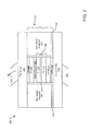
- FIG. 1 illustrates a schematic block diagram illustrating an example read head including a magnetoresistive sensor.
- FIG. 2 illustrates an alternative schematic block diagram illustrating an example read head including a magnetoresistive sensor.
- FIG. 3 illustrates example operations illustrating manufacturing a read head including a magnetoresistive sensor.
- FIG. 4 illustrates alternative example operations illustrating manufacturing a read head including a magnetoresistive sensor.
- FIG. 5 illustrates a graph illustrating the TMR improvements achieved by the read head manufactured using the process described herein.
- MR Thin film magnetoresistive
- MgO barriers and combined magnetic tunnel junction (MTJ) stack contributes significant signal to noise (SNR) gains that helps to close the performance gaps for product platforms.
- SNR signal to noise
- One method for improving the SNR and to reduce track misregistration values is to process materials at temperatures higher than room temperature by using an annealing process.
- Annealing is a heat treatment process that causes alternation in a material, causing changes in the property of the material, such as strength and hardness.
- Metallurgical annealing may include generating conditions for heating a material to above the recrystallization temperature of the material, maintaining a stable temperature above the recrystallization temperature of the material, and cooling the material.
- Such annealing process may be used to induce ductility, to soften material, to relieve internal stresses, to make the structure of the material more homogeneous, etc., for one or more layers of a sensor stack. For example, in one implementation of the process of manufacturing MR sensors a film is deposited on to wafers at elevated temperatures and an ex-situ post-deposition vacuum anneal is performed.
- ex-situ vacuum anneal is a slow process requiring slow ramp-up and slow ramp-down.
- the process of manufacturing MR sensor stack is delayed when such ex-situ vacuum annealing is used.
- using in-situ thermal anneal requiring longer ramp-up periods may result in diffusion of material across layers of the sensor stack.
- an in-situ rapid thermal anneal is inserted into one or more places during a deposition sequence.
- In situ thermal annealing is generally not used in recording head fabrication for a number of reasons. Specifically, when wafer processing is done at room temperature, any necessary high temperature processing is handled by ex-situ annealing in batch anneal ovens. Such separate processing provides simple and efficient manufacturing process. However, as the demand for the recording devices performance has increased, such devices require performance improvements.
- the methods described herein provide in-situ rapid thermal annealing configured to work with various sensor stack structures. Using in-situ rapid thermal annealing during the manufacturing of sensor stack results in higher quality sensor stacks that exhibit higher tunneling magnetoresistance (TMR) and better stability.
- TMR tunneling magnetoresistance
- an in-situ rapid thermal anneal (RTA) module is used to provide in-situ thermal annealing.
- the RTA module may be docked onto the sensor stack tool to allow for in-situ thermal anneal during any part of the stack deposition sequence.
- the RTA module also allows a magnetic field that allows for field cooling.
- Such in-situ RTA does not require first ramping up of the temperature of the material to be annealed over long time period and it requires shorter soak time for cooling the material after heat induced annealing.
- RTA module uses a heated chuck with electrostatic wafer clamping that can heat wafers in-situ.
- the RTA module can be docked on to a reader stack tool to provide in-situ thermal annealing at any part of stack deposition sequence.
- Such implementation of the RTA module allows rapid heat transfer to a particular layer of the reader stack.
- RTA module also provides a magnetic field that allows for in the field cooling of an annealed layer of the reader stack.
- a seed layer of a sensor stack is annealed at high temperature.
- high temperature annealing of the seed layer can be used in situations where subsequent layers of a sensor stack, such as layers of current perpendicular to plane giant magnetoresistive (CPP GMR) stacks, cannot be subjected to high temperatures.
- CPP GMR plane giant magnetoresistive
- different variations of the in-situ thermal anneal can be applied to the layers around a tunnel barrier layer of a sensor stack, such as an MgO tunnel barrier layer of a sensor stack. For example, annealing the bottom electrode of the tunnel barrier layer, annealing after the tunnel barrier layer is deposited, annealing after the top electrode of the tunnel barrier layer is deposited, etc.
- the in-situ thermal anneal may be applied at the end of the sensor stack sequence in order to exploit the fast thermal cycling.
- FIG. 1 illustrates a schematic block diagram illustrating an air-bearing surface (ABS) view of a tri-layer read head 100 including a magnetoresistive sensor 102 manufactured using in-situ thermal annealing disclosed herein.
- the sensor stack 102 is situated between a bottom shield 104 and a top shield 106.
- the magnetoresistive sensor 102 includes a seed layer 110 that is located at the bottom of the sensor stack 102.
- the seed layer 110 is deposited after etching a clean wafer surface using a plasma beam etching or ion-beam etching. In one implementation, after the seed layer 110 is deposited, it is annealed using in-situ thermal annealing.
- the seed layer 110 is an antiferromagnetic (AFM) seed layer.
- AFM antiferromagnetic
- the magnetoresistive sensor 102 also includes a first free layer (FL1) 112 adjacent to the seed layer 110.
- the free layer 112 is not exchange coupled to an antiferromagnet.
- the magnetoresistive sensor 102 further includes a tunneling barrier layer 114.
- the barrier layer 114 is an MgO barrier that provides magnetic tunnel junction (MTJ).
- the barrier layer is a metallic spacer that provides current perpendicular to plane giant magnetoresistance (CPP GMR).
- the barrier layer 114 is deposited at either room temperature or at higher temperatures in the range of 200 to 400 degree centigrade.
- the MgO barrier of the barrier layer 114 is broken up into a sequence of Mg, MgO, and Mg depositions.
- Such barrier layer 114 using Mg/MgO/Mg depositions is suited for use with low resistance area (RA) tunnel junctions.
- RA resistance area
- the barrier layer 114 may be annealed using in-situ thermal annealing mechanism. Furthermore, subsequent to the in-situ thermal annealing, the barrier layer 114 is cryo-cooled. Subsequently, a second free layer (FL2) 116 is deposited on top of the barrier layer 114. Thus, the barrier layer 114 in effect separates the first free layer FL1 112 from the second free layer FL2 116. A cap layer 118 is deposited on top of the second free layer FL2 116. In one implementation, after the cap layer 118 is treated using thermal in-situ annealing process.
- the read head 100 may optionally include side shields 120, which are insulated from the sensor stack 102 using insulation layers 122.
- the read head 100 is configured to fly over the surface of a disc drive data discs on an air bearing created by the rotation of the data discs.
- the data discs have a plurality of data tracks 150, one of which is shown in FIG. 1 .
- the tracks 150 are divided into a plurality of bits. As the disc rotates in the direction of the arrow 152, the read head 100 follows a data track 150 and reads one or more bits as it passes under magnetoresistive sensor 102.
- FIG. 2 illustrates a schematic block diagram illustrating an air-bearing surface (ABS) view of a high magnetoresistive barrier read head 200 including a magnetoresistive sensor 202 manufactured using in-situ thermal annealing disclosed herein.
- the sensor stack 202 is situated between a bottom shield 204 and a top shield 206.
- the magnetoresistive sensor 202 includes a seed layer 210 that is located at the bottom of the sensor stack 202.
- the seed layer 210 is deposited after etching a clean wafer surface using a plasma beam etching or ion-beam etching. In one implementation, after the seed layer 210 is deposited, it is annealed using in-situ thermal annealing.
- the magnetoresistive sensor 202 also includes an AFM layer 212 deposited on the seed layer 210.
- the AFM layer 212 may be an IrMn layer.
- the AFM layer 212 is annealed using an in-situ thermal anneal process.
- a part or all of a CoFe PL layer 216 is deposited on the annealed AFM layer 212.
- the PL layer 216 is also annealed using an in-situ thermal anneal process.
- the PL layer 216 is part of a synthetic antiferromagnetic (SAF) layer 214.
- SAF synthetic antiferromagnetic
- the magnetoresistive sensor 202 further includes a barrier layer 222.
- the barrier layer 222 is an MgO barrier that provides magnetic tunnel junction (MTJ).
- the barrier layer 222 is a metallic spacer that provides current perpendicular to plane giant magnetoresistance (CPP GMR).
- the barrier layer 222 is deposited at either room temperature or at higher temperatures in the range of 200 to 400 degree centigrade.
- the MgO barrier of the barrier layer 222 is broken up into a sequence of Mg, MgO, and Mg depositions.
- Such barrier layer 222 using Mg/MgO/Mg depositions is suited for use with low resistance area (RA) tunnel junctions.
- RA resistance area
- the barrier layer 222 may be annealed using in-situ thermal annealing mechanism. Furthermore, subsequent to the in-situ thermal annealing, the barrier layer 222 is cryo-cooled. Subsequently, a free layer (FL) 224 is deposited on top of the barrier layer 222. A cap layer 226 is deposited on top of the free layer FL 224. In one implementation, after the cap layer 226 is treated using thermal in-situ annealing process.
- the read head 200 includes side shields 230, which are insulated from the sensor stack 202 using insulation layers 232.
- the read head 200 is configured to fly over the surface of a disc drive data discs on an air bearing created by the rotation of the data discs.
- the data discs have a plurality of data tracks 250, one of which is shown in FIG. 2 .
- the tracks 250 are divided into a plurality of bits. As the disc rotates in the direction of the arrow 252, the read head 200 follows a data track 250 and reads one or more bits as it passes under magnetoresistive sensor 202.
- FIG. 3 illustrates example operations 300 illustrating manufacturing of a read head including a magnetoresistive sensor.
- the operations 300 illustrate a method of manufacturing a magnetoresistive sensor for a trilayer read head.
- An etching operation 302 etches a clean wafer surface using plasma etching or ion-beam etching technique.
- a depositing operation 304 deposits a seed layer on the etched wafer surface.
- an annealing operation 306 anneals the seed layer using in-situ thermal anneal process.
- RTA rapid thermal anneal
- an operation 308 deposits a first free layer on the seed layer.
- such free layer is not exchange coupled to an antiferromagnet.
- the magnetic moment of the free layer is free to rotate under the influence of an applied magnetic field in a range of interest.
- a depositing operation 310 deposits a barrier layer.
- the barrier layer is deposited at 200 °C.
- Example barrier layer may be made of MgO material that provides an MTJ.
- the depositing the MgO layer can be broken up into a sequence of depositions, with first being depositing of an Mg layer, subsequently depositing an MgO layer, and finally depositing another Mg layer.
- a metallic spacer layer is deposited, wherein such metallic spacer layer provides CPP GMR.
- An annealing operation 312 performs in-situ rapid thermal annealing of the barrier/spacer layer.
- a cooling operation 314 applies cryo-cooling after the annealing operation.
- the in-situ rapid thermal annealing of the barrier/spacer layer allows rapid cooling of the annealed layers.
- a depositing operation 316 deposits a second free layer on the annealed barrier/spacer layer.
- a cap layer is deposited on top of the second free layer during a depositing operation 318.
- an annealing operation 320 anneals the cap layer.
- FIG. 4 illustrates alternative example operations illustrating manufacturing a read head including a magnetoresistive sensor.
- the operations 400 illustrate a method of manufacturing a magnetoresistive sensor for a trilayer read head.
- An etching operation 402 etches a clean wafer surface using plasma etching or ion-beam etching technique.
- a depositing operation 404 deposits a seed layer on the etched wafer surface.
- an annealing operation 406 anneals the seed layer using in-situ thermal anneal process.
- RTA rapid thermal anneal
- a depositing operation 408 deposits an antiferromagnetic (AFM) layer on the seed layer.
- the AFM layer may be an IrMn layer.
- the AFM layer is annealed using an in-situ rapid thermal anneal process by an annealing operation 410.
- the application of in-situ rapid thermal annealing after deposition of an IrMn layer leads to improved pinning. Specifically, the in-situ anneal prevents Mn from diffusing and leads to more ordered and clean IrMn layer.
- a depositing operation 412 deposits an SAF layer on the annealed AFM layer.
- a depositing operation 414 deposits a barrier layer.
- the barrier layer is deposited at 200 °C.
- Example barrier layer may be made of MgO material that provides an MTJ.
- the depositing the MgO layer can be broken up into a sequence of depositions, with first being depositing of an Mg layer, subsequently depositing an MgO layer, and finally depositing another Mg layer.
- a metallic spacer layer is deposited, wherein such metallic spacer layer provides CPP GMR.
- An annealing operation 416 performs in-situ rapid thermal annealing of the barrier/spacer layer.
- a cooling operation (not shown) applies cryo-cooling after the annealing operation.
- the in-situ rapid thermal annealing of the barrier/spacer layer allows rapid cooling of the annealed layers.
- a depositing operation 418 deposits a free layer on the annealed barrier/spacer layer.
- a cap layer is deposited on top of the second free layer during a depositing operation 420.
- an annealing operation 422 anneals the cap layer.
- Annealing one or more layers of a sensor stack at a high temperature using in-situ rapid thermal annealing increases the magnetoresistance (MR) in the MgO based magnetic tunnel junctions (MTJs) and in thin films made of other materials such as ordered Heusler alloys.
- MR magnetoresistance
- MgO based magnetic tunnel junctions MgO based magnetic tunnel junctions
- TMR tunneling magnetoresistance
- FIG. 5 illustrates a graph 500 illustrating the improvement in the TMR achieved by the read head manufactured using the process described herein.
- the graph 500 illustrates the TMR for various combinations of temperature and times for the in-situ rapid thermal annealing (RTA) applied to a layer of a trilayer sensor stack.
- RTA rapid thermal annealing
- the graph 500 illustrates that when in-situ RTA is applied with the annealing temperature of 400 degrees centigrade over a soak time of 60 seconds, the TMR 502 of 161 is achieved.
- the annealing temperature is increased to 450 degrees centigrade over a soak time of 60 seconds, the TMR 504 increases to 177.
- large TMR enhancements are achieved in short time periods by going to temperatures higher than 300 degree centigrade. However, when the annealing temperature is increased to the range of 500 degree centigrade, the TMR declines.
- TMR data shown in FIG. 5 illustrates improvements in the TMR for a trilayer sensor stack, similar increases in TMR are also observed in other sensor stacks.
- Using the in-situ rapid thermal annealing for one or more layers of sensor stacks also allows in using smaller soak time for cooling the annealed layers.
- the shorter cooling periods result in smaller standard deviations for the resistance area (RA).
- in-situ thermal anneals can applied to reader materials including shields, dielectrics for electric isolation, permanent magnets, etc.
- in-situ thermal anneals can be applied to any of the magnetic layers that form part of a writer, including the writer, the coil, the dielectrics, the non-magnetic metals, etc.
- the in-situ anneal process can also be applied in other situations where materials need to anneal but suffer inter-diffusion with capping materials.
- an in-situ anneal operation is inserted between the deposition of the material in question and the deposition of the capping layer.
- the fast turn-around times of the in-situ anneal process and in-situ rapid thermal anneal process results in relatively small addition of process time.
- the in-situ anneal process disclosed herein can be further expanded to include on-wafer designs that manage the absorption of the infrared radiation from rapid-thermal anneal lamps.
- reflector layers are put down in order to shield more critical parts of the wafer.
- Such reflectors can have appropriate thermal design that thermally isolates them from the sensitive parts of the wafer.
- the device area that is targeted for anneal can also undergo thermal engineering that provides a thermally connected heat sink with a large thermal mass that functions as a heat sink to enable rapid cooling of the device area once the rapid thermal annealing lamp is turned off.
- Other manners of heat sink are also provided in alternative implementations.
Landscapes
- Physics & Mathematics (AREA)
- Condensed Matter Physics & Semiconductors (AREA)
- General Physics & Mathematics (AREA)
- Engineering & Computer Science (AREA)
- Manufacturing & Machinery (AREA)
- Magnetic Heads (AREA)
- Hall/Mr Elements (AREA)
Abstract
Description
- In a magnetic data storage and retrieval system, a magnetic read/write head typically includes a reader portion having a magnetoresistive (MR) sensor for retrieving magnetically encoded information stored on a magnetic disc. Magnetic flux from the surface of the disc causes rotation of the magnetization vector of a sensing layer of the MR sensor, which in turn causes a change in electrical resistivity of the MR sensor. The change in resistivity of the MR sensor can be detected by passing a current through the MR sensor and measuring a voltage across the MR sensor. External circuitry then converts the voltage information into an appropriate format and manipulates that information as necessary to recover the information encoded on the disc.
- Implementations described and claimed herein provide a sensor stack including at least one layer that is annealed using rapid thermal annealing after its deposition. In one implementation of the magnetic sensor a seed layer is annealed using in-situ rapid thermal annealing. Alternatively, one of a barrier layer, an AFM layer, and a cap layer is annealed using in-situ rapid thermal annealing.
- This Summary is provided to introduce a selection of concepts in a simplified form that are further described below in the Detailed Description. This Summary is not intended to identify key features or essential features of the claimed subject matter, nor is it intended to be used to limit the scope of the claimed subject matter. Other features, details, utilities, and advantages of the claimed subject matter will be apparent from the following more particular written Detailed Description of various implementations and implementations as further illustrated in the accompanying drawings and defined in the appended claims.
- According to a first aspect of the present invention, there is provided a method of making a sensor stack, comprising: annealing at least two layers of the sensor stack using in-situ rapid thermal annealing.
- Preferably, the annealing at least two layers of the sensor stack using in-situ rapid thermal annealing comprises annealing a seed layer using in-situ rapid thermal annealing.
- Preferably, the annealing at least two layers of the sensor stack using in-situ rapid thermal annealing comprises annealing an MgO barrier layer using in-situ rapid thermal annealing.
- Preferably, the annealing at least two layers of the sensor stack using in-situ rapid thermal annealing comprises annealing an MgO barrier layer using in-situ rapid thermal annealing, wherein the MgO barrier layer is deposited between two Mg layers.
- Preferably, the annealing at least two layers of the sensor stack using in-situ rapid thermal annealing comprises annealing a metallic spacer layer using in-situ rapid thermal annealing.
- In this case, the method preferably further comprises cryo-cooling the MgO barrier layer.
- Preferably, the annealing at least two layers of the sensor stack using in-situ rapid thermal annealing comprises annealing an AFM layer using in-situ rapid thermal annealing.
- In this case, it is preferred that the AFM layer is an IrMn layer.
- According to a further aspect of the present invention, there is provided a method of making a sensor stack, comprising: etching a surface; depositing a seed layer over the surface; and annealing the seed layer using in-situ thermal annealing.
- Preferably, the method further comprises depositing an AFM layer on top of the annealed seed layer; and annealing the AFM layer using in-situ thermal annealing.
- Preferably, the method further comprises depositing an SAF layer on top of the annealed AFM layer; depositing a free layer; and depositing a cap layer on top of the free layer.
- In this case, it is preferred that the method further comprises annealing the cap layer using in-situ thermal annealing.
- It is also preferred that the method further comprises depositing an MgO barrier layer on top of the SAF layer; and annealing the MgO barrier layer using in-situ thermal annealing.
- Depositing the MgO barrier layer may further comprise depositing an Mg layer on top of the SAF layer; depositing an MgO barrier layer on top of the Mg layer; and depositing an Mg layer on top of the MgO barrier layer.
- Preferably, the method further comprises depositing a metallic spacer layer on top of the SAF layer; annealing the metallic spacer layer using in-situ thermal annealing; and cryo cooling the annealed metallic spacer layer.
- Depositing the metallic spacer layer may further comprise depositing the metallic spacer layer at a temperature within a range of 200 to 400 degrees centigrade.
- Preferably, the method of this aspect further comprises rapidly cooling the annealed seed layer using a thermally connected heat sink with a large thermal mass.
- According to a further aspect of the present invention, there is provided a read head comprising: a first shield layer; a second shield layer; and a sensor stack located between the first shield layer and the second shield layer, the sensor stack having a plurality of layers wherein at least one layer is annealed using in-situ rapid thermal annealing.
- Preferably, the at least one layer annealed using in-situ rapid thermal annealing is a seed layer.
- Preferably, the sensor stack further comprises:
- a barrier layer annealed using in-situ rapid thermal annealing; and
- a cap layer annealed using in-situ rapid thermal annealing.
- According to a yet further aspect of the present invention, there is provided a sensor stack prepared by a process comprising: etching a surface; depositing a seed layer on the surface; and annealing the seed layer using in-situ rapid thermal annealing.
- Preferably, the process further comprises depositing an AFM layer on the annealed seed layer; annealing the AFM layer using in-situ thermal annealing; depositing an SAF layer on the annealed AFM layer; depositing a free layer on the annealed AFM layer; depositing a cap layer on the free layer; and annealing the cap layer using in-situ thermal annealing.
- These and various other features and advantages will be apparent from a reading of the following detailed description.
-
FIG. 1 illustrates a schematic block diagram illustrating an example read head including a magnetoresistive sensor. -
FIG. 2 illustrates an alternative schematic block diagram illustrating an example read head including a magnetoresistive sensor. -
FIG. 3 illustrates example operations illustrating manufacturing a read head including a magnetoresistive sensor. -
FIG. 4 illustrates alternative example operations illustrating manufacturing a read head including a magnetoresistive sensor. -
FIG. 5 illustrates a graph illustrating the TMR improvements achieved by the read head manufactured using the process described herein. - There is an ever increasing demand for high data densities that require sensitive sensors to read data from a magnetic media. Thin film magnetoresistive (MR) multilayers form the heart of MR readers and their quality has a very strong impact on reader performance. For example, improvements in the MgO barriers and combined magnetic tunnel junction (MTJ) stack contributes significant signal to noise (SNR) gains that helps to close the performance gaps for product platforms. One method for improving the SNR and to reduce track misregistration values is to process materials at temperatures higher than room temperature by using an annealing process.
- Annealing is a heat treatment process that causes alternation in a material, causing changes in the property of the material, such as strength and hardness. Metallurgical annealing may include generating conditions for heating a material to above the recrystallization temperature of the material, maintaining a stable temperature above the recrystallization temperature of the material, and cooling the material. Such annealing process may be used to induce ductility, to soften material, to relieve internal stresses, to make the structure of the material more homogeneous, etc., for one or more layers of a sensor stack. For example, in one implementation of the process of manufacturing MR sensors a film is deposited on to wafers at elevated temperatures and an ex-situ post-deposition vacuum anneal is performed. Such manufacturing process leads to higher quality MgO barriers. However, ex-situ vacuum anneal is a slow process requiring slow ramp-up and slow ramp-down. As a result, the process of manufacturing MR sensor stack is delayed when such ex-situ vacuum annealing is used. On the other hand, using in-situ thermal anneal requiring longer ramp-up periods may result in diffusion of material across layers of the sensor stack.
- In an implementation of the process of manufacturing MR sensor stack disclosed herein, an in-situ rapid thermal anneal is inserted into one or more places during a deposition sequence. In situ thermal annealing is generally not used in recording head fabrication for a number of reasons. Specifically, when wafer processing is done at room temperature, any necessary high temperature processing is handled by ex-situ annealing in batch anneal ovens. Such separate processing provides simple and efficient manufacturing process. However, as the demand for the recording devices performance has increased, such devices require performance improvements. The methods described herein provide in-situ rapid thermal annealing configured to work with various sensor stack structures. Using in-situ rapid thermal annealing during the manufacturing of sensor stack results in higher quality sensor stacks that exhibit higher tunneling magnetoresistance (TMR) and better stability.
- In one implementation, an in-situ rapid thermal anneal (RTA) module is used to provide in-situ thermal annealing. The RTA module may be docked onto the sensor stack tool to allow for in-situ thermal anneal during any part of the stack deposition sequence. Furthermore, the RTA module also allows a magnetic field that allows for field cooling. Such in-situ RTA does not require first ramping up of the temperature of the material to be annealed over long time period and it requires shorter soak time for cooling the material after heat induced annealing.
- Another implementation uses a heated chuck with electrostatic wafer clamping that can heat wafers in-situ. In an alternative implementation, the RTA module can be docked on to a reader stack tool to provide in-situ thermal annealing at any part of stack deposition sequence. Thus, such implementation allows thermal annealing of a seed layer of the reader stack, a barrier layer of the reader stack, a cap layer of the reader stack, etc. Such implementation of the RTA module allows rapid heat transfer to a particular layer of the reader stack. Furthermore, such RTA module also provides a magnetic field that allows for in the field cooling of an annealed layer of the reader stack.
- In an example implementation, a seed layer of a sensor stack is annealed at high temperature. For example, such high temperature annealing of the seed layer can be used in situations where subsequent layers of a sensor stack, such as layers of current perpendicular to plane giant magnetoresistive (CPP GMR) stacks, cannot be subjected to high temperatures. In an alternative implementation, different variations of the in-situ thermal anneal can be applied to the layers around a tunnel barrier layer of a sensor stack, such as an MgO tunnel barrier layer of a sensor stack. For example, annealing the bottom electrode of the tunnel barrier layer, annealing after the tunnel barrier layer is deposited, annealing after the top electrode of the tunnel barrier layer is deposited, etc. Yet alternatively, the in-situ thermal anneal may be applied at the end of the sensor stack sequence in order to exploit the fast thermal cycling.
-
FIG. 1 illustrates a schematic block diagram illustrating an air-bearing surface (ABS) view of atri-layer read head 100 including amagnetoresistive sensor 102 manufactured using in-situ thermal annealing disclosed herein. Specifically, thesensor stack 102 is situated between abottom shield 104 and atop shield 106. Themagnetoresistive sensor 102 includes aseed layer 110 that is located at the bottom of thesensor stack 102. Theseed layer 110 is deposited after etching a clean wafer surface using a plasma beam etching or ion-beam etching. In one implementation, after theseed layer 110 is deposited, it is annealed using in-situ thermal annealing. In one example implementation, theseed layer 110 is an antiferromagnetic (AFM) seed layer. - The
magnetoresistive sensor 102 also includes a first free layer (FL1) 112 adjacent to theseed layer 110. In one implementation, thefree layer 112 is not exchange coupled to an antiferromagnet. As a result, the magnetic moment of thefree layer 112 is free to rotate under the influence of an applied magnetic field in a range of interest. Themagnetoresistive sensor 102 further includes atunneling barrier layer 114. In one implementation, thebarrier layer 114 is an MgO barrier that provides magnetic tunnel junction (MTJ). In an alternative implementation the barrier layer is a metallic spacer that provides current perpendicular to plane giant magnetoresistance (CPP GMR). Thebarrier layer 114 is deposited at either room temperature or at higher temperatures in the range of 200 to 400 degree centigrade. Yet alternatively, the MgO barrier of thebarrier layer 114 is broken up into a sequence of Mg, MgO, and Mg depositions.Such barrier layer 114 using Mg/MgO/Mg depositions is suited for use with low resistance area (RA) tunnel junctions. - The
barrier layer 114 may be annealed using in-situ thermal annealing mechanism. Furthermore, subsequent to the in-situ thermal annealing, thebarrier layer 114 is cryo-cooled. Subsequently, a second free layer (FL2) 116 is deposited on top of thebarrier layer 114. Thus, thebarrier layer 114 in effect separates the firstfree layer FL1 112 from the secondfree layer FL2 116. Acap layer 118 is deposited on top of the secondfree layer FL2 116. In one implementation, after thecap layer 118 is treated using thermal in-situ annealing process. - The read
head 100 may optionally include side shields 120, which are insulated from thesensor stack 102 using insulation layers 122. The readhead 100 is configured to fly over the surface of a disc drive data discs on an air bearing created by the rotation of the data discs. The data discs have a plurality ofdata tracks 150, one of which is shown inFIG. 1 . Thetracks 150 are divided into a plurality of bits. As the disc rotates in the direction of thearrow 152, theread head 100 follows adata track 150 and reads one or more bits as it passes undermagnetoresistive sensor 102. -
FIG. 2 illustrates a schematic block diagram illustrating an air-bearing surface (ABS) view of a high magnetoresistive barrier readhead 200 including amagnetoresistive sensor 202 manufactured using in-situ thermal annealing disclosed herein. Specifically, thesensor stack 202 is situated between abottom shield 204 and atop shield 206. Themagnetoresistive sensor 202 includes aseed layer 210 that is located at the bottom of thesensor stack 202. Theseed layer 210 is deposited after etching a clean wafer surface using a plasma beam etching or ion-beam etching. In one implementation, after theseed layer 210 is deposited, it is annealed using in-situ thermal annealing. - The
magnetoresistive sensor 202 also includes anAFM layer 212 deposited on theseed layer 210. TheAFM layer 212 may be an IrMn layer. Subsequently, theAFM layer 212 is annealed using an in-situ thermal anneal process. A part or all of aCoFe PL layer 216 is deposited on the annealedAFM layer 212. In one implementation, thePL layer 216 is also annealed using an in-situ thermal anneal process. - The
PL layer 216 is part of a synthetic antiferromagnetic (SAF)layer 214. In one implementation remainder of theSAF layer 214, includes anRu layer 218 and anRL layer 220 deposited on top of thePL layer 216. Themagnetoresistive sensor 202 further includes abarrier layer 222. In one implementation, thebarrier layer 222 is an MgO barrier that provides magnetic tunnel junction (MTJ). In an alternative implementation thebarrier layer 222 is a metallic spacer that provides current perpendicular to plane giant magnetoresistance (CPP GMR). Thebarrier layer 222 is deposited at either room temperature or at higher temperatures in the range of 200 to 400 degree centigrade. Yet alternatively, the MgO barrier of thebarrier layer 222 is broken up into a sequence of Mg, MgO, and Mg depositions.Such barrier layer 222 using Mg/MgO/Mg depositions is suited for use with low resistance area (RA) tunnel junctions. - The
barrier layer 222 may be annealed using in-situ thermal annealing mechanism. Furthermore, subsequent to the in-situ thermal annealing, thebarrier layer 222 is cryo-cooled. Subsequently, a free layer (FL) 224 is deposited on top of thebarrier layer 222. Acap layer 226 is deposited on top of the free layer FL 224. In one implementation, after thecap layer 226 is treated using thermal in-situ annealing process. - The read
head 200 includes side shields 230, which are insulated from thesensor stack 202 using insulation layers 232. The readhead 200 is configured to fly over the surface of a disc drive data discs on an air bearing created by the rotation of the data discs. The data discs have a plurality ofdata tracks 250, one of which is shown inFIG. 2 . Thetracks 250 are divided into a plurality of bits. As the disc rotates in the direction of thearrow 252, theread head 200 follows adata track 250 and reads one or more bits as it passes undermagnetoresistive sensor 202. -
FIG. 3 illustratesexample operations 300 illustrating manufacturing of a read head including a magnetoresistive sensor. Specifically, theoperations 300 illustrate a method of manufacturing a magnetoresistive sensor for a trilayer read head. Anetching operation 302 etches a clean wafer surface using plasma etching or ion-beam etching technique. Subsequently, adepositing operation 304 deposits a seed layer on the etched wafer surface. In one implementation, anannealing operation 306 anneals the seed layer using in-situ thermal anneal process. For example, such in-situ thermal annealing is provided using an in-situ rapid thermal anneal (RTA) module. - Subsequently, an
operation 308 deposits a first free layer on the seed layer. In one implementation, such free layer is not exchange coupled to an antiferromagnet. As a result, the magnetic moment of the free layer is free to rotate under the influence of an applied magnetic field in a range of interest. Subsequently, adepositing operation 310 deposits a barrier layer. In one implementation, the barrier layer is deposited at 200 °C. Example barrier layer may be made of MgO material that provides an MTJ. In one implementation, the depositing the MgO layer can be broken up into a sequence of depositions, with first being depositing of an Mg layer, subsequently depositing an MgO layer, and finally depositing another Mg layer. In yet alternative implementation, instead of a barrier layer, a metallic spacer layer is deposited, wherein such metallic spacer layer provides CPP GMR. - An annealing operation 312 performs in-situ rapid thermal annealing of the barrier/spacer layer. Optionally, a cooling operation 314 applies cryo-cooling after the annealing operation. The in-situ rapid thermal annealing of the barrier/spacer layer allows rapid cooling of the annealed layers. Subsequently, a depositing operation 316 deposits a second free layer on the annealed barrier/spacer layer. A cap layer is deposited on top of the second free layer during a
depositing operation 318. Finally, anannealing operation 320 anneals the cap layer. - Note that while the
operations 300 illustrate applying in-situ thermal annealing of various specific layers, such as the seed layer, the barrier layer, the cap layer, etc., in an alternative implementation not all of these layers are annealed. Furthermore, in yet alternative implementation, other layers of the magnetoresistive sensor may also be annealed after deposition of such layers. -
FIG. 4 illustrates alternative example operations illustrating manufacturing a read head including a magnetoresistive sensor. Specifically, theoperations 400 illustrate a method of manufacturing a magnetoresistive sensor for a trilayer read head. Anetching operation 402 etches a clean wafer surface using plasma etching or ion-beam etching technique. Subsequently, adepositing operation 404 deposits a seed layer on the etched wafer surface. In one implementation, anannealing operation 406 anneals the seed layer using in-situ thermal anneal process. For example, such in-situ thermal annealing is provided using an in-situ rapid thermal anneal (RTA) module. - Subsequently, a depositing operation 408 deposits an antiferromagnetic (AFM) layer on the seed layer. The AFM layer may be an IrMn layer. Subsequently, the AFM layer is annealed using an in-situ rapid thermal anneal process by an annealing operation 410. The application of in-situ rapid thermal annealing after deposition of an IrMn layer leads to improved pinning. Specifically, the in-situ anneal prevents Mn from diffusing and leads to more ordered and clean IrMn layer. After annealing the AFM layer, a depositing operation 412 deposits an SAF layer on the annealed AFM layer.
- Subsequently, a
depositing operation 414 deposits a barrier layer. In one implementation, the barrier layer is deposited at 200 °C. Example barrier layer may be made of MgO material that provides an MTJ. In one implementation, the depositing the MgO layer can be broken up into a sequence of depositions, with first being depositing of an Mg layer, subsequently depositing an MgO layer, and finally depositing another Mg layer. In yet alternative implementation, instead of a barrier layer, a metallic spacer layer is deposited, wherein such metallic spacer layer provides CPP GMR. - An
annealing operation 416 performs in-situ rapid thermal annealing of the barrier/spacer layer. Optionally, a cooling operation (not shown) applies cryo-cooling after the annealing operation. The in-situ rapid thermal annealing of the barrier/spacer layer allows rapid cooling of the annealed layers. Subsequently, adepositing operation 418 deposits a free layer on the annealed barrier/spacer layer. A cap layer is deposited on top of the second free layer during adepositing operation 420. Finally, anannealing operation 422 anneals the cap layer. - Note that while the
operations 400 illustrate applying in-situ thermal annealing of various specific layers, such as the seed layer, the barrier layer, the cap layer, etc., in an alternative implementation not all of these layers are annealed. Furthermore, in yet alternative implementation, other layers of the magnetoresistive sensor may also be annealed after deposition of such layers. - Annealing one or more layers of a sensor stack at a high temperature using in-situ rapid thermal annealing increases the magnetoresistance (MR) in the MgO based magnetic tunnel junctions (MTJs) and in thin films made of other materials such as ordered Heusler alloys. For example, for MgO based trilayer type sensor stacks, increasing post-deposition anneal temperature to approximately 450 degree centigrade results in substantially increasing the tunneling magnetoresistance (TMR).
-
FIG. 5 illustrates agraph 500 illustrating the improvement in the TMR achieved by the read head manufactured using the process described herein. Specifically, thegraph 500 illustrates the TMR for various combinations of temperature and times for the in-situ rapid thermal annealing (RTA) applied to a layer of a trilayer sensor stack. For example, thegraph 500 illustrates that when in-situ RTA is applied with the annealing temperature of 400 degrees centigrade over a soak time of 60 seconds, theTMR 502 of 161 is achieved. When the annealing temperature is increased to 450 degrees centigrade over a soak time of 60 seconds, theTMR 504 increases to 177. As illustrated inFIG. 5 , large TMR enhancements are achieved in short time periods by going to temperatures higher than 300 degree centigrade. However, when the annealing temperature is increased to the range of 500 degree centigrade, the TMR declines. - While the TMR data shown in
FIG. 5 illustrates improvements in the TMR for a trilayer sensor stack, similar increases in TMR are also observed in other sensor stacks. - Using the in-situ rapid thermal annealing for one or more layers of sensor stacks also allows in using smaller soak time for cooling the annealed layers. The shorter cooling periods result in smaller standard deviations for the resistance area (RA).
- Even though the concepts of in-situ thermal anneal in general and the in-situ rapid thermal anneal are discussed above with respect to sensor stacks for read heads, in alternative implementations, these concepts are applied in even broader range of applications in recording head fabrication. For example, in-situ thermal anneals can applied to reader materials including shields, dielectrics for electric isolation, permanent magnets, etc. For writers, in-situ thermal anneals can be applied to any of the magnetic layers that form part of a writer, including the writer, the coil, the dielectrics, the non-magnetic metals, etc. The in-situ anneal process can also be applied in other situations where materials need to anneal but suffer inter-diffusion with capping materials. In these implementations, an in-situ anneal operation is inserted between the deposition of the material in question and the deposition of the capping layer. In such implementations, the fast turn-around times of the in-situ anneal process and in-situ rapid thermal anneal process results in relatively small addition of process time.
- Furthermore, the in-situ anneal process disclosed herein can be further expanded to include on-wafer designs that manage the absorption of the infrared radiation from rapid-thermal anneal lamps. For example, in example implementations, reflector layers are put down in order to shield more critical parts of the wafer. Such reflectors can have appropriate thermal design that thermally isolates them from the sensitive parts of the wafer. In yet alternative implementation, the device area that is targeted for anneal can also undergo thermal engineering that provides a thermally connected heat sink with a large thermal mass that functions as a heat sink to enable rapid cooling of the device area once the rapid thermal annealing lamp is turned off. Other manners of heat sink are also provided in alternative implementations.
- The above specification, examples, and data provide a complete description of the structure and use of example implementations of the invention. Since many implementations of the invention can be made without departing from the spirit and scope of the invention, the invention resides in the claims hereinafter appended. Furthermore, structural features of the different implementations may be combined in yet another implementation without departing from the recited claims. The implementations described above and other implementations are within the scope of the following claims.
Claims (20)
- A method of making a sensor stack, comprising:(306, 312, 320; 406, 410, 416, 422) annealing at least two layers of the sensor stack (102, 202) using in-situ rapid thermal annealing.
- The method of claim 1 wherein the annealing at least two layers of the sensor stack using in-situ rapid thermal annealing comprises (306, 406) annealing a seed layer (110, 210) using in-situ rapid thermal annealing.
- The method of claim 1 or claim 2 wherein the annealing at least two layers of the sensor stack using in-situ rapid thermal annealing comprises (312, 416) annealing an MgO barrier layer (114, 222) using in-situ rapid thermal annealing.
- The method of claim 3 wherein the MgO barrier layer is deposited between two Mg layers.
- The method of claim 3 or claim 4 further comprising (314) cryo-cooling the MgO barrier layer.
- The method of claim 1 or claim 2 wherein the annealing at least two layers of the sensor stack using in-situ rapid thermal annealing comprises (312, 416) annealing a metallic spacer layer (114, 222) using in-situ rapid thermal annealing.
- The method of any one of the preceding claims wherein the annealing at least two layers of the sensor stack using in-situ rapid thermal annealing comprises (410) annealing an AFM layer (212) using in-situ rapid thermal annealing.
- The method of claim 7 wherein the AFM layer is an IrMn layer.
- A method of making a sensor stack (102), comprising:(302, 402) etching a surface;(304, 404) depositing a seed layer (110, 210) over the surface; and(306, 406) annealing the seed layer using in-situ thermal annealing.
- The method of claim 9, further comprising:(408) depositing an AFM layer (212) on top of the annealed seed layer; and(410) annealing the AFM layer using in-situ thermal annealing.
- The method of claim 10, further comprising:(412) depositing an SAF layer (214) on top of the annealed AFM layer;(418) depositing a free layer (224); and(420) depositing a cap layer (226) on top of the free layer.
- The method of claim 11 further comprising (422) annealing the cap layer using in-situ thermal annealing.
- The method of claim 11 or claim 12 further comprising:(414) depositing an MgO barrier layer (222) on top of the SAF layer; and(416) annealing the MgO barrier layer using in-situ thermal annealing.
- The method of claim 13 wherein depositing the MgO barrier layer further comprises:depositing an Mg layer on top of the SAF layer (214);depositing an MgO barrier layer on top of the Mg layer; anddepositing an Mg layer on top of the MgO barrier layer.
- The method of any one of claims 11 to 14 further comprising:(414) depositing a metallic spacer layer (222) on top of the SAF layer;(416) annealing the metallic spacer layer using in-situ thermal annealing; and
cryo cooling the annealed metallic spacer layer. - The method of claim 15 wherein depositing the metallic spacer layer (222) further comprises depositing the metallic spacer layer at a temperature within a range of 200 to 400 degrees centigrade.
- The method of any one of claims 10 to 16 further comprising rapidly cooling the annealed seed layer using a thermally connected heat sink with a large thermal mass.
- A read head (100, 200) comprising:a first shield layer (104, 204);a second shield layer (106, 206); anda sensor stack (102, 202) located between the first shield layer and the second shield layer, the sensor stack having a plurality of layers wherein at least one layer is annealed using in-situ rapid thermal annealing.
- The read head of claim 18 wherein the at least one layer annealed using in-situ rapid thermal annealing is a seed layer (110, 210).
- The read head of claim 19 wherein the sensor stack further comprises:a barrier layer (114, 222) annealed using in-situ rapid thermal annealing; anda cap layer (118, 226) annealed using in-situ rapid thermal annealing.
Applications Claiming Priority (1)
| Application Number | Priority Date | Filing Date | Title |
|---|---|---|---|
| US13/419,728 US9880232B2 (en) | 2012-03-14 | 2012-03-14 | Magnetic sensor manufacturing |
Publications (2)
| Publication Number | Publication Date |
|---|---|
| EP2639593A1 true EP2639593A1 (en) | 2013-09-18 |
| EP2639593B1 EP2639593B1 (en) | 2016-11-16 |
Family
ID=47901783
Family Applications (1)
| Application Number | Title | Priority Date | Filing Date |
|---|---|---|---|
| EP13159039.0A Not-in-force EP2639593B1 (en) | 2012-03-14 | 2013-03-13 | Magnetic sensor manufacturing |
Country Status (5)
| Country | Link |
|---|---|
| US (3) | US9880232B2 (en) |
| EP (1) | EP2639593B1 (en) |
| JP (1) | JP2013191268A (en) |
| KR (1) | KR101456995B1 (en) |
| CN (1) | CN103310804A (en) |
Cited By (2)
| Publication number | Priority date | Publication date | Assignee | Title |
|---|---|---|---|---|
| US9880232B2 (en) | 2012-03-14 | 2018-01-30 | Seagate Technology Llc | Magnetic sensor manufacturing |
| EP3291318A4 (en) * | 2015-04-27 | 2019-01-23 | Multidimension Technology Co., Ltd. | METHOD AND APPARATUS FOR QUICK THERMAL TREATMENT FOR SPINTRONIC DEVICE TRAPPING LAYER |
Families Citing this family (14)
| Publication number | Priority date | Publication date | Assignee | Title |
|---|---|---|---|---|
| US8852963B2 (en) * | 2013-02-12 | 2014-10-07 | HGST Netherlands B.V. | Method for making a current-perpendicular-to-the-plane (CPP) magnetoresistive sensor having a low-coercivity reference layer |
| US9070869B2 (en) * | 2013-10-10 | 2015-06-30 | Avalanche Technology, Inc. | Fabrication method for high-density MRAM using thin hard mask |
| US9214172B2 (en) * | 2013-10-23 | 2015-12-15 | Western Digital (Fremont), Llc | Method of manufacturing a magnetic read head |
| US9305572B2 (en) | 2014-05-01 | 2016-04-05 | Seagate Technology Llc | Methods of forming portions of near field transducers (NFTS) and articles formed thereby |
| US9633679B2 (en) * | 2014-05-06 | 2017-04-25 | Seagate Technology Llc | Sensor stack structure with RKKY coupling layer between free layer and capping layer |
| US20170153125A1 (en) * | 2014-06-18 | 2017-06-01 | Mitsubishi Electric Corporation | Magnetic sensor device and method for producing same |
| US9559296B2 (en) | 2014-07-03 | 2017-01-31 | Samsung Electronics Co., Ltd. | Method for providing a perpendicular magnetic anisotropy magnetic junction usable in spin transfer torque magnetic devices using a sacrificial insertion layer |
| CN104659202A (en) * | 2015-02-13 | 2015-05-27 | 西南应用磁学研究所 | Preparation method for magnetic tunnel junction thin film capable of improving magneto-resistive effect |
| CN105938872A (en) * | 2016-06-02 | 2016-09-14 | 南京工业大学 | Magnetic tunnel junction structure and tunnel magnetoresistive element |
| EP3552250B1 (en) * | 2016-12-06 | 2025-10-29 | Everspin Technologies, Inc. | Method for manufacturing magnetoresistive devices |
| US9837106B1 (en) * | 2017-06-05 | 2017-12-05 | Western Digital Technologies, Inc. | Two-dimensional magnetic recording (TDMR) disk drive with multiple sensors and circuitry for selection of an active pair of associated amplifiers |
| CN112305470B (en) * | 2019-07-29 | 2022-12-06 | 甘肃省科学院传感技术研究所 | Annealing method of giant magnetoresistance sensor constructed by giant magnetoresistance structures with different magnetization directions |
| US11125840B2 (en) * | 2020-02-18 | 2021-09-21 | Western Digital Technologies, Inc. | Ultra-low RA and high TMR magnetic sensor with radiation reflective lead |
| CN113449834B (en) * | 2020-03-26 | 2025-01-28 | 希捷科技有限公司 | Reader with multi-layer synthetic ferromagnetic free layer |
Citations (3)
| Publication number | Priority date | Publication date | Assignee | Title |
|---|---|---|---|---|
| US20060098354A1 (en) | 2004-11-10 | 2006-05-11 | International Business Machines Corporation | Magnetic Tunnel Junctions Using Amorphous Materials as Reference and Free Layers |
| US20080158741A1 (en) | 2006-12-29 | 2008-07-03 | Tsann Lin | Current-perpendicular-to-plane sensor epitaxially grown on a bottom shield |
| US20090162698A1 (en) | 2005-12-21 | 2009-06-25 | Hideaki Fukuzawa | Magnetoresistive Effect Element and Manufacturing Method Thereof |
Family Cites Families (18)
| Publication number | Priority date | Publication date | Assignee | Title |
|---|---|---|---|---|
| JPH0629589A (en) | 1992-07-07 | 1994-02-04 | Nec Corp | Magnetoresistance effect element |
| JP3498737B2 (en) * | 2001-01-24 | 2004-02-16 | ヤマハ株式会社 | Manufacturing method of magnetic sensor |
| KR100407907B1 (en) | 2001-05-15 | 2003-12-03 | 한국과학기술연구원 | Thermal anneal method of magnetic tunnel junction, and magnetic tunneling junction fabricated by the method |
| US6747852B2 (en) * | 2001-08-17 | 2004-06-08 | International Business Machines Corporation | Magnetoresistance sensors with Pt-Mn transverse and longitudinal pinning layers and a decoupling insulation layer |
| JPWO2005008799A1 (en) | 2003-07-18 | 2006-09-07 | 富士通株式会社 | CPP magnetoresistive effect element and manufacturing method thereof, magnetic head, magnetic storage device |
| US7598555B1 (en) * | 2003-08-22 | 2009-10-06 | International Business Machines Corporation | MgO tunnel barriers and method of formation |
| JP4557134B2 (en) * | 2004-03-12 | 2010-10-06 | ヤマハ株式会社 | Manufacturing method of magnetic sensor, magnet array used in manufacturing method of magnetic sensor, and manufacturing method of magnetic array |
| US7800868B2 (en) | 2005-12-16 | 2010-09-21 | Seagate Technology Llc | Magnetic sensing device including a sense enhancing layer |
| US8091209B1 (en) * | 2005-12-16 | 2012-01-10 | Seagate Technology Llc | Magnetic sensing device including a sense enhancing layer |
| JP4630856B2 (en) | 2006-09-29 | 2011-02-09 | 株式会社東芝 | Method for manufacturing magnetoresistive element |
| TWI354151B (en) | 2006-12-27 | 2011-12-11 | Au Optronics Corp | A film-carrying system and a film-carrying device |
| JP2008263031A (en) | 2007-04-11 | 2008-10-30 | Toshiba Corp | Magnetoresistive element and manufacturing method thereof, magnetic storage device including magnetoresistive element and manufacturing method thereof |
| JP2009016966A (en) | 2007-06-29 | 2009-01-22 | Toshiba Corp | Content display device |
| JP4703660B2 (en) * | 2008-01-11 | 2011-06-15 | 株式会社東芝 | Spin MOS field effect transistor |
| JP2010176782A (en) * | 2009-02-02 | 2010-08-12 | Showa Denko Kk | Method for manufacturing magnetic recording medium and magnetic recording and playback device |
| CN102460650B (en) | 2009-06-24 | 2014-10-01 | 佳能安内华股份有限公司 | Vacuum heating/cooling device and manufacturing method of magnetoresistive element |
| US9093639B2 (en) * | 2012-02-21 | 2015-07-28 | Western Digital (Fremont), Llc | Methods for manufacturing a magnetoresistive structure utilizing heating and cooling |
| US9880232B2 (en) | 2012-03-14 | 2018-01-30 | Seagate Technology Llc | Magnetic sensor manufacturing |
-
2012
- 2012-03-14 US US13/419,728 patent/US9880232B2/en not_active Expired - Fee Related
-
2013
- 2013-03-12 JP JP2013048893A patent/JP2013191268A/en active Pending
- 2013-03-13 KR KR1020130026714A patent/KR101456995B1/en not_active Expired - Fee Related
- 2013-03-13 CN CN2013100804319A patent/CN103310804A/en active Pending
- 2013-03-13 EP EP13159039.0A patent/EP2639593B1/en not_active Not-in-force
-
2017
- 2017-12-29 US US15/858,401 patent/US11125836B2/en not_active Expired - Fee Related
-
2021
- 2021-08-27 US US17/459,305 patent/US20210389387A1/en not_active Abandoned
Patent Citations (3)
| Publication number | Priority date | Publication date | Assignee | Title |
|---|---|---|---|---|
| US20060098354A1 (en) | 2004-11-10 | 2006-05-11 | International Business Machines Corporation | Magnetic Tunnel Junctions Using Amorphous Materials as Reference and Free Layers |
| US20090162698A1 (en) | 2005-12-21 | 2009-06-25 | Hideaki Fukuzawa | Magnetoresistive Effect Element and Manufacturing Method Thereof |
| US20080158741A1 (en) | 2006-12-29 | 2008-07-03 | Tsann Lin | Current-perpendicular-to-plane sensor epitaxially grown on a bottom shield |
Non-Patent Citations (1)
| Title |
|---|
| MA Q L ET AL: "Annealing Temperature and Co Layer Thickness Dependence of Magnetoresistance Effect for $L1_{0}$ -MnGa/Co/MgO/CoFeB Perpendicular Magnetic Tunnel Junctions", IEEE TRANSACTIONS ON MAGNETICS, IEEE SERVICE CENTER, NEW YORK, NY, US, vol. 48, no. 11, 1 November 2012 (2012-11-01), pages 2808 - 2811, XP011468927, ISSN: 0018-9464, DOI: 10.1109/TMAG.2012.2196420 * |
Cited By (4)
| Publication number | Priority date | Publication date | Assignee | Title |
|---|---|---|---|---|
| US9880232B2 (en) | 2012-03-14 | 2018-01-30 | Seagate Technology Llc | Magnetic sensor manufacturing |
| US11125836B2 (en) | 2012-03-14 | 2021-09-21 | Seagate Technology Llc | Magnetic sensor manufacturing |
| EP3291318A4 (en) * | 2015-04-27 | 2019-01-23 | Multidimension Technology Co., Ltd. | METHOD AND APPARATUS FOR QUICK THERMAL TREATMENT FOR SPINTRONIC DEVICE TRAPPING LAYER |
| US11069544B2 (en) | 2015-04-27 | 2021-07-20 | MultiDimension Technology Co., Ltd. | Rapid thermal processing method and apparatus for programming the pinned layer of spintronic devices |
Also Published As
| Publication number | Publication date |
|---|---|
| US20180120387A1 (en) | 2018-05-03 |
| KR101456995B1 (en) | 2014-10-31 |
| KR20130105487A (en) | 2013-09-25 |
| US20210389387A1 (en) | 2021-12-16 |
| CN103310804A (en) | 2013-09-18 |
| US20130244192A1 (en) | 2013-09-19 |
| US11125836B2 (en) | 2021-09-21 |
| US9880232B2 (en) | 2018-01-30 |
| EP2639593B1 (en) | 2016-11-16 |
| JP2013191268A (en) | 2013-09-26 |
Similar Documents
| Publication | Publication Date | Title |
|---|---|---|
| US20210389387A1 (en) | Magnetic sensor manufacturing | |
| US8873204B1 (en) | Current-perpendicular-to-the-plane (CPP) magnetoresistive (MR) sensor structure with multiple stacked sensors and center shield with CoFeB insertion layer | |
| US9042059B1 (en) | Current-perpendicular-to-the-plane (CPP) magnetoresistive (MR) sensor structure with multiple stacked sensors and improved center shield | |
| JP6022936B2 (en) | Magnetic sensor with composite magnetic shield | |
| US8077435B1 (en) | Current perpendicular-to-plane read sensor with back shield | |
| US8373948B2 (en) | Tunnel magnetoresistance (TMR) structures with MGO barrier and methods of making same | |
| US7532442B2 (en) | Magnetoresistive (MR) elements having pinning layers formed from permanent magnetic material | |
| JP5383145B2 (en) | Magnetic read head | |
| US9685177B2 (en) | Sensor stabilization in a multiple sensor magnetic reproducing device | |
| US10090008B2 (en) | Magnetoresistive sensor fabrication | |
| JP2007220154A (en) | Magnetoresistive head and manufacturing method thereof | |
| US9401162B1 (en) | Read sensor with free layers of different widths sandwiching a SAF structure for extremely high resolution | |
| US20160307587A1 (en) | Underlayer for reference layer of polycrystalline cpp gmr sensor stack | |
| JP5062832B2 (en) | Method for manufacturing magnetoresistive element | |
| JP2005302131A (en) | Magnetic head and magnetic recording / reproducing apparatus using the same | |
| US8852963B2 (en) | Method for making a current-perpendicular-to-the-plane (CPP) magnetoresistive sensor having a low-coercivity reference layer | |
| US8091209B1 (en) | Magnetic sensing device including a sense enhancing layer | |
| JPH11126932A (en) | Spin valve type thin-film element and its manufacture | |
| US10211034B2 (en) | Fabrication of a multi-layered magnetic element | |
| US20030228488A1 (en) | Magnetic read head using (FePt)100-xCux as a permanent magnet material | |
| JP2000048328A (en) | Production of magnetoresistance effect element |
Legal Events
| Date | Code | Title | Description |
|---|---|---|---|
| PUAI | Public reference made under article 153(3) epc to a published international application that has entered the european phase |
Free format text: ORIGINAL CODE: 0009012 |
|
| 17P | Request for examination filed |
Effective date: 20130405 |
|
| AK | Designated contracting states |
Kind code of ref document: A1 Designated state(s): AL AT BE BG CH CY CZ DE DK EE ES FI FR GB GR HR HU IE IS IT LI LT LU LV MC MK MT NL NO PL PT RO RS SE SI SK SM TR |
|
| AX | Request for extension of the european patent |
Extension state: BA ME |
|
| RIN1 | Information on inventor provided before grant (corrected) |
Inventor name: CHEN, YONGHUA Inventor name: HE, QING Inventor name: JUNG, WONJOON Inventor name: KIEF, MARK THOMAS Inventor name: COVINGTON, MARK WILLIAM |
|
| 17Q | First examination report despatched |
Effective date: 20140724 |
|
| GRAP | Despatch of communication of intention to grant a patent |
Free format text: ORIGINAL CODE: EPIDOSNIGR1 |
|
| INTG | Intention to grant announced |
Effective date: 20160601 |
|
| GRAS | Grant fee paid |
Free format text: ORIGINAL CODE: EPIDOSNIGR3 |
|
| GRAA | (expected) grant |
Free format text: ORIGINAL CODE: 0009210 |
|
| AK | Designated contracting states |
Kind code of ref document: B1 Designated state(s): AL AT BE BG CH CY CZ DE DK EE ES FI FR GB GR HR HU IE IS IT LI LT LU LV MC MK MT NL NO PL PT RO RS SE SI SK SM TR |
|
| REG | Reference to a national code |
Ref country code: GB Ref legal event code: FG4D |
|
| REG | Reference to a national code |
Ref country code: CH Ref legal event code: EP |
|
| REG | Reference to a national code |
Ref country code: IE Ref legal event code: FG4D |
|
| REG | Reference to a national code |
Ref country code: AT Ref legal event code: REF Ref document number: 846417 Country of ref document: AT Kind code of ref document: T Effective date: 20161215 |
|
| REG | Reference to a national code |
Ref country code: DE Ref legal event code: R096 Ref document number: 602013014014 Country of ref document: DE |
|
| PG25 | Lapsed in a contracting state [announced via postgrant information from national office to epo] |
Ref country code: LV Free format text: LAPSE BECAUSE OF FAILURE TO SUBMIT A TRANSLATION OF THE DESCRIPTION OR TO PAY THE FEE WITHIN THE PRESCRIBED TIME-LIMIT Effective date: 20161116 |
|
| REG | Reference to a national code |
Ref country code: NL Ref legal event code: MP Effective date: 20161116 |
|
| REG | Reference to a national code |
Ref country code: LT Ref legal event code: MG4D |
|
| REG | Reference to a national code |
Ref country code: AT Ref legal event code: MK05 Ref document number: 846417 Country of ref document: AT Kind code of ref document: T Effective date: 20161116 |
|
| PG25 | Lapsed in a contracting state [announced via postgrant information from national office to epo] |
Ref country code: NO Free format text: LAPSE BECAUSE OF FAILURE TO SUBMIT A TRANSLATION OF THE DESCRIPTION OR TO PAY THE FEE WITHIN THE PRESCRIBED TIME-LIMIT Effective date: 20170216 Ref country code: SE Free format text: LAPSE BECAUSE OF FAILURE TO SUBMIT A TRANSLATION OF THE DESCRIPTION OR TO PAY THE FEE WITHIN THE PRESCRIBED TIME-LIMIT Effective date: 20161116 Ref country code: LT Free format text: LAPSE BECAUSE OF FAILURE TO SUBMIT A TRANSLATION OF THE DESCRIPTION OR TO PAY THE FEE WITHIN THE PRESCRIBED TIME-LIMIT Effective date: 20161116 Ref country code: NL Free format text: LAPSE BECAUSE OF FAILURE TO SUBMIT A TRANSLATION OF THE DESCRIPTION OR TO PAY THE FEE WITHIN THE PRESCRIBED TIME-LIMIT Effective date: 20161116 Ref country code: GR Free format text: LAPSE BECAUSE OF FAILURE TO SUBMIT A TRANSLATION OF THE DESCRIPTION OR TO PAY THE FEE WITHIN THE PRESCRIBED TIME-LIMIT Effective date: 20170217 |
|
| PG25 | Lapsed in a contracting state [announced via postgrant information from national office to epo] |
Ref country code: PL Free format text: LAPSE BECAUSE OF FAILURE TO SUBMIT A TRANSLATION OF THE DESCRIPTION OR TO PAY THE FEE WITHIN THE PRESCRIBED TIME-LIMIT Effective date: 20161116 Ref country code: HR Free format text: LAPSE BECAUSE OF FAILURE TO SUBMIT A TRANSLATION OF THE DESCRIPTION OR TO PAY THE FEE WITHIN THE PRESCRIBED TIME-LIMIT Effective date: 20161116 Ref country code: PT Free format text: LAPSE BECAUSE OF FAILURE TO SUBMIT A TRANSLATION OF THE DESCRIPTION OR TO PAY THE FEE WITHIN THE PRESCRIBED TIME-LIMIT Effective date: 20170316 Ref country code: AT Free format text: LAPSE BECAUSE OF FAILURE TO SUBMIT A TRANSLATION OF THE DESCRIPTION OR TO PAY THE FEE WITHIN THE PRESCRIBED TIME-LIMIT Effective date: 20161116 Ref country code: ES Free format text: LAPSE BECAUSE OF FAILURE TO SUBMIT A TRANSLATION OF THE DESCRIPTION OR TO PAY THE FEE WITHIN THE PRESCRIBED TIME-LIMIT Effective date: 20161116 Ref country code: RS Free format text: LAPSE BECAUSE OF FAILURE TO SUBMIT A TRANSLATION OF THE DESCRIPTION OR TO PAY THE FEE WITHIN THE PRESCRIBED TIME-LIMIT Effective date: 20161116 Ref country code: FI Free format text: LAPSE BECAUSE OF FAILURE TO SUBMIT A TRANSLATION OF THE DESCRIPTION OR TO PAY THE FEE WITHIN THE PRESCRIBED TIME-LIMIT Effective date: 20161116 |
|
| PG25 | Lapsed in a contracting state [announced via postgrant information from national office to epo] |
Ref country code: CZ Free format text: LAPSE BECAUSE OF FAILURE TO SUBMIT A TRANSLATION OF THE DESCRIPTION OR TO PAY THE FEE WITHIN THE PRESCRIBED TIME-LIMIT Effective date: 20161116 Ref country code: EE Free format text: LAPSE BECAUSE OF FAILURE TO SUBMIT A TRANSLATION OF THE DESCRIPTION OR TO PAY THE FEE WITHIN THE PRESCRIBED TIME-LIMIT Effective date: 20161116 Ref country code: SK Free format text: LAPSE BECAUSE OF FAILURE TO SUBMIT A TRANSLATION OF THE DESCRIPTION OR TO PAY THE FEE WITHIN THE PRESCRIBED TIME-LIMIT Effective date: 20161116 Ref country code: RO Free format text: LAPSE BECAUSE OF FAILURE TO SUBMIT A TRANSLATION OF THE DESCRIPTION OR TO PAY THE FEE WITHIN THE PRESCRIBED TIME-LIMIT Effective date: 20161116 Ref country code: DK Free format text: LAPSE BECAUSE OF FAILURE TO SUBMIT A TRANSLATION OF THE DESCRIPTION OR TO PAY THE FEE WITHIN THE PRESCRIBED TIME-LIMIT Effective date: 20161116 |
|
| REG | Reference to a national code |
Ref country code: DE Ref legal event code: R097 Ref document number: 602013014014 Country of ref document: DE |
|
| PG25 | Lapsed in a contracting state [announced via postgrant information from national office to epo] |
Ref country code: BE Free format text: LAPSE BECAUSE OF FAILURE TO SUBMIT A TRANSLATION OF THE DESCRIPTION OR TO PAY THE FEE WITHIN THE PRESCRIBED TIME-LIMIT Effective date: 20161116 Ref country code: SM Free format text: LAPSE BECAUSE OF FAILURE TO SUBMIT A TRANSLATION OF THE DESCRIPTION OR TO PAY THE FEE WITHIN THE PRESCRIBED TIME-LIMIT Effective date: 20161116 Ref country code: BG Free format text: LAPSE BECAUSE OF FAILURE TO SUBMIT A TRANSLATION OF THE DESCRIPTION OR TO PAY THE FEE WITHIN THE PRESCRIBED TIME-LIMIT Effective date: 20170216 Ref country code: IT Free format text: LAPSE BECAUSE OF FAILURE TO SUBMIT A TRANSLATION OF THE DESCRIPTION OR TO PAY THE FEE WITHIN THE PRESCRIBED TIME-LIMIT Effective date: 20161116 |
|
| PLBE | No opposition filed within time limit |
Free format text: ORIGINAL CODE: 0009261 |
|
| STAA | Information on the status of an ep patent application or granted ep patent |
Free format text: STATUS: NO OPPOSITION FILED WITHIN TIME LIMIT |
|
| REG | Reference to a national code |
Ref country code: DE Ref legal event code: R119 Ref document number: 602013014014 Country of ref document: DE |
|
| 26N | No opposition filed |
Effective date: 20170817 |
|
| REG | Reference to a national code |
Ref country code: CH Ref legal event code: PL |
|
| GBPC | Gb: european patent ceased through non-payment of renewal fee |
Effective date: 20170313 |
|
| PG25 | Lapsed in a contracting state [announced via postgrant information from national office to epo] |
Ref country code: SI Free format text: LAPSE BECAUSE OF FAILURE TO SUBMIT A TRANSLATION OF THE DESCRIPTION OR TO PAY THE FEE WITHIN THE PRESCRIBED TIME-LIMIT Effective date: 20161116 Ref country code: MC Free format text: LAPSE BECAUSE OF FAILURE TO SUBMIT A TRANSLATION OF THE DESCRIPTION OR TO PAY THE FEE WITHIN THE PRESCRIBED TIME-LIMIT Effective date: 20161116 |
|
| REG | Reference to a national code |
Ref country code: IE Ref legal event code: MM4A |
|
| REG | Reference to a national code |
Ref country code: FR Ref legal event code: ST Effective date: 20171130 |
|
| PG25 | Lapsed in a contracting state [announced via postgrant information from national office to epo] |
Ref country code: FR Free format text: LAPSE BECAUSE OF NON-PAYMENT OF DUE FEES Effective date: 20170331 Ref country code: LU Free format text: LAPSE BECAUSE OF NON-PAYMENT OF DUE FEES Effective date: 20170313 Ref country code: DE Free format text: LAPSE BECAUSE OF NON-PAYMENT OF DUE FEES Effective date: 20171003 |
|
| PG25 | Lapsed in a contracting state [announced via postgrant information from national office to epo] |
Ref country code: GB Free format text: LAPSE BECAUSE OF NON-PAYMENT OF DUE FEES Effective date: 20170313 Ref country code: LI Free format text: LAPSE BECAUSE OF NON-PAYMENT OF DUE FEES Effective date: 20170331 Ref country code: IE Free format text: LAPSE BECAUSE OF NON-PAYMENT OF DUE FEES Effective date: 20170313 Ref country code: CH Free format text: LAPSE BECAUSE OF NON-PAYMENT OF DUE FEES Effective date: 20170331 |
|
| PG25 | Lapsed in a contracting state [announced via postgrant information from national office to epo] |
Ref country code: MT Free format text: LAPSE BECAUSE OF NON-PAYMENT OF DUE FEES Effective date: 20170313 |
|
| PG25 | Lapsed in a contracting state [announced via postgrant information from national office to epo] |
Ref country code: HU Free format text: LAPSE BECAUSE OF FAILURE TO SUBMIT A TRANSLATION OF THE DESCRIPTION OR TO PAY THE FEE WITHIN THE PRESCRIBED TIME-LIMIT; INVALID AB INITIO Effective date: 20130313 |
|
| PG25 | Lapsed in a contracting state [announced via postgrant information from national office to epo] |
Ref country code: CY Free format text: LAPSE BECAUSE OF NON-PAYMENT OF DUE FEES Effective date: 20161116 |
|
| PG25 | Lapsed in a contracting state [announced via postgrant information from national office to epo] |
Ref country code: MK Free format text: LAPSE BECAUSE OF FAILURE TO SUBMIT A TRANSLATION OF THE DESCRIPTION OR TO PAY THE FEE WITHIN THE PRESCRIBED TIME-LIMIT Effective date: 20161116 |
|
| PG25 | Lapsed in a contracting state [announced via postgrant information from national office to epo] |
Ref country code: TR Free format text: LAPSE BECAUSE OF FAILURE TO SUBMIT A TRANSLATION OF THE DESCRIPTION OR TO PAY THE FEE WITHIN THE PRESCRIBED TIME-LIMIT Effective date: 20161116 |
|
| PG25 | Lapsed in a contracting state [announced via postgrant information from national office to epo] |
Ref country code: AL Free format text: LAPSE BECAUSE OF FAILURE TO SUBMIT A TRANSLATION OF THE DESCRIPTION OR TO PAY THE FEE WITHIN THE PRESCRIBED TIME-LIMIT Effective date: 20161116 Ref country code: IS Free format text: LAPSE BECAUSE OF FAILURE TO SUBMIT A TRANSLATION OF THE DESCRIPTION OR TO PAY THE FEE WITHIN THE PRESCRIBED TIME-LIMIT Effective date: 20170316 |