EP2637249A1 - Tunable slot antenna - Google Patents
Tunable slot antenna Download PDFInfo
- Publication number
- EP2637249A1 EP2637249A1 EP12192447.6A EP12192447A EP2637249A1 EP 2637249 A1 EP2637249 A1 EP 2637249A1 EP 12192447 A EP12192447 A EP 12192447A EP 2637249 A1 EP2637249 A1 EP 2637249A1
- Authority
- EP
- European Patent Office
- Prior art keywords
- slot
- circuit
- antenna
- tuning
- frequency
- Prior art date
- Legal status (The legal status is an assumption and is not a legal conclusion. Google has not performed a legal analysis and makes no representation as to the accuracy of the status listed.)
- Withdrawn
Links
- 238000004891 communication Methods 0.000 claims abstract description 23
- 239000004020 conductor Substances 0.000 claims abstract description 22
- 239000000758 substrate Substances 0.000 claims abstract description 12
- 238000000034 method Methods 0.000 claims description 13
- 239000003990 capacitor Substances 0.000 claims description 6
- 238000010295 mobile communication Methods 0.000 abstract description 6
- 238000013461 design Methods 0.000 description 8
- 238000010586 diagram Methods 0.000 description 7
- 230000005540 biological transmission Effects 0.000 description 6
- 230000008859 change Effects 0.000 description 5
- 230000008569 process Effects 0.000 description 3
- 238000009826 distribution Methods 0.000 description 2
- 239000007787 solid Substances 0.000 description 2
- RYGMFSIKBFXOCR-UHFFFAOYSA-N Copper Chemical compound [Cu] RYGMFSIKBFXOCR-UHFFFAOYSA-N 0.000 description 1
- 239000004593 Epoxy Substances 0.000 description 1
- 238000010276 construction Methods 0.000 description 1
- 229910052802 copper Inorganic materials 0.000 description 1
- 239000010949 copper Substances 0.000 description 1
- 238000001514 detection method Methods 0.000 description 1
- 230000009977 dual effect Effects 0.000 description 1
- 238000005516 engineering process Methods 0.000 description 1
- 230000007774 longterm Effects 0.000 description 1
- 238000005259 measurement Methods 0.000 description 1
- 238000012986 modification Methods 0.000 description 1
- 230000004048 modification Effects 0.000 description 1
- 230000004044 response Effects 0.000 description 1
- 238000012552 review Methods 0.000 description 1
- 239000004065 semiconductor Substances 0.000 description 1
- 238000004088 simulation Methods 0.000 description 1
- 230000007704 transition Effects 0.000 description 1
Images


Classifications
-
- H—ELECTRICITY
- H01—ELECTRIC ELEMENTS
- H01Q—ANTENNAS, i.e. RADIO AERIALS
- H01Q13/00—Waveguide horns or mouths; Slot antennas; Leaky-waveguide antennas; Equivalent structures causing radiation along the transmission path of a guided wave
- H01Q13/10—Resonant slot antennas
- H01Q13/103—Resonant slot antennas with variable reactance for tuning the antenna
-
- H—ELECTRICITY
- H01—ELECTRIC ELEMENTS
- H01Q—ANTENNAS, i.e. RADIO AERIALS
- H01Q1/00—Details of, or arrangements associated with, antennas
- H01Q1/12—Supports; Mounting means
- H01Q1/22—Supports; Mounting means by structural association with other equipment or articles
- H01Q1/24—Supports; Mounting means by structural association with other equipment or articles with receiving set
- H01Q1/241—Supports; Mounting means by structural association with other equipment or articles with receiving set used in mobile communications, e.g. GSM
- H01Q1/242—Supports; Mounting means by structural association with other equipment or articles with receiving set used in mobile communications, e.g. GSM specially adapted for hand-held use
- H01Q1/243—Supports; Mounting means by structural association with other equipment or articles with receiving set used in mobile communications, e.g. GSM specially adapted for hand-held use with built-in antennas
-
- H—ELECTRICITY
- H01—ELECTRIC ELEMENTS
- H01Q—ANTENNAS, i.e. RADIO AERIALS
- H01Q1/00—Details of, or arrangements associated with, antennas
- H01Q1/48—Earthing means; Earth screens; Counterpoises
-
- H—ELECTRICITY
- H01—ELECTRIC ELEMENTS
- H01Q—ANTENNAS, i.e. RADIO AERIALS
- H01Q13/00—Waveguide horns or mouths; Slot antennas; Leaky-waveguide antennas; Equivalent structures causing radiation along the transmission path of a guided wave
- H01Q13/10—Resonant slot antennas
- H01Q13/106—Microstrip slot antennas
Definitions
- the present disclosure relates to mobile wireless communication device antennas.
- LTE handheld communication devices continue to be developed with trends toward smaller devices and wider band width operation. Size limitations of thin mobile devices present challenges for internal antenna design in LTE/2G/3Gwideband operations. Operating a single device at different locations with distinct regionally-enforced communication standards presents additional challenges. This is clear from Table I, which illustrates possible LTE band distributions for the Evolved UMTS (Universal Mobile Telecommunications System)Terrestrial Radio Access (e-UTRA) radio access standard used in various geographical regions. TABLE 1 e-UTRA Duplex Mode Uplink Freq. Range Downlink Freq.
- Evolved UMTS Universal Mobile Telecommunications System
- e-UTRA Universal Mobile Telecommunications System
- the present general inventive concept is directed to an antenna comprising a slot radiator formed in a planar conductor and having an open and a closed end.
- a tuning circuit is used to select a resonant frequency of the antenna.
- the tuning circuit is electrically coupled to the planar conductor at opposing sides of the open end of the slot and is configured to select a circuit path from a plurality of circuit paths.
- the tuning circuit may include a switch circuit andone or more sets of circuit elements including, for example, a capacitor, connected between the switch circuit and the slot.
- the circuit paths connect respective sets of circuit elements through the switch circuit to the opposing sides of the planar conductor.
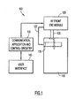
- FIG. 1 is a schematic block diagram of an example mobile communication device by which the present general inventive concept may be embodied.
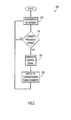
- FIG. 2 is a flow diagram of an example tuning method for a slot antenna embodying the present general inventive concept
- FIG. 3A is a diagram of an example slot antenna by which the present general inventive concept may be embodied.
- FIG. 3B is a diagram illustrating details of the slot antenna of FIG. 3A .
- FIG. 4 is a schematic block diagram of an example antenna tuning circuit by which the present general inventive concept may be embodied.
- FIGs.5A-5C are graphs depicting electrical characteristics of a particular slot antenna embodying the present general inventive concept.
- exemplary is used herein to mean, "serving as an example, instance or illustration.” Any embodiment of construction, process, design, technique, etc., designated herein as exemplary is not necessarily to be construed as preferred or advantageous over other such embodiments.
- FIG. 1 is a schematic block diagram of an exemplary mobile communication device 100, which may be, for example, an LTE-compliant mobile device.
- Mobile device 100 may include an antenna 110 that radiates and intercepts electromagnetic energy at a selected carrier frequency.
- Antenna 110 may be coupled to a radio-frequency (RF) front end module (FEM) 120 through a suitable transmission line connection 125.
- RF FEM 130 may convey communication data to and from suitable communication, application and control circuitry 130, which is, in turn, conveyed to and from antenna 110.
- Received communication data and communication data for transmission may be presented to and provided by user interface 140, by which a user interacts with other devices over a communication network and controls features of mobile device 100.
- RF radio-frequency
- antenna 110 may be an open-end slot antenna having a tuning circuit 115, by which the resonant frequency of antenna 110 is modified to match a frequency band selected from a plurality of frequency bands for which mobile device 100 is designed.
- RF FEM 120 generates a control signal 127 in accordance with a selected carrier frequency. While control signal 127 is illustrated as being provided by RF FEM 120, the present invention is not so limited. Control signal 127 is provided to tuning circuit 115 in accordance with the selected carrier frequency, such as that in a band specified by a particular standard or protocol, such as the E-UTRAN radio access standard.
- Tuning the antenna 100 may be performed via exemplary process 200 illustrated in FIG. 2 .
- operation 205 communications occur over antenna 110 in a particular band of frequencies.
- antenna 110 is tuned by tuning circuit 115 to resonate at a resonant frequency in the currently selected frequency band.
- tuning may be achieved through a resonant circuit selected from a plurality of such circuits.
- the term resonant circuit refers to a combination of circuit elements selected by tuning circuit 115 and the characteristic impedance of antenna 110.
- embodiments of the invention may include detection circuitry that detects a change in communication requirements and/or enforced standards in the performance of operation 210.
- a user of mobile device 100 may manually switch the device into another operational mode, such as through suitable controls on user interface 140.
- the present invention is not limited to the manner in which embodiments of the present invention determine the requirement for changing communication parameters, such as the carrier frequency and/or operational frequency bands.
- control signal 127 is generated in operation 215 and provided to tuning circuit 115, by which the appropriate tuning circuitry is engaged in operation 220.
- Process 200 may then transition to operation 205, in which mobile device 100 communicates through the network at the selected carrier frequency.
- FIG. 3A illustrates an exemplary antenna 300 consistent with the present invention.
- antenna 300 is a slot antenna comprising an open slot radiator 330, which may be referred to simply as slot 330, and a tuning circuit 320 to control the resonant mode of antenna 300.
- Slot 330 may be formed in a planar conductor 310, such as copper, disposed on a planar dielectric substrate 315, such as an FR-4 glass-reinforced epoxy laminate.
- antenna 300 may be described herein as comprising a conductor side 340 and a substrate side 350.
- Conductor 310 may be held at ground equipotential and, as such, may be referred to herein as ground plane 310.
- Conductor 310 and substrate 315 may be equally sized into a rectangular shape of longitudinal dimension X and lateral dimension Y.
- the position of slot 330, illustrated in FIG. 3A as distance X' measured from midline 345, will vary by application and may be constrained by other design factors, such as placement of other circuitry or mechanical structure in mobile device 100.
- a grounding strap 325 may be positioned between slot 330 and the nearest lateral edge of ground plane 310.
- ground strap 325 may be elevated by a distance Z from the surface of ground plane 310 and may be electrically connected to ground plane 310 at predetermined grounding points 323 and 327. The elevation distance Z will vary by application, e.g., by the wavelength in the corresponding frequency bands and the location X' of slot 300.
- antenna 300 is excited by an electromagnetic signal on feed line 335, where such electromagnetic signal may be provided to feed line 335 on transmission line 125 illustrated in FIG. 1 .
- Feed line 355 may be a microstrip transmission line formed on substrate side 350 and terminated at ground conductor 310, such as via a through-hole from substrate side 350 to conductor side 340, by ground connection 337.
- ground conductor 310 such as via a through-hole from substrate side 350 to conductor side 340, by ground connection 337.
- FIG. 3B illustrates slot 330 in more detail.
- Slot 330 is formed in ground plane 310 to expose the dielectric substrate 315 and includes an open end 334 and a closed end 336.
- the length L of slot 330 is one-quarter wavelength ( ⁇ e /4), where ⁇ e is an effective wavelength of the carrier signal taking into account the permittivity of dielectric substrate 315.
- ⁇ e is an effective wavelength of the carrier signal taking into account the permittivity of dielectric substrate 315.
- ⁇ e 0.468* ⁇ 0
- ⁇ 0 is the free-space wavelength of the carrier signal.
- ⁇ e is a design parameter that may be selected in accordance with the tunable range of slot 300.
- the width W of slot 330 is another such design parameter, while the distance D of slot 300 from the nearest lateral edge 312 of conductor 310 may be constrained by mechanical requirements in mobile device 100, as discussed above with reference to the distance X' in FIG. 3A .
- Tuning circuit 320 may be positioned at the open end 334 of slot 330 and contained in a single region of length L' and width W + W'. That is, the tuning circuit does not extend into slot 330 beyond the containing L' by (W + W') region.
- Tuning circuit 320 may include an RF switch 365 and one or more tuning elements 364a-364n. The conductive path through RF switch 365 may be selected by one or more control signals 127 provided to one or more position selection terminals, representatively illustrated at position selection terminal 366.
- RF switch 365 may include a common terminal 367 electrically connected to ground plane 310 and a plurality of switched terminals 369a-369n electrically connected to tuning circuit elements 361a-361n, which, in turn, are series connected to ground plane 310.
- FIG. 4 is a schematic block diagram of an exemplary tuning circuit 420 comprising RF switch 465 and tuning elements 464a-464n, representatively referred to herein as tuning element(s) 464.
- Tuning elements 464 may be individual discrete circuit components, such as, but not limited to, capacitors and inductors, or may be combinations of such circuit components that form individual tuning circuits. The ordinarily skilled artisan will recognize numerous implementations of tuning elements 464 that may be used without departing from the spirit and intended scope of the present invention.
- common terminal 467 of switch 465 may be electrically connected to ground plane 410 and switched terminals 469a-469n, representatively referred to herein as switched terminal(s) 469, may be series connected to respective tuning elements 464, which are each terminated at ground plane 410.
- Each tuning element 464 may be configured to tune a resonant frequency of slot 330 to a corresponding target frequency, such as a prescribed carrier frequency in a communication frequency band, such as an e-UTRA band for a particular geographic region.
- target frequency such as a prescribed carrier frequency in a communication frequency band, such as an e-UTRA band for a particular geographic region.
- slot 330 may be designed and constructed for a fixed operating frequency, which is then tuned for other operating frequencies by switching contacts 461 into a position that selects the appropriate tuning element 464.
- one of tuning elements 464 is an open circuit, as illustrated at position 362 in FIG. 3B , so that the operating frequency for which slot 330 is fixed may be selected as one of the target frequencies.
- slot 330 may be designed to correspond to, for example, the frequency carrier of a particular home geographical region, and tuning elements 464 may be selected to tune the resonant frequency of slot 330 to accommodate carrier frequencies in other geographical regions.
- a control signal such as control signal 127
- tuning circuit control terminal 405 Upon a determination that antenna 300 is to be tuned to a particular frequency, a control signal, such as control signal 127, may be applied to tuning circuit control terminal 405 and a corresponding signal may be applied to position selection terminal 466 of RF switch 465.
- a conductive path representatively illustrated by contact 461, is formed through the appropriate tuning element 464 to ground plane 410.
- RF switch 465 is illustrated as a mechanical single-pole, multiple-throw switch, such is solely for purposes of description. As such, RF switch 465 may not have contacts, per se, but rather semiconductors, such as PIN diodes or the like, to form the conductive path.
- the present invention is not limited to a particular implementation of RF switch 465 and, in a typical implementation, will be a solid state RF switch.
- Region 338 is characterized by a broadening of slot 300 by a distance W' over a length L'.
- portions of tuning circuit 320 may be contained in the L' by W' region 338 without extending into the remaining width W of slot 330 to minimize the impact of the tuning circuit 320 on the operation of antenna 300.
- relatively large electrical components of tuning circuit 320 such as RF switch 365, may be contained in region 338 while relatively smaller components, such as small surface mounted capacitors and inductors, may reside in slot 330.
- FIGS. 5A-5C are graphs depicting performance of a specific implementation of antenna 300.
- the exemplary mobile device antenna is tunable forGSM850/900dual-band operation and GSM1800/1900/UMTS triple-band operation in one state of tuning circuit 320 and is tunable for LTE700 band operation in another state of tuning circuit 320.
- tuning element 1 corresponding to tuning circuit State I may be an open circuit and tuning element 2 corresponding to tuning circuit State II may be a 0.7 pF capacitor.
- FIG. 5A is a graph of simulated return loss for the exemplary internal mobile device tunable antenna per the design described above and FIG. 5B is a graph of measured results of the same design.
- the antenna's lower band impedance bandwidth encompasses GSM850/900 dual-band frequencies and the antenna's upper band impedance bandwidth encompasses GSM1800/1900/UMTS triple-band frequencies.
- the antenna's lower band resonant mode is shifted to a lower frequency, i.e., about 700 - 800 MHz.
- the antenna's lower band impedance bandwidth encompasses LTE700 frequencies.
- the measured antenna efficiency which includes the impedance mismatch loss for the exemplary tunable antenna is illustrated in FIG. 5C .
- the measured efficiency is 71% - 80% and 25% - 35%, respectively, which are acceptable for practical applications.
Landscapes
- Engineering & Computer Science (AREA)
- Computer Networks & Wireless Communication (AREA)
- Waveguide Aerials (AREA)
- Support Of Aerials (AREA)
Abstract
An open slot antenna is formed in a planar conductor (310) on a dielectric substrate (315). A tuning circuit (320) is disposed toward an open end of the slot antenna (330) and is used to select a resonant frequency of the antenna by electrically connecting one of multiple tuning elements across opposing sides of the slot. The tunable antenna so constructed may be incorporated into a handheld mobile communication device that can be operated in different geographic regions, each having different regional communication standards under which mobile communications are conducted.
Description
- This patent application claims priority under 35 USC §119 of Taiwan R.O.C. Patent Application No.
101107827 filed March 8, 2012 - The present disclosure relates to mobile wireless communication device antennas.
- Long Term Evolution(LTE) handheld communication devices continue to be developed with trends toward smaller devices and wider band width operation. Size limitations of thin mobile devices present challenges for internal antenna design in LTE/2G/3Gwideband operations. Operating a single device at different locations with distinct regionally-enforced communication standards presents additional challenges. This is clear from Table I, which illustrates possible LTE band distributions for the Evolved UMTS (Universal Mobile Telecommunications System)Terrestrial Radio Access (e-UTRA) radio access standard used in various geographical regions.
TABLE 1 e-UTRA Duplex Mode Uplink Freq. Range Downlink Freq. Range Band IV FDD 1710-1755 (MHz) 2110-2155 (MHz) Band XIII FDD 777-787 746-756 Band XVII FDD 704-716 734-746 Band XX FDD 832-862 791-821 Band XXXVIII TDD 2570-2620 Band XL TDD 2300-2400 - Slot antennas provide simple radiating structures for use in such mobile devices and various technologies for tuning slot antennas exist. For example,
US Patent 7,176,842 entitled Dual Band Slot Antenna incorporates electronic components prudently distributed across the antenna slot to shunt the slot at certain locations, thereby changing the antenna's effective length.US Patent Application Publication 2005/0174294 entitled Switchable Slot Antenna discloses another technique by which the effective length of the antenna is changed by solid state shunt switches distributed across the slot antenna. Both of these techniques rely on the distribution of switches across the radiating slot, each of which requires its own control signals, e.g., bias voltages. The distributed nature of the tuning circuits of these antennas increases the size of the overall circuit. Moreover, both of the afore-referenced systems utilize a half wavelength slot, which imposes mechanical limitations on the antenna and, thereby, on the size of the mobile device. The need for smaller tunable antennas for mobile communication devices continues to be felt. - The present general inventive concept is directed to an antenna comprising a slot radiator formed in a planar conductor and having an open and a closed end. A tuning circuit is used to select a resonant frequency of the antenna. The tuning circuit is electrically coupled to the planar conductor at opposing sides of the open end of the slot and is configured to select a circuit path from a plurality of circuit paths. The tuning circuit may include a switch circuit andone or more sets of circuit elements including, for example, a capacitor, connected between the switch circuit and the slot. The circuit paths connect respective sets of circuit elements through the switch circuit to the opposing sides of the planar conductor.
-
FIG. 1 is a schematic block diagram of an example mobile communication device by which the present general inventive concept may be embodied. -
FIG. 2 is a flow diagram of an example tuning method for a slot antenna embodying the present general inventive concept -
FIG. 3A is a diagram of an example slot antenna by which the present general inventive concept may be embodied. -
FIG. 3B is a diagram illustrating details of the slot antenna ofFIG. 3A . -
FIG. 4 is a schematic block diagram of an example antenna tuning circuit by which the present general inventive concept may be embodied. -
FIGs.5A-5C are graphs depicting electrical characteristics of a particular slot antenna embodying the present general inventive concept. - The present inventive concept is best described through certain embodiments thereof, which are described in detail herein with reference to the accompanying drawings, wherein like reference numerals refer to like features throughout. It is to be understood that the term invention, when used herein, is intended to connote the inventive concept underlying the embodiments described below and not merely the embodiments themselves. It is to be understood further that the general inventive concept is not limited to the illustrative embodiments described below and the following descriptions should be read in such light.
- Additionally, the word exemplary is used herein to mean, "serving as an example, instance or illustration." Any embodiment of construction, process, design, technique, etc., designated herein as exemplary is not necessarily to be construed as preferred or advantageous over other such embodiments.
-
FIG. 1 is a schematic block diagram of an exemplarymobile communication device 100, which may be, for example, an LTE-compliant mobile device.Mobile device 100 may include anantenna 110 that radiates and intercepts electromagnetic energy at a selected carrier frequency.Antenna 110 may be coupled to a radio-frequency (RF) front end module (FEM) 120 through a suitabletransmission line connection 125. RF FEM 130 may convey communication data to and from suitable communication, application andcontrol circuitry 130, which is, in turn, conveyed to and fromantenna 110. Received communication data and communication data for transmission may be presented to and provided byuser interface 140, by which a user interacts with other devices over a communication network and controls features ofmobile device 100. - As will be described in more detail below,
antenna 110 may be an open-end slot antenna having atuning circuit 115, by which the resonant frequency ofantenna 110 is modified to match a frequency band selected from a plurality of frequency bands for whichmobile device 100 is designed. In certain embodiments, RF FEM 120 generates acontrol signal 127 in accordance with a selected carrier frequency. Whilecontrol signal 127 is illustrated as being provided by RF FEM 120, the present invention is not so limited.Control signal 127 is provided totuning circuit 115 in accordance with the selected carrier frequency, such as that in a band specified by a particular standard or protocol, such as the E-UTRAN radio access standard. - Tuning the
antenna 100 may be performed viaexemplary process 200 illustrated inFIG. 2 . Inoperation 205, communications occur overantenna 110 in a particular band of frequencies. In this arbitrary initial state,antenna 110 is tuned bytuning circuit 115 to resonate at a resonant frequency in the currently selected frequency band. Such tuning may be achieved through a resonant circuit selected from a plurality of such circuits. It is to be understood that the term resonant circuit refers to a combination of circuit elements selected bytuning circuit 115 and the characteristic impedance ofantenna 110. Inoperation 210 it is determined whether a change in carrier frequency is required for proper communication over a particular network. In certain instances, such frequency change is necessary to comply with regionally- and/or carrier-enforced communication standards. Accordingly, embodiments of the invention may include detection circuitry that detects a change in communication requirements and/or enforced standards in the performance ofoperation 210. Optionally or additionally, a user ofmobile device 100 may manually switch the device into another operational mode, such as through suitable controls onuser interface 140. The present invention is not limited to the manner in which embodiments of the present invention determine the requirement for changing communication parameters, such as the carrier frequency and/or operational frequency bands. - If it is determined in
operation 210 that no change in carrier frequency is necessary, operation ofmobile device 100 continues in the current operational mode inoperation 205. If, however, it is determined that a change in carrier frequency is appropriate,control signal 127 is generated inoperation 215 and provided totuning circuit 115, by which the appropriate tuning circuitry is engaged inoperation 220.Process 200 may then transition tooperation 205, in whichmobile device 100 communicates through the network at the selected carrier frequency. -
FIG. 3A illustrates anexemplary antenna 300 consistent with the present invention. As illustrated in the figure,antenna 300 is a slot antenna comprising anopen slot radiator 330, which may be referred to simply asslot 330, and atuning circuit 320 to control the resonant mode ofantenna 300.Slot 330 may be formed in aplanar conductor 310, such as copper, disposed on a planardielectric substrate 315, such as an FR-4 glass-reinforced epoxy laminate. Accordingly,antenna 300 may be described herein as comprising aconductor side 340 and asubstrate side 350.Conductor 310 may be held at ground equipotential and, as such, may be referred to herein asground plane 310.Conductor 310 andsubstrate 315 may be equally sized into a rectangular shape of longitudinal dimension X and lateral dimension Y. The position ofslot 330, illustrated inFIG. 3A as distance X' measured frommidline 345, will vary by application and may be constrained by other design factors, such as placement of other circuitry or mechanical structure inmobile device 100. To facilitate impedance matching in lower frequency bands to whichantenna 300 may be tuned, a groundingstrap 325 may be positioned betweenslot 330 and the nearest lateral edge ofground plane 310. In certain embodiments,ground strap 325 may be elevated by a distance Z from the surface ofground plane 310 and may be electrically connected toground plane 310 atpredetermined grounding points 323 and 327. The elevation distance Z will vary by application, e.g., by the wavelength in the corresponding frequency bands and the location X' ofslot 300. - As illustrated in
FIG. 3A ,antenna 300 is excited by an electromagnetic signal on feed line 335, where such electromagnetic signal may be provided to feed line 335 ontransmission line 125 illustrated inFIG. 1 .Feed line 355 may be a microstrip transmission line formed onsubstrate side 350 and terminated atground conductor 310, such as via a through-hole fromsubstrate side 350 toconductor side 340, byground connection 337. The ordinarily skilled artisan will recognize various transmission line design techniques that may be used in conjunction with the present invention to ensure thatfeed line 355 is impedance-matched totransmission line 125 and to slot 330, and is positioned to properly exciteslot 330 for radiating electromagnetic signals. -
FIG. 3B illustratesslot 330 in more detail.Slot 330 is formed inground plane 310 to expose thedielectric substrate 315 and includes anopen end 334 and aclosed end 336. The length L ofslot 330 is one-quarter wavelength (λ e /4), where λ e is an effective wavelength of the carrier signal taking into account the permittivity ofdielectric substrate 315. For an FR-4 substrate, for example, λ e = 0.468*λ 0 , where λ 0 is the free-space wavelength of the carrier signal. In certain embodiments, λ e is a design parameter that may be selected in accordance with the tunable range ofslot 300. The width W ofslot 330 is another such design parameter, while the distance D ofslot 300 from the nearest lateral edge 312 ofconductor 310 may be constrained by mechanical requirements inmobile device 100, as discussed above with reference to the distance X' inFIG. 3A . -
Tuning circuit 320 may be positioned at theopen end 334 ofslot 330 and contained in a single region of length L' and width W + W'. That is, the tuning circuit does not extend intoslot 330 beyond the containing L' by (W + W') region.Tuning circuit 320 may include anRF switch 365 and one ormore tuning elements 364a-364n. The conductive path throughRF switch 365 may be selected by one or more control signals 127 provided to one or more position selection terminals, representatively illustrated atposition selection terminal 366.RF switch 365 may include acommon terminal 367 electrically connected toground plane 310 and a plurality of switchedterminals 369a-369n electrically connected to tuning circuit elements 361a-361n, which, in turn, are series connected toground plane 310. -
FIG. 4 is a schematic block diagram of anexemplary tuning circuit 420 comprisingRF switch 465 andtuning elements 464a-464n, representatively referred to herein as tuning element(s) 464. Tuning elements 464 may be individual discrete circuit components, such as, but not limited to, capacitors and inductors, or may be combinations of such circuit components that form individual tuning circuits. The ordinarily skilled artisan will recognize numerous implementations of tuning elements 464 that may be used without departing from the spirit and intended scope of the present invention. - As described with respect to
FIG. 3B ,common terminal 467 ofswitch 465 may be electrically connected toground plane 410 and switchedterminals 469a-469n, representatively referred to herein as switched terminal(s) 469, may be series connected to respective tuning elements 464, which are each terminated atground plane 410. Each tuning element 464 may be configured to tune a resonant frequency ofslot 330 to a corresponding target frequency, such as a prescribed carrier frequency in a communication frequency band, such as an e-UTRA band for a particular geographic region. Accordingly, slot 330 may be designed and constructed for a fixed operating frequency, which is then tuned for other operating frequencies by switchingcontacts 461 into a position that selects the appropriate tuning element 464. In certain embodiments, one of tuning elements 464 is an open circuit, as illustrated atposition 362 inFIG. 3B , so that the operating frequency for whichslot 330 is fixed may be selected as one of the target frequencies. When so embodied,slot 330 may be designed to correspond to, for example, the frequency carrier of a particular home geographical region, and tuning elements 464 may be selected to tune the resonant frequency ofslot 330 to accommodate carrier frequencies in other geographical regions. - Upon a determination that
antenna 300 is to be tuned to a particular frequency, a control signal, such ascontrol signal 127, may be applied to tuningcircuit control terminal 405 and a corresponding signal may be applied toposition selection terminal 466 ofRF switch 465. In response to the control signal, a conductive path, representatively illustrated bycontact 461, is formed through the appropriate tuning element 464 toground plane 410. It is to be understood that whileRF switch 465 is illustrated as a mechanical single-pole, multiple-throw switch, such is solely for purposes of description. As such,RF switch 465 may not have contacts, per se, but rather semiconductors, such as PIN diodes or the like, to form the conductive path. The present invention is not limited to a particular implementation ofRF switch 465 and, in a typical implementation, will be a solid state RF switch. - Returning to
FIG. 3B , there is illustrated aregion 338 at theopen end 334 ofslot 330.Region 338 is characterized by a broadening ofslot 300 by a distance W' over a length L'. When the present invention is so embodied, portions of tuningcircuit 320 may be contained in the L' by W'region 338 without extending into the remaining width W ofslot 330 to minimize the impact of thetuning circuit 320 on the operation ofantenna 300. For example, relatively large electrical components oftuning circuit 320, such asRF switch 365, may be contained inregion 338 while relatively smaller components, such as small surface mounted capacitors and inductors, may reside inslot 330. In other embodiments, all circuit components other than conductive traces connecting tuning elements 364 toground plane 310 are contained in broadenedregion 338. If the region defined in the L' by (W + W') rectangle in which tuning circuit 320is contained is kept small with respect to wavelengthλ0, e.g., L' = λ0/40, the impact on the operation ofantenna 300 is minimal and can be compensated for by, for example, suitably selecting tuning elements 364 to account for such impact. -
FIGS. 5A-5C are graphs depicting performance of a specific implementation ofantenna 300. In the example embodiment,antenna 300 is designed around a 900 MHz carrier frequency (λ0= 333mm, λe = 153mm) and designed to be used as an internal antenna of a handheld mobile communication device. Using the dimensions illustrated inFIGs. 3A and3B , the internal mobile device antenna is sized to the following: lateral dimension X = 60mm (0.18*λ0= 0.4*λe), longitudinal dimension Y = 110mm (0.33*λ0= 0.7*λe), slot length L = 39mm (0.12*λ0= 0.25*λe), slot width W = 4mm (0.012 λ0= 0.03*λe), offset from nearest lateral edge D = 6mm (0.018*λ0= 0.04*λe) and ground strap elevation height Z = 5mm (0.015*λ0= 0.032*λe). The exemplary mobile device antenna is tunable forGSM850/900dual-band operation and GSM1800/1900/UMTS triple-band operation in one state of tuningcircuit 320 and is tunable for LTE700 band operation in another state of tuningcircuit 320. Accordingly, tuningelement 1 corresponding to tuning circuit State I may be an open circuit andtuning element 2 corresponding to tuning circuit State II may be a 0.7 pF capacitor. -
FIG. 5A is a graph of simulated return loss for the exemplary internal mobile device tunable antenna per the design described above andFIG. 5B is a graph of measured results of the same design. As illustrated in the figures, when the tuning circuit is in State I, the antenna's lower band impedance bandwidth encompasses GSM850/900 dual-band frequencies and the antenna's upper band impedance bandwidth encompasses GSM1800/1900/UMTS triple-band frequencies. In State II of the tuning circuit(C= 0.7 pF), the antenna's lower band resonant mode is shifted to a lower frequency, i.e., about 700 - 800 MHz. In this state, the antenna's lower band impedance bandwidth encompasses LTE700 frequencies. It is to be noted that the simulation results illustrated inFIG. 5A and the actual measurements illustrated inFIG. 5B are in reasonable agreement. The measured antenna efficiency, which includes the impedance mismatch loss for the exemplary tunable antenna is illustrated inFIG. 5C . Over the desired GSM850/900 (State I, Open Circuit) and LTE700 (State II, C = 0.7 pF) bands, the measured efficiency is 71% - 80% and 25% - 35%, respectively, which are acceptable for practical applications. - The descriptions above are intended to illustrate possible implementations of the present inventive concept and are not restrictive. Many variations, modifications and alternatives will become apparent to the skilled artisan upon review of this disclosure. For example, components equivalent to those shown and described may be substituted therefore, elements and methods individually described may be combined, and elements described as discrete may be distributed across many components. The scope of the invention should therefore be determined not with reference to the description above, but with reference to the appended claims, along with their full range of equivalents.
Claims (15)
- An apparatus comprising:an antenna comprising a slot radiator formed in a planar conductor and having an open and a closed end; anda tuning circuit by which a resonant frequency of the antenna is selected, the tuning circuit being electrically coupled to the planar conductor at opposing sides of the slot and configured to select a circuit path from a plurality of circuit paths.
- The apparatus of claim 1, wherein the tuning circuit is contained in a single region at the open end of the slot.
- The apparatus of claim 2, wherein the tuning circuit comprises:a switch circuit including a control terminal by which a contact position of the switch is selected; andat least one circuit element connected between the switch circuit and the slot, wherein the circuit paths in the containing region connect the circuit element through the switch circuit to the opposing sides of the planar conductor.
- The apparatus of claim 3, wherein the containing region at the open end of the slot comprises a broadened region that is wider than the closed end of the slot and the switch circuit is located entirely in the broadened region.
- The apparatus of claim 3, wherein the at least one circuit element comprises a plurality of circuit elements connected between the switch circuit and the slot and the circuit paths in the containing region connect a selected one of the circuit elements through the switch circuit to the opposing sides of the planar conductor.
- The apparatus of claim 5, wherein the circuit elements include respective capacitors having a capacitance that is other than the capacitance of the capacitor in another of the sets of circuit elements.
- The apparatus of claim 3, wherein the tuning circuit includes an open circuit selectable by the switch.
- The apparatus of claim 1, wherein the antenna comprises:a dielectric substrate on which the planar conductor is disposed, wherein the slot is formed in the conductor to expose the substrate and the open end of the slot is formed at an edge of the planar conductor and an edge of the substrate.
- The apparatus of claim 8, wherein the slot is closer to one lateral edge of the planar conductor than to another lateral edge of the planar conductor.
- The apparatus of claim 9 further comprising:a grounding strap between the slot and a nearest lateral edge of the planar conductor parallel with the slot, wherein the grounding strap is electrically connected to the planar conductor.
- The apparatus of claim 1, wherein the slot is a quarter-wavelength slot corresponding to a fixed resonant frequency.
- A method comprising:determining a frequency band of operation of a communication device;selecting a tuning circuit for an open slot antenna from a plurality of tuning circuits in accordance with an antenna resonant frequency corresponding to the frequency band, wherein the plurality of tuning circuits are located in a single confined region in a radiating slot of the slot antenna; andcommunicating via the slot antenna at a frequency in the frequency band.
- The method of claim 12, further comprising:determining that the frequency of operation has changed;selecting another tuning circuit from the plurality of tuning circuits; andcommunicating via the slot antenna at a changed frequency.
- The method of claim 13, wherein determining that the communication frequency has changed includes:determining whether the communication circuit is relocated from one region corresponding to one band of communication frequencies to another region corresponding to another band of communication frequencies.
- The method of claim 14, wherein determining that the communication frequency has changed includes:determining whether a user of the communication circuit has selected, by way of a user control, a band of communication frequencies from a plurality of bands of frequencies.
Applications Claiming Priority (1)
| Application Number | Priority Date | Filing Date | Title |
|---|---|---|---|
| TW101107827A TWI539673B (en) | 2012-03-08 | 2012-03-08 | Adjustable slot antenna |
Publications (1)
| Publication Number | Publication Date |
|---|---|
| EP2637249A1 true EP2637249A1 (en) | 2013-09-11 |
Family
ID=47257485
Family Applications (1)
| Application Number | Title | Priority Date | Filing Date |
|---|---|---|---|
| EP12192447.6A Withdrawn EP2637249A1 (en) | 2012-03-08 | 2012-11-13 | Tunable slot antenna |
Country Status (3)
| Country | Link |
|---|---|
| US (1) | US9356356B2 (en) |
| EP (1) | EP2637249A1 (en) |
| TW (1) | TWI539673B (en) |
Cited By (2)
| Publication number | Priority date | Publication date | Assignee | Title |
|---|---|---|---|---|
| RU176019U1 (en) * | 2017-02-15 | 2017-12-26 | Акционерное общество "Центральный научно-исследовательский институт "Курс" (АО "ЦНИИ "Курс") | CONSTRUCTION OF A WAVEGUIDE-SLOT ANTENNA ARRAY WITH PIN-CONTROLLED DIAGRAM DIRECTION DIAGRAM |
| CN108459660A (en) * | 2017-02-17 | 2018-08-28 | 和硕联合科技股份有限公司 | Electronic device |
Families Citing this family (31)
| Publication number | Priority date | Publication date | Assignee | Title |
|---|---|---|---|---|
| CN109998483B (en) * | 2013-09-16 | 2023-02-28 | 斯坦福大学董事会 | Multi-element coupler for electromagnetic energy generation |
| US20150116161A1 (en) * | 2013-10-28 | 2015-04-30 | Skycross, Inc. | Antenna structures and methods thereof for determining a frequency offset based on a signal magnitude measurement |
| KR102166351B1 (en) | 2014-01-29 | 2020-10-15 | 삼성전자주식회사 | Communication method and apparatus |
| GB2533339A (en) * | 2014-12-17 | 2016-06-22 | Vertu Corp Ltd | Multiband slot antenna system and apparatus |
| KR102397407B1 (en) * | 2015-02-27 | 2022-05-13 | 삼성전자주식회사 | Antenna device and electronic device with the same |
| WO2016187886A1 (en) * | 2015-05-28 | 2016-12-01 | 华为技术有限公司 | Slot antenna and electronic device |
| TWI569512B (en) * | 2015-11-18 | 2017-02-01 | 廣達電腦股份有限公司 | Mobile device |
| US10290946B2 (en) * | 2016-09-23 | 2019-05-14 | Apple Inc. | Hybrid electronic device antennas having parasitic resonating elements |
| TWI732931B (en) * | 2016-09-29 | 2021-07-11 | 仁寶電腦工業股份有限公司 | Antenna structure |
| KR102396315B1 (en) | 2017-08-21 | 2022-05-10 | 삼성전자주식회사 | Antenna device and electronic device including the same |
| US10333217B1 (en) | 2018-01-12 | 2019-06-25 | Pivotal Commware, Inc. | Composite beam forming with multiple instances of holographic metasurface antennas |
| US10225760B1 (en) | 2018-03-19 | 2019-03-05 | Pivotal Commware, Inc. | Employing correlation measurements to remotely evaluate beam forming antennas |
| CN111903063B (en) | 2018-03-19 | 2022-08-12 | 皮沃塔尔卡姆瓦雷股份有限公司 | Transmit wireless signals through physical barriers |
| CN108899642A (en) * | 2018-06-12 | 2018-11-27 | 瑞声科技(新加坡)有限公司 | The mobile terminal of antenna system and the application antenna system |
| US10862545B2 (en) | 2018-07-30 | 2020-12-08 | Pivotal Commware, Inc. | Distributed antenna networks for wireless communication by wireless devices |
| US10326203B1 (en) | 2018-09-19 | 2019-06-18 | Pivotal Commware, Inc. | Surface scattering antenna systems with reflector or lens |
| US10522897B1 (en) | 2019-02-05 | 2019-12-31 | Pivotal Commware, Inc. | Thermal compensation for a holographic beam forming antenna |
| US10468767B1 (en) | 2019-02-20 | 2019-11-05 | Pivotal Commware, Inc. | Switchable patch antenna |
| CN114586239A (en) * | 2019-11-01 | 2022-06-03 | 惠普发展公司,有限责任合伙企业 | Antenna assembly with resonant circuit spanning ground plane slot |
| TWI719707B (en) | 2019-11-11 | 2021-02-21 | 啓碁科技股份有限公司 | Antenna structure |
| US10734736B1 (en) | 2020-01-03 | 2020-08-04 | Pivotal Commware, Inc. | Dual polarization patch antenna system |
| US11069975B1 (en) | 2020-04-13 | 2021-07-20 | Pivotal Commware, Inc. | Aimable beam antenna system |
| KR102872581B1 (en) | 2020-05-27 | 2025-10-17 | 피보탈 컴웨어 인코포레이티드 | RF signal repeater device management for 5G wireless networks |
| US11026055B1 (en) | 2020-08-03 | 2021-06-01 | Pivotal Commware, Inc. | Wireless communication network management for user devices based on real time mapping |
| WO2022056024A1 (en) | 2020-09-08 | 2022-03-17 | Pivotal Commware, Inc. | Installation and activation of rf communication devices for wireless networks |
| AU2022208705A1 (en) | 2021-01-15 | 2023-08-31 | Pivotal Commware, Inc. | Installation of repeaters for a millimeter wave communications network |
| EP4285628A4 (en) | 2021-01-26 | 2024-12-18 | Pivotal Commware, Inc. | INTELLIGENT REPEATER SYSTEMS |
| US11451287B1 (en) | 2021-03-16 | 2022-09-20 | Pivotal Commware, Inc. | Multipath filtering for wireless RF signals |
| AU2022307056A1 (en) | 2021-07-07 | 2024-02-15 | Pivotal Commware, Inc. | Multipath repeater systems |
| WO2023076405A1 (en) | 2021-10-26 | 2023-05-04 | Pivotal Commware, Inc. | Rf absorbing structures |
| JP2025512562A (en) | 2022-04-18 | 2025-04-17 | ピヴォタル コムウェア インコーポレイテッド | Time division duplex repeater timing recovery with global positioning satellite system |
Citations (8)
| Publication number | Priority date | Publication date | Assignee | Title |
|---|---|---|---|---|
| DE3246365A1 (en) * | 1982-12-15 | 1984-06-20 | Philips Patentverwaltung Gmbh, 2000 Hamburg | Notch antenna for a wide frequency band |
| EP1280226A1 (en) * | 2000-04-20 | 2003-01-29 | Mitsubishi Denki Kabushiki Kaisha | Portable radio device |
| US20030122721A1 (en) * | 2001-12-27 | 2003-07-03 | Hrl Laboratories, Llc | RF MEMs-tuned slot antenna and a method of making same |
| EP1437794A1 (en) * | 2003-01-08 | 2004-07-14 | Sony Ericsson Mobile Communications Japan, Inc. | Radio device with a notch antenna |
| US20050174294A1 (en) | 2002-05-31 | 2005-08-11 | The Regents Of The University Of Michigan | Switchable slot antenna |
| WO2006114477A1 (en) * | 2005-04-28 | 2006-11-02 | Pulse Finland Oy | Slot antenna |
| US7176842B2 (en) | 2004-10-27 | 2007-02-13 | Intel Corporation | Dual band slot antenna |
| WO2007023442A2 (en) * | 2005-08-24 | 2007-03-01 | Koninklijke Philips Electronics N.V. | Device comprising an antenna for exchanging radio frequency signals |
Family Cites Families (11)
| Publication number | Priority date | Publication date | Assignee | Title |
|---|---|---|---|---|
| US4893131A (en) | 1988-06-15 | 1990-01-09 | Smith William J | Mobile or ground mounted arcuate antenna |
| US6043786A (en) * | 1997-05-09 | 2000-03-28 | Motorola, Inc. | Multi-band slot antenna structure and method |
| FR2819109A1 (en) * | 2001-01-04 | 2002-07-05 | Cit Alcatel | MULTI-BAND ANTENNA FOR MOBILE DEVICES |
| DE60223515T2 (en) * | 2001-03-15 | 2008-09-18 | Matsushita Electric Industrial Co., Ltd., Kadoma | ANTENNA DEVICE |
| JP2004096341A (en) * | 2002-08-30 | 2004-03-25 | Fujitsu Ltd | Antenna device including inverted F-type antenna with variable resonance frequency |
| US7872605B2 (en) * | 2005-03-15 | 2011-01-18 | Fractus, S.A. | Slotted ground-plane used as a slot antenna or used for a PIFA antenna |
| JP2010062976A (en) * | 2008-09-05 | 2010-03-18 | Sony Ericsson Mobile Communications Ab | Notch antenna and wireless device |
| TWI393291B (en) | 2009-03-27 | 2013-04-11 | Acer Inc | A monopole slot antenna |
| FI20096134A0 (en) | 2009-11-03 | 2009-11-03 | Pulse Finland Oy | Adjustable antenna |
| US9472855B2 (en) * | 2012-02-23 | 2016-10-18 | Nec Corporation | Antenna device |
| US8884835B2 (en) * | 2012-08-09 | 2014-11-11 | Intel Mobile Communications GmbH | Antenna system, method and mobile communication device |
-
2012
- 2012-03-08 TW TW101107827A patent/TWI539673B/en active
- 2012-07-25 US US13/557,310 patent/US9356356B2/en active Active
- 2012-11-13 EP EP12192447.6A patent/EP2637249A1/en not_active Withdrawn
Patent Citations (8)
| Publication number | Priority date | Publication date | Assignee | Title |
|---|---|---|---|---|
| DE3246365A1 (en) * | 1982-12-15 | 1984-06-20 | Philips Patentverwaltung Gmbh, 2000 Hamburg | Notch antenna for a wide frequency band |
| EP1280226A1 (en) * | 2000-04-20 | 2003-01-29 | Mitsubishi Denki Kabushiki Kaisha | Portable radio device |
| US20030122721A1 (en) * | 2001-12-27 | 2003-07-03 | Hrl Laboratories, Llc | RF MEMs-tuned slot antenna and a method of making same |
| US20050174294A1 (en) | 2002-05-31 | 2005-08-11 | The Regents Of The University Of Michigan | Switchable slot antenna |
| EP1437794A1 (en) * | 2003-01-08 | 2004-07-14 | Sony Ericsson Mobile Communications Japan, Inc. | Radio device with a notch antenna |
| US7176842B2 (en) | 2004-10-27 | 2007-02-13 | Intel Corporation | Dual band slot antenna |
| WO2006114477A1 (en) * | 2005-04-28 | 2006-11-02 | Pulse Finland Oy | Slot antenna |
| WO2007023442A2 (en) * | 2005-08-24 | 2007-03-01 | Koninklijke Philips Electronics N.V. | Device comprising an antenna for exchanging radio frequency signals |
Non-Patent Citations (1)
| Title |
|---|
| SHIH-YUAN CHEN ET AL: "Frequency-agile, miniaturized slot antenna for hand-held devices", ELECTROMAGNETIC THEORY (EMTS), 2010 URSI INTERNATIONAL SYMPOSIUM ON, IEEE, PISCATAWAY, NJ, USA, 16 August 2010 (2010-08-16), pages 377 - 380, XP031802697, ISBN: 978-1-4244-5155-5 * |
Cited By (2)
| Publication number | Priority date | Publication date | Assignee | Title |
|---|---|---|---|---|
| RU176019U1 (en) * | 2017-02-15 | 2017-12-26 | Акционерное общество "Центральный научно-исследовательский институт "Курс" (АО "ЦНИИ "Курс") | CONSTRUCTION OF A WAVEGUIDE-SLOT ANTENNA ARRAY WITH PIN-CONTROLLED DIAGRAM DIRECTION DIAGRAM |
| CN108459660A (en) * | 2017-02-17 | 2018-08-28 | 和硕联合科技股份有限公司 | Electronic device |
Also Published As
| Publication number | Publication date |
|---|---|
| US9356356B2 (en) | 2016-05-31 |
| TWI539673B (en) | 2016-06-21 |
| US20130234901A1 (en) | 2013-09-12 |
| TW201338269A (en) | 2013-09-16 |
Similar Documents
| Publication | Publication Date | Title |
|---|---|---|
| US9356356B2 (en) | Tunable slot antenna | |
| EP2950387B1 (en) | Antennas with multiple feed circuits | |
| US6980154B2 (en) | Planar inverted F antennas including current nulls between feed and ground couplings and related communications devices | |
| US7187338B2 (en) | Antenna arrangement and module including the arrangement | |
| KR101088523B1 (en) | Wireless Terminals and Wireless Modules | |
| EP2608315B1 (en) | Switchable diversity antenna apparatus and methods | |
| EP1790034B1 (en) | Antenna device and portable radio communication device comprising such an antenna device | |
| US7889143B2 (en) | Multiband antenna system and methods | |
| KR100986702B1 (en) | Internal mimo antenna to selectively control isolation characteristic by isolation aid in multiband including lte band | |
| KR100666113B1 (en) | Internal Multi-Band Antenna with Multiple Layers | |
| US20130088404A1 (en) | Multi-feed antenna apparatus and methods | |
| US20140015719A1 (en) | Switched antenna apparatus and methods | |
| EP2348574B1 (en) | Antenna device | |
| US11417965B2 (en) | Planar inverted F-antenna integrated with ground plane frequency agile defected ground structure | |
| WO2008010149A1 (en) | Antenna with reduced sensitivity to user finger position | |
| US20160261050A1 (en) | Cognitive radio antenna assembly | |
| US20170271751A1 (en) | Cognitive radio antenna assembly | |
| US20090213026A1 (en) | Antenna arrangement provided with a wave trap | |
| CN1788390B (en) | Improvements in or relating to wireless terminals | |
| US7522936B2 (en) | Wireless terminal | |
| Yoon et al. | A frequency-selecting technique for mobile handset antennas based on capacitance switching | |
| KR101276649B1 (en) | Antenna device and wireless communication apparatus including the same | |
| KR20040004286A (en) | A Multi-Band Cable Antenna | |
| WO2008070373A1 (en) | Wideband antenna for mobile devices | |
| Ligthart et al. | Multi-band antennas with integrated circuitry in mobile phones |
Legal Events
| Date | Code | Title | Description |
|---|---|---|---|
| PUAI | Public reference made under article 153(3) epc to a published international application that has entered the european phase |
Free format text: ORIGINAL CODE: 0009012 |
|
| AK | Designated contracting states |
Kind code of ref document: A1 Designated state(s): AL AT BE BG CH CY CZ DE DK EE ES FI FR GB GR HR HU IE IS IT LI LT LU LV MC MK MT NL NO PL PT RO RS SE SI SK SM TR |
|
| AX | Request for extension of the european patent |
Extension state: BA ME |
|
| STAA | Information on the status of an ep patent application or granted ep patent |
Free format text: STATUS: THE APPLICATION IS DEEMED TO BE WITHDRAWN |
|
| 18D | Application deemed to be withdrawn |
Effective date: 20140312 |