EP2635031A2 - Systems and methods for image processing - Google Patents
Systems and methods for image processing Download PDFInfo
- Publication number
- EP2635031A2 EP2635031A2 EP13157208.3A EP13157208A EP2635031A2 EP 2635031 A2 EP2635031 A2 EP 2635031A2 EP 13157208 A EP13157208 A EP 13157208A EP 2635031 A2 EP2635031 A2 EP 2635031A2
- Authority
- EP
- European Patent Office
- Prior art keywords
- image data
- pixel
- horizontally
- pixels
- image
- Prior art date
- Legal status (The legal status is an assumption and is not a legal conclusion. Google has not performed a legal analysis and makes no representation as to the accuracy of the status listed.)
- Withdrawn
Links
Images




Classifications
-
- G—PHYSICS
- G06—COMPUTING OR CALCULATING; COUNTING
- G06T—IMAGE DATA PROCESSING OR GENERATION, IN GENERAL
- G06T3/00—Geometric image transformations in the plane of the image
-
- H—ELECTRICITY
- H04—ELECTRIC COMMUNICATION TECHNIQUE
- H04N—PICTORIAL COMMUNICATION, e.g. TELEVISION
- H04N25/00—Circuitry of solid-state image sensors [SSIS]; Control thereof
- H04N25/60—Noise processing, e.g. detecting, correcting, reducing or removing noise
- H04N25/68—Noise processing, e.g. detecting, correcting, reducing or removing noise applied to defects
- H04N25/683—Noise processing, e.g. detecting, correcting, reducing or removing noise applied to defects by defect estimation performed on the scene signal, e.g. real time or on the fly detection
-
- H—ELECTRICITY
- H04—ELECTRIC COMMUNICATION TECHNIQUE
- H04N—PICTORIAL COMMUNICATION, e.g. TELEVISION
- H04N23/00—Cameras or camera modules comprising electronic image sensors; Control thereof
- H04N23/80—Camera processing pipelines; Components thereof
- H04N23/81—Camera processing pipelines; Components thereof for suppressing or minimising disturbance in the image signal generation
-
- H—ELECTRICITY
- H04—ELECTRIC COMMUNICATION TECHNIQUE
- H04N—PICTORIAL COMMUNICATION, e.g. TELEVISION
- H04N25/00—Circuitry of solid-state image sensors [SSIS]; Control thereof
- H04N25/60—Noise processing, e.g. detecting, correcting, reducing or removing noise
- H04N25/68—Noise processing, e.g. detecting, correcting, reducing or removing noise applied to defects
Definitions
- the present disclosure relates generally to image processing and, more particularly, to systems and methods for initial image processing in an image sensor before additional processing in an image signal processor.
- Digital imaging devices have become increasing popular due, at least in part, to such devices becoming more and more affordable for the average consumer. Further, in addition to a number of stand-alone digital cameras currently available on the market, it is not uncommon for digital imaging devices to be integrated as part of another electronic device, such as a desktop or notebook computer, a cellular phone, or a portable media player.
- image sensors that provide a number of light-detecting elements (e.g., photodetectors) configured to convert light detected by the image sensor into an electrical signal.
- An image sensor may also include a color filter array that filters light captured by the image sensor to capture color information.
- the image data captured by the image sensor may then be sent to an image processing pipeline (e.g., image signal processor (ISP)), which may apply a number of various image processing operations to the image data and generate a full color image that may be displayed for viewing on a display device, such as a monitor.
- ISP image signal processor
- the image sensor may send the image data to the ISP via a sensor-to-ISP data link.
- the image sensor captures an image and sends the image as raw image data to the ISP via the sensor-to-ISP data link.
- the ISP and the sensor-to-ISP data link may generally be able process the raw image data at a standard rate such that it will effectively display the high-resolution image on a display device.
- Video image data include a great deal more amount of data as compared to still image data.
- video images may include images captured at 30 to 60 frames per second (i.e., raw video data).
- Certain professional camera devices may process high-resolution raw video data in the ISP before downscaling the video data to a typical output resolution (e.g., 1920 x 1080). Processing each frame of the raw video data through the ISP, however, consumes significant processing and power resources. To avoid, many consumer camera devices may reduce the effective resolution of raw video data in the sensor before transferring the raw image data to the ISP.
- a common way to reduce the effective resolution of the raw video data is by "binning" the raw video data.
- Binning may include averaging adjacent groups of same-color pixels in each frame of the raw image data to make an effective lower-resolution sensor. For example, on a 4000x3000 pixel sensor, the sensor may be programmed to bin each 2x2 group of pixels and reduce the effective resolution of the pixel sensor to 2000x1500, which the ISP might crop and/or scale to a resolution of 1920x1080.
- the ISP and the sensor-to-ISP data link may more efficiently process the high-resolution images and video images received by the image sensor using the binning process, the quality of resulting video images may be unsatisfactory.
- the present disclosure relates generally to systems and method for transferring image data within an image processing system.
- an image sensor may reduce the effective resolution of its raw image data.
- raw video data and “raw image data” both refer to image data captured by an image sensor during video capture. In this disclosure, these terms may be used substantially interchangeably.
- the sensor may send modified raw image data to an ISP via a sensor-to-ISP data link.
- the ISP and the sensor-to-ISP data link may process the modified image data to obtain a finished video viewable on a display device.
- the image sensor may horizontally downscale the raw video image data to reduce the bandwidth of the raw image data by a factor of two. Horizontal downscaling may be a relatively resource-efficient operation to perform in the sensor.
- the image sensor may then send the horizontally downscaled image data to the ISP via the sensor-to-ISP data link. Once the ISP receives the downscaled image data, the ISP may vertically downscale it to generate a final output resolution of the image, which may be displayed on a display device.
- the image sensor may identify defective pixels from the raw image data before horizontally downscaling. In this manner, the image sensor may correct for defective pixels before downscaling the raw image data and before sending the downscaled image data to the ISP. Since defective pixels may be remedied before downscaling the video data, the defective pixels may have less impact on the quality of the ultimate video image data.
- the image sensor may employ one-dimensional defective pixel correction to determine whether a respective pixel is defective.
- This one-dimensional defective pixel correction may use fewer resources than defective pixel correction of the type usually found in an ISP.
- Reviewing pixel data as it is output, line by line, the image sensor may determine whether neighboring pixels of the same color component differ by more than a threshold value. Since the defective pixel correction is generally one-dimensional-relying mainly on pixel data from the current scan line and not at all on future scan lines-the image sensor may compare a pixel to its left and right adjacent neighbors. If the difference between neighboring pixels is greater than this threshold value, the image sensor may flag the respective pixel as possibly being defective.
- the image sensor may then designate the flagged pixel as a defective pixel if none of the flagged pixel's immediately neighboring pixels (i.e., one pixel away in lateral and above directions) are flagged. After designating a pixel as a defective pixel, the image sensor may replace the value of the defective pixel using a linear filter and the pixel values from the defective pixel's neighboring pixels.
- the image sensor may also, in some instances, perform a one-dimensional demosaic operation on the raw image data before horizontally downscaling the raw image.
- demosaicing the raw image data the image sensor may receive the raw image data as streams of pixels (i.e., rows of pixels) and output a stream of two-color pixel values such that each of the two-color pixel values may correspond to one of the pixels of the raw image data.
- the two-color pixel value may include an original pixel color value that corresponds to the color component of a respective pixel and an interpolated pixel color value that corresponds to a color component of the respective pixel's horizontally adjacent pixel.
- the stream of two-color pixel values created by the demosaicing operation may then be horizontally downscaled by the image sensor and sent to the ISP via the sensor-to-ISP data link.
- the demosaicing operation may enable the horizontally downscaled image data to retain some of the horizontal detail that may have been lost if the raw image data was horizontally downscaled without demosaicing.
- FIG. 1 is a simplified block diagram depicting components of an example of an electronic device that includes an imaging device and image processing circuitry configured to implement one or more of the image processing technique set forth in the present disclosure
- FIG. 2 shows a graphical representation of a 2x2 pixel block of a Bayer color filter array that may be implemented in the imaging device of FIG. 1 ;
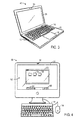
- FIG. 3 is a perspective view of the electronic device of FIG. 1 in the form of a laptop computing device, in accordance with aspects of the present disclosure
- FIG. 4 is a front view of the electronic device of FIG. 1 in the form of a desktop computing device, in accordance with aspects of the present disclosure
- FIG. 5 is a front view of the electronic device of FIG. 1 in the form of a handheld portable electronic device, in accordance with aspects of the present disclosure
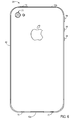
- FIG. 6 is a rear view of the electronic device shown in FIG. 5 ;
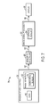
- FIG. 7 is a block diagram illustrating an embodiment of the image processing circuitry of FIG. l, in accordance with aspects of the present disclosure
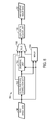
- FIG. 8 is a block diagram illustrating an embodiment of a horizontal scaler in an image sensor of FIG. 7 , in accordance with aspects of the present disclosure
- FIG. 9 is a flow diagram illustrating a method for transferring image data to an image signal processor, in accordance with aspects of the present disclosure.
- FIG. 10 is a flow diagram illustrating a method for correcting defective pixels in image data, in accordance with aspects of the present disclosure
- FIG. 11 is a diagram illustrating a pixel array that serves as an example for detecting defective pixels using the method described in FIG. 10 , in accordance with aspects of the present disclosure
- FIG. 12A is a diagram illustrating a phase error that occurs as a result of binning image data.
- FIG. 12B is a diagram illustrating horizontally demosaiced image data, in accordance with aspects of the present disclosure.
- the present disclosure relates generally to techniques for processing image data acquired via one or more image sensing devices.
- certain aspects of the present disclosure may relate to transferring image data to an image signal processor (ISP), detecting and correcting defective pixels in image data, and demosaicing image data.
- ISP image signal processor
- the presently disclosed techniques may be applied to both still images and moving images (e.g., video), and may be utilized in any suitable type of imaging application, such as a digital camera, an electronic device having an integrated digital camera, a security or video surveillance system, a medical imaging system, and so forth.
- FIG. 1 is a block diagram illustrating an example of an electronic device 10 that may provide for the processing of image data using one or more of the image processing techniques briefly mentioned above.
- the electronic device 10 may be any type of electronic device, such as a laptop or desktop computer, a mobile phone, a digital media player, or the like, that is configured to receive and process image data, such as data acquired using one or more image sensing components.
- the electronic device 10 may be a portable electronic device, such as a model of an iPod®, iPad®, or iPhone®, available from Apple Inc. of Cupertino, California.
- the electronic device 10 may be a desktop or laptop computer, such as a model of a MacBook®, MacBook® Pro, MacBook Air®, iMac®, Mac® Mini, or Mac Pro®, available from Apple Inc. In other embodiments, electronic device 10 may also be a model of an electronic device from another manufacturer that is capable of acquiring and processing image data.
- the electronic device 10 may provide for the processing of image data using one or more of the image processing techniques briefly mentioned above.
- the electronic device 10 may apply such image processing techniques to image data stored in a memory of the electronic device 10.
- the electronic device 10 may include one or more imaging devices, such as an integrated or external digital camera, configured to acquire image data, which may then be processed by the electronic device 10. Embodiments showing both portable and non-portable embodiments of electronic device 10 will be further discussed below in FIGS. 3-6 .
- the electronic device 10 may include various internal and/or external components, which contribute to the function of the device 10.
- the various functional blocks shown in FIG. 1 may comprise hardware elements (including circuitry), software elements (including computer code stored on a computer-readable medium) or a combination of both hardware and software elements.
- the electronic device 10 may include input/output (I/O) ports 12, input structures 14, one or more processors 16, memory device 18, non-volatile storage 20, networking device 24, power source 26, and display 28.
- the electronic device 10 may include one or more imaging devices 30, such as a digital camera, and an image signal processor (ISP) 32.
- image signal processor 32 may process image data that may be retrieved from the memory 18 and/or the non-volatile storage device(s) 20, or may be acquired using the imaging device 30.
- the system block diagram of the device 10 shown in FIG. 1 is intended to be a high-level control diagram depicting various components that may be included in such a device 10. That is, the connection lines between each individual component shown in FIG. 1 may not necessarily represent paths or directions through which data flows or is transmitted between various components of the device 10. Indeed, as discussed below, the depicted processor(s) 16 may, in some embodiments, include multiple processors, such as a main processor (e.g., CPU), and dedicated image and/or video processors.
- main processor e.g., CPU
- dedicated image and/or video processors dedicated image and/or video processors.
- the I/O ports 12 may include ports configured to connect to a variety of external devices, such as a power source, an audio output device (e.g., headset or headphones), or other electronic devices (such as handheld devices and/or computers, printers, projectors, external displays, modems, docking stations, and so forth).
- the I/O ports 12 may be configured to connect to an external imaging device, such as a digital camera, for the acquisition of image data that may be processed using the image signal processor 32.
- the I/O ports 12 may support any suitable interface type, such as a universal serial bus (USB) port, a serial connection port, an IEEE-1394 (FireWire) port, an Ethernet or modem port, and/or an AC/DC power connection port.
- USB universal serial bus
- IEEE-1394 FireWire
- the input structures 14 may provide user input or feedback to the processor(s) 16.
- input structures 14 may be configured to control one or more functions of electronic device 10, such as applications running on electronic device 10.
- input structures 14 may include buttons, sliders, switches, control pads, keys, knobs, scroll wheels, keyboards, mice, touchpads, and so forth, or some combination thereof.
- input structures 14 may allow a user to navigate a graphical user interface (GUI) displayed on device 10.
- GUI graphical user interface
- input structures 14 may include a touch sensitive mechanism provided in conjunction with display 28. In such embodiments, a user may select or interact with displayed interface elements via the touch sensitive mechanism.
- the input structures 14 may include the various devices, circuitry, and pathways by which user input or feedback is provided to one or more processors 16. Such input structures 14 may be configured to control a function of the device 10, applications running on the device 10, and/or any interfaces or devices connected to or used by the electronic device 10. For example, the input structures 14 may allow a user to navigate a displayed user interface or application interface.
- an input structure 14 and the display device 28 may be provided together, such as in the case of a "touchscreen,” whereby a touch-sensitive mechanism is provided in conjunction with the display 28.
- a touch-sensitive mechanism is provided in conjunction with the display 28.
- the user may select or interact with displayed interface elements via the touch-sensitive mechanism.
- the displayed interface may provide interactive functionality, allowing a user to navigate the displayed interface by touching the display 28.
- the input structures 14 may include an audio input device.
- one or more audio captures devices such as one or more microphones, may be provided with the electronic device 10.
- the audio capture devices may be integrated with the electronic device 10 or may be an external device coupled to the electronic device 10, such as by way of the I/O ports 12.
- the electronic device 10 may both an audio input device and imaging device 30 to capture sound and image data (e.g., video data), and may include logic configured to provide for synchronization of the captured video and audio data.
- the processor(s) 16 may control the general operation of the device 10. For instance, the processor(s) 16 may provide the processing capability to execute an operating system, programs, user and application interfaces, and any other functions of the electronic device 10.
- the processor(s) 16 may include one or more microprocessors, such as one or more "general-purpose" microprocessors, one or more special-purpose microprocessors and/or application-specific microprocessors (ASICs), or a combination of such processing components.
- the processor(s) 16 may include one or more instruction set (e.g., RISC) processors, as well as graphics processors (GPU), video processors, audio processors and/or related chip sets.
- the processor(s) 16 may be coupled to one or more data buses for transferring data and instructions between various components of the device 10.
- the processor(s) 16 may provide the processing capability to execute an imaging applications on the electronic device 10, such as Photo Booth®, Aperture®, iPhoto®, or Preview®, available from Apple Inc., or the "Camera” and/or "Photo” applications provided by Apple Inc. and available on models of the iPhone® or iPad®.
- the instructions or data to be processed by the processor(s) 16 may be stored in a computer-readable medium, such as a memory device 18.
- the memory device 18 may be provided as a volatile memory, such as random access memory (RAM) or as a non-volatile memory, such as read-only memory (ROM), or as a combination of one or more RAM and ROM devices.
- the memory 18 may store a variety of information and may be used for various purposes.
- the memory 18 may store firmware for the electronic device 10, such as a basic input/output system (BIOS), an operating system, various programs, applications, or any other routines that may be executed on the electronic device 10, including user interface functions, processor functions, and so forth.
- the memory 18 may be used for buffering or caching during operation of the electronic device 10.
- the memory 18 include one or more frame buffers for buffering video data as it is being output to the display 28.
- the electronic device 10 may further include a non-volatile storage 20 for persistent storage of data and/or instructions.
- the non-volatile storage 20 may include flash memory, a hard drive, or any other optical, magnetic, and/or solid-state storage media, or some combination thereof.
- image data stored in the non-volatile storage 20 and/or the memory device 18 may be processed by the image signal processor 32 before being output on a display.
- the electronic device 10 also includes the network device 24, which may be a network controller or a network interface card (NIC) that may provide for network connectivity over a wireless 802.11 standard or any other suitable networking standard, such as a local area network (LAN), a wide area network (WAN), an Enhanced Data Rates for GSM Evolution (EDGE) network, a 3G data network, or the Internet.
- the network device 24 may be a Wi-Fi device, a radio frequency device, a Bluetooth® device, a cellular communication device, or the like.
- the power source 26 of the device 10 may include the capability to power the device 10 in both non-portable and portable settings.
- the device 10 may include one or more batteries, such as a Li-Ion battery, for powering the device 10.
- the battery may be re-charged by connecting the device 10 to an external power source, such as to an electrical wall outlet.
- the power source 26 may include a power supply unit (PSU) configured to draw power from an electrical wall outlet, and to distribute the power to various components of a non-portable electronic device, such as a desktop computing system.
- PSU power supply unit
- the display 28 may be used to display various images generated by device 10, such as a GUI for an operating system, or image data (including still images and video data) processed by the image signal processor 32, as will be discussed further below.
- the image data may include image data acquired using the imaging device 30 or image data retrieved from the memory 18 and/or non-volatile storage 20.
- the display 28 may be any suitable type of display, such as a liquid crystal display (LCD), plasma display, or an organic light emitting diode (OLED) display, for example.
- the display 28 may be provided in conjunction with the above-discussed touch-sensitive mechanism (e.g., a touch screen) that may function as part of a control interface for the electronic device 10.
- the illustrated imaging device(s) 30 may be provided as a digital camera configured to acquire both still images and moving images (e.g., video).
- the camera 30 may include a lens and one or more image sensors configured to capturing and converting light into electrical signals.
- the image sensor may include a CMOS image sensor (e.g., a CMOS active-pixel sensor (APS)) or a CCD (charge-coupled device) sensor.
- the image sensor in the camera 30 includes an integrated circuit having an array of pixels, wherein each pixel includes a photodetector for sensing light.
- the photodetectors in the imaging pixels generally detect the intensity of light captured via the camera lenses. However, photodetectors, by themselves, are generally unable to detect the wavelength of the captured light and, thus, are unable to determine color information.
- the image sensor may further include a color filter array (CFA) that may overlay or be disposed over the pixel array of the image sensor to capture color information.
- CFA color filter array
- the color filter array may include an array of small color filters, each of which may overlap a respective pixel of the image sensor and filter the captured light by wavelength.
- the color filter array and the photodetectors may provide both wavelength and intensity information with regard to light captured through the camera, which may be representative of a captured image.
- the color filter array may include a Bayer color filter array, which provides a filter pattern that is 50% green elements, 25% red elements, and 25% blue elements.
- FIG. 2 shows a 2x2 pixel block of a Bayer CFA includes two green elements (Gr and Gb), one red element (R), and one blue element (B).
- an image sensor that utilizes a Bayer color filter array may provide information regarding the intensity of the light received by the camera 30 at the green, red, and blue wavelengths, whereby each image pixel records only one of the three colors (RGB).
- This information which may be referred to as "raw image data” or data in the “raw domain,” may then be processed using one or more demosaicing techniques to convert the raw image data into a full color image, generally by interpolating a set of red, green, and blue values for each pixel.
- demosaicing techniques may be performed by the image signal processor 32.
- FIGS. 3-6 illustrate various forms that the electronic device 10 may take.
- the electronic device 10 may take the form of a computer, including computers that are generally portable (such as laptop, notebook, and tablet computers) as well as computers that are generally non-portable (such as desktop computers, workstations and/or servers), or other type of electronic device, such as handheld portable electronic devices (e.g., digital media player or mobile phone).
- FIGS. 3 and 4 depict the electronic device 10 in the form of a laptop computer 40 and a desktop computer 50, respectively.
- FIGS. 5 and 6 show front and rear views, respectively, of the electronic device 10 in the form of a handheld portable device 60.
- the depicted laptop computer 40 includes a housing 42, the display 28, the I/O ports 12, and the input structures 14.
- the input structures 14 may include a keyboard and a touchpad mouse that are integrated with the housing 42. Additionally, the input structure 14 may include various other buttons and/or switches which may be used to interact with the computer 40, such as to power on or start the computer, to operate a GUI or an application running on the computer 40, as well as adjust various other aspects relating to operation of the computer 40 (e.g., sound volume, display brightness, etc.).
- the computer 40 may also include various I/O ports 12 that provide for connectivity to additional devices, as discussed above, such as a FireWire® or USB port, a high definition multimedia interface (HDMI) port, or any other type of port that is suitable for connecting to an external device. Additionally, the computer 40 may include network connectivity (e.g., network device 26), memory (e.g., memory 20), and storage capabilities (e.g., storage device 22), as described above with respect to FIG. 1 .
- network connectivity e.g., network device 26
- memory e.g., memory 20
- storage capabilities e.g., storage device 22
- the laptop computer 40 may include an integrated imaging device 30 (e.g., camera).
- the laptop computer 40 may utilize an external camera (e.g., an external USB camera or a "webcam") connected to one or more of the I/O ports 12 instead of or in addition to the integrated camera 30.
- an external camera may be an iSight® camera available from Apple Inc.
- the camera 30, whether integrated or external, may provide for the capture and recording of images.
- Such images may then be viewed by a user using an image viewing application, or may be utilized by other applications, including video-conferencing applications, such as iChat®, and image editing/viewing applications, such as Photo Booth®, Aperture®, iPhoto®, or Preview®, which are available from Apple Inc.
- video-conferencing applications such as iChat®
- image editing/viewing applications such as Photo Booth®, Aperture®, iPhoto®, or Preview®, which are available from Apple Inc.
- the depicted laptop computer 40 may be a model of a MacBook®, MacBook® Pro, MacBook Air®, or PowerBook® available from Apple Inc.
- the computer 40 in one embodiment, may be a portable tablet computing device, such as a model of an iPad® tablet computer, also available from Apple Inc.
- FIG. 4 further illustrates an embodiment in which the electronic device 10 is provided as a desktop computer 50.
- the desktop computer 50 may include a number of features that may be generally similar to those provided by the laptop computer 40 shown in FIG. 4 , but may have a generally larger overall form factor.
- the desktop computer 50 may be housed in an enclosure 42 that includes the display 28, as well as various other components discussed above with regard to the block diagram shown in FIG. 1 .
- the desktop computer 50 may include an external keyboard and mouse (input structures 14) that may be coupled to the computer 50 via one or more I/O ports 12 (e.g., USB) or may communicate with the computer 50 wirelessly (e.g., RF, Bluetooth, etc.).
- the desktop computer 50 also includes an imaging device 30, which may be an integrated or external camera, as discussed above.
- the depicted desktop computer 50 may be a model of an iMac®, Mac® mini, or Mac Pro®, available from Apple Inc.
- the display 28 may be configured to generate various images that may be viewed by a user.
- the display 28 may display a graphical user interface ("GUI") 52 that allows the user to interact with an operating system and/or application running on the computer 50.
- GUI 52 may include various layers, windows, screens, templates, or other graphical elements that may be displayed in all, or a portion, of the display device 28.
- an operating system GUI 52 may include various graphical icons 54, each of which may correspond to various applications that may be opened or executed upon detecting a user selection (e.g., via keyboard/mouse or touchscreen input).
- the icons 54 may be displayed in a dock 56 or within one or more graphical window elements 58 displayed on the screen.
- the selection of an icon 54 may lead to a hierarchical navigation process, such that selection of an icon 54 leads to a screen or opens another graphical window that includes one or more additional icons or other GUI elements.
- the operating system GUI 52 displayed in FIG. 4 may be from a version of the Mac OS® operating system, available from Apple Inc.
- the electronic device 10 is further illustrated in the form of portable handheld electronic device 60, which may be a model of an iPod® or iPhone® available from Apple Inc.
- the handheld device 60 includes an enclosure 42, which may function to protect the interior components from physical damage and to shield them from electromagnetic interference.
- the enclosure 42 may be formed from any suitable material or combination of materials, such as plastic, metal, or a composite material, and may allow certain frequencies of electromagnetic radiation, such as wireless networking signals, to pass through to wireless communication circuitry (e.g., network device 24), which may be disposed within the enclosure 42, as shown in FIG. 5 .
- the enclosure 42 also includes various user input structures 14 through which a user may interface with the handheld device 60.
- each input structure 14 may be configured to control one or more respective device functions when pressed or actuated.
- one or more of the input structures 14 may be configured to invoke a "home" screen 42 or menu to be displayed, to toggle between a sleep, wake, or powered on/off mode, to silence a ringer for a cellular phone application, to increase or decrease a volume output, and so forth.
- the illustrated input structures 14 are merely exemplary, and that the handheld device 60 may include any number of suitable user input structures existing in various forms including buttons, switches, keys, knobs, scroll wheels, and so forth.
- the handheld device 60 may include various I/O ports 12.
- the depicted I/O ports 12 may include a proprietary connection port 12a for transmitting and receiving data files or for charging a power source 26 and an audio connection port 12b for connecting the device 60 to an audio output device (e.g., headphones or speakers).
- an audio output device e.g., headphones or speakers.
- the display device 28 may display various images generated by the handheld device 60.
- the display 28 may display various system indicators 64 providing feedback to a user with regard to one or more states of handheld device 60, such as power status, signal strength, external device connections, and so forth.
- the display may also display a GUI 52 that allows a user to interact with the device 60, as discussed above with reference to FIG. 4 .
- the GUI 52 may include graphical elements, such as the icons 54, which may correspond to various applications that may be opened or executed upon detecting a user selection of a respective icon 54.
- one of the icons 54 may represent a camera application 66 that may be used in conjunction with a camera 30 for acquiring images.
- FIG. 6 a rear view of the handheld electronic device 60 depicted in FIG. 5 is illustrated, which shows the camera 30 as being integrated with the housing 42 and positioned on the rear of the handheld device 60.
- image data acquired using the camera 30 may be processed using the image signal processor 32, which my include hardware (e.g., disposed within the enclosure 42) and/or software stored on one or more storage devices (e.g., memory 18 or non-volatile storage 20) of the device 60.
- Images acquired using the camera application 66 and the camera 30 may be stored on the device 60 (e.g., in storage device 20) and may be viewed at a later time using a photo viewing application 68.
- the handheld device 60 may also include various audio input and output elements.
- the audio input/output elements depicted generally by reference numeral 70, may include an input receiver, such as one or more microphones.
- the input receivers may be configured to receive user audio input, such as a user's voice.
- the audio input/output elements 70 may include one or more output transmitters.
- Such output transmitters may include one or more speakers, which may function to transmit audio signals to a user, such as during the playback of music data using a media player application 72.
- an additional audio output transmitter 74 may be provided, as shown in FIG. 5 .
- the output transmitter 74 may also include one or more speakers configured to transmit audio signals to a user, such as voice data received during a telephone call.
- the audio input/output elements 70 and 74 may operate in conjunction to function as the audio receiving and transmitting elements of a telephone.
- the imaging device 30 and the image signal processor 32 depicted in FIG. 1 will now focus on the imaging device 30 and the image signal processor 32 depicted in FIG. 1 .
- logic carried out by the imaging device 30 and the image signal processor 32 may be implemented using hardware and/or software components, some of which may include various processing units that define an image signal processing (ISP) pipeline.
- ISP image signal processing
- the following discussion may focus on aspects of the image processing techniques set forth in the present disclosure, particularly those relating to transferring image data from the imaging device 30 to the image signal processor 32.
- FIG. 7 a simplified top-level block diagram 78 depicting several functional components that may be implemented as part of the imaging device 30 and the image signal processor 32 are illustrated, in accordance with one embodiment of the presently disclosed techniques. Particularly, FIG. 7 is intended to illustrate how image data may be transferred from the imaging device 30 to the image signal processor 32, in accordance with at least one embodiment. In order to provide a general overview, a general description of how these functional components operate to transfer image data is provided here with reference to FIG. 7 , while a more specific description of the image sensor 82 will be further provided below.
- the imaging device 30 may include a camera having one or more lenses 80 and image sensor(s) 82.
- the image sensor(s) 82 may include a horizontal scaler 84 that may process raw image data acquired by the image sensor(s) 82.
- the image sensor(s) 82 may include a color filter array (e.g., a Bayer filter) and may thus provide both light intensity and wavelength information captured by each imaging pixel of the image sensors 82.
- the light intensity and wavelength information may be packaged together as raw image data, which may be sent to the image signal processor 32 for processing via a sensor-to-image signal processor (ISP) data link 86.
- ISP sensor-to-image signal processor
- the image signal processor 32 may send the processed image data to the display 28.
- the image signal processor 32 and the sensor-to-ISP data link 86 may have sufficient processing resources to process the raw image data such that the display 28 may receive and display the image(s) depicted in the image data.
- the image signal processor 32 and the sensor-to-ISP data link 86 may need to process the raw image data at a very high rate in order for the display 28 to display the image(s) depicted in the raw image data effectively.
- the image sensor 82 may reduce the resolution of the raw image data and send the lower resolution or modified image data to the image signal processor 32 via the sensor-to-ISP data link 86.
- the image sensor 82 may horizontally downscale the raw image data such that the sensor-to-ISP data link 86 and the image signal processor 32 may be capable of processing the raw image data at their standard rates.
- the image sensor 82 may use a horizontal scaler 84 to downscale or down-sample the raw image data horizontally and generate anamorphic image data 92.
- the horizontal scaler 84 may then send the anamorphic image data 92 to the image signal processor 32 for processing via the sensor-to-ISP data link 86. In this manner, the anamorphic image data 92 consumes half as much bandwidth on the sensor-to-ISP data link 86 as compared to the raw image data.
- the anamorphic image data 92 may include more image information or detail as compared to binned image data, which would have been scaled with respect to two directions (i.e., horizontal and vertical).
- the image signal processor 32 may process the anamorphic image data 92 by performing one or more image processing operations, such as temporal filtering and the like.
- the processed anamorphic image data may then be input into a vertical scaler 94, or may be sent to a memory.
- the vertical scaler 94 may vertically downscale or down-sample the processed anamorphic image data and generate final resolution image data 96 that may be displayed on the display 28.
- horizontally scaling the raw image data before sending the data to the image signal processor 32 is similar to binning the raw image data in that it attempts to reduce the image resolution of the raw image data before transmission.
- the horizontal and vertical scaling operations are divided between the image sensor 82 and the image signal processor 32, as opposed to being performed solely on the image sensor 82 (e.g., binning), the image sensor 82 and the image signal processor 32 may be used more efficiently to display a higher quality image(s) as compared to binning.
- the horizontal scaler 84 may use one or more resampling filters that have a large number of'taps' or delays. Taps used in resampling filters indicate locations within an array of pixels of the raw image data where respective pixel data may be stored for scaling operations.
- the resampling filters may generate the downscaled image data by using a filtering function that produces one output pixel based on a range of nearby input pixels.
- a high-quality filter may use many taps to store information on many input pixels (e.g., 12) and produce one output pixel.
- a low-quality filter may use a small number of taps to store information on a small number of input pixels and produce one output pixel.
- the resulting image from the low-quality filter may include aliasing artifacts or excessive blurring.
- each output pixel depends on a number of nearby input pixels, each individual input pixel is used as input to a filter for multiple output pixels. As such, image data for each individual input pixel may be retained, or stored, by the filter until all output pixels it depends on have been processed.
- a horizontal resampling filter does not require a large amount of internal storage to retain image data for a range of horizontally-adjacent pixels that may be used by the horizontal resampling filter. Instead, the horizontal resampling filter may latch image data for a small number of pixels in simple register storage elements.
- a vertical resampling filter may use vertically-adj acent pixels to produce an output pixel. Vertically-adjacent pixels are separated in time by an entire image scan line. As such, the vertical resampling filter may retain image data for an entire row of image pixels for each of the vertically-adjacent pixels to perform its filtering function.
- a vertical resampling filter may use a significant additional amount of memory as compared to a horizontal resampling filter.
- an efficient vertical resampling filter would use many taps (e.g., 12 or more) to resample the image data
- a relatively large amount of memory may be used to apply an efficient vertical resampling filter to the raw image data.
- the image sensor 82 may not have a sufficient amount of memory to employ an efficient vertical resampling filter.
- the image sensor 82 may include an on-sensor RAM array that may be sufficient to latch image data for a small number pixels in simple register storage elements (i.e., for horizontal resampling filter).
- the on-sensor RAM array may not be sufficient to employ an efficient vertical resampling filter because the silicon process that the image sensor 82 may use may not be conducive to having a large amount of memory (e.g., efficient large RAM arrays). Instead, the area on the image sensor 82 required a large amount of memory would be significant and would reduce the area available for implementing more sensor pixels.
- the image sensor 82 may perform horizontal scaling-but leave vertical scaling to the image signal processor 32. Namely, the image sensor 82 may use the horizontal scaler 84 to horizontally downscale the raw image data (i.e., anamorphic image data 92) before sending it to the sensor-to-ISP data link 86 and the image signal processor 32. Additional details with regard to the horizontal scaler 84 are provided below with reference to FIG. 8 and FIG. 9 .
- the image signal processor 32 may process the anamorphic image data 92 and forward the processed anamorphic image data to a vertical scaler 94.
- the vertical scaler 94 may apply the vertical resampling filter to the processed anamorphic image data to generate a final output image data 96, which may be displayed on the display 28.
- applying the vertical resampling filter may involve a relatively large amount of memory as compared to applying the horizontal resampling filter, the image signal processor 32 may already include a sufficient amount of memory to apply the vertical resampling filter with an adequate amount of vertical taps to generate a high quality image(s).
- the horizontal scaler 84 may identify and correct for defective pixels in the raw image data and may preprocess the raw image data to improve the image quality of horizontally downscaled image data (i.e., anamorphic image data 92).
- FIG. 8 illustrates a block diagram of components in the horizontal scaler 84 that may be used to perform these operations.
- the horizontal scaler 84 may receive raw image data 98 and process it using a defective pixel correction unit 100, a demosaic unit 102, a mixer 104, a multiplexer 106, and a horizontal scaler unit 108. As illustrated in FIG.
- the raw image data 98 may be processed by the defective pixel correction unit 100 and the demosaic unit 102 before being horizontally downscaled by the horizontal scaler unit 108.
- the horizontal scaler 84 may not include the defective pixel correction unit 100, the demosaic unit 102, or both.
- correcting for defective pixels in the raw image data or demosaicing the raw image data may be optional processing steps for the horizontal scaler 84. Additional details with regard to the processing steps performed by the horizontal scaler 84 including the defective pixel correction unit 100, the demosaic unit 102, the mixer 104, the multiplexer 106, and the horizontal scaler unit 108 are described below with reference to FIG. 9 .
- FIG. 9 illustrates a flow chart of a method 112 for transferring image data from the image sensor 82 to the image signal processor 32.
- the method 112 indicates a particular order of operation, it should be understood that the method 112 is not limited to the illustrated order. Instead, the method 112 may be performed in any suitable order. In one embodiment, the method 112 may be performed by the image sensor 82 and, in particular, by the horizontal scaler 84.
- the image sensor 82 may capture raw image data.
- the image sensor 82 may include a color filter array, which may provide both light intensity and wavelength information captured by each imaging pixel of the image sensor 82.
- the raw image data may include a set of data that includes both light intensity and wavelength information for each imaging pixel of the image sensor 82.
- the raw image data may correspond to Bayer color filter array data.
- each scan line (i.e., row of pixels) in the raw image data may include either green and red pixel values or green and blue pixel values.
- the horizontal scaler 84 may use the horizontal scaler unit 108 to horizontally downscale the raw image data.
- the horizontal scaler unit 108 may perform the horizontal downscaling operation in a raw Bayer domain. As such, the horizontal scaler unit 108 may horizontally downscale the raw image data using pixel values of both colors in each scan line of the raw image data.
- the horizontal scaler unit 108 may horizontally downscale the raw image data using a horizontal resampling filter, such as a multi-tap polyphase filter.
- the multi-tap polyphase filter may multiply each pixel value in the raw image data by a weighting (or coefficient) factor (could be negative).
- the multi-tap polyphase filter may then sum the weighted horizontally adjacent pixels together to form a pixel value for a respective pixel.
- the pixels that correspond to the weighted horizontally adjacent pixels may depend on the position of the respective pixel and the number of taps used in the horizontal resampling filter.
- the weighting factors may be stored in a table and may be determined based on a current between-pixel fractional position.
- the weighting factors may be determined using one of a number well-known filter design techniques to produce a low-pass (i.e., antialiasing) digital filter.
- the low-pass digital filter may be a finite-impulse response filter such that its coefficients may be generated by applying a windowing function to an ideal low-pass filter function (e.g., a sinc function).
- the low-pass filter may remove high-frequency components that may produce aliases in output images from the image data.
- the horizontal resampling filter may be a horizontal low-pass filter on both color streams of a respective row of pixels in the raw image data.
- the horizontal low-pass filter may be a 1 ⁇ 2 pass zero-phase filter suitable for performing a 2:1 downscale of the raw image data.
- the 1 ⁇ 2 pass filter may preserve high-frequency information between the two color streams of the respective row of pixels in the raw image data, which may then be recovered by the image signal processor 32.
- the horizontal scaler unit 108 may use a Digital Differential Analyzer (DDA) to control the current position of a respective pixel during the scaling operation all of the raw image data.
- DDA Digital Differential Analyzer
- the horizontal scaling operation performed by the horizontal scaler unit 108 may include: (1) initializing the DDA; (2) performing a multi-tap polyphase filtering of the raw image data using an integer and fractional portions of the DDA; (3) adding a step value to the DDA; and repeating elements (2) and (3) for each pixel in the raw image data.
- the multi-tap polyphase filtering process of element (2) may include acquiring source pixel values of the pixels surrounding a respective pixel and multiplying the source pixel values by the appropriate weights or coefficients.
- the horizontal resampling filter may have 15 taps.
- the 15-tap filter may horizontally downscale the raw image data using a center pixel value (i.e., respective pixel) and seven additional pixel values on either side of the center pixel (e.g., -7, -6, -5, -4, -3, -2, -1, 0, +1, +2, +3, +4, +5, +6, +7).
- the horizontal scaler unit 108 may output pixels in the same Bayer order as the input pixels as the anamorphic image data 92.
- the horizontal scaler unit 108 may send the anamorphic image data 92 to the image signal processor 32 via the sensor-to-ISP data link 86.
- the horizontal scaler 84 may identify and correct for defective pixels in the raw image data as will be described below with respect to block 120 in the method 112. It should be noted, however, that the horizontal scaler 84 may not necessarily correct for defective pixels in the raw image data as described with respect to block 120. In other words, the raw image data could instead be horizontally downscaled without correcting the defective pixels.
- the image sensor 82 may use the defective pixel correction unit 100 in the horizontal scaler 84 to apply one-dimensional defective pixel correction to the raw image data at block 120.
- the one-dimensional defective pixel correction may identify defective pixels in the raw image data based on pixels located in the same scan line as a respective pixel.
- the defective pixel correction unit 100 may employ method 130, illustrated as a flow chart in FIG. 10 , to detect and correct defective pixels in the raw image data.
- the defective pixel correction unit 100 may receive a pixel value for a respective pixel in the raw image data at block 132.
- the defective pixel correction unit 100 may determine whether a difference between the received pixel value and each of its horizontally adjacent neighboring pixel values is greater than a threshold value. If the difference is not greater than the threshold value, the defective pixel correction unit 100 may move to the next pixel in the raw image data (decision block 136) and receive the next pixel value (block 132). If, however, the difference is greater than the threshold value (decision block 136), the defective pixel correction unit 100 may flag the respective pixel as a possible defective pixel (block 138).
- the defective pixel correction unit 100 may then save the location of the flagged pixel in a buffer (e.g., one bit per pixel). For pixels at the edge of the raw image data, the defective pixel correction unit 100 may extend the image by at least four pixels by replicating two edge pixels.
- the threshold value may be selected to maximize a number of correctly-detected defective pixels while minimizing the number of incorrectly detected pixels using a statistical analysis of sample images.
- the threshold may not be constant. Instead, it may vary based the scene content (e.g., exposure, etc.) of the image data.
- the defective pixel correction unit 100 may determine whether the flagged pixel's immediate horizontally, vertically, or diagonally adjacent neighboring pixels were previously flagged as possible defective pixels. Since the image sensor 82 outputs the raw image data in a horizontal line-by-line basis, the defective pixel correction unit 100 may only have data regarding whether five immediate neighboring pixels located one pixel away (i.e., to the left, right, up-left, above, and up-right of the respective pixel) have been flagged in the manner of block 138. For pixels on the first row of the raw image data, the defective pixel correction unit 100 may assume that the first row of pixels has a virtual row of pixels located above it such that none of the previous row's pixels has been flagged. If the defective pixel correction unit 100 determines that any of the five immediate neighboring pixels have been flagged, then the defective pixel correction unit 100 may move to the next pixel in the raw image data (block 136).
- the defective pixel correction unit 100 may designate the respective flagged pixel as defective.
- the defective pixel correction unit 100 may then correct the defective pixel.
- the defective pixel correction unit 100 may replace the defective pixel using a linear filter and the pixel values of the pixels neighboring the defective pixel as shown below in Equation 1.
- Pc i ⁇ j ( P ⁇ i , j - 3 * DPCF comp ⁇ 0 + P ⁇ i , j - 1 * DPCF comp ⁇ 1 + P ⁇ i , j + 1 * DPCF comp ⁇ 2 + P ⁇ i , j + 3 * DPCF comp ⁇ 3 ( ( DPCF comp ⁇ 3 + P ⁇ i , j + 2 ) ⁇ ⁇ 11 + 2 ⁇ ⁇ 11 ) > > 12
- Equation 1 comp refers to the Bayer component (Gr/R/B/Gb) of pixel (i,j) and functions DPCF[4][4] refer to defective pixel correction filter coefficients.
- the defective pixel correction filter coefficients may be signed 16-bit numbers with 12 fractional bits, and each color component may have its own set of filter coefficients. Since the raw image data may be arranged according to a Bayer color filter array, P(i,j-2) and P(i,j+2) are same color of P(i,j).
- the defective pixel correction unit 100 may send the corrected raw image data to the horizontal scaler unit 108 via the multiplexer 106.
- the horizontal scaler 84 may send the original pixel value for the defective pixel from the raw image data 92 and the replacement pixel value, as determined by the defective pixel correction unit 100, to the mixer 104.
- the mixer 104 may mix the various image data according to any suitable weighting before forwarding the mixed image data to the horizontal scaler unit 108 via the multiplexer 106, as shown in FIG. 8 .
- the defective pixel correction unit 100 may occasionally overcorrect by identifying a defective pixel where none exists.
- Mixing the raw image data 98 with image data output by the defective pixel correction unit 100 may allow some of the image information lost when such defective pixel overcorrection occurs to be added back into the image data. Although actual defective pixel data in the raw image data 98 will reduce the image quality, the resulting data output by the mixer 104 may be less problematic than had the defective pixel correction had not occurred at all.
- FIG. 11 provides an example of a pixel array 150 representing raw image data 98 that may be analyzed using method 130.
- the defective pixel correction unit 100 may initially receive a pixel value for pixel 152A, which corresponds to the first pixel output by the image sensor 82. Since the pixel 152A is substantially similar to its neighboring pixel 152B, the difference between the pixel value for pixel 152A and pixel 152B will likely be zero, which will likely be less than the threshold value of block 134. As such, the defective pixel correction unit 100 may move to pixel 152B (block 136) and determine whether the difference between the pixel value of pixel 152B and those of its neighboring pixels is greater than the threshold value (block 134).
- the defective pixel correction unit 100 may determine that the difference between the pixel value for pixel 154B and pixel 154C may be greater than the threshold value because pixel 154B (white pixel) has a significantly different pixel value as compared to pixel 154C (black pixel). However, the difference between the pixel value for pixel 154C and its next neighboring pixel (pixel 154D) will likely be zero because both pixels are black. As such, the difference between the pixel value for pixel 154C and pixel 154D will likely be less than the threshold value. Since the difference between the pixel value for pixel 154C and both of its neighboring pixels are less than the threshold value, the defective pixel correction unit 100 may move to next pixel (block 136).
- Pixel 154H represents a defective pixel.
- the defective pixel correction unit 100 may identify pixel 154H as a defective pixel by first determining that the difference between the pixel value for pixel 154H and pixel 154G is greater than the threshold value because pixel 154H (black pixel) has a significantly different pixel value as compared to pixel 154G (white pixel). Similarly, the defective pixel correction unit 100 may determine that the difference between the pixel value for pixel 154H and pixel 1541 may be greater than the threshold value because pixel 154H (black pixel) has a significantly different pixel value as compared to pixel 1541 (white pixel).
- the defective pixel correction unit 100 may flag pixel 154H as a possible defective pixel (block 138). The defective pixel correction 100 may then store the location of flagged pixel in a buffer for future reference.
- the defective pixel correction unit 100 may determine that pixel 154H is indeed a defective pixel based on whether it is immediately adjacent to any other flagged pixels (block 140). As mentioned above, since the image sensor 82 outputs the raw image data as horizontal rows of pixels, the defective pixel correction unit 100 may only have information related to flagged pixels located one pixel away to the left, right, up-left, above, and up-right of the pixel 154H. As such, the defective pixel correction unit 100 may determine whether pixels 152G, 152H, 1521, 152G, and 154I were previously flagged according to its buffer. As shown in FIG. 11 , since none of the pixels immediately adjacent to the pixel 154H were previously flagged, the defective pixel correction unit 100 may designate the pixel 154H as a defective pixel.
- the defective pixel correction unit 100 may correct the pixel 154H by determining a replacement pixel value for the pixel 154H by linearly filtering the neighboring pixels of pixel 154H.
- pixel 156H is not a defective pixel. Indeed, pixel 156H may represent a first pixel in a line of vertical pixels of similar color. Such an image may be obtained when the imaging device 30 captures an image of text on paper, which may have stark black letters against a white background.
- the defective pixel correction unit 100 may identify pixel 156H as a defective pixel, however, because the difference between its pixel value (i.e., black pixel) and each of its horizontally-neighboring pixels (i.e., white pixels) are greater than the threshold value and none of the pixels immediately adjacent (in the previous or same row) to 156H has been flagged as possible defective pixels. Although the defective pixel correction unit 100 may incorrectly identify pixel 156H as a defective pixel, this erroroneous designation will be limited to just one pixel in a vertical line of similar distinct pixels.
- the defective pixel correction unit 100 when the defective pixel correction unit 100 evaluates pixel 158H using method 130, the defective pixel correction unit 100 will flag pixel 158H as a possible defective pixel (block 134), but it will not designate pixel 158H as a defective pixel because the pixel immediately above it (pixel 156G) was previously flagged (block 140). Similarly, the defective pixel correction unit 100 will not identify the other pixels directly underneath pixel 156H and pixel 158H as defective pixels because each of those pixels will be flagged as possibly being defective like pixel 156H and pixel 158H. As such, since the pixel immediately above the respective pixel is flagged, as discussed above with reference to block 140 of FIG. 10 , the respective pixel will not be identified as a defective pixel.
- the image sensor 82 may not be able to employ a two-dimensional defective pixel correction process, which may be more effective than the one-dimensional defective pixel correction process employed in method 130. However, by performing some defective pixel correction process on the raw image data, the image sensor 82 may send higher quality image data to the image signal processor 32, which may yield higher quality images on the display 28.
- the image sensor 182 may perform a one-dimensional demosaic operation on the raw image data (block 122) using the demosaic unit 102 shown in FIG. 8 .
- the image signal processor 32 may be capable of performing demosaicing operations that may be more effective than the one-dimensional demosaic operation, by demosaicing the raw image data before horizontal downscaling, the demosaic unit 102 may enable the horizontal scaler unit 108 to retain more horizontal detail in the anamorphic image data 92 sent to the image signal processor 32.
- the resulting image(s) displayed on the display 28 may be significantly improved as compared to a binned version of the raw image data displayed on the display 28. It should be noted, however, that alternative embodiments may not involve demosaicing the raw image data as described with respect to block 122, and the raw image data could instead be horizontally downscaled without being demosaiced.
- a row 170 of raw image data may include red pixels 172 and green pixels 174.
- the binned image data of the row 170 may be generated based on pixel values of similarly colored adjacent pixels. For instance, since row 170 includes red pixels interleaved with green pixels, each binned red pixel (e.g., pixel 176A and pixel 176B) may be determined based on the pixel value of adjacent red pixels (e.g., pixel 172A and pixel 172B or pixel 172C and pixel 172D).
- the binned image data may include red pixel 176A that may be determined based on red pixels 172A and 172B.
- the binned image data may include a green pixel 178A that may be determined based on green pixels 174A and 174B.
- the resulting binned image data includes a sampling phase error due to the manner in which the raw image data was binned. In addition to the phase error, the resulting binned image data also loses image detail, since there is no cross-correlation between the different color channels. That is, although the raw image data may have high-frequency detail in terms of its pixel resolution, much of this resolution is lost in binning because the binning process averages pixel values from relatively distant pixels of the same color.
- the demosaic unit 102 may apply a one-dimensional horizontal demosaic algorithm on each scan line of the raw image data such that the resulting image data retains more horizontal detail as compared to a binned version of the raw image data.
- the demosaic unit 102 may receive a stream of Bayer pixels from the raw image data and output a stream of 2-color pixel values.
- Each of the 2-color pixel values may include the original pixel value and an interpolated value for a different color component on the row.
- FIG. 12B illustrates a row 170 of the raw image data that includes red pixels interleaved with green pixels.
- the demosaic unit 102 may interpolate each pixel value using both red and green pixels. That is, the demosaic unit 102 may generate pixel 180A such that it includes the original red pixel value for pixel 172A and an interpolated value for green (i.e., G').
- the interpolation of the respective pixel's adjacent color may be performed using a horizontal linear filter.
- the horizontal linear filter may cross correlate the pixels that are horizontally adjacent (i.e., pixels of both colors) to the respective pixel to determine the interpolated value for the respective pixel's other color component.
- the demosaic unit 102 may extend the image with four pixels by replicating two edge pixels.
- the demosaic unit 102 has been described as interpolating a pixel's color using linear interpolation methods, it should be noted that in some embodiments the interpolation of the pixel's color may be performed by non-linear interpolation methods (i.e., edge-sensitive methods).
- Each pixel in the resulting demosaiced image data 184 may include the original pixel value for the original pixel color and an interpolated pixel value for the respective pixel's adjacent color.
- the demosaic unit 108 may then send the demosaiced image data 184 to the multiplexer 106, which may forward the demosaiced image data 184to the horizontal scaler unit 108.
- the resulting anamorphic image data 92 may be sent to the image signal processor 32 via the sensor-to-ISP data link 86.
- the image signal processor 32 may process the anamorphic image data 92 and/or send the resulting image data to the vertical scaler 94, which may vertically downscale the image data to generate final resolution image data 96.
- the final resolution image data 96 may include additional horizontal detail with regard to the original raw image as compared to a binned version of the raw image data. As such, the final resolution image data 96 may produce significantly higher quality images on the display 28 as compared to the binned version of the raw image data.
- the multiplexer may also receive an input from the mixer 104, which may include information related to the original raw image data and the corrected defective pixels.
- the method 112 may also be performed by correcting for defective pixels in the raw image data and by demosaicing the raw image data as described in block 120 and block 122.
- horizontally demosaicing the image data may comprise applying a one-dimensional horizontal demosaic algorithm to one or more scan lines of the image data.
- horizontally downscaling the processed image data may comprise passing the processed image data through a low-pass filter on two color streams of each row of pixels in the processed image data.
- the low-pass filter may be a zero-phase half pass filter configured to perform a 2:1 downscale of the processed image data.
- the low pass filter may be configure to preserve high-frequency information between the two color streams of each row of pixels in the processed image data.
- the horizontally resampling filter may be a multi-tap polyphase filter.
- the multi-tap polyphase filter may have 15 taps.
- vertically downscaling the horizontally downscaled image data may comprise applying a vertical resampling filter with a plurality of vertical taps to the horizontally downscaled image.
- an electronic device comprising: a display configured to display one or more images; an image signal processor configured to send the one or more images to the display; and an image sensor configured to: receive image data; correct one or more defective pixels in the image data; horizontally downscale the defective pixel corrected image data; and send the horizontally downscaled image data to the image signal processor, wherein the image signal processor is configured to: receive the horizontally downscaled image data; vertically downscale the horizontally downscaled image data, thereby generating the one or more images; and sending the one or more images to the display device.
- the image sensor may store one or more locations of the defective pixels in a line buffer.
- an imaging device comprising: an image sensor configured to: process image data by: correcting one or more defective pixels in the image data; horizontally demosaicing the image data; or a combination thereof; horizontally downscale the processed image data; and send the horizontally downscaled image data to an image signal processor.
- a method comprising: receiving image data acquired by an image sensor; processing the image data by: correcting one or more defective pixels in the image data based on a one-dimensional defective pixel correction algorithm; horizontally demosaicing the image data based on a one-dimensional horizontal demosaic algorithm; or a combination thereof; horizontally downscaling the processed image data; processing the horizontally downscaled image data; and vertically downscaling the processed horizontally downscaled image.
Landscapes
- Engineering & Computer Science (AREA)
- Multimedia (AREA)
- Signal Processing (AREA)
- Physics & Mathematics (AREA)
- General Physics & Mathematics (AREA)
- Theoretical Computer Science (AREA)
- Studio Devices (AREA)
- Transforming Light Signals Into Electric Signals (AREA)
Abstract
Description
- The present disclosure relates generally to image processing and, more particularly, to systems and methods for initial image processing in an image sensor before additional processing in an image signal processor.
- This section is intended to introduce the reader to various aspects of art that may be related to various aspects of the present disclosure, which are described and/or claimed below. This discussion is believed to be helpful in providing the reader with background information to facilitate a better understanding of the various aspects of the present disclosure. Accordingly, it should be understood that these statements are to be read in this light, and not as admissions of prior art.
- Digital imaging devices have become increasing popular due, at least in part, to such devices becoming more and more affordable for the average consumer. Further, in addition to a number of stand-alone digital cameras currently available on the market, it is not uncommon for digital imaging devices to be integrated as part of another electronic device, such as a desktop or notebook computer, a cellular phone, or a portable media player.
- To acquire image data, most digital imaging devices include an image sensor that provides a number of light-detecting elements (e.g., photodetectors) configured to convert light detected by the image sensor into an electrical signal. An image sensor may also include a color filter array that filters light captured by the image sensor to capture color information. The image data captured by the image sensor may then be sent to an image processing pipeline (e.g., image signal processor (ISP)), which may apply a number of various image processing operations to the image data and generate a full color image that may be displayed for viewing on a display device, such as a monitor. In general, the image sensor may send the image data to the ISP via a sensor-to-ISP data link. As such, for still image data, the image sensor captures an image and sends the image as raw image data to the ISP via the sensor-to-ISP data link. The ISP and the sensor-to-ISP data link may generally be able process the raw image data at a standard rate such that it will effectively display the high-resolution image on a display device.
- Video image data, on the other hand, include a great deal more amount of data as compared to still image data. For instance, video images may include images captured at 30 to 60 frames per second (i.e., raw video data). Certain professional camera devices may process high-resolution raw video data in the ISP before downscaling the video data to a typical output resolution (e.g., 1920 x 1080). Processing each frame of the raw video data through the ISP, however, consumes significant processing and power resources. To avoid, many consumer camera devices may reduce the effective resolution of raw video data in the sensor before transferring the raw image data to the ISP.
- A common way to reduce the effective resolution of the raw video data is by "binning" the raw video data. Binning may include averaging adjacent groups of same-color pixels in each frame of the raw image data to make an effective lower-resolution sensor. For example, on a 4000x3000 pixel sensor, the sensor may be programmed to bin each 2x2 group of pixels and reduce the effective resolution of the pixel sensor to 2000x1500, which the ISP might crop and/or scale to a resolution of 1920x1080. Although the ISP and the sensor-to-ISP data link may more efficiently process the high-resolution images and video images received by the image sensor using the binning process, the quality of resulting video images may be unsatisfactory.
- A summary of certain embodiments disclosed herein is set forth below. It should be understood that these aspects are presented merely to provide the reader with a brief summary of these certain embodiments and that these aspects are not intended to limit the scope of this disclosure. Indeed, this disclosure may encompass a variety of aspects that may not be set forth below.
- The present disclosure relates generally to systems and method for transferring image data within an image processing system. In order to display high-resolution images and video images effectively, an image sensor may reduce the effective resolution of its raw image data. As used herein, the terms "raw video data" and "raw image data" both refer to image data captured by an image sensor during video capture. In this disclosure, these terms may be used substantially interchangeably. The sensor may send modified raw image data to an ISP via a sensor-to-ISP data link. The ISP and the sensor-to-ISP data link may process the modified image data to obtain a finished video viewable on a display device.
- Instead of simply binning the raw image data in the image sensor, which could result in a loss of image information, the image sensor may horizontally downscale the raw video image data to reduce the bandwidth of the raw image data by a factor of two. Horizontal downscaling may be a relatively resource-efficient operation to perform in the sensor. The image sensor may then send the horizontally downscaled image data to the ISP via the sensor-to-ISP data link. Once the ISP receives the downscaled image data, the ISP may vertically downscale it to generate a final output resolution of the image, which may be displayed on a display device.
- Additionally or alternatively, the image sensor may identify defective pixels from the raw image data before horizontally downscaling. In this manner, the image sensor may correct for defective pixels before downscaling the raw image data and before sending the downscaled image data to the ISP. Since defective pixels may be remedied before downscaling the video data, the defective pixels may have less impact on the quality of the ultimate video image data.
- The image sensor may employ one-dimensional defective pixel correction to determine whether a respective pixel is defective. This one-dimensional defective pixel correction may use fewer resources than defective pixel correction of the type usually found in an ISP. Reviewing pixel data as it is output, line by line, the image sensor may determine whether neighboring pixels of the same color component differ by more than a threshold value. Since the defective pixel correction is generally one-dimensional-relying mainly on pixel data from the current scan line and not at all on future scan lines-the image sensor may compare a pixel to its left and right adjacent neighbors. If the difference between neighboring pixels is greater than this threshold value, the image sensor may flag the respective pixel as possibly being defective. The image sensor may then designate the flagged pixel as a defective pixel if none of the flagged pixel's immediately neighboring pixels (i.e., one pixel away in lateral and above directions) are flagged. After designating a pixel as a defective pixel, the image sensor may replace the value of the defective pixel using a linear filter and the pixel values from the defective pixel's neighboring pixels.
- The image sensor may also, in some instances, perform a one-dimensional demosaic operation on the raw image data before horizontally downscaling the raw image. When demosaicing the raw image data, the image sensor may receive the raw image data as streams of pixels (i.e., rows of pixels) and output a stream of two-color pixel values such that each of the two-color pixel values may correspond to one of the pixels of the raw image data. The two-color pixel value may include an original pixel color value that corresponds to the color component of a respective pixel and an interpolated pixel color value that corresponds to a color component of the respective pixel's horizontally adjacent pixel. The stream of two-color pixel values created by the demosaicing operation may then be horizontally downscaled by the image sensor and sent to the ISP via the sensor-to-ISP data link. The demosaicing operation may enable the horizontally downscaled image data to retain some of the horizontal detail that may have been lost if the raw image data was horizontally downscaled without demosaicing.
- Various aspects of this disclosure may be better understood upon reading the following detailed description and upon reference to the drawings in which:
-
FIG. 1 is a simplified block diagram depicting components of an example of an electronic device that includes an imaging device and image processing circuitry configured to implement one or more of the image processing technique set forth in the present disclosure; -
FIG. 2 shows a graphical representation of a 2x2 pixel block of a Bayer color filter array that may be implemented in the imaging device ofFIG. 1 ; -
FIG. 3 is a perspective view of the electronic device ofFIG. 1 in the form of a laptop computing device, in accordance with aspects of the present disclosure; -
FIG. 4 is a front view of the electronic device ofFIG. 1 in the form of a desktop computing device, in accordance with aspects of the present disclosure; -
FIG. 5 is a front view of the electronic device ofFIG. 1 in the form of a handheld portable electronic device, in accordance with aspects of the present disclosure; -
FIG. 6 is a rear view of the electronic device shown inFIG. 5 ; -
FIG. 7 is a block diagram illustrating an embodiment of the image processing circuitry of FIG. l, in accordance with aspects of the present disclosure; -
FIG. 8 is a block diagram illustrating an embodiment of a horizontal scaler in an image sensor ofFIG. 7 , in accordance with aspects of the present disclosure; -
FIG. 9 is a flow diagram illustrating a method for transferring image data to an image signal processor, in accordance with aspects of the present disclosure; -
FIG. 10 is a flow diagram illustrating a method for correcting defective pixels in image data, in accordance with aspects of the present disclosure; -
FIG. 11 is a diagram illustrating a pixel array that serves as an example for detecting defective pixels using the method described inFIG. 10 , in accordance with aspects of the present disclosure; -
FIG. 12A is a diagram illustrating a phase error that occurs as a result of binning image data; and -
FIG. 12B is a diagram illustrating horizontally demosaiced image data, in accordance with aspects of the present disclosure; - One or more specific embodiments will be described below. In an effort to provide a concise description of these embodiments, not all features of an actual implementation are described in the specification. It should be appreciated that in the development of any such actual implementation, as in any engineering or design project, numerous implementation-specific decisions must be made to achieve the developers' specific goals, such as compliance with system-related and business-related constraints, which may vary from one implementation to another. Moreover, it should be appreciated that such a development effort might be complex and time consuming, but would nevertheless be a routine undertaking of design, fabrication, and manufacture for those of ordinary skill having the benefit of this disclosure.
- As will be discussed below, the present disclosure relates generally to techniques for processing image data acquired via one or more image sensing devices. In particular, certain aspects of the present disclosure may relate to transferring image data to an image signal processor (ISP), detecting and correcting defective pixels in image data, and demosaicing image data. It should be understood that the presently disclosed techniques may be applied to both still images and moving images (e.g., video), and may be utilized in any suitable type of imaging application, such as a digital camera, an electronic device having an integrated digital camera, a security or video surveillance system, a medical imaging system, and so forth.
- Keeping the above points in mind,
FIG. 1 is a block diagram illustrating an example of anelectronic device 10 that may provide for the processing of image data using one or more of the image processing techniques briefly mentioned above. Theelectronic device 10 may be any type of electronic device, such as a laptop or desktop computer, a mobile phone, a digital media player, or the like, that is configured to receive and process image data, such as data acquired using one or more image sensing components. By way of example, theelectronic device 10 may be a portable electronic device, such as a model of an iPod®, iPad®, or iPhone®, available from Apple Inc. of Cupertino, California. Additionally, theelectronic device 10 may be a desktop or laptop computer, such as a model of a MacBook®, MacBook® Pro, MacBook Air®, iMac®, Mac® Mini, or Mac Pro®, available from Apple Inc. In other embodiments,electronic device 10 may also be a model of an electronic device from another manufacturer that is capable of acquiring and processing image data. - Regardless of its form (e.g., portable or non-portable), it should be understood that the
electronic device 10 may provide for the processing of image data using one or more of the image processing techniques briefly mentioned above. In some embodiments, theelectronic device 10 may apply such image processing techniques to image data stored in a memory of theelectronic device 10. In further embodiments, theelectronic device 10 may include one or more imaging devices, such as an integrated or external digital camera, configured to acquire image data, which may then be processed by theelectronic device 10. Embodiments showing both portable and non-portable embodiments ofelectronic device 10 will be further discussed below inFIGS. 3-6 . - As shown in
FIG. 1 , theelectronic device 10 may include various internal and/or external components, which contribute to the function of thedevice 10. Those of ordinary skill in the art will appreciate that the various functional blocks shown inFIG. 1 may comprise hardware elements (including circuitry), software elements (including computer code stored on a computer-readable medium) or a combination of both hardware and software elements. For example, in the presently illustrated embodiment, theelectronic device 10 may include input/output (I/O)ports 12,input structures 14, one ormore processors 16,memory device 18,non-volatile storage 20,networking device 24,power source 26, anddisplay 28. Additionally, theelectronic device 10 may include one ormore imaging devices 30, such as a digital camera, and an image signal processor (ISP) 32. As can be appreciated,image signal processor 32 may process image data that may be retrieved from thememory 18 and/or the non-volatile storage device(s) 20, or may be acquired using theimaging device 30. - Before continuing, it should be understood that the system block diagram of the
device 10 shown inFIG. 1 is intended to be a high-level control diagram depicting various components that may be included in such adevice 10. That is, the connection lines between each individual component shown inFIG. 1 may not necessarily represent paths or directions through which data flows or is transmitted between various components of thedevice 10. Indeed, as discussed below, the depicted processor(s) 16 may, in some embodiments, include multiple processors, such as a main processor (e.g., CPU), and dedicated image and/or video processors. - With regard to each of the illustrated components in
FIG. 1 , the I/O ports 12 may include ports configured to connect to a variety of external devices, such as a power source, an audio output device (e.g., headset or headphones), or other electronic devices (such as handheld devices and/or computers, printers, projectors, external displays, modems, docking stations, and so forth). In one embodiment, the I/O ports 12 may be configured to connect to an external imaging device, such as a digital camera, for the acquisition of image data that may be processed using theimage signal processor 32. The I/O ports 12 may support any suitable interface type, such as a universal serial bus (USB) port, a serial connection port, an IEEE-1394 (FireWire) port, an Ethernet or modem port, and/or an AC/DC power connection port. - The
input structures 14 may provide user input or feedback to the processor(s) 16. For instance,input structures 14 may be configured to control one or more functions ofelectronic device 10, such as applications running onelectronic device 10. By way of example,input structures 14 may include buttons, sliders, switches, control pads, keys, knobs, scroll wheels, keyboards, mice, touchpads, and so forth, or some combination thereof. In one embodiment,input structures 14 may allow a user to navigate a graphical user interface (GUI) displayed ondevice 10. Additionally,input structures 14 may include a touch sensitive mechanism provided in conjunction withdisplay 28. In such embodiments, a user may select or interact with displayed interface elements via the touch sensitive mechanism. - The
input structures 14 may include the various devices, circuitry, and pathways by which user input or feedback is provided to one ormore processors 16.Such input structures 14 may be configured to control a function of thedevice 10, applications running on thedevice 10, and/or any interfaces or devices connected to or used by theelectronic device 10. For example, theinput structures 14 may allow a user to navigate a displayed user interface or application interface. - In certain embodiments, an
input structure 14 and thedisplay device 28 may be provided together, such as in the case of a "touchscreen," whereby a touch-sensitive mechanism is provided in conjunction with thedisplay 28. In such embodiments, the user may select or interact with displayed interface elements via the touch-sensitive mechanism. In this way, the displayed interface may provide interactive functionality, allowing a user to navigate the displayed interface by touching thedisplay 28. - In one embodiment, the
input structures 14 may include an audio input device. For instance, one or more audio captures devices, such as one or more microphones, may be provided with theelectronic device 10. The audio capture devices may be integrated with theelectronic device 10 or may be an external device coupled to theelectronic device 10, such as by way of the I/O ports 12. Theelectronic device 10 may both an audio input device andimaging device 30 to capture sound and image data (e.g., video data), and may include logic configured to provide for synchronization of the captured video and audio data. - In addition to processing various input signals received via the input structure(s) 14, the processor(s) 16 may control the general operation of the
device 10. For instance, the processor(s) 16 may provide the processing capability to execute an operating system, programs, user and application interfaces, and any other functions of theelectronic device 10. The processor(s) 16 may include one or more microprocessors, such as one or more "general-purpose" microprocessors, one or more special-purpose microprocessors and/or application-specific microprocessors (ASICs), or a combination of such processing components. For example, the processor(s) 16 may include one or more instruction set (e.g., RISC) processors, as well as graphics processors (GPU), video processors, audio processors and/or related chip sets. As will be appreciated, the processor(s) 16 may be coupled to one or more data buses for transferring data and instructions between various components of thedevice 10. In certain embodiments, the processor(s) 16 may provide the processing capability to execute an imaging applications on theelectronic device 10, such as Photo Booth®, Aperture®, iPhoto®, or Preview®, available from Apple Inc., or the "Camera" and/or "Photo" applications provided by Apple Inc. and available on models of the iPhone® or iPad®. - The instructions or data to be processed by the processor(s) 16 may be stored in a computer-readable medium, such as a
memory device 18. Thememory device 18 may be provided as a volatile memory, such as random access memory (RAM) or as a non-volatile memory, such as read-only memory (ROM), or as a combination of one or more RAM and ROM devices. Thememory 18 may store a variety of information and may be used for various purposes. For example, thememory 18 may store firmware for theelectronic device 10, such as a basic input/output system (BIOS), an operating system, various programs, applications, or any other routines that may be executed on theelectronic device 10, including user interface functions, processor functions, and so forth. In addition, thememory 18 may be used for buffering or caching during operation of theelectronic device 10. For instance, in one embodiment, thememory 18 include one or more frame buffers for buffering video data as it is being output to thedisplay 28. - In addition to the
memory device 18, theelectronic device 10 may further include anon-volatile storage 20 for persistent storage of data and/or instructions. Thenon-volatile storage 20 may include flash memory, a hard drive, or any other optical, magnetic, and/or solid-state storage media, or some combination thereof. In accordance with aspects of the present disclosure, image data stored in thenon-volatile storage 20 and/or thememory device 18 may be processed by theimage signal processor 32 before being output on a display. - The
electronic device 10 also includes thenetwork device 24, which may be a network controller or a network interface card (NIC) that may provide for network connectivity over a wireless 802.11 standard or any other suitable networking standard, such as a local area network (LAN), a wide area network (WAN), an Enhanced Data Rates for GSM Evolution (EDGE) network, a 3G data network, or the Internet. Thenetwork device 24 may be a Wi-Fi device, a radio frequency device, a Bluetooth® device, a cellular communication device, or the like. - The
power source 26 of thedevice 10 may include the capability to power thedevice 10 in both non-portable and portable settings. For example, in a portable setting, thedevice 10 may include one or more batteries, such as a Li-Ion battery, for powering thedevice 10. The battery may be re-charged by connecting thedevice 10 to an external power source, such as to an electrical wall outlet. In a non-portable setting, thepower source 26 may include a power supply unit (PSU) configured to draw power from an electrical wall outlet, and to distribute the power to various components of a non-portable electronic device, such as a desktop computing system. - The
display 28 may be used to display various images generated bydevice 10, such as a GUI for an operating system, or image data (including still images and video data) processed by theimage signal processor 32, as will be discussed further below. As mentioned above, the image data may include image data acquired using theimaging device 30 or image data retrieved from thememory 18 and/ornon-volatile storage 20. Thedisplay 28 may be any suitable type of display, such as a liquid crystal display (LCD), plasma display, or an organic light emitting diode (OLED) display, for example. Additionally, as discussed above, thedisplay 28 may be provided in conjunction with the above-discussed touch-sensitive mechanism (e.g., a touch screen) that may function as part of a control interface for theelectronic device 10. - The illustrated imaging device(s) 30 may be provided as a digital camera configured to acquire both still images and moving images (e.g., video). The
camera 30 may include a lens and one or more image sensors configured to capturing and converting light into electrical signals. By way of example, the image sensor may include a CMOS image sensor (e.g., a CMOS active-pixel sensor (APS)) or a CCD (charge-coupled device) sensor. Generally, the image sensor in thecamera 30 includes an integrated circuit having an array of pixels, wherein each pixel includes a photodetector for sensing light. As those skilled in the art will appreciate, the photodetectors in the imaging pixels generally detect the intensity of light captured via the camera lenses. However, photodetectors, by themselves, are generally unable to detect the wavelength of the captured light and, thus, are unable to determine color information. - Accordingly, the image sensor may further include a color filter array (CFA) that may overlay or be disposed over the pixel array of the image sensor to capture color information. The color filter array may include an array of small color filters, each of which may overlap a respective pixel of the image sensor and filter the captured light by wavelength. Thus, when used in conjunction, the color filter array and the photodetectors may provide both wavelength and intensity information with regard to light captured through the camera, which may be representative of a captured image.
- In one embodiment, the color filter array may include a Bayer color filter array, which provides a filter pattern that is 50% green elements, 25% red elements, and 25% blue elements. For instance,
FIG. 2 shows a 2x2 pixel block of a Bayer CFA includes two green elements (Gr and Gb), one red element (R), and one blue element (B). Thus, an image sensor that utilizes a Bayer color filter array may provide information regarding the intensity of the light received by thecamera 30 at the green, red, and blue wavelengths, whereby each image pixel records only one of the three colors (RGB). This information, which may be referred to as "raw image data" or data in the "raw domain," may then be processed using one or more demosaicing techniques to convert the raw image data into a full color image, generally by interpolating a set of red, green, and blue values for each pixel. Such demosaicing techniques may be performed by theimage signal processor 32. - Before continuing, it should be noted that while various embodiments of the various image processing techniques discussed below may utilize a Bayer CFA, the presently disclosed techniques are not intended to be limited in this regard. Indeed, those skilled in the art will appreciate that the image processing techniques provided herein may be applicable to any suitable type of color filter array, including RGBW filters, CYGM filters, and so forth.
- Referring again to the
electronic device 10,FIGS. 3-6 illustrate various forms that theelectronic device 10 may take. As mentioned above, theelectronic device 10 may take the form of a computer, including computers that are generally portable (such as laptop, notebook, and tablet computers) as well as computers that are generally non-portable (such as desktop computers, workstations and/or servers), or other type of electronic device, such as handheld portable electronic devices (e.g., digital media player or mobile phone). In particular,FIGS. 3 and 4 depict theelectronic device 10 in the form of alaptop computer 40 and adesktop computer 50, respectively.FIGS. 5 and6 show front and rear views, respectively, of theelectronic device 10 in the form of a handheldportable device 60. - As shown in
FIG. 3 , the depictedlaptop computer 40 includes ahousing 42, thedisplay 28, the I/O ports 12, and theinput structures 14. Theinput structures 14 may include a keyboard and a touchpad mouse that are integrated with thehousing 42. Additionally, theinput structure 14 may include various other buttons and/or switches which may be used to interact with thecomputer 40, such as to power on or start the computer, to operate a GUI or an application running on thecomputer 40, as well as adjust various other aspects relating to operation of the computer 40 (e.g., sound volume, display brightness, etc.). Thecomputer 40 may also include various I/O ports 12 that provide for connectivity to additional devices, as discussed above, such as a FireWire® or USB port, a high definition multimedia interface (HDMI) port, or any other type of port that is suitable for connecting to an external device. Additionally, thecomputer 40 may include network connectivity (e.g., network device 26), memory (e.g., memory 20), and storage capabilities (e.g., storage device 22), as described above with respect toFIG. 1 . - Further, the
laptop computer 40, in the illustrated embodiment, may include an integrated imaging device 30 (e.g., camera). In other embodiments, thelaptop computer 40 may utilize an external camera (e.g., an external USB camera or a "webcam") connected to one or more of the I/O ports 12 instead of or in addition to theintegrated camera 30. For instance, an external camera may be an iSight® camera available from Apple Inc. Thecamera 30, whether integrated or external, may provide for the capture and recording of images. Such images may then be viewed by a user using an image viewing application, or may be utilized by other applications, including video-conferencing applications, such as iChat®, and image editing/viewing applications, such as Photo Booth®, Aperture®, iPhoto®, or Preview®, which are available from Apple Inc. In certain embodiments, the depictedlaptop computer 40 may be a model of a MacBook®, MacBook® Pro, MacBook Air®, or PowerBook® available from Apple Inc. Additionally, thecomputer 40, in one embodiment, may be a portable tablet computing device, such as a model of an iPad® tablet computer, also available from Apple Inc. -
FIG. 4 further illustrates an embodiment in which theelectronic device 10 is provided as adesktop computer 50. As will be appreciated, thedesktop computer 50 may include a number of features that may be generally similar to those provided by thelaptop computer 40 shown inFIG. 4 , but may have a generally larger overall form factor. As shown, thedesktop computer 50 may be housed in anenclosure 42 that includes thedisplay 28, as well as various other components discussed above with regard to the block diagram shown inFIG. 1 . Further, thedesktop computer 50 may include an external keyboard and mouse (input structures 14) that may be coupled to thecomputer 50 via one or more I/O ports 12 (e.g., USB) or may communicate with thecomputer 50 wirelessly (e.g., RF, Bluetooth, etc.). Thedesktop computer 50 also includes animaging device 30, which may be an integrated or external camera, as discussed above. In certain embodiments, the depicteddesktop computer 50 may be a model of an iMac®, Mac® mini, or Mac Pro®, available from Apple Inc. - As further shown, the
display 28 may be configured to generate various images that may be viewed by a user. For example, during operation of thecomputer 50, thedisplay 28 may display a graphical user interface ("GUI") 52 that allows the user to interact with an operating system and/or application running on thecomputer 50. TheGUI 52 may include various layers, windows, screens, templates, or other graphical elements that may be displayed in all, or a portion, of thedisplay device 28. For instance, in the depicted embodiment, anoperating system GUI 52 may include variousgraphical icons 54, each of which may correspond to various applications that may be opened or executed upon detecting a user selection (e.g., via keyboard/mouse or touchscreen input). Theicons 54 may be displayed in adock 56 or within one or moregraphical window elements 58 displayed on the screen. In some embodiments, the selection of anicon 54 may lead to a hierarchical navigation process, such that selection of anicon 54 leads to a screen or opens another graphical window that includes one or more additional icons or other GUI elements. By way of example, theoperating system GUI 52 displayed inFIG. 4 may be from a version of the Mac OS® operating system, available from Apple Inc. - Continuing to
FIGS. 5 and6 , theelectronic device 10 is further illustrated in the form of portable handheldelectronic device 60, which may be a model of an iPod® or iPhone® available from Apple Inc. In the depicted embodiment, thehandheld device 60 includes anenclosure 42, which may function to protect the interior components from physical damage and to shield them from electromagnetic interference. Theenclosure 42 may be formed from any suitable material or combination of materials, such as plastic, metal, or a composite material, and may allow certain frequencies of electromagnetic radiation, such as wireless networking signals, to pass through to wireless communication circuitry (e.g., network device 24), which may be disposed within theenclosure 42, as shown inFIG. 5 . - The
enclosure 42 also includes varioususer input structures 14 through which a user may interface with thehandheld device 60. For instance, eachinput structure 14 may be configured to control one or more respective device functions when pressed or actuated. By way of example, one or more of theinput structures 14 may be configured to invoke a "home"screen 42 or menu to be displayed, to toggle between a sleep, wake, or powered on/off mode, to silence a ringer for a cellular phone application, to increase or decrease a volume output, and so forth. It should be understood that the illustratedinput structures 14 are merely exemplary, and that thehandheld device 60 may include any number of suitable user input structures existing in various forms including buttons, switches, keys, knobs, scroll wheels, and so forth. - As shown in
FIG. 5 , thehandheld device 60 may include various I/O ports 12. For instance, the depicted I/O ports 12 may include aproprietary connection port 12a for transmitting and receiving data files or for charging apower source 26 and anaudio connection port 12b for connecting thedevice 60 to an audio output device (e.g., headphones or speakers). - The
display device 28, which may be an LCD, OLED, or any suitable type of display, may display various images generated by thehandheld device 60. For example, thedisplay 28 may displayvarious system indicators 64 providing feedback to a user with regard to one or more states ofhandheld device 60, such as power status, signal strength, external device connections, and so forth. The display may also display aGUI 52 that allows a user to interact with thedevice 60, as discussed above with reference toFIG. 4 . TheGUI 52 may include graphical elements, such as theicons 54, which may correspond to various applications that may be opened or executed upon detecting a user selection of arespective icon 54. By way of example, one of theicons 54 may represent acamera application 66 that may be used in conjunction with acamera 30 for acquiring images. Referring briefly toFIG. 6 , a rear view of the handheldelectronic device 60 depicted inFIG. 5 is illustrated, which shows thecamera 30 as being integrated with thehousing 42 and positioned on the rear of thehandheld device 60. - As mentioned above, image data acquired using the
camera 30 may be processed using theimage signal processor 32, which my include hardware (e.g., disposed within the enclosure 42) and/or software stored on one or more storage devices (e.g.,memory 18 or non-volatile storage 20) of thedevice 60. Images acquired using thecamera application 66 and thecamera 30 may be stored on the device 60 (e.g., in storage device 20) and may be viewed at a later time using aphoto viewing application 68. - The
handheld device 60 may also include various audio input and output elements. For example, the audio input/output elements, depicted generally byreference numeral 70, may include an input receiver, such as one or more microphones. For instance, where thehandheld device 60 includes cell phone functionality, the input receivers may be configured to receive user audio input, such as a user's voice. Additionally, the audio input/output elements 70 may include one or more output transmitters. Such output transmitters may include one or more speakers, which may function to transmit audio signals to a user, such as during the playback of music data using amedia player application 72. Further, in embodiments where thehandheld device 60 includes a cell phone application, an additionalaudio output transmitter 74 may be provided, as shown inFIG. 5 . Like the output transmitters of the audio input/output elements 70, theoutput transmitter 74 may also include one or more speakers configured to transmit audio signals to a user, such as voice data received during a telephone call. Thus, the audio input/output elements - Having now provided some context with regard to various forms that the
electronic device 10 may take, the present discussion will now focus on theimaging device 30 and theimage signal processor 32 depicted inFIG. 1 . As mentioned above, logic carried out by theimaging device 30 and theimage signal processor 32 may be implemented using hardware and/or software components, some of which may include various processing units that define an image signal processing (ISP) pipeline. In particular, the following discussion may focus on aspects of the image processing techniques set forth in the present disclosure, particularly those relating to transferring image data from theimaging device 30 to theimage signal processor 32. - Referring now to
FIG. 7 , a simplified top-level block diagram 78 depicting several functional components that may be implemented as part of theimaging device 30 and theimage signal processor 32 are illustrated, in accordance with one embodiment of the presently disclosed techniques. Particularly,FIG. 7 is intended to illustrate how image data may be transferred from theimaging device 30 to theimage signal processor 32, in accordance with at least one embodiment. In order to provide a general overview, a general description of how these functional components operate to transfer image data is provided here with reference toFIG. 7 , while a more specific description of theimage sensor 82 will be further provided below. - Referring to the illustrated embodiment, the
imaging device 30 may include a camera having one ormore lenses 80 and image sensor(s) 82. In one embodiment, the image sensor(s) 82 may include ahorizontal scaler 84 that may process raw image data acquired by the image sensor(s) 82. As discussed above, the image sensor(s) 82 may include a color filter array (e.g., a Bayer filter) and may thus provide both light intensity and wavelength information captured by each imaging pixel of theimage sensors 82. The light intensity and wavelength information may be packaged together as raw image data, which may be sent to theimage signal processor 32 for processing via a sensor-to-image signal processor (ISP)data link 86. - After processing the raw image data, the
image signal processor 32 may send the processed image data to thedisplay 28. For smaller amounts of image data, theimage signal processor 32 and the sensor-to-ISP data link 86 may have sufficient processing resources to process the raw image data such that thedisplay 28 may receive and display the image(s) depicted in the image data. However, for larger amounts of image data (e.g., high-resolution images or video data), theimage signal processor 32 and the sensor-to-ISP data link 86 may need to process the raw image data at a very high rate in order for thedisplay 28 to display the image(s) depicted in the raw image data effectively. As discussed above, to process a large amount of raw image data, theimage sensor 82 may reduce the resolution of the raw image data and send the lower resolution or modified image data to theimage signal processor 32 via the sensor-to-ISP data link 86. - Instead of binning the raw image data, the
image sensor 82 may horizontally downscale the raw image data such that the sensor-to-ISP data link 86 and theimage signal processor 32 may be capable of processing the raw image data at their standard rates. In this case, theimage sensor 82 may use ahorizontal scaler 84 to downscale or down-sample the raw image data horizontally and generateanamorphic image data 92. Thehorizontal scaler 84 may then send theanamorphic image data 92 to theimage signal processor 32 for processing via the sensor-to-ISP data link 86. In this manner, theanamorphic image data 92 consumes half as much bandwidth on the sensor-to-ISP data link 86 as compared to the raw image data. - Since the
anamorphic image data 92 has been scaled in just one direction (i.e., horizontal), theanamorphic image data 92 may include more image information or detail as compared to binned image data, which would have been scaled with respect to two directions (i.e., horizontal and vertical). After receiving theanamorphic image data 92, theimage signal processor 32 may process theanamorphic image data 92 by performing one or more image processing operations, such as temporal filtering and the like. The processed anamorphic image data may then be input into avertical scaler 94, or may be sent to a memory. Thevertical scaler 94 may vertically downscale or down-sample the processed anamorphic image data and generate finalresolution image data 96 that may be displayed on thedisplay 28. - In some ways, horizontally scaling the raw image data before sending the data to the
image signal processor 32 is similar to binning the raw image data in that it attempts to reduce the image resolution of the raw image data before transmission. However, since the horizontal and vertical scaling operations are divided between theimage sensor 82 and theimage signal processor 32, as opposed to being performed solely on the image sensor 82 (e.g., binning), theimage sensor 82 and theimage signal processor 32 may be used more efficiently to display a higher quality image(s) as compared to binning. - Indeed, in order to produce a high-quality downscaled image data, the
horizontal scaler 84 may use one or more resampling filters that have a large number of'taps' or delays. Taps used in resampling filters indicate locations within an array of pixels of the raw image data where respective pixel data may be stored for scaling operations. The resampling filters may generate the downscaled image data by using a filtering function that produces one output pixel based on a range of nearby input pixels. In one embodiment, a high-quality filter may use many taps to store information on many input pixels (e.g., 12) and produce one output pixel. In contrast, a low-quality filter may use a small number of taps to store information on a small number of input pixels and produce one output pixel. The resulting image from the low-quality filter may include aliasing artifacts or excessive blurring. In any case, because each output pixel depends on a number of nearby input pixels, each individual input pixel is used as input to a filter for multiple output pixels. As such, image data for each individual input pixel may be retained, or stored, by the filter until all output pixels it depends on have been processed. - Since the
image sensor 82 scans out pixels horizontally, a horizontal resampling filter does not require a large amount of internal storage to retain image data for a range of horizontally-adjacent pixels that may be used by the horizontal resampling filter. Instead, the horizontal resampling filter may latch image data for a small number of pixels in simple register storage elements. A vertical resampling filter, however, may use vertically-adj acent pixels to produce an output pixel. Vertically-adjacent pixels are separated in time by an entire image scan line. As such, the vertical resampling filter may retain image data for an entire row of image pixels for each of the vertically-adjacent pixels to perform its filtering function. Thus, a vertical resampling filter may use a significant additional amount of memory as compared to a horizontal resampling filter. - Further, since an efficient vertical resampling filter would use many taps (e.g., 12 or more) to resample the image data, a relatively large amount of memory may be used to apply an efficient vertical resampling filter to the raw image data. The
image sensor 82, however, may not have a sufficient amount of memory to employ an efficient vertical resampling filter. For instance, theimage sensor 82 may include an on-sensor RAM array that may be sufficient to latch image data for a small number pixels in simple register storage elements (i.e., for horizontal resampling filter). However, the on-sensor RAM array may not be sufficient to employ an efficient vertical resampling filter because the silicon process that theimage sensor 82 may use may not be conducive to having a large amount of memory (e.g., efficient large RAM arrays). Instead, the area on theimage sensor 82 required a large amount of memory would be significant and would reduce the area available for implementing more sensor pixels. Thus, theimage sensor 82 may perform horizontal scaling-but leave vertical scaling to theimage signal processor 32. Namely, theimage sensor 82 may use thehorizontal scaler 84 to horizontally downscale the raw image data (i.e., anamorphic image data 92) before sending it to the sensor-to-ISP data link 86 and theimage signal processor 32. Additional details with regard to thehorizontal scaler 84 are provided below with reference toFIG. 8 andFIG. 9 . - After receiving the
anamorphic image data 92, theimage signal processor 32 may process theanamorphic image data 92 and forward the processed anamorphic image data to avertical scaler 94. Thevertical scaler 94 may apply the vertical resampling filter to the processed anamorphic image data to generate a finaloutput image data 96, which may be displayed on thedisplay 28. Although applying the vertical resampling filter may involve a relatively large amount of memory as compared to applying the horizontal resampling filter, theimage signal processor 32 may already include a sufficient amount of memory to apply the vertical resampling filter with an adequate amount of vertical taps to generate a high quality image(s). - In addition to horizontally downscaling the raw image data, the
horizontal scaler 84 may identify and correct for defective pixels in the raw image data and may preprocess the raw image data to improve the image quality of horizontally downscaled image data (i.e., anamorphic image data 92).FIG. 8 illustrates a block diagram of components in thehorizontal scaler 84 that may be used to perform these operations. For instance, in one embodiment, thehorizontal scaler 84 may receiveraw image data 98 and process it using a defectivepixel correction unit 100, ademosaic unit 102, amixer 104, amultiplexer 106, and ahorizontal scaler unit 108. As illustrated inFIG. 8 , theraw image data 98 may be processed by the defectivepixel correction unit 100 and thedemosaic unit 102 before being horizontally downscaled by thehorizontal scaler unit 108. However, it should be noted that in some embodiments, thehorizontal scaler 84 may not include the defectivepixel correction unit 100, thedemosaic unit 102, or both. As such, correcting for defective pixels in the raw image data or demosaicing the raw image data may be optional processing steps for thehorizontal scaler 84. Additional details with regard to the processing steps performed by thehorizontal scaler 84 including the defectivepixel correction unit 100, thedemosaic unit 102, themixer 104, themultiplexer 106, and thehorizontal scaler unit 108 are described below with reference toFIG. 9 . -
FIG. 9 illustrates a flow chart of amethod 112 for transferring image data from theimage sensor 82 to theimage signal processor 32. Although themethod 112 indicates a particular order of operation, it should be understood that themethod 112 is not limited to the illustrated order. Instead, themethod 112 may be performed in any suitable order. In one embodiment, themethod 112 may be performed by theimage sensor 82 and, in particular, by thehorizontal scaler 84. - At
block 114, theimage sensor 82 may capture raw image data. As mentioned above, theimage sensor 82 may include a color filter array, which may provide both light intensity and wavelength information captured by each imaging pixel of theimage sensor 82. As such, the raw image data may include a set of data that includes both light intensity and wavelength information for each imaging pixel of theimage sensor 82. In one embodiment, the raw image data may correspond to Bayer color filter array data. As such, each scan line (i.e., row of pixels) in the raw image data may include either green and red pixel values or green and blue pixel values. - At
block 116, thehorizontal scaler 84 may use thehorizontal scaler unit 108 to horizontally downscale the raw image data. Thehorizontal scaler unit 108 may perform the horizontal downscaling operation in a raw Bayer domain. As such, thehorizontal scaler unit 108 may horizontally downscale the raw image data using pixel values of both colors in each scan line of the raw image data. - In one embodiment, the
horizontal scaler unit 108 may horizontally downscale the raw image data using a horizontal resampling filter, such as a multi-tap polyphase filter. The multi-tap polyphase filter may multiply each pixel value in the raw image data by a weighting (or coefficient) factor (could be negative). The multi-tap polyphase filter may then sum the weighted horizontally adjacent pixels together to form a pixel value for a respective pixel. The pixels that correspond to the weighted horizontally adjacent pixels may depend on the position of the respective pixel and the number of taps used in the horizontal resampling filter. The weighting factors may be stored in a table and may be determined based on a current between-pixel fractional position. - The weighting factors may be determined using one of a number well-known filter design techniques to produce a low-pass (i.e., antialiasing) digital filter. In one embodiment, the low-pass digital filter may be a finite-impulse response filter such that its coefficients may be generated by applying a windowing function to an ideal low-pass filter function (e.g., a sinc function). The low-pass filter may remove high-frequency components that may produce aliases in output images from the image data.
- In another embodiment, the horizontal resampling filter may be a horizontal low-pass filter on both color streams of a respective row of pixels in the raw image data. The horizontal low-pass filter may be a ½ pass zero-phase filter suitable for performing a 2:1 downscale of the raw image data. The ½ pass filter may preserve high-frequency information between the two color streams of the respective row of pixels in the raw image data, which may then be recovered by the
image signal processor 32. - When horizontally downscaling the raw image, the
horizontal scaler unit 108 may use a Digital Differential Analyzer (DDA) to control the current position of a respective pixel during the scaling operation all of the raw image data. As such, the horizontal scaling operation performed by thehorizontal scaler unit 108 may include: (1) initializing the DDA; (2) performing a multi-tap polyphase filtering of the raw image data using an integer and fractional portions of the DDA; (3) adding a step value to the DDA; and repeating elements (2) and (3) for each pixel in the raw image data. - The multi-tap polyphase filtering process of element (2) may include acquiring source pixel values of the pixels surrounding a respective pixel and multiplying the source pixel values by the appropriate weights or coefficients. In one embodiment, the horizontal resampling filter may have 15 taps. Here, the 15-tap filter may horizontally downscale the raw image data using a center pixel value (i.e., respective pixel) and seven additional pixel values on either side of the center pixel (e.g., -7, -6, -5, -4, -3, -2, -1, 0, +1, +2, +3, +4, +5, +6, +7).
- After the raw image data is horizontally downscaled, the
horizontal scaler unit 108 may output pixels in the same Bayer order as the input pixels as theanamorphic image data 92. Atblock 118, thehorizontal scaler unit 108 may send theanamorphic image data 92 to theimage signal processor 32 via the sensor-to-ISP data link 86. - As discussed above, in addition to horizontally downscaling the raw image data, the
horizontal scaler 84 may identify and correct for defective pixels in the raw image data as will be described below with respect to block 120 in themethod 112. It should be noted, however, that thehorizontal scaler 84 may not necessarily correct for defective pixels in the raw image data as described with respect to block 120. In other words, the raw image data could instead be horizontally downscaled without correcting the defective pixels. - When the
horizontal scaler 84 performs defective pixel correction, theimage sensor 82 may use the defectivepixel correction unit 100 in thehorizontal scaler 84 to apply one-dimensional defective pixel correction to the raw image data atblock 120. The one-dimensional defective pixel correction may identify defective pixels in the raw image data based on pixels located in the same scan line as a respective pixel. In one embodiment, the defectivepixel correction unit 100 may employmethod 130, illustrated as a flow chart inFIG. 10 , to detect and correct defective pixels in the raw image data. - As seen in
FIG. 10 , the defectivepixel correction unit 100 may receive a pixel value for a respective pixel in the raw image data atblock 132. Atblock 134, the defectivepixel correction unit 100 may determine whether a difference between the received pixel value and each of its horizontally adjacent neighboring pixel values is greater than a threshold value. If the difference is not greater than the threshold value, the defectivepixel correction unit 100 may move to the next pixel in the raw image data (decision block 136) and receive the next pixel value (block 132). If, however, the difference is greater than the threshold value (decision block 136), the defectivepixel correction unit 100 may flag the respective pixel as a possible defective pixel (block 138). The defectivepixel correction unit 100 may then save the location of the flagged pixel in a buffer (e.g., one bit per pixel). For pixels at the edge of the raw image data, the defectivepixel correction unit 100 may extend the image by at least four pixels by replicating two edge pixels. - In one embodiment, the threshold value may be selected to maximize a number of correctly-detected defective pixels while minimizing the number of incorrectly detected pixels using a statistical analysis of sample images. In certain embodiments, the threshold may not be constant. Instead, it may vary based the scene content (e.g., exposure, etc.) of the image data.
- At
block 140, the defectivepixel correction unit 100 may determine whether the flagged pixel's immediate horizontally, vertically, or diagonally adjacent neighboring pixels were previously flagged as possible defective pixels. Since theimage sensor 82 outputs the raw image data in a horizontal line-by-line basis, the defectivepixel correction unit 100 may only have data regarding whether five immediate neighboring pixels located one pixel away (i.e., to the left, right, up-left, above, and up-right of the respective pixel) have been flagged in the manner ofblock 138. For pixels on the first row of the raw image data, the defectivepixel correction unit 100 may assume that the first row of pixels has a virtual row of pixels located above it such that none of the previous row's pixels has been flagged. If the defectivepixel correction unit 100 determines that any of the five immediate neighboring pixels have been flagged, then the defectivepixel correction unit 100 may move to the next pixel in the raw image data (block 136). - Alternatively, if the defective
pixel correction unit 100 determines that none of the five immediate neighboring pixels has been flagged, the defectivepixel correction unit 100 may designate the respective flagged pixel as defective. Atblock 142, the defectivepixel correction unit 100 may then correct the defective pixel. In one embodiment, the defectivepixel correction unit 100 may replace the defective pixel using a linear filter and the pixel values of the pixels neighboring the defective pixel as shown below in Equation 1.
- In Equation 1, comp refers to the Bayer component (Gr/R/B/Gb) of pixel (i,j) and functions DPCF[4][4] refer to defective pixel correction filter coefficients. The defective pixel correction filter coefficients may be signed 16-bit numbers with 12 fractional bits, and each color component may have its own set of filter coefficients. Since the raw image data may be arranged according to a Bayer color filter array, P(i,j-2) and P(i,j+2) are same color of P(i,j).
- Referring briefly again to
FIG. 8 , in one embodiment, after correcting for the defective pixel, the defectivepixel correction unit 100 may send the corrected raw image data to thehorizontal scaler unit 108 via themultiplexer 106. In another embodiment, thehorizontal scaler 84 may send the original pixel value for the defective pixel from theraw image data 92 and the replacement pixel value, as determined by the defectivepixel correction unit 100, to themixer 104. Themixer 104 may mix the various image data according to any suitable weighting before forwarding the mixed image data to thehorizontal scaler unit 108 via themultiplexer 106, as shown inFIG. 8 . As will be noted below, the defectivepixel correction unit 100 may occasionally overcorrect by identifying a defective pixel where none exists. Mixing theraw image data 98 with image data output by the defectivepixel correction unit 100 may allow some of the image information lost when such defective pixel overcorrection occurs to be added back into the image data. Although actual defective pixel data in theraw image data 98 will reduce the image quality, the resulting data output by themixer 104 may be less problematic than had the defective pixel correction had not occurred at all. - Keeping the
method 130 of one-dimensional defective pixel correction in mind,FIG. 11 provides an example of apixel array 150 representingraw image data 98 that may be analyzed usingmethod 130. Referring to block 132 ofmethod 130, the defectivepixel correction unit 100 may initially receive a pixel value forpixel 152A, which corresponds to the first pixel output by theimage sensor 82. Since thepixel 152A is substantially similar to itsneighboring pixel 152B, the difference between the pixel value forpixel 152A andpixel 152B will likely be zero, which will likely be less than the threshold value ofblock 134. As such, the defectivepixel correction unit 100 may move topixel 152B (block 136) and determine whether the difference between the pixel value ofpixel 152B and those of its neighboring pixels is greater than the threshold value (block 134). - When the defective
pixel correction unit 100 receives the pixel value forpixel 154C, the defectivepixel correction unit 100 may determine that the difference between the pixel value forpixel 154B andpixel 154C may be greater than the threshold value becausepixel 154B (white pixel) has a significantly different pixel value as compared topixel 154C (black pixel). However, the difference between the pixel value forpixel 154C and its next neighboring pixel (pixel 154D) will likely be zero because both pixels are black. As such, the difference between the pixel value forpixel 154C andpixel 154D will likely be less than the threshold value. Since the difference between the pixel value forpixel 154C and both of its neighboring pixels are less than the threshold value, the defectivepixel correction unit 100 may move to next pixel (block 136). -
Pixel 154H represents a defective pixel. The defectivepixel correction unit 100 may identifypixel 154H as a defective pixel by first determining that the difference between the pixel value forpixel 154H andpixel 154G is greater than the threshold value becausepixel 154H (black pixel) has a significantly different pixel value as compared topixel 154G (white pixel). Similarly, the defectivepixel correction unit 100 may determine that the difference between the pixel value forpixel 154H andpixel 1541 may be greater than the threshold value becausepixel 154H (black pixel) has a significantly different pixel value as compared to pixel 1541 (white pixel). Accordingly, since the difference between the pixel value forpixel 154H and each of its neighboring pixels are greater than the threshold value, the defectivepixel correction unit 100 may flagpixel 154H as a possible defective pixel (block 138). Thedefective pixel correction 100 may then store the location of flagged pixel in a buffer for future reference. - The defective
pixel correction unit 100 may determine thatpixel 154H is indeed a defective pixel based on whether it is immediately adjacent to any other flagged pixels (block 140). As mentioned above, since theimage sensor 82 outputs the raw image data as horizontal rows of pixels, the defectivepixel correction unit 100 may only have information related to flagged pixels located one pixel away to the left, right, up-left, above, and up-right of thepixel 154H. As such, the defectivepixel correction unit 100 may determine whetherpixels FIG. 11 , since none of the pixels immediately adjacent to thepixel 154H were previously flagged, the defectivepixel correction unit 100 may designate thepixel 154H as a defective pixel. - After identifying the defective pixel, the defective
pixel correction unit 100 may correct thepixel 154H by determining a replacement pixel value for thepixel 154H by linearly filtering the neighboring pixels ofpixel 154H.
Unlikepixel 154H,pixel 156H is not a defective pixel. Indeed,pixel 156H may represent a first pixel in a line of vertical pixels of similar color. Such an image may be obtained when theimaging device 30 captures an image of text on paper, which may have stark black letters against a white background. The defectivepixel correction unit 100 may identifypixel 156H as a defective pixel, however, because the difference between its pixel value (i.e., black pixel) and each of its horizontally-neighboring pixels (i.e., white pixels) are greater than the threshold value and none of the pixels immediately adjacent (in the previous or same row) to 156H has been flagged as possible defective pixels. Although the defectivepixel correction unit 100 may incorrectly identifypixel 156H as a defective pixel, this erroroneous designation will be limited to just one pixel in a vertical line of similar distinct pixels. For instance, when the defectivepixel correction unit 100 evaluates pixel158H using method 130, the defectivepixel correction unit 100 will flag pixel 158H as a possible defective pixel (block 134), but it will not designate pixel 158H as a defective pixel because the pixel immediately above it (pixel 156G) was previously flagged (block 140). Similarly, the defectivepixel correction unit 100 will not identify the other pixels directly underneathpixel 156H and pixel 158H as defective pixels because each of those pixels will be flagged as possibly being defective likepixel 156H and pixel 158H. As such, since the pixel immediately above the respective pixel is flagged, as discussed above with reference to block 140 ofFIG. 10 , the respective pixel will not be identified as a defective pixel. - Given its limited memory resources, the
image sensor 82 may not be able to employ a two-dimensional defective pixel correction process, which may be more effective than the one-dimensional defective pixel correction process employed inmethod 130. However, by performing some defective pixel correction process on the raw image data, theimage sensor 82 may send higher quality image data to theimage signal processor 32, which may yield higher quality images on thedisplay 28. - Referring back to the
method 112, in lieu of correcting for defective pixels in the raw image data atblock 120, the image sensor 182 may perform a one-dimensional demosaic operation on the raw image data (block 122) using thedemosaic unit 102 shown inFIG. 8 . Although theimage signal processor 32 may be capable of performing demosaicing operations that may be more effective than the one-dimensional demosaic operation, by demosaicing the raw image data before horizontal downscaling, thedemosaic unit 102 may enable thehorizontal scaler unit 108 to retain more horizontal detail in theanamorphic image data 92 sent to theimage signal processor 32. As such, the resulting image(s) displayed on thedisplay 28 may be significantly improved as compared to a binned version of the raw image data displayed on thedisplay 28. It should be noted, however, that alternative embodiments may not involve demosaicing the raw image data as described with respect to block 122, and the raw image data could instead be horizontally downscaled without being demosaiced. - For illustration purposes, an example of the effects of binning the raw image data are illustrated in
FIG. 12A . As shown inFIG. 12A , arow 170 of raw image data may include red pixels 172 and green pixels 174. The binned image data of therow 170 may be generated based on pixel values of similarly colored adjacent pixels. For instance, sincerow 170 includes red pixels interleaved with green pixels, each binned red pixel (e.g.,pixel 176A andpixel 176B) may be determined based on the pixel value of adjacent red pixels (e.g.,pixel 172A andpixel 172B orpixel 172C andpixel 172D). As a result, the binned image data may includered pixel 176A that may be determined based onred pixels green pixel 178A that may be determined based ongreen pixels - In one embodiment, the
demosaic unit 102 may apply a one-dimensional horizontal demosaic algorithm on each scan line of the raw image data such that the resulting image data retains more horizontal detail as compared to a binned version of the raw image data. Here, thedemosaic unit 102 may receive a stream of Bayer pixels from the raw image data and output a stream of 2-color pixel values. Each of the 2-color pixel values may include the original pixel value and an interpolated value for a different color component on the row. - To provide one example,
FIG. 12B illustrates arow 170 of the raw image data that includes red pixels interleaved with green pixels. In contrast to binning as shown inFIG. 12A , thedemosaic unit 102 may interpolate each pixel value using both red and green pixels. That is, thedemosaic unit 102 may generatepixel 180A such that it includes the original red pixel value forpixel 172A and an interpolated value for green (i.e., G'). In one embodiment, the interpolation of the respective pixel's adjacent color may be performed using a horizontal linear filter. The horizontal linear filter may cross correlate the pixels that are horizontally adjacent (i.e., pixels of both colors) to the respective pixel to determine the interpolated value for the respective pixel's other color component. For pixels at the edge of the image, thedemosaic unit 102 may extend the image with four pixels by replicating two edge pixels. Although thedemosaic unit 102 has been described as interpolating a pixel's color using linear interpolation methods, it should be noted that in some embodiments the interpolation of the pixel's color may be performed by non-linear interpolation methods (i.e., edge-sensitive methods). - Each pixel in the resulting
demosaiced image data 184 may include the original pixel value for the original pixel color and an interpolated pixel value for the respective pixel's adjacent color. Thedemosaic unit 108 may then send thedemosaiced image data 184 to themultiplexer 106, which may forward the demosaiced image data 184to thehorizontal scaler unit 108. - Referring briefly again to
FIG. 8 , after thehorizontal scaler unit 108 horizontally downscales thedemosaiced image data 184, the resultinganamorphic image data 92 may be sent to theimage signal processor 32 via the sensor-to-ISP data link 86. Upon receiving theanamorphic image data 92, theimage signal processor 32 may process theanamorphic image data 92 and/or send the resulting image data to thevertical scaler 94, which may vertically downscale the image data to generate finalresolution image data 96. Since thedemosaiced image data 184 include information related to each pixel's original pixel value and an interpolated pixel value related to its surrounding pixel values, the finalresolution image data 96 may include additional horizontal detail with regard to the original raw image as compared to a binned version of the raw image data. As such, the finalresolution image data 96 may produce significantly higher quality images on thedisplay 28 as compared to the binned version of the raw image data. - In one embodiment, the multiplexer may also receive an input from the
mixer 104, which may include information related to the original raw image data and the corrected defective pixels. Moreover, althoughblock 120 and block 122 ofmethod 112 have been described as being performed in lieu of each other, it should be understood that themethod 112 may also be performed by correcting for defective pixels in the raw image data and by demosaicing the raw image data as described inblock 120 and block 122. - The specific embodiments described above have been shown by way of example, and it should be understood that these embodiments may be susceptible to various modifications and alternative forms. It should be further understood that the claims are not intended to be limited to the particular forms disclosed, but rather to cover all modifications, equivalents, and alternatives falling within the spirit and scope of this disclosure.
- The skilled person would understand that horizontally demosaicing the image data may comprise applying a one-dimensional horizontal demosaic algorithm to one or more scan lines of the image data. Separately, horizontally downscaling the processed image data may comprise passing the processed image data through a low-pass filter on two color streams of each row of pixels in the processed image data. The low-pass filter may be a zero-phase half pass filter configured to perform a 2:1 downscale of the processed image data. The low pass filter may be configure to preserve high-frequency information between the two color streams of each row of pixels in the processed image data. Separately, the horizontally resampling filter may be a multi-tap polyphase filter. The multi-tap polyphase filter may have 15 taps. Separately, vertically downscaling the horizontally downscaled image data may comprise applying a vertical resampling filter with a plurality of vertical taps to the horizontally downscaled image.
- There is provided an electronic device, comprising: a display configured to display one or more images; an image signal processor configured to send the one or more images to the display; and an image sensor configured to: receive image data; correct one or more defective pixels in the image data; horizontally downscale the defective pixel corrected image data; and send the horizontally downscaled image data to the image signal processor, wherein the image signal processor is configured to: receive the horizontally downscaled image data; vertically downscale the horizontally downscaled image data, thereby generating the one or more images; and sending the one or more images to the display device.
- The image sensor may store one or more locations of the defective pixels in a line buffer.
- There is provided an imaging device, comprising: an image sensor configured to: process image data by: correcting one or more defective pixels in the image data; horizontally demosaicing the image data; or a combination thereof; horizontally downscale the processed image data; and send the horizontally downscaled image data to an image signal processor.
- There is provided a method comprising: receiving image data acquired by an image sensor; processing the image data by: correcting one or more defective pixels in the image data based on a one-dimensional defective pixel correction algorithm; horizontally demosaicing the image data based on a one-dimensional horizontal demosaic algorithm; or a combination thereof; horizontally downscaling the processed image data; processing the horizontally downscaled image data; and vertically downscaling the processed horizontally downscaled image.
Claims (15)
- A method comprising:receiving image data acquired by an image sensor;processing the image data in the image sensor by:correcting one or more defective pixels in the image data based on a one-dimensional defective pixel correction algorithm;horizontally demosaicing the image data based on a one-dimensional horizontal demosaic algorithm; ora combination thereof;horizontally downscaling the processed image data in the image sensor; andvertically downscaling the horizontally downscaled image data in an image signal processor to be displayed for viewing on a display device.
- The method of claim 1, wherein correcting the defective pixels comprises:receiving a respective pixel value for a respective pixel in the image data;determining a difference between the respective pixel value and each pixel value of each pixel that is horizontally adjacent to the respective pixel;flagging the respective pixel when the difference is greater than a threshold value; andreplacing the respective pixel value using a linear filter and only one or two pixel values that correspond to one or two pixels that are horizontally adjacent to the respective pixel when the respective pixel is flagged and at least five pixels adjacent to the respective pixel are not flagged.
- The method of claim 2, wherein determining the difference between the respective pixel value and each pixel value of each pixel that is horizontally adjacent to the respective pixel comprises extending the image data by at least four pixels if the respective pixel is located at an edge of the image data.
- The method of claim 3, wherein extending the image data comprises replicating at least two pixel values that correspond to at least two pixels on the edge of the image data.
- The method of claims 2 to 4, wherein the at least five pixels comprise:a first pixel located left of the respective pixel;a second pixel located right of the respective pixel;a third pixel located above and left of the respective pixel;a fourth pixel located above the respective pixel; anda fifth pixel located above and right of the respective pixel.
- The method of any preceding claim, wherein horizontally demosaicing the image data comprises determining two color values for each pixel in the image data.
- The method of claim 6, wherein the two color values for each pixel comprise an original color for a respective pixel and an interpolated color for a color of a pixel that is horizontally adjacent to the respective pixel.
- The method of any preceding claim, wherein horizontally downscaling the processed image data comprises applying a horizontal resampling filter to the processed image data.
- The method of claim 8, wherein the horizontally resampling filter comprises a plurality of taps.
- The method of claim 8 or claim 9, wherein applying the horizontally resampling filter comprises:multiplying each pixel value in the processed image data by a respective weighting factor thereby generating one or more weighted pixel values; andsumming one or more of the weighted pixel values of one or more pixels horizontally adjacent to a respective pixel; andrepeating the summing step for each pixel in the processed image data.
- The method of claim 10, wherein the respective weighting factor is determined based on a current between-pixel fractional position.
- The method of any preceding claim, wherein vertically downscaling the horizontally downscaled image data comprises applying a vertical resampling filter with a plurality of vertical taps to the horizontally downscaled image data.
- A system comprising:a display device for displaying one or more images;an image signal processor configured to send the one or more images to the display device; andan image sensor configured to:receive image data;horizontally demosaic the image data;horizontally downscale the demosaiced image data; andsend the horizontally downscaled image data to the image signal processor, wherein the image signal processor is configured to:receive the horizontally downscaled image data;vertically downscale the horizontally downscaled image data, thereby generating the one or more images; andsending the one or more images to the display device.
- The system of claim 13, comprising a sensor-to-image signal processor data link that is configured to transport the horizontally downscaled image data from the image signal processor to the image sensor.
- The system of claim 13 or 14, wherein the image sensor is configured to correct one or more defective pixels in the image data before horizontally demosaicing the image data.
Applications Claiming Priority (1)
| Application Number | Priority Date | Filing Date | Title |
|---|---|---|---|
| US13/409,957 US8976161B2 (en) | 2012-03-01 | 2012-03-01 | Systems and methods for image processing |
Publications (2)
| Publication Number | Publication Date |
|---|---|
| EP2635031A2 true EP2635031A2 (en) | 2013-09-04 |
| EP2635031A3 EP2635031A3 (en) | 2015-04-15 |
Family
ID=47915433
Family Applications (1)
| Application Number | Title | Priority Date | Filing Date |
|---|---|---|---|
| EP13157208.3A Withdrawn EP2635031A3 (en) | 2012-03-01 | 2013-02-28 | Systems and methods for image processing |
Country Status (7)
| Country | Link |
|---|---|
| US (1) | US8976161B2 (en) |
| EP (1) | EP2635031A3 (en) |
| JP (1) | JP5867629B2 (en) |
| KR (1) | KR101444013B1 (en) |
| CN (1) | CN103327218B (en) |
| TW (1) | TWI531238B (en) |
| WO (1) | WO2013130405A1 (en) |
Cited By (1)
| Publication number | Priority date | Publication date | Assignee | Title |
|---|---|---|---|---|
| US10401708B2 (en) | 2015-11-10 | 2019-09-03 | Sony Corporation | Adapter device and imaging apparatus |
Families Citing this family (18)
| Publication number | Priority date | Publication date | Assignee | Title |
|---|---|---|---|---|
| US9386234B2 (en) | 2014-07-31 | 2016-07-05 | Apple Inc. | Auto filter extent management |
| US9462189B2 (en) | 2014-07-31 | 2016-10-04 | Apple Inc. | Piecewise perspective transform engine |
| US9210391B1 (en) | 2014-07-31 | 2015-12-08 | Apple Inc. | Sensor data rescaler with chroma reduction |
| US9219870B1 (en) | 2014-07-31 | 2015-12-22 | Apple Inc. | Sensor data rescaler for image signal processing |
| US10110881B2 (en) * | 2014-10-30 | 2018-10-23 | Microsoft Technology Licensing, Llc | Model fitting from raw time-of-flight images |
| US9792879B2 (en) * | 2015-12-08 | 2017-10-17 | Himax Technologies Limited | Display system and driving method |
| JP2017158123A (en) * | 2016-03-04 | 2017-09-07 | ソニー株式会社 | Signal processing apparatus and imaging apparatus |
| US20180005598A1 (en) * | 2016-06-29 | 2018-01-04 | Intel Corporation | Oled-aware content creation and content composition |
| US9860429B1 (en) * | 2016-06-30 | 2018-01-02 | Apple Inc. | Scaling of image data in sensor interface based on detection of defective pixels |
| CN108616701A (en) * | 2016-12-12 | 2018-10-02 | 中国航空工业集团公司西安航空计算技术研究所 | A kind of image-scaling method based on Sinc filters |
| US10685432B2 (en) * | 2017-01-18 | 2020-06-16 | Ricoh Company, Ltd. | Information processing apparatus configured to determine whether an abnormality is present based on an integrated score, information processing method and recording medium |
| US10863097B2 (en) * | 2018-08-21 | 2020-12-08 | Gopro, Inc. | Field of view adjustment |
| CN109348204A (en) * | 2018-10-30 | 2019-02-15 | 德淮半导体有限公司 | Imaging sensor and the method for generating image |
| CN109302593A (en) * | 2018-11-02 | 2019-02-01 | 南京邮电大学盐城大数据研究院有限公司 | A kind of demosaicing algorithms towards single-sensor camera imaging system |
| CN112581364B (en) * | 2019-09-30 | 2024-04-09 | 西安诺瓦星云科技股份有限公司 | Image processing method and device and video processor |
| CN115380521B (en) * | 2020-04-21 | 2026-03-20 | 华为技术有限公司 | Methods and apparatus for image reduction |
| CN113935928B (en) * | 2020-07-13 | 2023-04-11 | 四川大学 | Rock core image super-resolution reconstruction based on Raw format |
| US12289537B2 (en) | 2023-03-27 | 2025-04-29 | Samsung Electronics Co., Ltd. | Method and system for performing image signal processing |
Citations (1)
| Publication number | Priority date | Publication date | Assignee | Title |
|---|---|---|---|---|
| US20040169746A1 (en) * | 1999-03-15 | 2004-09-02 | Chen Zhiliang Julian | Defective pixel filtering for digital imagers |
Family Cites Families (17)
| Publication number | Priority date | Publication date | Assignee | Title |
|---|---|---|---|---|
| US6737625B2 (en) * | 2001-06-28 | 2004-05-18 | Agilent Technologies, Inc. | Bad pixel detection and correction in an image sensing device |
| US7015961B2 (en) | 2002-08-16 | 2006-03-21 | Ramakrishna Kakarala | Digital image system and method for combining demosaicing and bad pixel correction |
| JP4019417B2 (en) | 2003-01-14 | 2007-12-12 | ソニー株式会社 | Image processing apparatus and method, recording medium, and program |
| US7468752B2 (en) * | 2003-10-23 | 2008-12-23 | Nokia Corporation | Camera output format for real time viewfinder/video image |
| FI115587B (en) | 2003-12-03 | 2005-05-31 | Nokia Corp | Procedures and devices for scaling down a digital matrix image |
| US7545391B2 (en) | 2004-07-30 | 2009-06-09 | Algolith Inc. | Content adaptive resizer |
| US7460688B2 (en) | 2004-12-09 | 2008-12-02 | Aptina Imaging Corporation | System and method for detecting and correcting defective pixels in a digital image sensor |
| JP4306603B2 (en) * | 2004-12-20 | 2009-08-05 | ソニー株式会社 | Solid-state imaging device and driving method of solid-state imaging device |
| US8111268B2 (en) | 2006-04-20 | 2012-02-07 | Qualcomm Incorporated | Image scaling method and apparatus |
| JP2009027252A (en) * | 2007-07-17 | 2009-02-05 | Canon Inc | Imaging device and imaging apparatus |
| JP2010252258A (en) * | 2009-04-20 | 2010-11-04 | Sanyo Electric Co Ltd | Electronic device and image capturing apparatus |
| KR101026046B1 (en) | 2009-10-06 | 2011-03-30 | 삼성전기주식회사 | Apparatus and method for correcting pixel defects in an image sensor |
| US8259198B2 (en) | 2009-10-20 | 2012-09-04 | Apple Inc. | System and method for detecting and correcting defective pixels in an image sensor |
| US8638342B2 (en) | 2009-10-20 | 2014-01-28 | Apple Inc. | System and method for demosaicing image data using weighted gradients |
| US8717454B2 (en) | 2009-12-24 | 2014-05-06 | Samsung Electronics Co., Ltd. | Image pickup apparatus and image pickup method for adjusting white balance to account for flash and external light sources |
| US8446484B2 (en) | 2010-04-21 | 2013-05-21 | Nokia Corporation | Image processing architecture with pre-scaler |
| US8587705B2 (en) | 2010-06-28 | 2013-11-19 | Intel Corporation | Hardware and software partitioned image processing pipeline |
-
2012
- 2012-03-01 US US13/409,957 patent/US8976161B2/en active Active
-
2013
- 2013-02-25 JP JP2014559939A patent/JP5867629B2/en not_active Expired - Fee Related
- 2013-02-25 WO PCT/US2013/027657 patent/WO2013130405A1/en not_active Ceased
- 2013-02-28 EP EP13157208.3A patent/EP2635031A3/en not_active Withdrawn
- 2013-03-01 CN CN201310219068.4A patent/CN103327218B/en not_active Expired - Fee Related
- 2013-03-01 TW TW102107369A patent/TWI531238B/en not_active IP Right Cessation
- 2013-03-04 KR KR1020130022846A patent/KR101444013B1/en not_active Expired - Fee Related
Patent Citations (1)
| Publication number | Priority date | Publication date | Assignee | Title |
|---|---|---|---|---|
| US20040169746A1 (en) * | 1999-03-15 | 2004-09-02 | Chen Zhiliang Julian | Defective pixel filtering for digital imagers |
Cited By (1)
| Publication number | Priority date | Publication date | Assignee | Title |
|---|---|---|---|---|
| US10401708B2 (en) | 2015-11-10 | 2019-09-03 | Sony Corporation | Adapter device and imaging apparatus |
Also Published As
| Publication number | Publication date |
|---|---|
| JP5867629B2 (en) | 2016-02-24 |
| TWI531238B (en) | 2016-04-21 |
| EP2635031A3 (en) | 2015-04-15 |
| US8976161B2 (en) | 2015-03-10 |
| US20130229395A1 (en) | 2013-09-05 |
| CN103327218B (en) | 2017-06-16 |
| WO2013130405A1 (en) | 2013-09-06 |
| TW201342908A (en) | 2013-10-16 |
| KR101444013B1 (en) | 2014-09-23 |
| JP2015510372A (en) | 2015-04-02 |
| CN103327218A (en) | 2013-09-25 |
| KR20130100757A (en) | 2013-09-11 |
Similar Documents
| Publication | Publication Date | Title |
|---|---|---|
| US8976161B2 (en) | Systems and methods for image processing | |
| CN102523456B (en) | Dual image sensor image processing system and method | |
| KR101269344B1 (en) | Temporal filtering techniques for image signal processing | |
| KR101258039B1 (en) | System and method for detecting and correcting defective pixels in an image sensor | |
| KR101303415B1 (en) | System and method for demosaicing image data using weighted gradients | |
| US8471932B2 (en) | Spatial filtering for image signal processing | |
| CN102572265B (en) | The auto-focusing with the image statistics data of rough and meticulous auto-focusing mark is used to control | |
| US8525895B2 (en) | Binning compensation filtering techniques for image signal processing | |
| CN102572443B (en) | For isochronous audio in image-signal processing system and the technology of video data | |
| WO2020027902A1 (en) | Combined monochrome and chromatic camera sensor |
Legal Events
| Date | Code | Title | Description |
|---|---|---|---|
| PUAI | Public reference made under article 153(3) epc to a published international application that has entered the european phase |
Free format text: ORIGINAL CODE: 0009012 |
|
| 17P | Request for examination filed |
Effective date: 20130228 |
|
| AK | Designated contracting states |
Kind code of ref document: A2 Designated state(s): AL AT BE BG CH CY CZ DE DK EE ES FI FR GB GR HR HU IE IS IT LI LT LU LV MC MK MT NL NO PL PT RO RS SE SI SK SM TR |
|
| AX | Request for extension of the european patent |
Extension state: BA ME |
|
| RIC1 | Information provided on ipc code assigned before grant |
Ipc: H04N 9/04 20060101AFI20140714BHEP Ipc: H04N 5/367 20110101ALI20140714BHEP |
|
| PUAL | Search report despatched |
Free format text: ORIGINAL CODE: 0009013 |
|
| AK | Designated contracting states |
Kind code of ref document: A3 Designated state(s): AL AT BE BG CH CY CZ DE DK EE ES FI FR GB GR HR HU IE IS IT LI LT LU LV MC MK MT NL NO PL PT RO RS SE SI SK SM TR |
|
| AX | Request for extension of the european patent |
Extension state: BA ME |
|
| RIC1 | Information provided on ipc code assigned before grant |
Ipc: H04N 5/367 20110101ALI20150312BHEP Ipc: H04N 9/04 20060101AFI20150312BHEP |
|
| STAA | Information on the status of an ep patent application or granted ep patent |
Free format text: STATUS: EXAMINATION IS IN PROGRESS |
|
| 17Q | First examination report despatched |
Effective date: 20180620 |
|
| RAP1 | Party data changed (applicant data changed or rights of an application transferred) |
Owner name: APPLE INC. |
|
| STAA | Information on the status of an ep patent application or granted ep patent |
Free format text: STATUS: THE APPLICATION IS DEEMED TO BE WITHDRAWN |
|
| 18D | Application deemed to be withdrawn |
Effective date: 20230425 |