EP2634934A1 - Optical Transmitter - Google Patents
Optical Transmitter Download PDFInfo
- Publication number
- EP2634934A1 EP2634934A1 EP20120305035 EP12305035A EP2634934A1 EP 2634934 A1 EP2634934 A1 EP 2634934A1 EP 20120305035 EP20120305035 EP 20120305035 EP 12305035 A EP12305035 A EP 12305035A EP 2634934 A1 EP2634934 A1 EP 2634934A1
- Authority
- EP
- European Patent Office
- Prior art keywords
- optical
- signal
- digital
- optical transmitter
- modulator
- Prior art date
- Legal status (The legal status is an assumption and is not a legal conclusion. Google has not performed a legal analysis and makes no representation as to the accuracy of the status listed.)
- Granted
Links
- 230000003287 optical effect Effects 0.000 title claims abstract description 71
- 230000005540 biological transmission Effects 0.000 claims abstract description 17
- 238000012545 processing Methods 0.000 claims description 9
- 238000010586 diagram Methods 0.000 claims description 7
- 239000013307 optical fiber Substances 0.000 claims description 6
- 230000004044 response Effects 0.000 claims description 5
- 101100120142 Saccharomyces cerevisiae (strain ATCC 204508 / S288c) FIR1 gene Proteins 0.000 claims description 4
- 230000001427 coherent effect Effects 0.000 claims description 4
- 238000005070 sampling Methods 0.000 claims description 4
- 238000012360 testing method Methods 0.000 claims description 3
- 238000000034 method Methods 0.000 claims 4
- 230000006870 function Effects 0.000 description 25
- 230000010287 polarization Effects 0.000 description 15
- 229920005994 diacetyl cellulose Polymers 0.000 description 9
- 239000006185 dispersion Substances 0.000 description 4
- 239000000835 fiber Substances 0.000 description 3
- 238000011045 prefiltration Methods 0.000 description 3
- 230000006399 behavior Effects 0.000 description 2
- 230000009286 beneficial effect Effects 0.000 description 2
- 230000002457 bidirectional effect Effects 0.000 description 2
- 238000004891 communication Methods 0.000 description 2
- 238000012937 correction Methods 0.000 description 2
- 238000001514 detection method Methods 0.000 description 2
- 238000001914 filtration Methods 0.000 description 2
- 238000012544 monitoring process Methods 0.000 description 2
- 230000003595 spectral effect Effects 0.000 description 2
- 230000003068 static effect Effects 0.000 description 2
- NCGICGYLBXGBGN-UHFFFAOYSA-N 3-morpholin-4-yl-1-oxa-3-azonia-2-azanidacyclopent-3-en-5-imine;hydrochloride Chemical compound Cl.[N-]1OC(=N)C=[N+]1N1CCOCC1 NCGICGYLBXGBGN-UHFFFAOYSA-N 0.000 description 1
- 238000012935 Averaging Methods 0.000 description 1
- 230000006735 deficit Effects 0.000 description 1
- 230000001419 dependent effect Effects 0.000 description 1
- 238000011161 development Methods 0.000 description 1
- 235000019800 disodium phosphate Nutrition 0.000 description 1
- 230000000694 effects Effects 0.000 description 1
- 230000010363 phase shift Effects 0.000 description 1
- 238000011084 recovery Methods 0.000 description 1
- 230000008054 signal transmission Effects 0.000 description 1
- 230000011664 signaling Effects 0.000 description 1
- 238000010396 two-hybrid screening Methods 0.000 description 1
Images


Classifications
-
- H—ELECTRICITY
- H04—ELECTRIC COMMUNICATION TECHNIQUE
- H04B—TRANSMISSION
- H04B10/00—Transmission systems employing electromagnetic waves other than radio-waves, e.g. infrared, visible or ultraviolet light, or employing corpuscular radiation, e.g. quantum communication
- H04B10/25—Arrangements specific to fibre transmission
- H04B10/2507—Arrangements specific to fibre transmission for the reduction or elimination of distortion or dispersion
-
- H—ELECTRICITY
- H04—ELECTRIC COMMUNICATION TECHNIQUE
- H04B—TRANSMISSION
- H04B10/00—Transmission systems employing electromagnetic waves other than radio-waves, e.g. infrared, visible or ultraviolet light, or employing corpuscular radiation, e.g. quantum communication
- H04B10/50—Transmitters
- H04B10/501—Structural aspects
- H04B10/503—Laser transmitters
- H04B10/505—Laser transmitters using external modulation
- H04B10/5053—Laser transmitters using external modulation using a parallel, i.e. shunt, combination of modulators
-
- H—ELECTRICITY
- H04—ELECTRIC COMMUNICATION TECHNIQUE
- H04B—TRANSMISSION
- H04B10/00—Transmission systems employing electromagnetic waves other than radio-waves, e.g. infrared, visible or ultraviolet light, or employing corpuscular radiation, e.g. quantum communication
- H04B10/50—Transmitters
- H04B10/516—Details of coding or modulation
- H04B10/54—Intensity modulation
- H04B10/541—Digital intensity or amplitude modulation
Definitions
- the present invention relates to the field of telecommunications and more particularly to a transmitter for high bitrate optical data transmission.
- Wavelength division multiplexing is used to transmit a plurality of data signals at different carrier wavelengths over an standard single-mode optical fiber.
- a further degree of freedom that can be utilized is the signal polarization, so that signals at the same wavelength but having orthogonal polarization can be transmitted in parallel over a fiber.
- an optical transmitter which contains a digital signal processor coupled to a digital-to-analog converter for generating multi-level drive signals; and an I/Q modulator for modulating an optical carrier signal with the drive signals to generate a quadrature amplitude modulated optical signal.
- the digital signal processor performs at least one digital filter function on data elements to be transmitted to pre-compensate for a non-linear characteristic of at least one circuit component of the optical transmitter causing distortions in said quadrature amplitude modulated optical signal.
- the present embodiments provide a solution with a high spectral efficiency, improved performance and increased the transmission reach.
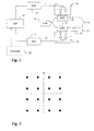
- a digital signal processor (DSP) 10 generates two digital signals, which are fed to two digital/analog converters (DAC) 11, 12.
- the analog output signals of DACs 11, 12 serve as in-phase (I) and quadrature (Q) signal components and are fed to two driver circuits 13, 14, which drive an I/Q modulator 15.
- I/Q modulator 15 modulates the laser light of a cw laser light source 16 to generate a 16-QAM signal for transmission.
- Controller 20 can be provided to adjust certain parameters of the DSP, as will be explained further below.
- Controller 20 can be implemented for example with a microprocessor or, in the most simple case, as a PID controller (proportional-integral-derivative controller).
- I/Q modulator 15 contains an interferometer structure with two branches. Mach-Zehnder modulators (MZM) 13, 74 are arranged in each of the two branches with an additional ⁇ /2 phase shifter 19 in one branch.
- Driver circuits 13, 14 generate differential drive signals I, -I and Q, -Q for MZMs 17, 18, respectively. This is indicated through an amplifier and an inverted amplifier within the driver circuits 13, 14 in figure 1 .
- an I/Q modulated optical signal will be emitted for transmission over an optical fiber link.
- the I and Q components are binary signals
- the present embodiment utilizes multi-level drive signals to support higher constellation modulation formats. This is achieved by using a DSP in combination with DACs for the I and Q branches.
- the two MZMs 17, 18 operate as amplitude modulators. Since the signals from the two branches of I/Q modulator 15 are shifted by 90° ( ⁇ /2) in optical phase, the constructive output of IJQ modulator 15 is a signal modulated in amplitude and phase, as required for x-QAM.
- the DACs have a resolution that is higher than the number of bits per symbol of each signal component (I/Q). For 16-QAM, the I and Q signal components each have 4 signal levels per symbol, i.e. 2 bit.
- the DACs hence preferably have a higher granularity of output levels and thus a resolution of more than 2 bit. In the embodiment, the DACs actually have a resolution of 6 bit, but an even higher resolution of for instance 8 bit could be envisaged.
- the higher resolution of the DAC allows to adjust the modulation levels with high precision.
- the symbol rates, at which the optical signal will be modulated are in the range of 30 GBd. More particularly, in the envisaged application, the symbol rate will be 32 GBd.
- each symbol carries 4 bit (which results in 16 constellation points).
- a rectangular constellation diagram for 16-QAM is shown by way of example in figure 2 , where I and Q signal components span a complex plane for amplitude and phase of the output signal.
- the constellation diagram in this example is rectangular, as this can be generated easily with the described modulator arrangement. It should be clear, however, that other constellations, such as hexagonal or circular constellations can be applied in the same way, by properly adjusting I and Q drive signal components.
- the DAC is operated with a sampling rate equal to the symbol rate.
- the DAC implements a digital filter function to achieve a pre-compensation of one or more component characteristics.
- the effective bandwidth characteristic of an ideal DAC follows a sinc function (sinus cardialis), i.e. the Fourier transform of a rectangular input pulse.
- sinc x sin ⁇ ⁇ x ⁇ ⁇ x .
- the I/Q modulator 15 shows a non-linear response curve. While for a multi-level signal, the highest and lowest levels are in a saturation region, the modulator shows a much higher variation of output voltage per digit at the medium levels. Thus, a precise adjustment of the modulation levels is desirable. In addition to such static behavior, the I/Q modulator 15 shows a dynamic behavior, such as for example temperature drift, so that a dynamic adjustment of the modulation levels is beneficial, too.
- driver circuits 13, 14 have a non-linear characteristic and may show a temperature dependant drift, as well, that can be compensated through proper pre-compensation.
- the DAC implements a digital filter function that pre-compensates at least one of the aforementioned component characteristics.
- the filter function is typically non-linear, the filter function can be implemented with a look-up table.
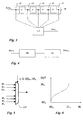
- Figure 3 shows an implementation using a look-up table LUT. Input data Data in are written to a storage device such as a shift register SR. In the shown implementation, 5 consecutive data symbols x1-x5 are considered. I and Q signal components are filtered individually and thus separate look-up tables will be provided for the two signal components, where each of the data symbols contains 2 bit per signal component.
- the data elements in the look-up table can be calculated according to a theoretical or known filter characteristic or can be determined experimentally using test patterns to adjust the DACs for the I and Q branches.
- existing DSPs operate at clock rates in the range of few GHz, but the input signal comes and must be processed at a symbol rate of 30 GBd, processing must be highly parallelized. This shows that particularly for larger symbol combinations, the look-up table implementation becomes less practical due the amount of required memory size.
- FIR filters are suited to pre-compensate for linear distortions.
- the number of parameters required for adjustment is very limited, e.g., an n-tap FIR filter requires only n tap weights.
- nonlinear filter NL is in the present embodiment a function that can be expressed as c * sin - 1 d * x - e
- the parameters c, d, and e of this function can be optimized statically or dynamically.
- the combination is this non-linear characteristics filter function NL plus an n-tap FIR filter represents a good compromise to approximate the required non-linear pre-compensation filter function.
- Figure 5 shows an implementation for the NL filter function through a simple one-dimensional look-up table LUT', which contains for each 6 bit input word 00hex - 3Fhex of I or Q (already pre-corrected through the preceding FIR filter) a corrected 6 bit output value.
- FIG. 6 An example for a correction function that can be implemented with the look-up table LUT' from figure 5 is shown in figure 6 .
- the function provides for each input value IN a corrected output value OUT.
- the correction function in figure 6 represents an inverse sine function as described above to correct for the modulator characteristic.
- FIG. 6 An improved embodiment for the filter function is shown in figure 6 . Since the size of the look-up table grows exponentially with the number of taps, the implementation shown here limits the lookup table to a subset of the elements in the center of the considered sequence of symbols and provides linear FIR filters for additional symbols farther away from the center element.
- shift register SR has seven storage locations for data elements x1-x7.
- Central data element x4 and the directly preceding and subsequent elements x3 and x5 are fed to a look-up table LUT, which implements a non-linear filter function.
- Data elements x2 and x1 are fed to a first FIR filter FIR1 and data elements x6 and x7 are fed to a second FIR filter FIR2.
- the results of look-up table LUT and FIR filters FIR1, FIR2 are added by an adder circuit ADD.
- FIR filter FIR 1 multiplies data element x1 with a weight b 0 , data element x2 with a weight b 1 and sums these up.
- FIR filter FIR 2 multiplies data element x6 with a weight b 2 , data element x7 with a weight b 3 and sums these up.
- Table 1 Example for a look-up table used in the embodiment of fig.
- modulation levels adjusted to pre-compensate for the modulator characteristics, would be: 00 bin ⁇ 00 hex 01 bin ⁇ 17 hex 10 bin ⁇ 20 hex 11 bin ⁇ 3 ⁇ F hex
- the output from adder circuit ADD can optionally feed to another non-linear filter function NL such as the filter function show in figures 5 and 6 . This allows to separate influences from different circuit components of the transmitter and thus permits simplified dynamic adjustment of filter characteristics.
- FIG 8 An extension of the optical transmitter from figure 1 applying polarization division multiplexing is shown in figure 8 .
- the cw laser light from a laser 16' is split through polarization beam splitter 8 in two orthogonal polarization components, each of which is fed to a QAM transmitter QAM1, QAM2 similar to the one shown in figure 1 (with laser 16 from figure 1 replaced through laser 16' in figure 8 ).
- the output of the two QAM transmitters is combined and transmitted over a fiber link.
- Figure 9 shows an optical receiver using coherent signal detection.
- the received optical signal arrives at receiver input IN.
- a 3 dB splitter splits the received optical signal and connects to two optical hybrids H1, H2, which serve as I/Q couplers.
- a tunable cw laser L serves as local oscillator.
- a polarization splitter PS splits the output signal of laser L in two orthogonal polarization components, one for each optical hybrid H1, H2. Since the optical hybrid is polarization sensitive, the two hybrids will deliver I and Q components in different polarization states of the input signal.
- Each optical hybrid H1, H2 has two outputs for down-converted raw in-phase and quadrature signal components.
- Each signal component is fed to a photodiode acting as O/E converted and digitized using a ADC operating at a sampling rate above the symbol rate.
- the four digitized signals are fed to a signal processor DSP, which recovers the signals and delivers expectation values for the I and Q signal components of the transmitted data signals in the two orthogonal polarization states.
- the signal processing includes compensation of chromatic dispersion and polarization mode dispersion, carrier phase recovery, frequency offset compensation, and non-linear compensation.
- the processing of the received signals to recover the data signals is known per se and described for example in the paper " Digital Signal Processing Algorithms for High-Speed Coherent Transmission in Optical Fibers" by M. Mussolini, University of Padua 2010 , which is incorporated by reference herein.
- the receiver contains a monitor M, which monitors certain characteristics of the received signal available at the digital signal processor DSP and provides these characteristics via a backchannel to the transmitter to support adjustment of filter parameters at the pre-compensation stage in the transmitter.
- the backchannel can be an overhead byte in the reverse direction of a bidirectional link or can use any other kind of communication, including control plane or management plane communication.
- Transmitters Tx and receivers Rx are usually grouped to transponders for bidirectional optical signal transmission.
- a transmitter in transponder 1 contains a pre-compensation stage as explained in the embodiments before.
- a receiver Rx at transponder 2 contains a monitor, which measures the constellation diagram of the received signal. This can be easily accomplished by averaging over the expectation values for the different signal values 0-3 of the I and Q signal components.
- the constellation diagram shows a deviation of the two inner amplitude levels of the I component with respect to nominal equidistant amplitude levels.
- This measured deviation is signaled back to transmitter Tx in transponder 1, where it is used to adjust the modulation levels of the modulator by appropriate pre-compensation at the DSP, e.g. through adjustment of a filter function that compensates for the non-linear modulator characteristics.
- adjustment of the filter parameters is accomplished through a controller in transmitter Tx, for example controller 20 in figure 1 .
- test patterns can be applied. To distinguish between I and Q branch and adjust both independantly, different patterns can be used for the two branches. In the monitor, the mean values of the received symbol combinations can be calculated and fed back to the transmitter.
- the Tx settings may be applied as static parameter sets or may be adjusted dynamically. Dynamic adjustment is advantageous because the optimum settings may depend on temperature dependent drift of drivers, modulator bias etc..
- the receiver performs digital signal processing to remove signal distortions through chromatic dispersion and polarization mode dispersion.
- part of such distortion compensation can be achieved through pre-filtering in the transmitter. Distortion compensation can therefore be shared between the digital signal pre-compensation in the transmitter and distortion compensation through digital signal processing in the receiver.
- the distortion compensation is shared such that the transmitter pre-compensates for distortion occurring over roughly the first half of the transmission distance and the receiver compensates for distortions assembled along the remainder of the transmission distance. After about half of the transmission distance, the optical signal would hence have a shape and waveform of an undistorted signal.
- the data signal DATA is subject to digital pre-compensation using a filter function 101, implemented using a look-up table LUT alone or in combination with a FIR filter.
- the pre-compensated data values drive through a DAC (not shown) an I/Q modulator 102.
- a controller 103 implemented using for example a ⁇ Processor or a PID, provides a DC bias voltage for I/Q modulator 102.
- the DC bias serves to adjust the operating point of the I/Q modulator, as it is known per se to those skilled in the art.
- a low frequency dither tone from a NF source 104 is added to the bias signal for monitoring purpose.
- the optical signal output from I/Q modulator 102 is branched as a feedback control to a O/E converter 105, a filter circuit 106, which selects the NF dither tone, and an integrator 107 to generate a feedback signal for controller 103 to adjust the DC bias voltage.
- controller 103 not only adjusts the DC bias voltage for I/Q modulator 102, but also adjusts filter parameters such as the modulation levels in the DSP that performs the digital pre-compensation function 101.
- processors may be provided through the use of dedicated hardware as well as hardware capable of executing software in association with appropriate software.
- the functions may be provided by a single dedicated processor, by a single shared processor, or by a plurality of individual processors, some of which may be shared.
- explicit use of the term "processor” or “controller” should not be construed to refer exclusively to hardware capable of executing software, and may implicitly include, without limitation, digital signal processor (DSP) hardware, network processor, application specific integrated circuit (ASIC), field programmable gate array (FPGA), read only memory (ROM) for storing software, random access memory (RAM), and non volatile storage.
- DSP digital signal processor
- ASIC application specific integrated circuit
- FPGA field programmable gate array
- ROM read only memory
- RAM random access memory
- non volatile storage Other hardware, conventional and/or custom, may also be included.
Landscapes
- Physics & Mathematics (AREA)
- Electromagnetism (AREA)
- Engineering & Computer Science (AREA)
- Computer Networks & Wireless Communication (AREA)
- Signal Processing (AREA)
- Optics & Photonics (AREA)
- Optical Communication System (AREA)
Abstract
Description
- The present invention relates to the field of telecommunications and more particularly to a transmitter for high bitrate optical data transmission.
- In optical transmission networks, the amount of data to be transmitted is ever increasing, thus leading to higher bitrates and the development of system with higher spectral efficiency. Wavelength division multiplexing is used to transmit a plurality of data signals at different carrier wavelengths over an standard single-mode optical fiber. A further degree of freedom that can be utilized is the signal polarization, so that signals at the same wavelength but having orthogonal polarization can be transmitted in parallel over a fiber.
- Today, systems are available that can transport 100 Gb/s signals per wavelength using a combination of QPSK modulation (quadrature phase-shift keying) and polarization multiplexing. The use of higher constellation modulation schemes such 16-QAM (quadrature amplitude modulation) has been proposed, which involves modulation of phase and amplitude. However, commercially applicable transmitters for optical x-QAM do not exist so far.
- It is therefore an object of the present invention to provide an optical transmitter that allows reliable QAM transmission.
- These and other objects that appear below are achieved by an optical transmitter, which contains a digital signal processor coupled to a digital-to-analog converter for generating multi-level drive signals; and an I/Q modulator for modulating an optical carrier signal with the drive signals to generate a quadrature amplitude modulated optical signal. The digital signal processor performs at least one digital filter function on data elements to be transmitted to pre-compensate for a non-linear characteristic of at least one circuit component of the optical transmitter causing distortions in said quadrature amplitude modulated optical signal.
- The present embodiments provide a solution with a high spectral efficiency, improved performance and increased the transmission reach.
- Preferred embodiments of the present invention will now be described with reference to the accompanying drawings in which
- figure 1
- shows a block diagram of an optical transmitter in an embodiment;
- figure 2
- shows a constellation diagram of 16-QAM;
- figure 3
- shows an first embodiment of a digital pre-filter stage that can be implemented into an DSP;
- figure 4
- shows a second embodiment of a digital pre-filter stage;
- figure 5
- shows a look-up table that can be used to perform a non-linear filter function within a DSP;
- figure 6
- shows a characteristic curve of an I/Q modulator;
- figure 7
- shows a third embodiment of a digital pre-filter stage;
- figure 8
- shows a transmitter applying polarization multiplexing;
- figure 9
- shows an embodiment of an optical receiver for coherent detection, which can be utilized to adjust filter parameters in the optical transmitter;
- figure 10
- shows an embodiment for a signaling of parameters measured at a receiver via a feedback channel; and
- figure 11
- sows a further embodiment of an optical transmitter.
- An embodiment of an optical transmitter suitable to generate x-QAM signals is shown schematically in
figure 1 . A digital signal processor (DSP) 10 generates two digital signals, which are fed to two digital/analog converters (DAC) 11, 12. The analog output signals ofDACs driver circuits Q modulator 15. I/Q modulator 15 modulates the laser light of a cwlaser light source 16 to generate a 16-QAM signal for transmission. - An
optional controller 20 can be provided to adjust certain parameters of the DSP, as will be explained further below.Controller 20 can be implemented for example with a microprocessor or, in the most simple case, as a PID controller (proportional-integral-derivative controller). - I/
Q modulator 15 contains an interferometer structure with two branches. Mach-Zehnder modulators (MZM) 13, 74 are arranged in each of the two branches with an additional π/2phase shifter 19 in one branch.Driver circuits MZMs driver circuits figure 1 . - At the constructive output of the I/
Q modulator 15, an I/Q modulated optical signal will be emitted for transmission over an optical fiber link. - While for the generation of a QPSK modulated signal, the I and Q components are binary signals, only, the present embodiment utilizes multi-level drive signals to support higher constellation modulation formats. This is achieved by using a DSP in combination with DACs for the I and Q branches.
- The two
MZMs Q modulator 15 are shifted by 90° (π/2) in optical phase, the constructive output ofIJQ modulator 15 is a signal modulated in amplitude and phase, as required for x-QAM. - The DACs have a resolution that is higher than the number of bits per symbol of each signal component (I/Q). For 16-QAM, the I and Q signal components each have 4 signal levels per symbol, i.e. 2 bit. The DACs hence preferably have a higher granularity of output levels and thus a resolution of more than 2 bit. In the embodiment, the DACs actually have a resolution of 6 bit, but an even higher resolution of for
instance 8 bit could be envisaged. The higher resolution of the DAC allows to adjust the modulation levels with high precision. - The symbol rates, at which the optical signal will be modulated are in the range of 30 GBd. More particularly, in the envisaged application, the symbol rate will be 32 GBd. For 16-QAM, each symbol carries 4 bit (which results in 16 constellation points). A rectangular constellation diagram for 16-QAM is shown by way of example in
figure 2 , where I and Q signal components span a complex plane for amplitude and phase of the output signal. The constellation diagram in this example is rectangular, as this can be generated easily with the described modulator arrangement. It should be clear, however, that other constellations, such as hexagonal or circular constellations can be applied in the same way, by properly adjusting I and Q drive signal components. - As signals can be transmitted at two orthogonal states of polarization, another factor of 2 comes into play. With a symbol rate of 32 GBd, this results in a total data rate of 2 * 4 bit * 32 GBd = 256 Gbit/s, which would be sufficient to transport a 200 Gbit/s data signal plus overhead and FEC frame per wavelength using a 50 GHz DWDM wavelength grid.
- In the subject embodiment, the DAC is operated with a sampling rate equal to the symbol rate. However, it may be beneficial to apply a higher sampling rate, i.e. oversampling, to generate even better analog drive signal waveforms for the I/Q modulator.
- At the envisaged high symbol rates, several effects and limitations of the electrical and optical components of the transmitter will affect the output signal and lead to non-linear signal distortions. Therefore, the DAC implements a digital filter function to achieve a pre-compensation of one or more component characteristics.
- The effective bandwidth characteristic of an ideal DAC follows a sinc function (sinus cardialis), i.e. the Fourier transform of a rectangular input pulse. In digital signal processing, the normalized sinc function is commonly defined by

- Due to this theoretical bandwidth characteristic, a D/A converted output signal is degraded even in an ideal DAC and would not follow the shape of a rectangular input pulse.
- In addition to the theoretical bandwidth characteristic of an ideal DAC, real DACs further show a bandwidth limitation towards higher frequencies, which will become relevant at the envisaged symbol rates. A further limitation of DACs, as available today, is an asymmetry due to different speeds for switching an output signal on and off.
- Further to this, the I/
Q modulator 15 shows a non-linear response curve. While for a multi-level signal, the highest and lowest levels are in a saturation region, the modulator shows a much higher variation of output voltage per digit at the medium levels. Thus, a precise adjustment of the modulation levels is desirable. In addition to such static behavior, the I/Q modulator 15 shows a dynamic behavior, such as for example temperature drift, so that a dynamic adjustment of the modulation levels is beneficial, too. - Furthermore, the
driver circuits - For these reasons, the DAC implements a digital filter function that pre-compensates at least one of the aforementioned component characteristics. As due to the component characteristic, the filter function is typically non-linear, the filter function can be implemented with a look-up table.
Figure 3 shows an implementation using a look-up table LUT. Input data Datain are written to a storage device such as a shift register SR. In the shown implementation, 5 consecutive data symbols x1-x5 are considered. I and Q signal components are filtered individually and thus separate look-up tables will be provided for the two signal components, where each of the data symbols contains 2 bit per signal component. - The individual 2 bit symbol components are fed as address values to the look-up table LUT, which contains 6 bit wide output values for any possible input symbol combinations. This output value is then read and sent as output signal Dataout. Considering in
figure 3 data symbol x3 (n=3) as the current element, it becomes clear that the filter algorithm takes into account contributions from the direct neighboring elements n±1 and the next adjacent elements n±2. - The data elements in the look-up table can be calculated according to a theoretical or known filter characteristic or can be determined experimentally using test patterns to adjust the DACs for the I and Q branches.
- In the embodiment of
figure 3 , look-up table LUT contains 45 = 1024 data values of 6 bit for I and Q, each. As existing DSPs operate at clock rates in the range of few GHz, but the input signal comes and must be processed at a symbol rate of 30 GBd, processing must be highly parallelized. This shows that particularly for larger symbol combinations, the look-up table implementation becomes less practical due the amount of required memory size. - Therefore, a combination of a finite impulse response (FIR) filter and filter with non-linear characteristics NL, as shown schematically in
figure 4 , is a good alternative. FIR filters are suited to pre-compensate for linear distortions. The number of parameters required for adjustment is very limited, e.g., an n-tap FIR filter requires only n tap weights. - In addition a nonlinear characteristic is required to compensate for the sine function of the modulator and for the soft clipping/limitation of the DAC and driver amplifier. The curve applied by non-linear filter NL is in the present embodiment a function that can be expressed as

- The parameters c, d, and e of this function can be optimized statically or dynamically. The combination is this non-linear characteristics filter function NL plus an n-tap FIR filter represents a good compromise to approximate the required non-linear pre-compensation filter function.
-
Figure 5 shows an implementation for the NL filter function through a simple one-dimensional look-up table LUT', which contains for each 6 bit input word 00hex - 3Fhex of I or Q (already pre-corrected through the preceding FIR filter) a corrected 6 bit output value. - An example for a correction function that can be implemented with the look-up table LUT' from
figure 5 is shown infigure 6 . The function provides for each input value IN a corrected output value OUT. The correction function infigure 6 represents an inverse sine function as described above to correct for the modulator characteristic. - An improved embodiment for the filter function is shown in
figure 6 . Since the size of the look-up table grows exponentially with the number of taps, the implementation shown here limits the lookup table to a subset of the elements in the center of the considered sequence of symbols and provides linear FIR filters for additional symbols farther away from the center element. - In this embodiment, shift register SR has seven storage locations for data elements x1-x7. Central data element x4 and the directly preceding and subsequent elements x3 and x5 are fed to a look-up table LUT, which implements a non-linear filter function. Data elements x2 and x1 are fed to a first FIR filter FIR1 and data elements x6 and x7 are fed to a second FIR filter FIR2. The results of look-up table LUT and FIR filters FIR1, FIR2 are added by an adder circuit ADD.
-
FIR filter FIR 1 multiplies data element x1 with a weight b0, data element x2 with a weight b1 and sums these up. Similarly,FIR filter FIR 2 multiplies data element x6 with a weight b2, data element x7 with a weight b3 and sums these up. An example for a look-up table used in the embodiment is shown in table 1 below.Table 1: Example for a look-up table used in the embodiment of fig. 6 x5=0 x5=1 x5=2 x5=3 x4=0 x3=0 17 13 11 8 x3 =1 14 11 9 5 x3=2 12 8 6 3 x3=3 9 6 3 0 x4=1 x3=0 32 29 27 24 x3=1 30 27 25 21 x3=2 28 24 22 19 x3=3 25 22 19 16 x4=2 x3=0 47 44 42 38 x3=1 45 42 39 36 x3=2 42 39 37 34 x3=3 40 36 34 31 x4=3 x3=0 63 60 57 54 x3=1 61 57 55 52 x3=2 58 55 53 49 x3=3 55 52 50 46 - An example for modulation levels, adjusted to pre-compensate for the modulator characteristics, would be:

- The output from adder circuit ADD can optionally feed to another non-linear filter function NL such as the filter function show in
figures 5 and 6 . This allows to separate influences from different circuit components of the transmitter and thus permits simplified dynamic adjustment of filter characteristics. - An extension of the optical transmitter from
figure 1 applying polarization division multiplexing is shown infigure 8 . The cw laser light from a laser 16' is split throughpolarization beam splitter 8 in two orthogonal polarization components, each of which is fed to a QAM transmitter QAM1, QAM2 similar to the one shown infigure 1 (withlaser 16 fromfigure 1 replaced through laser 16' infigure 8 ). The output of the two QAM transmitters is combined and transmitted over a fiber link. -
Figure 9 shows an optical receiver using coherent signal detection. The received optical signal arrives at receiver input IN. A 3 dB splitter splits the received optical signal and connects to two optical hybrids H1, H2, which serve as I/Q couplers. A tunable cw laser L serves as local oscillator. A polarization splitter PS splits the output signal of laser L in two orthogonal polarization components, one for each optical hybrid H1, H2. Since the optical hybrid is polarization sensitive, the two hybrids will deliver I and Q components in different polarization states of the input signal. - Each optical hybrid H1, H2 has two outputs for down-converted raw in-phase and quadrature signal components. Each signal component is fed to a photodiode acting as O/E converted and digitized using a ADC operating at a sampling rate above the symbol rate. The four digitized signals are fed to a signal processor DSP, which recovers the signals and delivers expectation values for the I and Q signal components of the transmitted data signals in the two orthogonal polarization states.
- The signal processing includes compensation of chromatic dispersion and polarization mode dispersion, carrier phase recovery, frequency offset compensation, and non-linear compensation. The processing of the received signals to recover the data signals is known per se and described for example in the paper "Digital Signal Processing Algorithms for High-Speed Coherent Transmission in Optical Fibers" by M. Mussolini, University of Padua 2010, which is incorporated by reference herein.
- According to an embodiments, the receiver contains a monitor M, which monitors certain characteristics of the received signal available at the digital signal processor DSP and provides these characteristics via a backchannel to the transmitter to support adjustment of filter parameters at the pre-compensation stage in the transmitter. The backchannel can be an overhead byte in the reverse direction of a bidirectional link or can use any other kind of communication, including control plane or management plane communication.
- An embodiment of such monitoring is shown in
figure 9 . Transmitters Tx and receivers Rx are usually grouped to transponders for bidirectional optical signal transmission. A transmitter intransponder 1 contains a pre-compensation stage as explained in the embodiments before. A receiver Rx attransponder 2 contains a monitor, which measures the constellation diagram of the received signal. This can be easily accomplished by averaging over the expectation values for the different signal values 0-3 of the I and Q signal components. In the embodiment, the constellation diagram shows a deviation of the two inner amplitude levels of the I component with respect to nominal equidistant amplitude levels. This measured deviation is signaled back to transmitter Tx intransponder 1, where it is used to adjust the modulation levels of the modulator by appropriate pre-compensation at the DSP, e.g. through adjustment of a filter function that compensates for the non-linear modulator characteristics. Such adjustment of the filter parameters is accomplished through a controller in transmitter Tx, forexample controller 20 infigure 1 . - In order to adjust the DACs of the transmitter for I and Q branches, test patterns can be applied. To distinguish between I and Q branch and adjust both independantly, different patterns can be used for the two branches. In the monitor, the mean values of the received symbol combinations can be calculated and fed back to the transmitter. The Tx settings may be applied as static parameter sets or may be adjusted dynamically. Dynamic adjustment is advantageous because the optimum settings may depend on temperature dependent drift of drivers, modulator bias etc..
- Use of this dynamic pre-compensation enables to operate the system at optimum performance for fiber tranmsision in linear regime. Typically optical transmission systems are operated close to the nonlinear threshold. A further improvement of the nonlinear threshold can be obtained through an additional pre-filtering of transmission impairments along the optical fiber.
- As explained above, the receiver performs digital signal processing to remove signal distortions through chromatic dispersion and polarization mode dispersion. However, in an advantageous embodiment, part of such distortion compensation can be achieved through pre-filtering in the transmitter. Distortion compensation can therefore be shared between the digital signal pre-compensation in the transmitter and distortion compensation through digital signal processing in the receiver.
- Advantageously, the distortion compensation is shared such that the transmitter pre-compensates for distortion occurring over roughly the first half of the transmission distance and the receiver compensates for distortions assembled along the remainder of the transmission distance. After about half of the transmission distance, the optical signal would hence have a shape and waveform of an undistorted signal.
- Another embodiment of a dynamic adjustment of filter parameters in the transmitter is shown in
figure 10 . The data signal DATA is subject to digital pre-compensation using a filter function 101, implemented using a look-up table LUT alone or in combination with a FIR filter. The pre-compensated data values drive through a DAC (not shown) an I/Q modulator 102. A controller 103, implemented using for example a µProcessor or a PID, provides a DC bias voltage for I/Q modulator 102. The DC bias serves to adjust the operating point of the I/Q modulator, as it is known per se to those skilled in the art. A low frequency dither tone from a NF source 104 is added to the bias signal for monitoring purpose. The optical signal output from I/Q modulator 102 is branched as a feedback control to a O/E converter 105, a filter circuit 106, which selects the NF dither tone, and an integrator 107 to generate a feedback signal for controller 103 to adjust the DC bias voltage. - According to an aspect of this embodiment, controller 103 not only adjusts the DC bias voltage for I/Q modulator 102, but also adjusts filter parameters such as the modulation levels in the DSP that performs the digital pre-compensation function 101.
- Although described for 16-QAM modulation, it should be understood that the present embodiments can also be applied to 64-QAM, 256-QAM or even higher constellations. The higher the number of constellations, the shorter the achievable transmission distance, however. Advanced FEC coding can be applied hence to increase the transmission distance.
- The functions of the various elements shown in the figures, including any functional blocks labeled as "processors", may be provided through the use of dedicated hardware as well as hardware capable of executing software in association with appropriate software. When provided by a processor, the functions may be provided by a single dedicated processor, by a single shared processor, or by a plurality of individual processors, some of which may be shared. Moreover, explicit use of the term "processor" or "controller" should not be construed to refer exclusively to hardware capable of executing software, and may implicitly include, without limitation, digital signal processor (DSP) hardware, network processor, application specific integrated circuit (ASIC), field programmable gate array (FPGA), read only memory (ROM) for storing software, random access memory (RAM), and non volatile storage. Other hardware, conventional and/or custom, may also be included.
- The description and drawings merely illustrate the principles of the invention. It will thus be appreciated that those skilled in the art will be able to devise various arrangements that, although not explicitly described or shown herein, embody the principles of the invention. Furthermore, all examples recited herein are principally intended expressly to be only for pedagogical purposes to aid the reader in understanding the principles of the invention and the concepts contributed by the inventors to furthering the art, and are to be construed as being without limitation to such specifically recited examples and conditions. Moreover, all statements herein reciting principles, aspects, and embodiments of the invention, as well as specific examples thereof, are intended to encompass equivalents thereof.
Claims (15)
- An optical transmitter, comprising a digital signal processor (10) coupled to a digital-to-analog converter (11, 12) for generating multi-level drive signals; and an I/Q modulator (15) for modulating an optical carrier signal with said drive signals to generate a quadrature amplitude modulated optical signal; wherein said digital signal processor (10) is adapted to perform at least one digital filter function (LUT, FIR, NL) on data elements to be transmitted to pre-compensate for a non-linear characteristic of at least one circuit component of said optical transmitter causing distortions in said quadrature amplitude modulated optical signal.
- An optical transmitter according to claim 1, wherein said digital filter function comprises a function performed on a sequence of consecutive data elements (x1-x5; x1-x7),
- An optical transmitter according to claim 1, wherein said digital filter function comprises a look-up table (LUT, LUT).
- An optical transmitter according to claim 1, wherein said digital filter function comprises a look-up table (LUT') in combination with a finite impulse response filter (FIR1, FIR2).
- An optical transmitter according to claim 2 and 4, wherein said look-up table (LUT') is applied to one or more inner data elements (x3-x5) of said sequence and wherein said finite impulse response filter (FIR1, FIR2) is applied to two or more outer data elements (x1, x2, x6, x7) of said sequence.
- An optical transmitter according to claim 1, wherein said digital-to-analog converter (11, 12) has a resolution higher than the number of bits per symbol of each drive signal.
- An optical transmitter according to claim 1, wherein said digital signal processor (10) is adapted to additionally perform a second digital filter function to pre-compensate for linear distortions of the optical signal during transmission over a part of an optical fiber link.
- An optical transmitter according to claim 1, further comprising a controller (20) adapted to adjust filter parameters within said digital signal processor (10).
- An optical transmitter according to claim 8, wherein said controller (20) is adapted to receive via a feedback channel information about signal characteristics determined at a remote optical receiver (Rx) and to determine said parameters from said received information.
- An optical transmitter according to claim 1, wherein said non-linear component characteristic includes any of a bandwidth characteristic of said digital to analog converter (11, 12), a non-linear response curve of said I/Q modulator (15), and a non-linear characteristic of driver amplifiers 13, 14) provided to drive said I/Q modulator (15) with said drive signals.
- A method of transmitting a data signal over an optical fiber link; comprising generating multi-level drive signals using a digital signal processor (10) coupled to a digital-to-analog converter (11, 12), and modulating an optical carrier signal with said drive signals using an I/Q modulator (15) to generate a quadrature amplitude modulated optical signal for transmission; further comprising performing at least one digital filter function (LUT, NL, FIR) on data elements (x1-x7) to be transmitted to pre-compensate for a non-linear characteristic of at least one circuit component of said optical transmitter causing distortions in said quadrature amplitude modulated optical signal.
- A method according to claim 11, further comprising, at a remote receiver (Rx), processing said optical signal to determine characteristics of the received signal; transmitting said characteristics via a return channel to the optical transmitter (Tx); and at the optical transmitter, determining from said characteristics adjustments to filter parameters of said digital filter function (LUT, NL, FIR).
- A method according to claim 12, wherein said characteristics comprise deviations of constellation points in a measured constellation diagram from nominal values.
- A method according to claim 12, comprising modulating in the optical transmitter (Tx) said optical carrier with test patterns to determine adjustments of said filter parameters in the optical receiver (Rx).
- A coherent optical receiver, comprising a local oscillator (L) and an I/Q coupler (H1, H2) for mixing a received quadrature amplitude modulated optical signal (IN) with a local oscillator signal to produce phase and amplitude components of said received optical signal; O/E converters (PD) and analog-to-digital converters (ADC) for sampling said phase and amplitude components and a digital signal processor (DSP) for processing said sampled signals to recover in-phase and quadrature components of a transmitted data signal; further comprising a monitor (M) for determining characteristics of the received optical signal (IN); and transmitting said characteristics via a return channel to a remote optical transmitter (Tx) to support adjustment of filter parameters at said optical transmitter (Tx) used to pre-compensate for a non-linear characteristic of at least one circuit component of said optical transmitter (Tx) causing distortions in said quadrature amplitude modulated optical signal.
Priority Applications (1)
| Application Number | Priority Date | Filing Date | Title |
|---|---|---|---|
| EP12305035.3A EP2634934B1 (en) | 2012-01-10 | 2012-01-10 | Optical transmitter |
Applications Claiming Priority (1)
| Application Number | Priority Date | Filing Date | Title |
|---|---|---|---|
| EP12305035.3A EP2634934B1 (en) | 2012-01-10 | 2012-01-10 | Optical transmitter |
Publications (2)
| Publication Number | Publication Date |
|---|---|
| EP2634934A1 true EP2634934A1 (en) | 2013-09-04 |
| EP2634934B1 EP2634934B1 (en) | 2016-05-04 |
Family
ID=45509408
Family Applications (1)
| Application Number | Title | Priority Date | Filing Date |
|---|---|---|---|
| EP12305035.3A Not-in-force EP2634934B1 (en) | 2012-01-10 | 2012-01-10 | Optical transmitter |
Country Status (1)
| Country | Link |
|---|---|
| EP (1) | EP2634934B1 (en) |
Cited By (8)
| Publication number | Priority date | Publication date | Assignee | Title |
|---|---|---|---|---|
| US20150117869A1 (en) * | 2013-10-31 | 2015-04-30 | Hitachi, Ltd. | Optical multilevel transmitter and optical transponder |
| EP2975788A3 (en) * | 2014-07-16 | 2016-04-20 | Fujitsu Limited | Optical transmission apparatus and detection apparatus |
| WO2016078705A1 (en) * | 2014-11-20 | 2016-05-26 | Telefonaktiebolaget L M Ericsson (Publ) | Method of controlling the generation of a coherent optical signal and coherent optical signal control apparatus |
| JP2018087846A (en) * | 2016-11-28 | 2018-06-07 | 日本電気株式会社 | Optical modulation device and method for controlling optical modulator |
| CN108847886A (en) * | 2018-05-25 | 2018-11-20 | 复旦大学 | A kind of method for transmitting signals of space division multiplexing mode |
| JPWO2021199317A1 (en) * | 2020-03-31 | 2021-10-07 | ||
| US11271366B2 (en) | 2014-04-25 | 2022-03-08 | Semtech Canada Corporation | Non-linear filter for DML |
| WO2022269782A1 (en) * | 2021-06-23 | 2022-12-29 | 日本電信電話株式会社 | Optical transmission system, transmission apparatus, reception apparatus, and device characteristic estimation method |
Citations (1)
| Publication number | Priority date | Publication date | Assignee | Title |
|---|---|---|---|---|
| US7826752B1 (en) * | 2005-06-02 | 2010-11-02 | Level 3 Communications, Llc | Optical transmission apparatuses, methods, and systems |
-
2012
- 2012-01-10 EP EP12305035.3A patent/EP2634934B1/en not_active Not-in-force
Patent Citations (1)
| Publication number | Priority date | Publication date | Assignee | Title |
|---|---|---|---|---|
| US7826752B1 (en) * | 2005-06-02 | 2010-11-02 | Level 3 Communications, Llc | Optical transmission apparatuses, methods, and systems |
Non-Patent Citations (1)
| Title |
|---|
| MORIYA NAKAMURA ET AL: "Experimental demonstration of 16-QAM transmission with a single dual-drive Mach-Zehnder modulator", OPTICAL FIBER COMMUNICATION CONFERENCE, 2011. TECHNICAL DIGEST. OFC/NFOEC, IEEE, 6 March 2011 (2011-03-06), pages 1 - 3, XP031946042, ISBN: 978-1-4577-0213-6 * |
Cited By (16)
| Publication number | Priority date | Publication date | Assignee | Title |
|---|---|---|---|---|
| JP2015088999A (en) * | 2013-10-31 | 2015-05-07 | 株式会社日立製作所 | Optical multilevel transmitter and optical transponder |
| US20150117869A1 (en) * | 2013-10-31 | 2015-04-30 | Hitachi, Ltd. | Optical multilevel transmitter and optical transponder |
| US11271366B2 (en) | 2014-04-25 | 2022-03-08 | Semtech Canada Corporation | Non-linear filter for DML |
| US11664639B2 (en) | 2014-04-25 | 2023-05-30 | Semtech Canada Corporation | Device having non-linear filter |
| EP2975788A3 (en) * | 2014-07-16 | 2016-04-20 | Fujitsu Limited | Optical transmission apparatus and detection apparatus |
| US9667344B2 (en) | 2014-07-16 | 2017-05-30 | Fujitsu Limited | Optical transmission apparatus and detection apparatus |
| WO2016078705A1 (en) * | 2014-11-20 | 2016-05-26 | Telefonaktiebolaget L M Ericsson (Publ) | Method of controlling the generation of a coherent optical signal and coherent optical signal control apparatus |
| US10056980B2 (en) | 2014-11-20 | 2018-08-21 | Telefonaktiebolaget Lm Ericsson (Publ) | Method of controlling the generation of a coherent optical signal and coherent optical signal control apparatus |
| JP2018087846A (en) * | 2016-11-28 | 2018-06-07 | 日本電気株式会社 | Optical modulation device and method for controlling optical modulator |
| CN108847886A (en) * | 2018-05-25 | 2018-11-20 | 复旦大学 | A kind of method for transmitting signals of space division multiplexing mode |
| JPWO2021199317A1 (en) * | 2020-03-31 | 2021-10-07 | ||
| WO2021199317A1 (en) * | 2020-03-31 | 2021-10-07 | 日本電信電話株式会社 | Optical transmission system and characteristic estimation method |
| WO2022269782A1 (en) * | 2021-06-23 | 2022-12-29 | 日本電信電話株式会社 | Optical transmission system, transmission apparatus, reception apparatus, and device characteristic estimation method |
| JPWO2022269782A1 (en) * | 2021-06-23 | 2022-12-29 | ||
| JP7530026B2 (en) | 2021-06-23 | 2024-08-07 | 日本電信電話株式会社 | Optical transmission system, transmitter, receiver, and device characteristic estimation method |
| EP4362356A4 (en) * | 2021-06-23 | 2025-04-30 | Nippon Telegraph And Telephone Corporation | OPTICAL TRANSMISSION SYSTEM, TRANSMISSION DEVICE, RECEIVING DEVICE AND METHOD FOR ESTIMATING DEVICE CHARACTERISTICS |
Also Published As
| Publication number | Publication date |
|---|---|
| EP2634934B1 (en) | 2016-05-04 |
Similar Documents
| Publication | Publication Date | Title |
|---|---|---|
| EP2634934B1 (en) | Optical transmitter | |
| US10225017B2 (en) | Optical transmitter and method for controlling the same | |
| US9853725B2 (en) | Optical dispersion compensation in the electrical domain in an optical communications system | |
| CN102282784B (en) | Optical transmitter | |
| EP1943755B1 (en) | Methods and apparatus for optical transmission of digital signals | |
| EP2896988B1 (en) | Optical transmitter and dc bias control method | |
| US8681027B2 (en) | Digital receiver and optical communication system that uses same | |
| Che et al. | 2.4-Tb/s single-wavelength coherent transmission enabled by 114-GHz all-electronic digital-band-interleaved DACs | |
| US8948609B2 (en) | Pre-distortion techniques for optical modulators to improve constellation point separation | |
| JP2011232553A (en) | Optical transmitter, optical communication system and modulation method | |
| US11336367B1 (en) | Low-power pre-compensation of linear and nonlinear transmitter effects in narrow-spectrum optical signals | |
| Erkılınç et al. | Spectrally efficient WDM Nyquist pulse-shaped subcarrier modulation using a dual-drive Mach–Zehnder modulator and direct detection | |
| US9787403B2 (en) | Digital optical transmitter, optical communication system using the same, and digital optical transmission method | |
| JP5289428B2 (en) | Digital signal processing optical transmitter | |
| JP6350762B2 (en) | Optical transmitter and optical communication method | |
| CA3176508C (en) | Low-power pre-compensation of linear and nonlinear transmitter effects in narrow-spectrum optical signals | |
| WO2013128835A1 (en) | Optical receiver and optical communication system | |
| JP2023148267A (en) | Nonlinear compensation circuit and optical transceiver | |
| Josten et al. | Amplifiers-Optimal Operation Conditions | |
| Ragheb et al. | Investigation of sampling frequency impact on optical DP‐MQAM generation | |
| BR102014016378A2 (en) | multiobjective method of optimizing digital pre-equalizer filters for optical communication systems | |
| HK1122146B (en) | Methods and apparatus for optical transmission of digital signals |
Legal Events
| Date | Code | Title | Description |
|---|---|---|---|
| PUAI | Public reference made under article 153(3) epc to a published international application that has entered the european phase |
Free format text: ORIGINAL CODE: 0009012 |
|
| 17P | Request for examination filed |
Effective date: 20120806 |
|
| AK | Designated contracting states |
Kind code of ref document: A1 Designated state(s): AL AT BE BG CH CY CZ DE DK EE ES FI FR GB GR HR HU IE IS IT LI LT LU LV MC MK MT NL NO PL PT RO RS SE SI SK SM TR |
|
| AX | Request for extension of the european patent |
Extension state: BA ME |
|
| RBV | Designated contracting states (corrected) |
Designated state(s): AL AT BE BG CH CY CZ DE DK EE ES FI FR GB GR HR HU IE IS IT LI LT LU LV MC MK MT NL NO PL PT RO RS SE SI SK SM TR |
|
| RAP1 | Party data changed (applicant data changed or rights of an application transferred) |
Owner name: ALCATEL LUCENT |
|
| RIC1 | Information provided on ipc code assigned before grant |
Ipc: H04B 10/50 20130101AFI20150421BHEP |
|
| 17Q | First examination report despatched |
Effective date: 20150730 |
|
| GRAP | Despatch of communication of intention to grant a patent |
Free format text: ORIGINAL CODE: EPIDOSNIGR1 |
|
| INTG | Intention to grant announced |
Effective date: 20160107 |
|
| GRAS | Grant fee paid |
Free format text: ORIGINAL CODE: EPIDOSNIGR3 |
|
| GRAA | (expected) grant |
Free format text: ORIGINAL CODE: 0009210 |
|
| AK | Designated contracting states |
Kind code of ref document: B1 Designated state(s): AL AT BE BG CH CY CZ DE DK EE ES FI FR GB GR HR HU IE IS IT LI LT LU LV MC MK MT NL NO PL PT RO RS SE SI SK SM TR |
|
| REG | Reference to a national code |
Ref country code: GB Ref legal event code: FG4D |
|
| REG | Reference to a national code |
Ref country code: CH Ref legal event code: EP |
|
| REG | Reference to a national code |
Ref country code: AT Ref legal event code: REF Ref document number: 797714 Country of ref document: AT Kind code of ref document: T Effective date: 20160515 |
|
| REG | Reference to a national code |
Ref country code: IE Ref legal event code: FG4D |
|
| REG | Reference to a national code |
Ref country code: DE Ref legal event code: R096 Ref document number: 602012018027 Country of ref document: DE |
|
| REG | Reference to a national code |
Ref country code: NL Ref legal event code: MP Effective date: 20160504 |
|
| REG | Reference to a national code |
Ref country code: LT Ref legal event code: MG4D |
|
| PG25 | Lapsed in a contracting state [announced via postgrant information from national office to epo] |
Ref country code: LT Free format text: LAPSE BECAUSE OF FAILURE TO SUBMIT A TRANSLATION OF THE DESCRIPTION OR TO PAY THE FEE WITHIN THE PRESCRIBED TIME-LIMIT Effective date: 20160504 Ref country code: FI Free format text: LAPSE BECAUSE OF FAILURE TO SUBMIT A TRANSLATION OF THE DESCRIPTION OR TO PAY THE FEE WITHIN THE PRESCRIBED TIME-LIMIT Effective date: 20160504 Ref country code: NL Free format text: LAPSE BECAUSE OF FAILURE TO SUBMIT A TRANSLATION OF THE DESCRIPTION OR TO PAY THE FEE WITHIN THE PRESCRIBED TIME-LIMIT Effective date: 20160504 Ref country code: NO Free format text: LAPSE BECAUSE OF FAILURE TO SUBMIT A TRANSLATION OF THE DESCRIPTION OR TO PAY THE FEE WITHIN THE PRESCRIBED TIME-LIMIT Effective date: 20160804 |
|
| REG | Reference to a national code |
Ref country code: AT Ref legal event code: MK05 Ref document number: 797714 Country of ref document: AT Kind code of ref document: T Effective date: 20160504 |
|
| PG25 | Lapsed in a contracting state [announced via postgrant information from national office to epo] |
Ref country code: ES Free format text: LAPSE BECAUSE OF FAILURE TO SUBMIT A TRANSLATION OF THE DESCRIPTION OR TO PAY THE FEE WITHIN THE PRESCRIBED TIME-LIMIT Effective date: 20160504 Ref country code: RS Free format text: LAPSE BECAUSE OF FAILURE TO SUBMIT A TRANSLATION OF THE DESCRIPTION OR TO PAY THE FEE WITHIN THE PRESCRIBED TIME-LIMIT Effective date: 20160504 Ref country code: GR Free format text: LAPSE BECAUSE OF FAILURE TO SUBMIT A TRANSLATION OF THE DESCRIPTION OR TO PAY THE FEE WITHIN THE PRESCRIBED TIME-LIMIT Effective date: 20160805 Ref country code: SE Free format text: LAPSE BECAUSE OF FAILURE TO SUBMIT A TRANSLATION OF THE DESCRIPTION OR TO PAY THE FEE WITHIN THE PRESCRIBED TIME-LIMIT Effective date: 20160504 Ref country code: LV Free format text: LAPSE BECAUSE OF FAILURE TO SUBMIT A TRANSLATION OF THE DESCRIPTION OR TO PAY THE FEE WITHIN THE PRESCRIBED TIME-LIMIT Effective date: 20160504 Ref country code: HR Free format text: LAPSE BECAUSE OF FAILURE TO SUBMIT A TRANSLATION OF THE DESCRIPTION OR TO PAY THE FEE WITHIN THE PRESCRIBED TIME-LIMIT Effective date: 20160504 Ref country code: PT Free format text: LAPSE BECAUSE OF FAILURE TO SUBMIT A TRANSLATION OF THE DESCRIPTION OR TO PAY THE FEE WITHIN THE PRESCRIBED TIME-LIMIT Effective date: 20160905 |
|
| PG25 | Lapsed in a contracting state [announced via postgrant information from national office to epo] |
Ref country code: IT Free format text: LAPSE BECAUSE OF FAILURE TO SUBMIT A TRANSLATION OF THE DESCRIPTION OR TO PAY THE FEE WITHIN THE PRESCRIBED TIME-LIMIT Effective date: 20160504 |
|
| REG | Reference to a national code |
Ref country code: FR Ref legal event code: PLFP Year of fee payment: 6 |
|
| PG25 | Lapsed in a contracting state [announced via postgrant information from national office to epo] |
Ref country code: DK Free format text: LAPSE BECAUSE OF FAILURE TO SUBMIT A TRANSLATION OF THE DESCRIPTION OR TO PAY THE FEE WITHIN THE PRESCRIBED TIME-LIMIT Effective date: 20160504 Ref country code: RO Free format text: LAPSE BECAUSE OF FAILURE TO SUBMIT A TRANSLATION OF THE DESCRIPTION OR TO PAY THE FEE WITHIN THE PRESCRIBED TIME-LIMIT Effective date: 20160504 Ref country code: CZ Free format text: LAPSE BECAUSE OF FAILURE TO SUBMIT A TRANSLATION OF THE DESCRIPTION OR TO PAY THE FEE WITHIN THE PRESCRIBED TIME-LIMIT Effective date: 20160504 Ref country code: SK Free format text: LAPSE BECAUSE OF FAILURE TO SUBMIT A TRANSLATION OF THE DESCRIPTION OR TO PAY THE FEE WITHIN THE PRESCRIBED TIME-LIMIT Effective date: 20160504 Ref country code: EE Free format text: LAPSE BECAUSE OF FAILURE TO SUBMIT A TRANSLATION OF THE DESCRIPTION OR TO PAY THE FEE WITHIN THE PRESCRIBED TIME-LIMIT Effective date: 20160504 |
|
| REG | Reference to a national code |
Ref country code: DE Ref legal event code: R097 Ref document number: 602012018027 Country of ref document: DE |
|
| PG25 | Lapsed in a contracting state [announced via postgrant information from national office to epo] |
Ref country code: PL Free format text: LAPSE BECAUSE OF FAILURE TO SUBMIT A TRANSLATION OF THE DESCRIPTION OR TO PAY THE FEE WITHIN THE PRESCRIBED TIME-LIMIT Effective date: 20160504 Ref country code: AT Free format text: LAPSE BECAUSE OF FAILURE TO SUBMIT A TRANSLATION OF THE DESCRIPTION OR TO PAY THE FEE WITHIN THE PRESCRIBED TIME-LIMIT Effective date: 20160504 Ref country code: BE Free format text: LAPSE BECAUSE OF FAILURE TO SUBMIT A TRANSLATION OF THE DESCRIPTION OR TO PAY THE FEE WITHIN THE PRESCRIBED TIME-LIMIT Effective date: 20160504 Ref country code: SM Free format text: LAPSE BECAUSE OF FAILURE TO SUBMIT A TRANSLATION OF THE DESCRIPTION OR TO PAY THE FEE WITHIN THE PRESCRIBED TIME-LIMIT Effective date: 20160504 |
|
| PLBE | No opposition filed within time limit |
Free format text: ORIGINAL CODE: 0009261 |
|
| STAA | Information on the status of an ep patent application or granted ep patent |
Free format text: STATUS: NO OPPOSITION FILED WITHIN TIME LIMIT |
|
| 26N | No opposition filed |
Effective date: 20170207 |
|
| PG25 | Lapsed in a contracting state [announced via postgrant information from national office to epo] |
Ref country code: SI Free format text: LAPSE BECAUSE OF FAILURE TO SUBMIT A TRANSLATION OF THE DESCRIPTION OR TO PAY THE FEE WITHIN THE PRESCRIBED TIME-LIMIT Effective date: 20160504 |
|
| REG | Reference to a national code |
Ref country code: CH Ref legal event code: PL |
|
| PG25 | Lapsed in a contracting state [announced via postgrant information from national office to epo] |
Ref country code: MC Free format text: LAPSE BECAUSE OF FAILURE TO SUBMIT A TRANSLATION OF THE DESCRIPTION OR TO PAY THE FEE WITHIN THE PRESCRIBED TIME-LIMIT Effective date: 20160504 |
|
| PG25 | Lapsed in a contracting state [announced via postgrant information from national office to epo] |
Ref country code: CH Free format text: LAPSE BECAUSE OF NON-PAYMENT OF DUE FEES Effective date: 20170131 Ref country code: LI Free format text: LAPSE BECAUSE OF NON-PAYMENT OF DUE FEES Effective date: 20170131 |
|
| REG | Reference to a national code |
Ref country code: IE Ref legal event code: MM4A |
|
| PG25 | Lapsed in a contracting state [announced via postgrant information from national office to epo] |
Ref country code: LU Free format text: LAPSE BECAUSE OF NON-PAYMENT OF DUE FEES Effective date: 20170110 |
|
| REG | Reference to a national code |
Ref country code: FR Ref legal event code: PLFP Year of fee payment: 7 |
|
| PG25 | Lapsed in a contracting state [announced via postgrant information from national office to epo] |
Ref country code: IE Free format text: LAPSE BECAUSE OF NON-PAYMENT OF DUE FEES Effective date: 20170110 |
|
| PG25 | Lapsed in a contracting state [announced via postgrant information from national office to epo] |
Ref country code: MT Free format text: LAPSE BECAUSE OF NON-PAYMENT OF DUE FEES Effective date: 20170110 |
|
| PG25 | Lapsed in a contracting state [announced via postgrant information from national office to epo] |
Ref country code: AL Free format text: LAPSE BECAUSE OF FAILURE TO SUBMIT A TRANSLATION OF THE DESCRIPTION OR TO PAY THE FEE WITHIN THE PRESCRIBED TIME-LIMIT Effective date: 20160504 |
|
| PG25 | Lapsed in a contracting state [announced via postgrant information from national office to epo] |
Ref country code: HU Free format text: LAPSE BECAUSE OF FAILURE TO SUBMIT A TRANSLATION OF THE DESCRIPTION OR TO PAY THE FEE WITHIN THE PRESCRIBED TIME-LIMIT; INVALID AB INITIO Effective date: 20120110 |
|
| PG25 | Lapsed in a contracting state [announced via postgrant information from national office to epo] |
Ref country code: BG Free format text: LAPSE BECAUSE OF FAILURE TO SUBMIT A TRANSLATION OF THE DESCRIPTION OR TO PAY THE FEE WITHIN THE PRESCRIBED TIME-LIMIT Effective date: 20160504 |
|
| PG25 | Lapsed in a contracting state [announced via postgrant information from national office to epo] |
Ref country code: CY Free format text: LAPSE BECAUSE OF NON-PAYMENT OF DUE FEES Effective date: 20160504 |
|
| PG25 | Lapsed in a contracting state [announced via postgrant information from national office to epo] |
Ref country code: MK Free format text: LAPSE BECAUSE OF FAILURE TO SUBMIT A TRANSLATION OF THE DESCRIPTION OR TO PAY THE FEE WITHIN THE PRESCRIBED TIME-LIMIT Effective date: 20160504 |
|
| PGFP | Annual fee paid to national office [announced via postgrant information from national office to epo] |
Ref country code: FR Payment date: 20191216 Year of fee payment: 9 |
|
| PG25 | Lapsed in a contracting state [announced via postgrant information from national office to epo] |
Ref country code: TR Free format text: LAPSE BECAUSE OF FAILURE TO SUBMIT A TRANSLATION OF THE DESCRIPTION OR TO PAY THE FEE WITHIN THE PRESCRIBED TIME-LIMIT Effective date: 20160504 |
|
| PGFP | Annual fee paid to national office [announced via postgrant information from national office to epo] |
Ref country code: DE Payment date: 20191231 Year of fee payment: 9 Ref country code: GB Payment date: 20200102 Year of fee payment: 9 |
|
| PG25 | Lapsed in a contracting state [announced via postgrant information from national office to epo] |
Ref country code: IS Free format text: LAPSE BECAUSE OF FAILURE TO SUBMIT A TRANSLATION OF THE DESCRIPTION OR TO PAY THE FEE WITHIN THE PRESCRIBED TIME-LIMIT Effective date: 20160904 |
|
| REG | Reference to a national code |
Ref country code: DE Ref legal event code: R119 Ref document number: 602012018027 Country of ref document: DE |
|
| GBPC | Gb: european patent ceased through non-payment of renewal fee |
Effective date: 20210110 |
|
| PG25 | Lapsed in a contracting state [announced via postgrant information from national office to epo] |
Ref country code: FR Free format text: LAPSE BECAUSE OF NON-PAYMENT OF DUE FEES Effective date: 20210131 |
|
| PG25 | Lapsed in a contracting state [announced via postgrant information from national office to epo] |
Ref country code: GB Free format text: LAPSE BECAUSE OF NON-PAYMENT OF DUE FEES Effective date: 20210110 Ref country code: DE Free format text: LAPSE BECAUSE OF NON-PAYMENT OF DUE FEES Effective date: 20210803 |