EP2634605A1 - A diffractive coupling grating for perpendicular coupling - Google Patents
A diffractive coupling grating for perpendicular coupling Download PDFInfo
- Publication number
- EP2634605A1 EP2634605A1 EP20120157552 EP12157552A EP2634605A1 EP 2634605 A1 EP2634605 A1 EP 2634605A1 EP 20120157552 EP20120157552 EP 20120157552 EP 12157552 A EP12157552 A EP 12157552A EP 2634605 A1 EP2634605 A1 EP 2634605A1
- Authority
- EP
- European Patent Office
- Prior art keywords
- grating
- coupling
- coupling grating
- diffractive
- refractive index
- Prior art date
- Legal status (The legal status is an assumption and is not a legal conclusion. Google has not performed a legal analysis and makes no representation as to the accuracy of the status listed.)
- Granted
Links
Images


Classifications
-
- G—PHYSICS
- G02—OPTICS
- G02B—OPTICAL ELEMENTS, SYSTEMS OR APPARATUS
- G02B1/00—Optical elements characterised by the material of which they are made; Optical coatings for optical elements
- G02B1/002—Optical elements characterised by the material of which they are made; Optical coatings for optical elements made of materials engineered to provide properties not available in nature, e.g. metamaterials
-
- G—PHYSICS
- G02—OPTICS
- G02B—OPTICAL ELEMENTS, SYSTEMS OR APPARATUS
- G02B6/00—Light guides; Structural details of arrangements comprising light guides and other optical elements, e.g. couplings
- G02B6/24—Coupling light guides
- G02B6/26—Optical coupling means
- G02B6/30—Optical coupling means for use between fibre and thin-film device
-
- G—PHYSICS
- G02—OPTICS
- G02B—OPTICAL ELEMENTS, SYSTEMS OR APPARATUS
- G02B6/00—Light guides; Structural details of arrangements comprising light guides and other optical elements, e.g. couplings
- G02B6/24—Coupling light guides
- G02B6/26—Optical coupling means
- G02B6/34—Optical coupling means utilising prism or grating
-
- G—PHYSICS
- G02—OPTICS
- G02B—OPTICAL ELEMENTS, SYSTEMS OR APPARATUS
- G02B6/00—Light guides; Structural details of arrangements comprising light guides and other optical elements, e.g. couplings
- G02B6/10—Light guides; Structural details of arrangements comprising light guides and other optical elements, e.g. couplings of the optical waveguide type
- G02B6/12—Light guides; Structural details of arrangements comprising light guides and other optical elements, e.g. couplings of the optical waveguide type of the integrated circuit kind
- G02B6/122—Basic optical elements, e.g. light-guiding paths
- G02B6/124—Geodesic lenses or integrated gratings
Definitions
- the present invention generally relates to out-of-plane coupling of light between an integrated waveguide, i.e. a waveguide that forms a layer in an integrated photonic circuit, and an optical source or optical receiver.
- the optical source can for instance be a Vertical-Cavity Surface-Emitting Laser or VCSEL.
- the optical receiver can for instance be an optical fibre wherein the light must be coupled.
- the invention in particular concerns perpendicular out-of-plane coupling with reduced coupling loss, i.e. coupling the light in or out of the waveguide under an angle of 90 degrees with increased efficiency.
- the second order coupling grating requires a shallow etch to make it sufficiently weak to avoid reflections.
- the tolerance on the distance between the second order coupling grating and the reflector grating i.e. the tolerance on the length of the phase delay section, is extremely tight. Therefore, the second order coupling grating and the reflector grating must be etched using a single mask. Unfortunately, this implies that also the reflector grating must be made using a shallow etch. Further, it turns out that the phase delay is dependent on the depth of the shallow etch. The etch control of a shallow etch however is too poor to meet the required tolerance in the phase delay.
- United States Patent Application US 2002/0192849 entitled “Low Diode Feedback” mentions vertical coupling but in fact discloses a device that couples light out of an integrated waveguide under an angle substantially different from 90 degrees, even up to 45 degrees (see for instance US 2002/0192849 , page 1, rightmost column, lines 5-8).
- the out-of-plane coupling in US 2002/0192849 is realized through a first order shaped grating with fingers having varying lengths or varying depths.
- a shallow etch is required to realize such grating, hence suffering from disadvantages that are similar to the ones listed for the closest prior art solution known from D. Taillaert et al.
- a diffractive coupling grating as defined by claim 1, for perpendicular, out-of-plane coupling of light between an integrated waveguide and an optical receiver/optical transmitter, the integrated waveguide having a first direction and the light having between the integrated waveguide and the optical receiver/optical transmitter a second direction substantially perpendicular to the first direction, the diffractive coupling grating comprising a second order coupling grating, a phase delay section and a reflector grating, wherein:
- the invention relies on the insight that when the effective refractive index of the material in the waveguide core layer is reduced to a value in the range from 1.8 to 2.4, it becomes possible to devise a process wherein the second order grating fingers can be etched all the way through the waveguide core layer. This way, etch depth is eliminated as a process variable, and evidently also the difficulties in controlling the etch depth.
- a material with a lower refractive index is deposited, e.g. silicon oxide or SiO 2 with a refractive index of 1.45, that fills the etched fingers and forms an upper cladding layer on the waveguide.
- the second order coupling grating and the reflector grating can be realized using a single mask, which further eliminates the difficulties in controlling the distance between the second order grating and the reflector grating, i.e. the length of the phase delay section.
- silicon nitride is used as material with reduced effective refractive index.
- one way to reduce the effective refractive index of the material to eliminate the need for a shallow etch process consists in using Si3N4 or silicon nitride as material for the waveguide core layer.
- the material with reduced effective refractive index is silicon whose effective refractive index has been reduced below 2.4 through a sub-wavelength periodic structure technique.
- an alternative way for reducing the effective refractive index of the material consists in using sub-wavelength periodic structures.
- the effective refractive index of silicon can be reduced from around 3.48 to less than 2.4.
- the technique is described in more detail in the article "Subwavelength Grating Periodic Structures in Silicon-on-Insulator: a New Type of Microphotonic Waveguide” from the authors Przemek J. Bock, Pavel C inconvenience, Jens H. Schmid, Jean Lapointe, André Delpur, Siegfried Janz, Geof C. aers, Dan-Xia Xu, Adam Densmore and Trevor J. Hall. This article was published on 13 September 2010 in Optics Express, Vol. 18, No. 19 .
- the effective refractive index of the material used for the waveguide core layer should not be confused with the effective index of a waveguide mode, which is also dependent on the core layer thickness and the refractive index of the cladding layers.
- the effective refractive index corresponds to the refractive index of the material itself.
- the effective refractive index of the engineered material will be in between the refractive index of silicon and the refractive index of silicon dioxide.
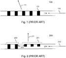
- Fig. 1 illustrates a traditional diffractive coupling grating device 100 as known from the prior art
- Fig. 2 illustrates a diffractive coupling grating device 200 with second order coupling grating, phase delay section and reflector grating as known from the closest prior art
- Fig. 3 illustrates a first embodiment 300 of the diffractive coupling grating device according to the invention
- Fig. 4A and Fig. 4B are top views of respectively the first embodiment 300 and a second embodiment 400 of the diffractive coupling grating device according to the invention.
- Fig. 5 shows a graph 500 illustrating the simulated efficiency of an embodiment of the diffractive coupling grating according to the present invention.
- Fig. 1 shows a traditional diffractive coupling grating 100 consisting of etch through fingers 101 in a waveguide layer 104 that is typically integrated in a multilayer photonic device.
- Incident light 110, travelling through the waveguide layer 104 is out-of-plane coupled by the diffractive coupling grating.
- the efficiency cannot be higher than 50 % in the case of perfect perpendicular coupling.
- the outgoing light 111 does not travel in a direction that forms an angle of 90 degrees with the propagation direction of the light 110 in the planar waveguide 104.
- Fig. 2 shows a diffractive coupling grating 200 that couples light 210 travelling through an integrated planar waveguide 204 out-of-plane to travel in a direction 211 perpendicular to the planar waveguide.
- the diffractive coupling grating 200 consists of a second order coupling grating 201, a phase delay section 202 and a reflector grating 203.
- the tolerances on the length of the phase delay section are tight, requiring the second order coupling grating 201 and the reflector grating 203 to be manufactured using a single mask.
- the second order coupling grating 201 requires a shallow etch to avoid back reflections when the material of the waveguide core 204 is silicon with an effective refractive index of 3.48.
- both the second order coupling grating 201 and the reflector grating 203 must be manufactured through a single shallow etch step.
- Such shallow etch step poses difficulties in controlling the etch depth, a parameter that will determine efficiency and direction of the out-of-plane coupling.
- a diffractive coupling grating as shown in Fig. 2 in other words cannot be mass-manufactured reliably for highly efficient perpendicular coupling.
- Fig. 3 shows an embodiment of the diffractive coupling grating 300 according to the present invention.
- the diffractive coupling grating 300 consists of a second order coupling grating 301, a phase delay section 302 and a reflector grating 303, all manufactured in a planar waveguide integrated in a layer 327 of silicon nitride material, 304 or SiN, with effective refractive index between 1.8 and 2.4. Thanks to the material 304 with reduced effective refractive index, the second order coupling grating 301 can be realized with fingers that are etched all the way through the waveguide core layer 327.
- the second order coupling grating 301 and the reflector grating 303 are realized using a single mask.
- the parameters that determine the perpendicular direction of the out-of-plane coupling and the efficiency of the coupling i.e. the grating pitch ⁇ 1 of the second order coupling grating 301, the length ⁇ 2 of the phase delay section 302 and the pitch ⁇ 3 of the reflector grating 303 can be controlled sufficiently accurately to yield a highly efficient, perfectly perpendicular coupling.
- the etch depth of the fingers constituting the second order coupling grating 301 is eliminated as a parameter since a single etch-through process can be used. Thanks to the material with reduced effective refractive index, back reflections are avoided.
- Fig. 3 shows the light 311 travelling through an uppercladding silicon oxide (SiO 2 ) layer 328 in a direction perfectly perpendicular to the propagation direction 310 of light in the waveguide core layer 327.
- Fig. 3 further shows a number of undercladding layers, alternatingly made out of silicon Si and silicon oxide Si02. These undercladding layers, 321, 322, 323, 324, 325 and 326, form a distributed Bragg reflector, mirroring the light to minimize losses in a substrate and further increase the efficiency of the coupling device 300.
- any other waveguide material with effective refractive index between 1.8 and 2.4 could be used to realize variant embodiments for the one shown in Fig. 3 .
- One example of such material is an engineered material made from silicon whose effective refractive index around 3.48 is reduced to less than 2.4 by using sub-wavelength periodic structures as described in literature already cited here above.
- Fig. 4B shows a top view of an embodiment 400 of the device according to the present invention wherein the waveguide core layer material is engineered from silicon or Si with sub-wavelength holes filled with silicon dioxide or Si02.
- the refractive index of silicon is 3.48 whereas the refractive index of silicon dioxide is 1.45.
- Fig. 4A shows a top view of the above described first embodiment 300 with silicon nitride or SiN as material for the waveguide core layer and silicon dioxide or SiO2 filling the etched fingers as an upper cladding layer on the waveguide.
- Fig. 5 shows the simulated coupling losses 500 for a perfectly perpendicular diffractive coupling grating according to the present invention.
- the diffractive coupling grating is designed for a specific wavelength and it has a certain bandwidth with acceptably high coupling before the efficiency drops dramatically.
- the grating is designed for 1500 nm wavelength, and the thickness of the nitride layer 327 is 400 nm.
- the parameters ⁇ 1, ⁇ 2 and ⁇ 3 are 950 nm, 830 nm and 470 nm respectively.
- the second order coupling grating 301 has 7 periods and reflector grating 303 has 16 periods. As can be seen from Fig.
- losses of less than 3 dB are achieved in the simulation for wavelengths between 1.47 and 1.53 micron and a 6 micron beam diameter.
- This beam diameter is a typical value for a commercially available single-mode VCSEL emitting light with a wavelength of 1500 nm. Since a 3 dB loss corresponds with an efficiency of 50 %, the diffractive coupling grating according to the present invention enables to achieve perfect perpendicular coupling with an efficiency above 50% within the bandwidth where it is designed for.
- top, bottom, over, under, and the like are introduced for descriptive purposes and not necessarily to denote relative positions. It is to be understood that the terms so used are interchangeable under appropriate circumstances and embodiments of the invention are capable of operating according to the present invention in other sequences, or in orientations different from the one(s) described or illustrated above.
Landscapes
- Physics & Mathematics (AREA)
- General Physics & Mathematics (AREA)
- Optics & Photonics (AREA)
- Optical Integrated Circuits (AREA)
Abstract
Description
- The present invention generally relates to out-of-plane coupling of light between an integrated waveguide, i.e. a waveguide that forms a layer in an integrated photonic circuit, and an optical source or optical receiver. The optical source can for instance be a Vertical-Cavity Surface-Emitting Laser or VCSEL. The optical receiver can for instance be an optical fibre wherein the light must be coupled. The invention in particular concerns perpendicular out-of-plane coupling with reduced coupling loss, i.e. coupling the light in or out of the waveguide under an angle of 90 degrees with increased efficiency.
- The article "An Out-of-Plane Grating Coupler for Efficient Butt-Coupling Between Compact Planar Waveguides and Single-Mode Fibers", from the authors D. Taillaert, W. Bogaerts, P. Bientsman, T. F. Kraus, P. Van Daele, I. Moerman, S. Verstuyft, K. De Mesel, R. Baets, published in the IEEE Journal of Quantum Electronics, Vol. 38, No. 7, July 2002, pages 949-955, describes the best known solution for perpendicular out-of-plane coupling between an integrated waveguide and an optical fibre. The solution consists of a second order coupling grating, a phase delay section, and a reflector grating. The structure is illustrated in Fig. 8a) of the IEEE article from D. Taillaert et al. and may eventually be combined with a multilayer reflector underneath as shown in Fig. 8 b).
- In the known solution from D. Taillaert et al., the second order coupling grating requires a shallow etch to make it sufficiently weak to avoid reflections. Further, the tolerance on the distance between the second order coupling grating and the reflector grating, i.e. the tolerance on the length of the phase delay section, is extremely tight. Therefore, the second order coupling grating and the reflector grating must be etched using a single mask. Unfortunately, this implies that also the reflector grating must be made using a shallow etch. Further, it turns out that the phase delay is dependent on the depth of the shallow etch. The etch control of a shallow etch however is too poor to meet the required tolerance in the phase delay.
- Attempts to manufacture a perpendicular coupling grating with second order grating, phase delay section and reflector grating wherein the reflector grating is made in a different etch step using an etch step completely through the waveguide layer instead of a shallow etch, fails as the alignment tolerance from one layer to another is insufficient to meet the distance tolerance requirement.
- The article "Characterization of Silicon-on-Insulator Waveguide Chirped Grating for Coupling to a Vertical Optical Fiber" from the authors X. Chen, C. Li and H. K. Tsang, published in 2008 IEEE/LEOS International Conference on Optical Mems and Nanophotonics, pages 56-57, describes a perfectly perpendicular grating coupler based on a linearly chirped waveguide grating that suppresses back reflections in the waveguide, and consequently improves coupling into an optical fibre. The linearly chirped grating requires a shallow etch (see
paragraph 2, 6th line) suffering tolerance related disadvantages similar to the solution known from D. Taillaert et al. The article further mentions on page 57 that only a maximum coupling efficiency around 32 % is achievable. - United States Patent Application
US 2002/0192849 entitled "Low Diode Feedback" mentions vertical coupling but in fact discloses a device that couples light out of an integrated waveguide under an angle substantially different from 90 degrees, even up to 45 degrees (see for instanceUS 2002/0192849 , page 1, rightmost column, lines 5-8). The out-of-plane coupling inUS 2002/0192849 is realized through a first order shaped grating with fingers having varying lengths or varying depths. As is illustrated byFig. 4 ,Fig. 5 , Fig. 6, Fig. 7, Fig. 8 and Fig. 9, a shallow etch is required to realize such grating, hence suffering from disadvantages that are similar to the ones listed for the closest prior art solution known from D. Taillaert et al. - International Patent Application
WO 2004/051327 entitled "Optical Via For Three Dimensional Interconnection" describes perpendicular coupling of light coming from a VCSEL into an integrated waveguide with improved coupling efficiency. Although the coupling is perpendicular, i.e. realizing an angle of 90 degrees, the device does not use a diffraction grating but a redirection device or mirror, and a taper. This technology is completely different from a diffraction grating, using a much larger, probably polymer structure. - It is an objective of the present invention to disclose a diffractive coupling grating device for perpendicular out-of-plane coupling of light based on a second order coupling grating, phase delay section, and reflector grating, but which overcomes the above mentioned disadvantages of the best existing solution. In particular, it is an objective to realize such diffractive coupling grating device thereby avoiding difficulties and inefficiencies resulting from a poor etch depth control and/or a poor control on the length of the phase delay section. It is a further objective to realize such a diffractive coupling grating device with improved coupling efficiency, i.e. achieving a coupling efficiency above 50 %.
- According to the present invention, the above defined objectives are realized by a diffractive coupling grating as defined by claim 1, for perpendicular, out-of-plane coupling of light between an integrated waveguide and an optical receiver/optical transmitter, the integrated waveguide having a first direction and the light having between the integrated waveguide and the optical receiver/optical transmitter a second direction substantially perpendicular to the first direction, the diffractive coupling grating comprising a second order coupling grating, a phase delay section and a reflector grating, wherein:
- the diffractive coupling grating is manufactured in a layer of material with effective refractive index in a range between 1.8 and 2.4; and
- the second order coupling grating and the reflector grating consist of etch-through fingers manufactured using a single mask.
- Thus, the invention relies on the insight that when the effective refractive index of the material in the waveguide core layer is reduced to a value in the range from 1.8 to 2.4, it becomes possible to devise a process wherein the second order grating fingers can be etched all the way through the waveguide core layer. This way, etch depth is eliminated as a process variable, and evidently also the difficulties in controlling the etch depth. After etching, a material with a lower refractive index is deposited, e.g. silicon oxide or SiO2 with a refractive index of 1.45, that fills the etched fingers and forms an upper cladding layer on the waveguide. As a consequence, the second order coupling grating and the reflector grating can be realized using a single mask, which further eliminates the difficulties in controlling the distance between the second order grating and the reflector grating, i.e. the length of the phase delay section.
- In a first preferred embodiment of the diffractive coupling grating according to the present invention, defined by
claim 2, silicon nitride is used as material with reduced effective refractive index. - Indeed, one way to reduce the effective refractive index of the material to eliminate the need for a shallow etch process consists in using Si3N4 or silicon nitride as material for the waveguide core layer.
- In a second preferred embodiment of the diffractive coupling grating according to the present invention, defined by claim 3, the material with reduced effective refractive index is silicon whose effective refractive index has been reduced below 2.4 through a sub-wavelength periodic structure technique.
- Thus, an alternative way for reducing the effective refractive index of the material consists in using sub-wavelength periodic structures. Using this technique, the effective refractive index of silicon can be reduced from around 3.48 to less than 2.4. The technique is described in more detail in the article "Subwavelength Grating Periodic Structures in Silicon-on-Insulator: a New Type of Microphotonic Waveguide" from the authors Przemek J. Bock, Pavel Cheben, Jens H. Schmid, Jean Lapointe, André Delâge, Siegfried Janz, Geof C. aers, Dan-Xia Xu, Adam Densmore and Trevor J. Hall. This article was published on 13 September 2010 in Optics Express, Vol. 18, No. 19.
- It is noticed that the effective refractive index of the material used for the waveguide core layer should not be confused with the effective index of a waveguide mode, which is also dependent on the core layer thickness and the refractive index of the cladding layers. In case of a plain material without sub-wavelength structures, the effective refractive index corresponds to the refractive index of the material itself. In case of an engineered material like for instance silicon, whose refractive index is 3.48, with sub-wavelength holes filled with silicon dioxide, whose refractive index is 1.45, the effective refractive index of the engineered material will be in between the refractive index of silicon and the refractive index of silicon dioxide.
-
Fig. 1 illustrates a traditional diffractivecoupling grating device 100 as known from the prior art; -
Fig. 2 illustrates a diffractivecoupling grating device 200 with second order coupling grating, phase delay section and reflector grating as known from the closest prior art; -
Fig. 3 illustrates afirst embodiment 300 of the diffractive coupling grating device according to the invention; -
Fig. 4A and Fig. 4B are top views of respectively thefirst embodiment 300 and asecond embodiment 400 of the diffractive coupling grating device according to the invention; and -
Fig. 5 shows agraph 500 illustrating the simulated efficiency of an embodiment of the diffractive coupling grating according to the present invention. -
Fig. 1 shows a traditionaldiffractive coupling grating 100 consisting of etch throughfingers 101 in awaveguide layer 104 that is typically integrated in a multilayer photonic device.Incident light 110, travelling through thewaveguide layer 104 is out-of-plane coupled by the diffractive coupling grating. With such traditional diffractive coupling grating 100 it is not possible to realize a perfect perpendicular out-of-plane coupling with high efficiency. Because of symmetry reasons, the efficiency cannot be higher than 50 % in the case of perfect perpendicular coupling. In other words, theoutgoing light 111 does not travel in a direction that forms an angle of 90 degrees with the propagation direction of thelight 110 in theplanar waveguide 104. In many applications however, e.g. the coupling of light between a VCSEL and an integrated waveguide, or the coupling of light between an integrated waveguide and an optical fibre positioned perpendicular to the planar waveguide, a perfect perpendicular coupling with high efficiency is desired. -
Fig. 2 shows a diffractive coupling grating 200 that couples light 210 travelling through an integratedplanar waveguide 204 out-of-plane to travel in adirection 211 perpendicular to the planar waveguide. The diffractive coupling grating 200 consists of a second order coupling grating 201, aphase delay section 202 and areflector grating 203. As explained already above, the tolerances on the length of the phase delay section are tight, requiring the second order coupling grating 201 and the reflector grating 203 to be manufactured using a single mask. The second order coupling grating 201 requires a shallow etch to avoid back reflections when the material of thewaveguide core 204 is silicon with an effective refractive index of 3.48. As a consequence, both the second order coupling grating 201 and the reflector grating 203 must be manufactured through a single shallow etch step. Such shallow etch step however poses difficulties in controlling the etch depth, a parameter that will determine efficiency and direction of the out-of-plane coupling. A diffractive coupling grating as shown inFig. 2 in other words cannot be mass-manufactured reliably for highly efficient perpendicular coupling. -
Fig. 3 shows an embodiment of the diffractive coupling grating 300 according to the present invention. Just like the grating drawn inFig. 2 , the diffractive coupling grating 300 consists of a second order coupling grating 301, aphase delay section 302 and a reflector grating 303, all manufactured in a planar waveguide integrated in alayer 327 of silicon nitride material, 304 or SiN, with effective refractive index between 1.8 and 2.4. Thanks to thematerial 304 with reduced effective refractive index, the second order coupling grating 301 can be realized with fingers that are etched all the way through thewaveguide core layer 327. The second order coupling grating 301 and the reflector grating 303 are realized using a single mask. As a consequence, the parameters that determine the perpendicular direction of the out-of-plane coupling and the efficiency of the coupling, i.e. the grating pitch Λ1 of the second order coupling grating 301, the length Λ2 of thephase delay section 302 and the pitch Λ3 of the reflector grating 303 can be controlled sufficiently accurately to yield a highly efficient, perfectly perpendicular coupling. The etch depth of the fingers constituting the second order coupling grating 301 is eliminated as a parameter since a single etch-through process can be used. Thanks to the material with reduced effective refractive index, back reflections are avoided. -
Fig. 3 shows the light 311 travelling through an uppercladding silicon oxide (SiO2)layer 328 in a direction perfectly perpendicular to thepropagation direction 310 of light in thewaveguide core layer 327.Fig. 3 further shows a number of undercladding layers, alternatingly made out of silicon Si and silicon oxide Si02. These undercladding layers, 321, 322, 323, 324, 325 and 326, form a distributed Bragg reflector, mirroring the light to minimize losses in a substrate and further increase the efficiency of thecoupling device 300. - It is noticed that as an alternative to silicon nitride SiN, any other waveguide material with effective refractive index between 1.8 and 2.4 could be used to realize variant embodiments for the one shown in
Fig. 3 . One example of such material is an engineered material made from silicon whose effective refractive index around 3.48 is reduced to less than 2.4 by using sub-wavelength periodic structures as described in literature already cited here above.Fig. 4B shows a top view of anembodiment 400 of the device according to the present invention wherein the waveguide core layer material is engineered from silicon or Si with sub-wavelength holes filled with silicon dioxide or Si02. The refractive index of silicon is 3.48 whereas the refractive index of silicon dioxide is 1.45. The material is engineered to have an effective refractive index in the range of 1.8 to 2.4. In comparison,Fig. 4A shows a top view of the above describedfirst embodiment 300 with silicon nitride or SiN as material for the waveguide core layer and silicon dioxide or SiO2 filling the etched fingers as an upper cladding layer on the waveguide. -
Fig. 5 shows thesimulated coupling losses 500 for a perfectly perpendicular diffractive coupling grating according to the present invention. The diffractive coupling grating is designed for a specific wavelength and it has a certain bandwidth with acceptably high coupling before the efficiency drops dramatically. In this specific example, the grating is designed for 1500 nm wavelength, and the thickness of thenitride layer 327 is 400 nm. The parameters Λ1, Λ2 and Λ3 are 950 nm, 830 nm and 470 nm respectively. The second order coupling grating 301 has 7 periods and reflector grating 303 has 16 periods. As can be seen fromFig. 5 , losses of less than 3 dB are achieved in the simulation for wavelengths between 1.47 and 1.53 micron and a 6 micron beam diameter. This beam diameter is a typical value for a commercially available single-mode VCSEL emitting light with a wavelength of 1500 nm. Since a 3 dB loss corresponds with an efficiency of 50 %, the diffractive coupling grating according to the present invention enables to achieve perfect perpendicular coupling with an efficiency above 50% within the bandwidth where it is designed for. - Although the present invention has been illustrated by reference to specific embodiments, it will be apparent to those skilled in the art that the invention is not limited to the details of the foregoing illustrative embodiments, and that the present invention may be embodied with various changes and modifications without departing from the scope thereof. The present embodiments are therefore to be considered in all respects as illustrative and not restrictive, the scope of the invention being indicated by the appended claims rather than by the foregoing description, and all changes which come within the meaning and range of equivalency of the claims are therefore intended to be embraced therein. In other words, it is contemplated to cover any and all modifications, variations or equivalents that fall within the scope of the basic underlying principles and whose essential attributes are claimed in this patent application. It will furthermore be understood by the reader of this patent application that the words "comprising" or "comprise" do not exclude other elements or steps, that the words "a" or "an" do not exclude a plurality, and that a single element, such as a computer system, a processor, or another integrated unit may fulfil the functions of several means recited in the claims. Any reference signs in the claims shall not be construed as limiting the respective claims concerned. The terms "first", "second", third", "a", "b", "c", and the like, when used in the description or in the claims are introduced to distinguish between similar elements or steps and are not necessarily describing a sequential or chronological order. Similarly, the terms "top", "bottom", "over", "under", and the like are introduced for descriptive purposes and not necessarily to denote relative positions. It is to be understood that the terms so used are interchangeable under appropriate circumstances and embodiments of the invention are capable of operating according to the present invention in other sequences, or in orientations different from the one(s) described or illustrated above.
Claims (3)
- A diffractive coupling grating (300) for perpendicular, out-of-plane coupling of light between an integrated waveguide and an optical receiver/optical transmitter, said integrated waveguide having a first direction (310) and said light having between said integrated waveguide and said optical receiver/optical transmitter a second direction (311) substantially perpendicular to said first direction (310), said diffractive coupling grating comprising a second order coupling grating (301), a phase delay section (302) and a reflector grating (303),
CHARACTERISED IN THAT- said diffractive coupling grating is manufactured in a layer of material (304) with effective refractive index in a range between 1.8 and 2.4; and- said second order coupling grating (301) and said reflector grating (303) consist of etch-through fingers manufactured using a single mask. - A diffractive coupling grating according to claim 1,
wherein said material (304) is silicon nitride. - A diffractive coupling grating according to claim 1,
wherein said material (304) is silicon whose effective refractive index has been reduced below 2.4 through a sub-wavelength periodic structure technique.
Priority Applications (1)
| Application Number | Priority Date | Filing Date | Title |
|---|---|---|---|
| EP12157552.6A EP2634605B1 (en) | 2012-02-29 | 2012-02-29 | A diffractive coupling grating for perpendicular coupling |
Applications Claiming Priority (1)
| Application Number | Priority Date | Filing Date | Title |
|---|---|---|---|
| EP12157552.6A EP2634605B1 (en) | 2012-02-29 | 2012-02-29 | A diffractive coupling grating for perpendicular coupling |
Publications (2)
| Publication Number | Publication Date |
|---|---|
| EP2634605A1 true EP2634605A1 (en) | 2013-09-04 |
| EP2634605B1 EP2634605B1 (en) | 2015-10-28 |
Family
ID=45808205
Family Applications (1)
| Application Number | Title | Priority Date | Filing Date |
|---|---|---|---|
| EP12157552.6A Active EP2634605B1 (en) | 2012-02-29 | 2012-02-29 | A diffractive coupling grating for perpendicular coupling |
Country Status (1)
| Country | Link |
|---|---|
| EP (1) | EP2634605B1 (en) |
Cited By (12)
| Publication number | Priority date | Publication date | Assignee | Title |
|---|---|---|---|---|
| EP2866067A1 (en) * | 2013-10-25 | 2015-04-29 | Forelux Inc. | Grating based optical coupler |
| EP2887110A1 (en) * | 2013-12-20 | 2015-06-24 | IMEC vzw | Integrated photonic coupler |
| WO2015105063A1 (en) * | 2014-01-07 | 2015-07-16 | 技術研究組合光電子融合基盤技術研究所 | Grating coupler and production method therefor |
| US9274283B1 (en) | 2014-09-30 | 2016-03-01 | Globalfoundries Inc. | Silicon photonics alignment tolerant vertical grating couplers |
| CN106461865A (en) * | 2014-03-18 | 2017-02-22 | 华为技术有限公司 | Grating coupler and method of making the same |
| US9651718B2 (en) | 2014-01-27 | 2017-05-16 | Forelux Inc. | Photonic apparatus with periodic structures |
| CN110068889A (en) * | 2019-04-29 | 2019-07-30 | 浙江大学 | A kind of super surface duct coupler of silicon substrate artificial micro-structure |
| US10386581B2 (en) | 2013-10-25 | 2019-08-20 | Forelux Inc. | Grating based optical transmitter |
| US10677965B2 (en) | 2014-01-27 | 2020-06-09 | Forelux Inc. | Optical apparatus for non-visible light applications |
| CN111505774A (en) * | 2019-01-30 | 2020-08-07 | 深圳市速腾聚创科技有限公司 | Grating coupler, manufacturing method thereof and optical phased array device |
| US11175453B2 (en) | 2016-08-19 | 2021-11-16 | Imec Vzw | Photonic circuit with integrated light coupler |
| WO2022002578A1 (en) * | 2020-07-02 | 2022-01-06 | Carl Zeiss Ag | Integrated optical circuit with waveguide lens |
Families Citing this family (22)
| Publication number | Priority date | Publication date | Assignee | Title |
|---|---|---|---|---|
| US11726332B2 (en) | 2009-04-27 | 2023-08-15 | Digilens Inc. | Diffractive projection apparatus |
| WO2016020630A2 (en) | 2014-08-08 | 2016-02-11 | Milan Momcilo Popovich | Waveguide laser illuminator incorporating a despeckler |
| CN106125308B (en) | 2012-04-25 | 2019-10-25 | 罗克韦尔柯林斯公司 | Apparatus and method for displaying images |
| US9933684B2 (en) | 2012-11-16 | 2018-04-03 | Rockwell Collins, Inc. | Transparent waveguide display providing upper and lower fields of view having a specific light output aperture configuration |
| US10241330B2 (en) | 2014-09-19 | 2019-03-26 | Digilens, Inc. | Method and apparatus for generating input images for holographic waveguide displays |
| EP3245444B1 (en) | 2015-01-12 | 2021-09-08 | DigiLens Inc. | Environmentally isolated waveguide display |
| US9632226B2 (en) | 2015-02-12 | 2017-04-25 | Digilens Inc. | Waveguide grating device |
| US10690916B2 (en) | 2015-10-05 | 2020-06-23 | Digilens Inc. | Apparatus for providing waveguide displays with two-dimensional pupil expansion |
| EP3548939A4 (en) | 2016-12-02 | 2020-11-25 | DigiLens Inc. | WAVE GUIDE DEVICE WITH UNIFORM OUTPUT LIGHTING |
| WO2018129398A1 (en) | 2017-01-05 | 2018-07-12 | Digilens, Inc. | Wearable heads up displays |
| US10732569B2 (en) | 2018-01-08 | 2020-08-04 | Digilens Inc. | Systems and methods for high-throughput recording of holographic gratings in waveguide cells |
| KR102745805B1 (en) | 2018-01-08 | 2024-12-20 | 디지렌즈 인코포레이티드. | Method for manufacturing optical waveguide |
| EP3710876A4 (en) | 2018-01-08 | 2022-02-09 | DigiLens Inc. | SYSTEMS AND METHODS OF FABRICATING WAVEGUIDE CELLS |
| US20200225471A1 (en) | 2019-01-14 | 2020-07-16 | Digilens Inc. | Holographic Waveguide Display with Light Control Layer |
| US20200247017A1 (en) | 2019-02-05 | 2020-08-06 | Digilens Inc. | Methods for Compensating for Optical Surface Nonuniformity |
| US20220283377A1 (en) | 2019-02-15 | 2022-09-08 | Digilens Inc. | Wide Angle Waveguide Display |
| CN120405821A (en) | 2019-02-15 | 2025-08-01 | 迪吉伦斯公司 | Method and apparatus for providing holographic waveguide displays using integrated gratings |
| US20200386947A1 (en) | 2019-06-07 | 2020-12-10 | Digilens Inc. | Waveguides Incorporating Transmissive and Reflective Gratings and Related Methods of Manufacturing |
| KR102775783B1 (en) | 2019-08-29 | 2025-02-28 | 디지렌즈 인코포레이티드. | Vacuum grid and method for manufacturing the same |
| US12399326B2 (en) | 2021-01-07 | 2025-08-26 | Digilens Inc. | Grating structures for color waveguides |
| US12158612B2 (en) | 2021-03-05 | 2024-12-03 | Digilens Inc. | Evacuated periodic structures and methods of manufacturing |
| CN118661138A (en) | 2021-12-29 | 2024-09-17 | 迪吉伦斯公司 | Method and system for holographic recording using an inverted master |
Citations (3)
| Publication number | Priority date | Publication date | Assignee | Title |
|---|---|---|---|---|
| US20020192849A1 (en) | 2001-03-22 | 2002-12-19 | Bullington Jeff A. | Low diode feedback |
| WO2004051327A2 (en) | 2002-11-27 | 2004-06-17 | General Electric Company | Optical via for three dimensional interconnection |
| EP1855131A1 (en) * | 2006-05-12 | 2007-11-14 | Interuniversitair Microelektronica Centrum Vzw | Slanted segmented grating coupler |
-
2012
- 2012-02-29 EP EP12157552.6A patent/EP2634605B1/en active Active
Patent Citations (3)
| Publication number | Priority date | Publication date | Assignee | Title |
|---|---|---|---|---|
| US20020192849A1 (en) | 2001-03-22 | 2002-12-19 | Bullington Jeff A. | Low diode feedback |
| WO2004051327A2 (en) | 2002-11-27 | 2004-06-17 | General Electric Company | Optical via for three dimensional interconnection |
| EP1855131A1 (en) * | 2006-05-12 | 2007-11-14 | Interuniversitair Microelektronica Centrum Vzw | Slanted segmented grating coupler |
Non-Patent Citations (6)
| Title |
|---|
| D. TAILLAERT, W. BOGAERTS; P. BIENTSMAN; T. F. KRAUS; P. VAN DAELE; MOERMAN, S. VERSTUYFT; K. DE MESEL; R. BAETS: "An Out-of-Plane Grating Coupler for Efficient Butt-Coupling Between Compact Planar Waveguides and Single-Mode Fibers", IEEE JOURNAL OF QUANTUM ELECTRONICS, vol. 38, no. 7, July 2002 (2002-07-01), pages 949 - 955 |
| HALIR R ET AL: "Single etch fibre-to-chip grating couplers for high-volume production in SOI", INFORMATION PHOTONICS (IP), 2011 ICO INTERNATIONAL CONFERENCE ON, IEEE, 18 May 2011 (2011-05-18), pages 1 - 2, XP031892939, ISBN: 978-1-61284-315-5, DOI: 10.1109/ICO-IP.2011.5953786 * |
| PRZEMEK J. BOCK; PAVEL CHEBEN; JENS H. SCHMID; JEAN LAPOINTE, ANDRE DE ÀGE; SIEGFRIED JANZ; GEOF C. AERS; DAN-XIA XU; ADAM DENSMO: "Subwavelength Grating Periodic Structures in Silicon-on-Insulator: a New Type of Microphotonic Waveguide", OPTICS EXPRESS, vol. 18, no. 19, 13 September 2010 (2010-09-13) |
| TAILLAERT D ET AL: "AN OUT-OF-PLANE GRATING COUPLER FOR EFFICIENT BUTT-COUPLING BETWEEN COMPACT PLANAR WAVEGUIDES AND SINGLE-MODE FIBERS", IEEE JOURNAL OF QUANTUM ELECTRONICS, IEEE SERVICE CENTER, PISCATAWAY, NJ, USA, vol. 38, no. 7, 1 July 2002 (2002-07-01), pages 949 - 955, XP001169039, ISSN: 0018-9197, DOI: 10.1109/JQE.2002.1017613 * |
| X. CHEN; C. LI; H. K. TSANG: "Characterization of Silicon-on-Insulator Waveguide Chirped Grating for Coupling to a Vertical Optical Fiber", IEEE/LEOS INTERNATIONAL CONFERENCE ON OPTICAL MEMS AND NANOPHOTONICS, 2008, pages 56 - 57 |
| XIA CHEN ET AL: "Nanoholes Grating Couplers for Coupling Between Silicon-on-Insulator Waveguides and Optical Fibers", IEEE PHOTONICS JOURNAL, IEEE, USA, vol. 1, no. 3, 1 September 2009 (2009-09-01), pages 184 - 190, XP011328068, ISSN: 1943-0655, DOI: 10.1109/JPHOT.2009.2031685 * |
Cited By (19)
| Publication number | Priority date | Publication date | Assignee | Title |
|---|---|---|---|---|
| US9239507B2 (en) | 2013-10-25 | 2016-01-19 | Forelux Inc. | Grating based optical coupler |
| US10386581B2 (en) | 2013-10-25 | 2019-08-20 | Forelux Inc. | Grating based optical transmitter |
| US9703043B2 (en) | 2013-10-25 | 2017-07-11 | Forelux Inc. | Grating based optical coupler |
| EP2866067A1 (en) * | 2013-10-25 | 2015-04-29 | Forelux Inc. | Grating based optical coupler |
| US9632248B2 (en) | 2013-12-20 | 2017-04-25 | Imec Vzw | Integrated photonic coupler |
| JP2015121787A (en) * | 2013-12-20 | 2015-07-02 | アイメック・ヴェーゼットウェーImec Vzw | Integrated photonic coupler |
| EP2887110A1 (en) * | 2013-12-20 | 2015-06-24 | IMEC vzw | Integrated photonic coupler |
| WO2015105063A1 (en) * | 2014-01-07 | 2015-07-16 | 技術研究組合光電子融合基盤技術研究所 | Grating coupler and production method therefor |
| JPWO2015105063A1 (en) * | 2014-01-07 | 2017-03-23 | 技術研究組合光電子融合基盤技術研究所 | Grating coupler and manufacturing method thereof |
| US9651718B2 (en) | 2014-01-27 | 2017-05-16 | Forelux Inc. | Photonic apparatus with periodic structures |
| US10539719B2 (en) | 2014-01-27 | 2020-01-21 | Forelux Inc. | Photonic apparatus with periodic structures |
| US10677965B2 (en) | 2014-01-27 | 2020-06-09 | Forelux Inc. | Optical apparatus for non-visible light applications |
| JP2017513056A (en) * | 2014-03-18 | 2017-05-25 | 華為技術有限公司Huawei Technologies Co.,Ltd. | Grating coupler and manufacturing method thereof |
| CN106461865A (en) * | 2014-03-18 | 2017-02-22 | 华为技术有限公司 | Grating coupler and method of making the same |
| US9274283B1 (en) | 2014-09-30 | 2016-03-01 | Globalfoundries Inc. | Silicon photonics alignment tolerant vertical grating couplers |
| US11175453B2 (en) | 2016-08-19 | 2021-11-16 | Imec Vzw | Photonic circuit with integrated light coupler |
| CN111505774A (en) * | 2019-01-30 | 2020-08-07 | 深圳市速腾聚创科技有限公司 | Grating coupler, manufacturing method thereof and optical phased array device |
| CN110068889A (en) * | 2019-04-29 | 2019-07-30 | 浙江大学 | A kind of super surface duct coupler of silicon substrate artificial micro-structure |
| WO2022002578A1 (en) * | 2020-07-02 | 2022-01-06 | Carl Zeiss Ag | Integrated optical circuit with waveguide lens |
Also Published As
| Publication number | Publication date |
|---|---|
| EP2634605B1 (en) | 2015-10-28 |
Similar Documents
| Publication | Publication Date | Title |
|---|---|---|
| EP2634605B1 (en) | A diffractive coupling grating for perpendicular coupling | |
| Son et al. | High-efficiency broadband light coupling between optical fibers and photonic integrated circuits | |
| US10663663B2 (en) | Spot-size converter for optical mode conversion and coupling between two waveguides | |
| CA2734614C (en) | Optical mode transformer, in particular for coupling an optical fiber and a high-index contrast waveguide | |
| US10371895B2 (en) | Spot-size converter for optical mode conversion and coupling between two waveguides | |
| US7184643B2 (en) | Multiple-core planar optical waveguides and methods of fabrication and use thereof | |
| US9453962B2 (en) | Beam combiner | |
| JP6518434B2 (en) | Integrated photonic coupler | |
| US8483528B2 (en) | Optical mode transformer, in particular for coupling an optical fiber and a high-index contrast waveguide | |
| KR101121459B1 (en) | Method and apparatus for compactly coupling an optical fiber and a planar optical wave guide | |
| US8682120B2 (en) | Polarization-independent grating optical coupler | |
| EP2000836A1 (en) | Method and system for a grating multiplexer with optical waveguide coupling | |
| CN107076928A (en) | Method and relevant device, part and system for coupling the waveguide with different mode field diameter | |
| JP2004133446A (en) | Optical module and manufacturing method | |
| JP2007072433A (en) | Optical integrated device and optical control device | |
| US20130343705A1 (en) | Cladding defined transmission grating | |
| JP7024359B2 (en) | Fiber optic connection structure | |
| WO2004097464A2 (en) | Multiple-core planar optical waveguides and methods of fabrication and use thereof | |
| TW201207455A (en) | Optical grating coupler | |
| TW200532270A (en) | Method and apparatus for tapering an optical waveguide | |
| EP4286904B1 (en) | Multiple-tip edge couplers with segmented waveguide cores | |
| CN115508947B (en) | A silicon-based integrated high-performance polarization beam splitter | |
| CA2578541A1 (en) | Interface device for performing mode transformation in optical waveguides | |
| Lee et al. | Asymmetric waveguides vertical couplers for polarization-independent coupling and polarization-mode splitting | |
| WO2023234111A1 (en) | Optical element and method for producing optical element |
Legal Events
| Date | Code | Title | Description |
|---|---|---|---|
| PUAI | Public reference made under article 153(3) epc to a published international application that has entered the european phase |
Free format text: ORIGINAL CODE: 0009012 |
|
| AK | Designated contracting states |
Kind code of ref document: A1 Designated state(s): AL AT BE BG CH CY CZ DE DK EE ES FI FR GB GR HR HU IE IS IT LI LT LU LV MC MK MT NL NO PL PT RO RS SE SI SK SM TR |
|
| AX | Request for extension of the european patent |
Extension state: BA ME |
|
| 17P | Request for examination filed |
Effective date: 20140210 |
|
| RBV | Designated contracting states (corrected) |
Designated state(s): AL AT BE BG CH CY CZ DE DK EE ES FI FR GB GR HR HU IE IS IT LI LT LU LV MC MK MT NL NO PL PT RO RS SE SI SK SM TR |
|
| 17Q | First examination report despatched |
Effective date: 20140318 |
|
| RAP1 | Party data changed (applicant data changed or rights of an application transferred) |
Owner name: HUAWEI TECHNOLOGIES CO., LTD. |
|
| GRAP | Despatch of communication of intention to grant a patent |
Free format text: ORIGINAL CODE: EPIDOSNIGR1 |
|
| INTG | Intention to grant announced |
Effective date: 20150513 |
|
| GRAS | Grant fee paid |
Free format text: ORIGINAL CODE: EPIDOSNIGR3 |
|
| GRAA | (expected) grant |
Free format text: ORIGINAL CODE: 0009210 |
|
| AK | Designated contracting states |
Kind code of ref document: B1 Designated state(s): AL AT BE BG CH CY CZ DE DK EE ES FI FR GB GR HR HU IE IS IT LI LT LU LV MC MK MT NL NO PL PT RO RS SE SI SK SM TR |
|
| REG | Reference to a national code |
Ref country code: GB Ref legal event code: FG4D |
|
| REG | Reference to a national code |
Ref country code: CH Ref legal event code: EP |
|
| REG | Reference to a national code |
Ref country code: AT Ref legal event code: REF Ref document number: 758236 Country of ref document: AT Kind code of ref document: T Effective date: 20151115 |
|
| REG | Reference to a national code |
Ref country code: IE Ref legal event code: FG4D |
|
| REG | Reference to a national code |
Ref country code: DE Ref legal event code: R096 Ref document number: 602012011917 Country of ref document: DE |
|
| REG | Reference to a national code |
Ref country code: FR Ref legal event code: PLFP Year of fee payment: 5 |
|
| REG | Reference to a national code |
Ref country code: LT Ref legal event code: MG4D |
|
| REG | Reference to a national code |
Ref country code: NL Ref legal event code: MP Effective date: 20151028 |
|
| REG | Reference to a national code |
Ref country code: AT Ref legal event code: MK05 Ref document number: 758236 Country of ref document: AT Kind code of ref document: T Effective date: 20151028 |
|
| PG25 | Lapsed in a contracting state [announced via postgrant information from national office to epo] |
Ref country code: HR Free format text: LAPSE BECAUSE OF FAILURE TO SUBMIT A TRANSLATION OF THE DESCRIPTION OR TO PAY THE FEE WITHIN THE PRESCRIBED TIME-LIMIT Effective date: 20151028 Ref country code: NO Free format text: LAPSE BECAUSE OF FAILURE TO SUBMIT A TRANSLATION OF THE DESCRIPTION OR TO PAY THE FEE WITHIN THE PRESCRIBED TIME-LIMIT Effective date: 20160128 Ref country code: NL Free format text: LAPSE BECAUSE OF FAILURE TO SUBMIT A TRANSLATION OF THE DESCRIPTION OR TO PAY THE FEE WITHIN THE PRESCRIBED TIME-LIMIT Effective date: 20151028 Ref country code: LT Free format text: LAPSE BECAUSE OF FAILURE TO SUBMIT A TRANSLATION OF THE DESCRIPTION OR TO PAY THE FEE WITHIN THE PRESCRIBED TIME-LIMIT Effective date: 20151028 Ref country code: IS Free format text: LAPSE BECAUSE OF FAILURE TO SUBMIT A TRANSLATION OF THE DESCRIPTION OR TO PAY THE FEE WITHIN THE PRESCRIBED TIME-LIMIT Effective date: 20160228 Ref country code: ES Free format text: LAPSE BECAUSE OF FAILURE TO SUBMIT A TRANSLATION OF THE DESCRIPTION OR TO PAY THE FEE WITHIN THE PRESCRIBED TIME-LIMIT Effective date: 20151028 Ref country code: IT Free format text: LAPSE BECAUSE OF FAILURE TO SUBMIT A TRANSLATION OF THE DESCRIPTION OR TO PAY THE FEE WITHIN THE PRESCRIBED TIME-LIMIT Effective date: 20151028 |
|
| PG25 | Lapsed in a contracting state [announced via postgrant information from national office to epo] |
Ref country code: PT Free format text: LAPSE BECAUSE OF FAILURE TO SUBMIT A TRANSLATION OF THE DESCRIPTION OR TO PAY THE FEE WITHIN THE PRESCRIBED TIME-LIMIT Effective date: 20160229 Ref country code: PL Free format text: LAPSE BECAUSE OF FAILURE TO SUBMIT A TRANSLATION OF THE DESCRIPTION OR TO PAY THE FEE WITHIN THE PRESCRIBED TIME-LIMIT Effective date: 20151028 Ref country code: SE Free format text: LAPSE BECAUSE OF FAILURE TO SUBMIT A TRANSLATION OF THE DESCRIPTION OR TO PAY THE FEE WITHIN THE PRESCRIBED TIME-LIMIT Effective date: 20151028 Ref country code: FI Free format text: LAPSE BECAUSE OF FAILURE TO SUBMIT A TRANSLATION OF THE DESCRIPTION OR TO PAY THE FEE WITHIN THE PRESCRIBED TIME-LIMIT Effective date: 20151028 Ref country code: LV Free format text: LAPSE BECAUSE OF FAILURE TO SUBMIT A TRANSLATION OF THE DESCRIPTION OR TO PAY THE FEE WITHIN THE PRESCRIBED TIME-LIMIT Effective date: 20151028 Ref country code: GR Free format text: LAPSE BECAUSE OF FAILURE TO SUBMIT A TRANSLATION OF THE DESCRIPTION OR TO PAY THE FEE WITHIN THE PRESCRIBED TIME-LIMIT Effective date: 20160129 Ref country code: RS Free format text: LAPSE BECAUSE OF FAILURE TO SUBMIT A TRANSLATION OF THE DESCRIPTION OR TO PAY THE FEE WITHIN THE PRESCRIBED TIME-LIMIT Effective date: 20151028 Ref country code: AT Free format text: LAPSE BECAUSE OF FAILURE TO SUBMIT A TRANSLATION OF THE DESCRIPTION OR TO PAY THE FEE WITHIN THE PRESCRIBED TIME-LIMIT Effective date: 20151028 |
|
| PG25 | Lapsed in a contracting state [announced via postgrant information from national office to epo] |
Ref country code: CZ Free format text: LAPSE BECAUSE OF FAILURE TO SUBMIT A TRANSLATION OF THE DESCRIPTION OR TO PAY THE FEE WITHIN THE PRESCRIBED TIME-LIMIT Effective date: 20151028 |
|
| REG | Reference to a national code |
Ref country code: DE Ref legal event code: R097 Ref document number: 602012011917 Country of ref document: DE |
|
| PG25 | Lapsed in a contracting state [announced via postgrant information from national office to epo] |
Ref country code: DK Free format text: LAPSE BECAUSE OF FAILURE TO SUBMIT A TRANSLATION OF THE DESCRIPTION OR TO PAY THE FEE WITHIN THE PRESCRIBED TIME-LIMIT Effective date: 20151028 Ref country code: RO Free format text: LAPSE BECAUSE OF FAILURE TO SUBMIT A TRANSLATION OF THE DESCRIPTION OR TO PAY THE FEE WITHIN THE PRESCRIBED TIME-LIMIT Effective date: 20151028 Ref country code: SK Free format text: LAPSE BECAUSE OF FAILURE TO SUBMIT A TRANSLATION OF THE DESCRIPTION OR TO PAY THE FEE WITHIN THE PRESCRIBED TIME-LIMIT Effective date: 20151028 Ref country code: EE Free format text: LAPSE BECAUSE OF FAILURE TO SUBMIT A TRANSLATION OF THE DESCRIPTION OR TO PAY THE FEE WITHIN THE PRESCRIBED TIME-LIMIT Effective date: 20151028 Ref country code: SM Free format text: LAPSE BECAUSE OF FAILURE TO SUBMIT A TRANSLATION OF THE DESCRIPTION OR TO PAY THE FEE WITHIN THE PRESCRIBED TIME-LIMIT Effective date: 20151028 |
|
| PLBE | No opposition filed within time limit |
Free format text: ORIGINAL CODE: 0009261 |
|
| STAA | Information on the status of an ep patent application or granted ep patent |
Free format text: STATUS: NO OPPOSITION FILED WITHIN TIME LIMIT |
|
| PG25 | Lapsed in a contracting state [announced via postgrant information from national office to epo] |
Ref country code: MC Free format text: LAPSE BECAUSE OF FAILURE TO SUBMIT A TRANSLATION OF THE DESCRIPTION OR TO PAY THE FEE WITHIN THE PRESCRIBED TIME-LIMIT Effective date: 20151028 Ref country code: LU Free format text: LAPSE BECAUSE OF FAILURE TO SUBMIT A TRANSLATION OF THE DESCRIPTION OR TO PAY THE FEE WITHIN THE PRESCRIBED TIME-LIMIT Effective date: 20160229 |
|
| REG | Reference to a national code |
Ref country code: CH Ref legal event code: PL |
|
| 26N | No opposition filed |
Effective date: 20160729 |
|
| PG25 | Lapsed in a contracting state [announced via postgrant information from national office to epo] |
Ref country code: LI Free format text: LAPSE BECAUSE OF NON-PAYMENT OF DUE FEES Effective date: 20160229 Ref country code: CH Free format text: LAPSE BECAUSE OF NON-PAYMENT OF DUE FEES Effective date: 20160229 |
|
| PG25 | Lapsed in a contracting state [announced via postgrant information from national office to epo] |
Ref country code: SI Free format text: LAPSE BECAUSE OF FAILURE TO SUBMIT A TRANSLATION OF THE DESCRIPTION OR TO PAY THE FEE WITHIN THE PRESCRIBED TIME-LIMIT Effective date: 20151028 |
|
| REG | Reference to a national code |
Ref country code: IE Ref legal event code: MM4A |
|
| REG | Reference to a national code |
Ref country code: FR Ref legal event code: PLFP Year of fee payment: 6 |
|
| PG25 | Lapsed in a contracting state [announced via postgrant information from national office to epo] |
Ref country code: IE Free format text: LAPSE BECAUSE OF NON-PAYMENT OF DUE FEES Effective date: 20160229 |
|
| PG25 | Lapsed in a contracting state [announced via postgrant information from national office to epo] |
Ref country code: MT Free format text: LAPSE BECAUSE OF FAILURE TO SUBMIT A TRANSLATION OF THE DESCRIPTION OR TO PAY THE FEE WITHIN THE PRESCRIBED TIME-LIMIT Effective date: 20151028 |
|
| REG | Reference to a national code |
Ref country code: FR Ref legal event code: PLFP Year of fee payment: 7 |
|
| PG25 | Lapsed in a contracting state [announced via postgrant information from national office to epo] |
Ref country code: CY Free format text: LAPSE BECAUSE OF FAILURE TO SUBMIT A TRANSLATION OF THE DESCRIPTION OR TO PAY THE FEE WITHIN THE PRESCRIBED TIME-LIMIT Effective date: 20151028 Ref country code: HU Free format text: LAPSE BECAUSE OF FAILURE TO SUBMIT A TRANSLATION OF THE DESCRIPTION OR TO PAY THE FEE WITHIN THE PRESCRIBED TIME-LIMIT; INVALID AB INITIO Effective date: 20120229 |
|
| PG25 | Lapsed in a contracting state [announced via postgrant information from national office to epo] |
Ref country code: TR Free format text: LAPSE BECAUSE OF FAILURE TO SUBMIT A TRANSLATION OF THE DESCRIPTION OR TO PAY THE FEE WITHIN THE PRESCRIBED TIME-LIMIT Effective date: 20151028 Ref country code: MK Free format text: LAPSE BECAUSE OF FAILURE TO SUBMIT A TRANSLATION OF THE DESCRIPTION OR TO PAY THE FEE WITHIN THE PRESCRIBED TIME-LIMIT Effective date: 20151028 Ref country code: MT Free format text: LAPSE BECAUSE OF FAILURE TO SUBMIT A TRANSLATION OF THE DESCRIPTION OR TO PAY THE FEE WITHIN THE PRESCRIBED TIME-LIMIT Effective date: 20160229 |
|
| PG25 | Lapsed in a contracting state [announced via postgrant information from national office to epo] |
Ref country code: BG Free format text: LAPSE BECAUSE OF FAILURE TO SUBMIT A TRANSLATION OF THE DESCRIPTION OR TO PAY THE FEE WITHIN THE PRESCRIBED TIME-LIMIT Effective date: 20151028 |
|
| PG25 | Lapsed in a contracting state [announced via postgrant information from national office to epo] |
Ref country code: AL Free format text: LAPSE BECAUSE OF FAILURE TO SUBMIT A TRANSLATION OF THE DESCRIPTION OR TO PAY THE FEE WITHIN THE PRESCRIBED TIME-LIMIT Effective date: 20151028 |
|
| PGFP | Annual fee paid to national office [announced via postgrant information from national office to epo] |
Ref country code: FR Payment date: 20251231 Year of fee payment: 15 |
|
| PGFP | Annual fee paid to national office [announced via postgrant information from national office to epo] |
Ref country code: GB Payment date: 20260106 Year of fee payment: 15 |
|
| PGFP | Annual fee paid to national office [announced via postgrant information from national office to epo] |
Ref country code: DE Payment date: 20260102 Year of fee payment: 15 |
|
| PGFP | Annual fee paid to national office [announced via postgrant information from national office to epo] |
Ref country code: BE Payment date: 20260105 Year of fee payment: 15 |