EP2634287A1 - Titanium target for sputtering - Google Patents
Titanium target for sputtering Download PDFInfo
- Publication number
- EP2634287A1 EP2634287A1 EP11836191.4A EP11836191A EP2634287A1 EP 2634287 A1 EP2634287 A1 EP 2634287A1 EP 11836191 A EP11836191 A EP 11836191A EP 2634287 A1 EP2634287 A1 EP 2634287A1
- Authority
- EP
- European Patent Office
- Prior art keywords
- sputtering
- titanium
- target
- titanium target
- plane orientation
- Prior art date
- Legal status (The legal status is an assumption and is not a legal conclusion. Google has not performed a legal analysis and makes no representation as to the accuracy of the status listed.)
- Granted
Links
Images
Classifications
-
- C—CHEMISTRY; METALLURGY
- C23—COATING METALLIC MATERIAL; COATING MATERIAL WITH METALLIC MATERIAL; CHEMICAL SURFACE TREATMENT; DIFFUSION TREATMENT OF METALLIC MATERIAL; COATING BY VACUUM EVAPORATION, BY SPUTTERING, BY ION IMPLANTATION OR BY CHEMICAL VAPOUR DEPOSITION, IN GENERAL; INHIBITING CORROSION OF METALLIC MATERIAL OR INCRUSTATION IN GENERAL
- C23C—COATING METALLIC MATERIAL; COATING MATERIAL WITH METALLIC MATERIAL; SURFACE TREATMENT OF METALLIC MATERIAL BY DIFFUSION INTO THE SURFACE, BY CHEMICAL CONVERSION OR SUBSTITUTION; COATING BY VACUUM EVAPORATION, BY SPUTTERING, BY ION IMPLANTATION OR BY CHEMICAL VAPOUR DEPOSITION, IN GENERAL
- C23C14/00—Coating by vacuum evaporation, by sputtering or by ion implantation of the coating forming material
- C23C14/22—Coating by vacuum evaporation, by sputtering or by ion implantation of the coating forming material characterised by the process of coating
- C23C14/34—Sputtering
- C23C14/3407—Cathode assembly for sputtering apparatus, e.g. Target
-
- C—CHEMISTRY; METALLURGY
- C22—METALLURGY; FERROUS OR NON-FERROUS ALLOYS; TREATMENT OF ALLOYS OR NON-FERROUS METALS
- C22C—ALLOYS
- C22C1/00—Making non-ferrous alloys
- C22C1/02—Making non-ferrous alloys by melting
-
- C—CHEMISTRY; METALLURGY
- C22—METALLURGY; FERROUS OR NON-FERROUS ALLOYS; TREATMENT OF ALLOYS OR NON-FERROUS METALS
- C22C—ALLOYS
- C22C14/00—Alloys based on titanium
-
- C—CHEMISTRY; METALLURGY
- C22—METALLURGY; FERROUS OR NON-FERROUS ALLOYS; TREATMENT OF ALLOYS OR NON-FERROUS METALS
- C22F—CHANGING THE PHYSICAL STRUCTURE OF NON-FERROUS METALS AND NON-FERROUS ALLOYS
- C22F1/00—Changing the physical structure of non-ferrous metals or alloys by heat treatment or by hot or cold working
- C22F1/16—Changing the physical structure of non-ferrous metals or alloys by heat treatment or by hot or cold working of other metals or alloys based thereon
- C22F1/18—High-melting or refractory metals or alloys based thereon
- C22F1/183—High-melting or refractory metals or alloys based thereon of titanium or alloys based thereon
-
- C—CHEMISTRY; METALLURGY
- C23—COATING METALLIC MATERIAL; COATING MATERIAL WITH METALLIC MATERIAL; CHEMICAL SURFACE TREATMENT; DIFFUSION TREATMENT OF METALLIC MATERIAL; COATING BY VACUUM EVAPORATION, BY SPUTTERING, BY ION IMPLANTATION OR BY CHEMICAL VAPOUR DEPOSITION, IN GENERAL; INHIBITING CORROSION OF METALLIC MATERIAL OR INCRUSTATION IN GENERAL
- C23C—COATING METALLIC MATERIAL; COATING MATERIAL WITH METALLIC MATERIAL; SURFACE TREATMENT OF METALLIC MATERIAL BY DIFFUSION INTO THE SURFACE, BY CHEMICAL CONVERSION OR SUBSTITUTION; COATING BY VACUUM EVAPORATION, BY SPUTTERING, BY ION IMPLANTATION OR BY CHEMICAL VAPOUR DEPOSITION, IN GENERAL
- C23C14/00—Coating by vacuum evaporation, by sputtering or by ion implantation of the coating forming material
- C23C14/22—Coating by vacuum evaporation, by sputtering or by ion implantation of the coating forming material characterised by the process of coating
- C23C14/34—Sputtering
- C23C14/3407—Cathode assembly for sputtering apparatus, e.g. Target
- C23C14/3414—Metallurgical or chemical aspects of target preparation, e.g. casting, powder metallurgy
Definitions
- the present invention relates to a high-quality titanium target for sputtering, in which impurities content is reduced, and which can prevent occurrence of cracking and breaking even in high-power sputtering (high-rate sputtering), stabilize sputtering characteristics, and effectively suppress occurrence of particles in formation of a film.
- impurity concentrations are all expressed by mass%.
- Thin films used in, for example, semiconductors tend to be further reduced in thickness and size, the distances between each film are extremely short, and the integration density is increasing. This causes a problem that the material constituting a thin film or impurities contained in the thin film diffuse to the adjacent thin film. Accordingly, the constitutive material balance between a thin film and its adjacent film is collapsed to cause a severe problem to decrease the function that should be essentially possessed by the film.
- the film In the process of producing such a thin film, the film is heated to several hundred degrees (Celsius) in some cases, and the temperature also rises during the use of an electronic instrument in which a semiconductor device is integrated. Such a rise in temperature further increases the diffusion rate of the aforementioned material to cause a severe problem of functional depression in the electronic instrument by the diffusion.
- films of titanium, its alloy, titanium silicide, or titanium nitride can be formed by physical vapor deposition such as sputtering or vacuum vapor deposition. Sputtering, which is most widely used among these methods, will be described below.
- the sputtering is a method of allowing positive ions such as Ar + to physically collide with a target disposed on the cathode to release metal atoms constituting the target by the collision energy.
- a nitride can be formed by sputtering using titanium or its alloy (e.g., a TiAl alloy) as a target in an atmosphere of a gas mixture of argon gas and nitrogen.
- this sputtering film In formation of this sputtering film, if the titanium (including alloys and compounds) target contains impurities, coarse grains floating in a sputtering chamber adhere onto a substrate to cause disconnection or short-circuit of a thin film circuit, and the occurrence of particles, which may cause to form protrusions on the film, increases so that a problem occurs that uniform films cannot be formed.
- a titanium thin film may be used as a pasting layer for preventing occurrence of particles when forming a titanium nitride (Ti-N) film, the titanium thin film is hard and cannot have a sufficient strength of adhesion, resulting in peeling off the inner wall or a component of a film formation apparatus. Thus, the titanium thin film does not achieve the function as a pasting layer and causes occurrence of particles.
- Patent Documents 1 and 2 are cited as prior art documents.
- Patent Document 3 describes a titanium target for sputtering showing an X-ray diffraction intensity ratio of (0002)/(10-11) ⁇ 0.8 and (0002)/(10-10) ⁇ 6 on the sputtered surface and having a recrystallized structure with an average crystal grain size of 20 ⁇ m or less, and proposes a titanium target, with which a film can be easily formed in a narrow and deep contact hole and occurrence of particles can be reduced.
- Patent Document 4 describes a titanium target for sputtering having a Vickers hardness in the range of 110 ⁇ HV ⁇ 130 and a recrystallized structure, and proposes a titanium target, with which sputtered grains are arranged in the same direction, a film can be easily formed in a narrow and deep contact hole, and occurrence of particles can be reduced.
- Patent Document 5 describes a titanium target for sputtering where a titanium target material having a recrystallized structure with a maximum grain size of 20 ⁇ m or less and an average crystal grain size of 10 ⁇ m or less is diffusion-bonded to a backing plate primarily made of aluminum, and proposes a titanium target, with which sputtered grains are arranged in the same direction, a film can be easily formed in a narrow and deep contact hole, and occurrence of particles can be reduced.
- cracking or breaking readily occurs during high-power sputtering, and it is thought that the problems described in each document are not sufficiently solved.
- the present invention provides:
- the present invention also provides:
- the titanium target for sputtering has beneficial effects of: inhibiting occurrence of particles and an abnormal discharge phenomenon by reducing impurities contained in the target; preventing occurrence of cracking or breaking even in high-power sputtering (high-rate sputtering); stabilizing sputtering characteristics; and allowing formation of a high-quality film.
- the titanium target for sputtering according to the present invention has a Shore hardness Hs of 20 or more and a basal plane orientation ratio of 70% or less. If the Shore hardness Hs is less than 20, the strength of the titanium target is insufficient, breaking and cracking occur, in particular, in high-power sputtering (high-rate sputtering), and abnormal discharge and occurrence of particles are induced.
- the Shore hardness Hs is preferably 25 or more, and the present invention can achieve such a Shore hardness.
- the titanium target for sputtering according to the present invention has a basal plane orientation ratio of 70% or less.
- the basal plane is a plane having plane index (002), (103), (104), or (105).
- the basal plane orientation ratio of Ti tends to decrease by the introduction of strain. That is, there is a certain correlation between introduction of strain and orientation to some extent, and the basal plane orientation ratio decreases thereby. This is a preferred phenomenon.
- the heat during sputtering also affects crystalline plane orientation to change it.
- the basal plane orientation ratio is preferably 70% or less, and more preferably 55% or less.
- the present invention provides a titanium target for sputtering wherein the purity of titanium is 99.995 mass% or more, excluding gas components.
- gas components such as oxygen, nitrogen, and hydrogen are contained in higher amounts than those of other impurity elements. Though a less content of these gas components is preferred, an amount of gas components at ordinarily-incorporated level does not become harmful for achieving the object of the present invention.
- the present invention also can provide a titanium target for sputtering, wherein the purity of titanium is 99.995 mass% or more, excluding gas components.
- the outermost surface of a target is heated to about 700°C, and the vicinity of the surface is heated to about 500°C.
- the titanium target of the present invention can prevent breaking and cracking even if it is exposed to high temperature. Breaking and cracking of a target are mainly caused by warping during sputtering or low cycle fatigue fracture resulting from cyclic deformation due to the ON/OFF operation for sputtering power application. Accordingly, a titanium target for sputtering not causing breaking and cracking can be provided by increasing the strength (0.2% proof stress) of the target material.
- the 0.2% proof stress in a tensile test at 500°C be 36 N/mm 2 or more.
- a 0.2% proof stress of 36 N/mm 2 or more in a tensile test at 500°C can be achieved by adding impurity elements of Al, Si, S, Cl, Cr, Fe, Ni, As, Zr, Sn, Sb, B, and La in a total amount of 50 mass ppm or less to the target while the purity of titanium being maintained to 99.995 mass% or more, excluding gas components.
- the heat during sputtering also affects crystalline plane orientation.
- a change in crystalline plane orientation affects the film-forming rate and the film quality and is not preferred.
- the aforementioned crystalline orientation of the present invention is not biased to specific crystalline orientation and can reduce a change in crystalline plane orientation and thereby has an effect of maintaining a constant level of film formation quality.
- a titanium target itself has a high purity, a Shore hardness Hs of 20 or more, a basal plane orientation ratio of 70% or less, a 0.2% proof stress of 330 N/mm 2 or more in a tensile test at room temperature (23°C), and a 0.2% proof stress of 36 N/mm 2 or more in a tensile test at 500°C.
- These numerical ranges show the ranges in which effectiveness of the present invention can be realized. In a range lower than the lower limit, the object of the present invention cannot be achieved, and values outside the limitation impair the characteristics as a high-purity target. The numerical values are therefore regulated within the aforementioned ranges.
- the high-purity titanium can be produced by well-known fused salt electrolysis.
- the atmosphere is desirably an inert atmosphere.
- the initial cathode current density during electrolysis is desirably a low current density of 0.6 A/cm 2 or less.
- the electrolysis temperature is preferably 600 to 800°C.
- the electrodeposited Ti obtained thereby is subject to EB (electron beam) melting and is then solidified by cooling into an ingot, and this is subject to hot forging at 800 to 950°C or hot plastic forming such as hot extrusion to prepare a billet.
- EB electron beam
- Such processing can destroy the ununiform and coarse cast structure of the ingot to achieve uniformity and refinement.
- the billet is cut into preforms each having a volume corresponding to that of a target.
- This preform is provided with high strain by cold forging or cold plastic forming such as cold rolling and is formed into a disk-shaped target material, for example.
- the target material having a processed structure storing high strain is rapidly heated using, for example, a fluidized bed furnace and is subject to heat treatment at 400 to 500°C for a short time.
- a target material having a fine recrystallized structure of 20 ⁇ m or less is obtained thereby.
- the processing is completed by this process step.
- the target material is further subject to cold working (usually, reduction of 10 to 30%), followed by finishing such as polishing to yield a titanium target. That is, the present invention is basically a cold-worked material.
- the above-described process is an example of the method of preparing a titanium target of the present invention, and the method of preparing the titanium target of the present invention is not limited thereto as long as the resulting titanium target has a Shore hardness Hs of 20 or more, a basal plane orientation ratio of 70% or less, a 0.2% proof stress of 330 N/mm 2 or more in a tensile test at room temperature (23°C), and a 0.2% proof stress of 36 N/mm 2 or more in a tensile test at 500°C.
- High-purity titanium having a purity of 99.995 mass% produced based on the aforementioned production process was subject to electron beam melting and was processed into Ti ingots of these three Examples by appropriately applying the production conditions shown in above paragraphs [0023] to [0026].
- the ingots were processed into a target shape.
- Table 1 shows the Shore hardness values measured at any three points on the surface of the each target and the average value thereof.
- Table 2 shows the basal plane orientation ratios measured by XRD.
- the elements that is, Al of 1.6 mass ppm (hereinafter, "mass" is omitted); Si of 0.2 ppm; S of 4.3 ppm; Cl of 0 ppm; Cr of 0.3 ppm; Fe of 0.6 ppm; Ni of 0 ppm; As of 0 ppm; Zr of 0.1 ppm; Sn of 0.1 ppm; Sb of 0 ppm; B of 0 ppm; and La of 0 ppm, were added, in the total amount of 7.2 mass ppm, to high-purity titanium having a purity of 99.995 mass% or more, which was produced based on the production process described above.
- trace impurities-added titanium The resulting high-purity titanium maintaining a purity of 99.995 mass% as a whole (hereinafter, referred to as trace impurities-added titanium) was subject to electron beam melting and then was processed into Ti ingots of these three Examples by appropriately applying the production conditions shown in paragraphs [0023] to [0026].
- the ingots were processed into a target shape.
- Table 1 shows the Shore hardness values measured at any three points on the surface of the each target and the average value thereof.
- Table 2 shows the basal plane orientation ratios measured by XRD.
- Ti ingots having a purity of 99.995 mass% which were produced based on the production conditions shown in the above paragraphs [0023] to [0026], were processed into titanium targets (diameter: 300 mm) of these three Comparative Examples without finally being subject to rolling (material that was finished with heat treatment).
- Table 1 shows the Shore hardness values of the titanium targets measured at any three points on the surface of the each target and the average value thereof.
- Table 2 shows the basal plane orientation ratios measured by XRD.
- Example 1 Cold working rate of 10% after heat treatment; Hs of 28.9; basal plane orientation ratio of 47.3%
- Example 2 Cold working rate of 20% after heat treatment; Hs of 27.0; basal plane orientation ratio of 46.0%
- Example 3 Cold working rate of 30% after heat treatment; Hs of 27.2; basal plane orientation ratio of 51.4%
- Example 4 Trace impurities-added titanium + cold working rate of 10% after heat treatment; Hs of 29.5; basal plane orientation ratio of 55.5%
- Example 5 Trace impurities-added titanium + cold working rate of 20% after heat treatment; Hs of 30.1; basal plane orientation ratio of 60.7%
- Example 6 Trace impurities-added titanium + cold working rate of 30% after heat treatment; Hs of 28.8; basal plane orientation ratio of 53.6%
- Fig. 2 is a graph of the results shown in Table 3.
- particles of 0.2 ⁇ m or more were counted.
- the occurrence of particles was suppressed to be low, and which was maintained to be about the same state. That is, in Examples 1 to 6, occurrence of particles was effectively suppressed.
- Comparative Example 1 No cold working after heat treatment; Hs of 18.0; basal plane orientation ratio of 72.2%.
- Comparative Example 2 Cold working rate of 5% after heat treatment; Hs of 18.9; basal plane orientation ratio of 65.1%.
- Comparative Example 3 Cold working rate of 40% after heat treatment, where processing was incomplete due to severe warping during processing and a target could not be produced therefore.
- the respective tensile test pieces were produced so that the radial direction of a circular target would become the longitudinal direction.
- the test pieces were sampled from three positions, i.e., the center, 1/2R, and the outer periphery, of each of the circular sputtering targets produced in Examples and Comparative Examples, and the average of 0.2% proof stress values at three positions was used as the 0.2% proof stress in each Example or Comparative Example.
- Example 1 cold working rate after heat treatment 10% 352 18
- Example 2 cold working rate after heat treatment 20% 331 16
- Example 4 trace impurities-added titanium + cold working rate after heat treatment: 10% 370 37
- Example 5 trace impurities-added titanium + cold working rate after heat treatment: 20% 382 40
- Example 6 trace impurities-added titanium + cold working rate after heat treatment: 30% 365 38 Comparative Example 1 no cold working after heat treatment 134 18 Comparative Example 2 cold working rate after heat treatment: 5% 165 16 Comparative Example 3 cold working rate after heat treatment: 40% Unable to process
- Example 1 to 6 where appropriate degrees of cold working were performed, the 0.2% proof stress at room temperature was notably increased in comparison to those in Comparative Examples. Furthermore, in Examples 4 to 6 using trace impurities-added titanium, the 0.2% proof stress at room temperature was further increased even in comparison with those in Examples 1 to 3, and the 0.2% proof stress at 500°C has doubled in comparison to those in Comparative Examples 1 and 2 and Examples 1 to 3. Thus, as to these titanium targets, the cracking resistance in high-power sputtering, in which a target is exposed to high temperature, was further improved.
- the present invention is useful for forming thin films for, for example, electronic instruments.
Landscapes
- Chemical & Material Sciences (AREA)
- Engineering & Computer Science (AREA)
- Materials Engineering (AREA)
- Mechanical Engineering (AREA)
- Metallurgy (AREA)
- Organic Chemistry (AREA)
- Chemical Kinetics & Catalysis (AREA)
- Physics & Mathematics (AREA)
- Thermal Sciences (AREA)
- Crystallography & Structural Chemistry (AREA)
- Physical Vapour Deposition (AREA)
- Electrodes Of Semiconductors (AREA)
Abstract
Description
- The present invention relates to a high-quality titanium target for sputtering, in which impurities content is reduced, and which can prevent occurrence of cracking and breaking even in high-power sputtering (high-rate sputtering), stabilize sputtering characteristics, and effectively suppress occurrence of particles in formation of a film. Note that throughout the description, impurity concentrations are all expressed by mass%.
- In recent years, various electronic instruments have been developed originated from a significant progress of semiconductors, and improvements in performance of the instruments and development of novel instruments are being performed daily and hourly.
In such a circumstance, there is a tendency that electronic and device instruments are further reduced in size and are increased in degree of integration. A large number of thin films are formed in various steps of producing these instruments, and titanium is also utilized due to the specific metallic properties thereof in formation of thin films of many electronic instruments as, for example, titanium films or its alloy films, titanium silicide films, or titanium nitride films.
In the case of forming such thin films of titanium (including alloys and compounds of titanium), it should be paid attention that titanium itself is required to have a significantly high purity. - Thin films used in, for example, semiconductors tend to be further reduced in thickness and size, the distances between each film are extremely short, and the integration density is increasing. This causes a problem that the material constituting a thin film or impurities contained in the thin film diffuse to the adjacent thin film. Accordingly, the constitutive material balance between a thin film and its adjacent film is collapsed to cause a severe problem to decrease the function that should be essentially possessed by the film.
- In the process of producing such a thin film, the film is heated to several hundred degrees (Celsius) in some cases, and the temperature also rises during the use of an electronic instrument in which a semiconductor device is integrated. Such a rise in temperature further increases the diffusion rate of the aforementioned material to cause a severe problem of functional depression in the electronic instrument by the diffusion. In general, for example, films of titanium, its alloy, titanium silicide, or titanium nitride can be formed by physical vapor deposition such as sputtering or vacuum vapor deposition. Sputtering, which is most widely used among these methods, will be described below.
- The sputtering is a method of allowing positive ions such as Ar+ to physically collide with a target disposed on the cathode to release metal atoms constituting the target by the collision energy. A nitride can be formed by sputtering using titanium or its alloy (e.g., a TiAl alloy) as a target in an atmosphere of a gas mixture of argon gas and nitrogen.
In formation of this sputtering film, if the titanium (including alloys and compounds) target contains impurities, coarse grains floating in a sputtering chamber adhere onto a substrate to cause disconnection or short-circuit of a thin film circuit, and the occurrence of particles, which may cause to form protrusions on the film, increases so that a problem occurs that uniform films cannot be formed. - Because of this, it is obviously necessary to reduce the amounts of transition metals, high melting metals, alkali metals, alkali earth metals, and other metals, which are conventionally recognized as impurities. Unfortunately, even if these elements are reduced as much as possible, the aforementioned particles occur. Thus, no fundamental solution has been found yet.
In addition, though a titanium thin film may be used as a pasting layer for preventing occurrence of particles when forming a titanium nitride (Ti-N) film, the titanium thin film is hard and cannot have a sufficient strength of adhesion, resulting in peeling off the inner wall or a component of a film formation apparatus. Thus, the titanium thin film does not achieve the function as a pasting layer and causes occurrence of particles. - Furthermore, recently, there is a demand for high-rate sputtering (high-power sputtering) in order to increase the production efficiency. In such sputtering, cracking or breaking of the target tends to occur, and it causes a problem of preventing stable sputtering.
Patent Documents
Patent Document 3 describes a titanium target for sputtering showing an X-ray diffraction intensity ratio of (0002)/(10-11)≧0.8 and (0002)/(10-10)≧6 on the sputtered surface and having a recrystallized structure with an average crystal grain size of 20 µm or less, and proposes a titanium target, with which a film can be easily formed in a narrow and deep contact hole and occurrence of particles can be reduced. -
Patent Document 4 describes a titanium target for sputtering having a Vickers hardness in the range of 110≦HV≦130 and a recrystallized structure, and proposes a titanium target, with which sputtered grains are arranged in the same direction, a film can be easily formed in a narrow and deep contact hole, and occurrence of particles can be reduced. -
Patent Document 5 describes a titanium target for sputtering where a titanium target material having a recrystallized structure with a maximum grain size of 20 µm or less and an average crystal grain size of 10 µm or less is diffusion-bonded to a backing plate primarily made of aluminum, and proposes a titanium target, with which sputtered grains are arranged in the same direction, a film can be easily formed in a narrow and deep contact hole, and occurrence of particles can be reduced.
In the inventions proposed in the aforementioned documents, however, cracking or breaking readily occurs during high-power sputtering, and it is thought that the problems described in each document are not sufficiently solved. -
- Patent Document 1: International Publication No.
WO 01/038598 - Patent Document 2: Published Japanese Translation No.
2001-509548 of PCT - Patent Document 3: Japanese Laid-Open Patent Publication No.
H8-269701 - Patent Document 4: Japanese Laid-Open Patent Publication No.
H9-104972 - Patent Document 5: Japanese Laid-Open Patent Publication No.
H9-143704 - It is an object of the present invention to solve the above-described problems and to provide a high-quality titanium target for sputtering, in which impurities causing occurrence of particles and an abnormal discharge phenomenon are reduced, and which can prevent occurrence of cracking or breaking even in high-power sputtering (high-rate sputtering), stabilize sputtering characteristics, and effectively suppress occurrence of particles during formation of a film.
- The present invention provides:
- 1) a titanium target for sputtering, wherein the Shore hardness Hs is 20 or more and the basal plane orientation ratio is 70% or less.
- The present invention also provides:
- 2) the titanium target for sputtering according to 1) above, wherein the titanium has a purity of 99.995 mass% or more, excluding gas components;
- 3) the titanium target for sputtering according to 1) above, wherein the Shore hardness Hs is 25 or more; and
- 4) the titanium target for sputtering according to any one of 1) to 3) above, wherein the basal plane orientation ratio is 55% or less.
- 5) the titanium target for sputtering according to any one of 1) to 4) above, wherein the 0.2% proof stress in a tensile test at room temperature (23°C) is 330 N/mm2 or more; and
- 6) the titanium target for sputtering according to any one of 1) to 5) above, wherein the 0.2% proof stress in a tensile test at 500°C is 36 N/mm2 or more.
- The titanium target for sputtering has beneficial effects of: inhibiting occurrence of particles and an abnormal discharge phenomenon by reducing impurities contained in the target; preventing occurrence of cracking or breaking even in high-power sputtering (high-rate sputtering); stabilizing sputtering characteristics; and allowing formation of a high-quality film.
-
- [
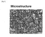
Fig. 1 ] This is an SEM photograph of a sputtered surface of a titanium target for sputtering of the present invention. - [
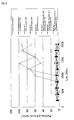
Fig. 2 ] This is a graph showing the observation results of occurrence of particles when sputtering with each target in Examples 1 to 6 and Comparative Examples 1 and 2. - The titanium target for sputtering according to the present invention has a Shore hardness Hs of 20 or more and a basal plane orientation ratio of 70% or less.
If the Shore hardness Hs is less than 20, the strength of the titanium target is insufficient, breaking and cracking occur, in particular, in high-power sputtering (high-rate sputtering), and abnormal discharge and occurrence of particles are induced. The Shore hardness Hs is preferably 25 or more, and the present invention can achieve such a Shore hardness. - In addition, the titanium target for sputtering according to the present invention has a basal plane orientation ratio of 70% or less. The basal plane is a plane having plane index (002), (103), (104), or (105).
- In general, cold working of the sputtering surface of a target induces strain, and the hardness increases. The basal plane orientation ratio of Ti tends to decrease by the introduction of strain. That is, there is a certain correlation between introduction of strain and orientation to some extent, and the basal plane orientation ratio decreases thereby. This is a preferred phenomenon.
As described below, the heat during sputtering also affects crystalline plane orientation to change it. Even in the basal plane of Ti, when the orientation ratio of a specific plane exceeds 70%, the degree of a change caused by the heat during sputtering becomes large to affect the film-forming rate and the film quality. Accordingly, the basal plane orientation ratio is preferably 70% or less, and more preferably 55% or less. - Furthermore, the present invention provides a titanium target for sputtering wherein the purity of titanium is 99.995 mass% or more, excluding gas components. In general, gas components such as oxygen, nitrogen, and hydrogen are contained in higher amounts than those of other impurity elements. Though a less content of these gas components is preferred, an amount of gas components at ordinarily-incorporated level does not become harmful for achieving the object of the present invention. The present invention also can provide a titanium target for sputtering, wherein the purity of titanium is 99.995 mass% or more, excluding gas components.
- In sputtering, the outermost surface of a target is heated to about 700°C, and the vicinity of the surface is heated to about 500°C. The titanium target of the present invention can prevent breaking and cracking even if it is exposed to high temperature. Breaking and cracking of a target are mainly caused by warping during sputtering or low cycle fatigue fracture resulting from cyclic deformation due to the ON/OFF operation for sputtering power application. Accordingly, a titanium target for sputtering not causing breaking and cracking can be provided by increasing the strength (0.2% proof stress) of the target material.
- In particular, in order to prevent breaking and cracking of a target in high-power sputtering in which the target is exposed to high temperature, it is desirable that the 0.2% proof stress in a tensile test at 500°C be 36 N/mm2 or more. A 0.2% proof stress of 36 N/mm2 or more in a tensile test at 500°C can be achieved by adding impurity elements of Al, Si, S, Cl, Cr, Fe, Ni, As, Zr, Sn, Sb, B, and La in a total amount of 50 mass ppm or less to the target while the purity of titanium being maintained to 99.995 mass% or more, excluding gas components.
- In addition, the heat during sputtering also affects crystalline plane orientation. A change in crystalline plane orientation affects the film-forming rate and the film quality and is not preferred. The aforementioned crystalline orientation of the present invention, however, is not biased to specific crystalline orientation and can reduce a change in crystalline plane orientation and thereby has an effect of maintaining a constant level of film formation quality.
- The above-described effects can be achieved under the conditions that a titanium target itself has a high purity, a Shore hardness Hs of 20 or more, a basal plane orientation ratio of 70% or less, a 0.2% proof stress of 330 N/mm2 or more in a tensile test at room temperature (23°C), and a 0.2% proof stress of 36 N/mm2 or more in a tensile test at 500°C. These numerical ranges show the ranges in which effectiveness of the present invention can be realized.
In a range lower than the lower limit, the object of the present invention cannot be achieved, and values outside the limitation impair the characteristics as a high-purity target. The numerical values are therefore regulated within the aforementioned ranges. - The high-purity titanium can be produced by well-known fused salt electrolysis. The atmosphere is desirably an inert atmosphere. The initial cathode current density during electrolysis is desirably a low current density of 0.6 A/cm2 or less. The electrolysis temperature is preferably 600 to 800°C.
The electrodeposited Ti obtained thereby is subject to EB (electron beam) melting and is then solidified by cooling into an ingot, and this is subject to hot forging at 800 to 950°C or hot plastic forming such as hot extrusion to prepare a billet. Such processing can destroy the ununiform and coarse cast structure of the ingot to achieve uniformity and refinement. - The billet is cut into preforms each having a volume corresponding to that of a target. This preform is provided with high strain by cold forging or cold plastic forming such as cold rolling and is formed into a disk-shaped target material, for example.
Furthermore, the target material having a processed structure storing high strain is rapidly heated using, for example, a fluidized bed furnace and is subject to heat treatment at 400 to 500°C for a short time. A target material having a fine recrystallized structure of 20 µm or less is obtained thereby. Conventionally, the processing is completed by this process step. In the present invention, however, the target material is further subject to cold working (usually, reduction of 10 to 30%), followed by finishing such as polishing to yield a titanium target. That is, the present invention is basically a cold-worked material. - The above-described process is an example of the method of preparing a titanium target of the present invention, and the method of preparing the titanium target of the present invention is not limited thereto as long as the resulting titanium target has a Shore hardness Hs of 20 or more, a basal plane orientation ratio of 70% or less, a 0.2% proof stress of 330 N/mm2 or more in a tensile test at room temperature (23°C), and a 0.2% proof stress of 36 N/mm2 or more in a tensile test at 500°C.
- Examples of the present invention will be described below. The following Examples are merely examples, and the present invention is not limited thereto. In other words, the present invention includes all other modes and modifications other than these Examples within the scope of the technical idea of the invention.
- High-purity titanium having a purity of 99.995 mass% produced based on the aforementioned production process was subject to electron beam melting and was processed into Ti ingots of these three Examples by appropriately applying the production conditions shown in above paragraphs [0023] to [0026]. The ingots were processed into a target shape.
Table 1 shows the Shore hardness values measured at any three points on the surface of the each target and the average value thereof. Table 2 shows the basal plane orientation ratios measured by XRD. - The elements: that is, Al of 1.6 mass ppm (hereinafter, "mass" is omitted); Si of 0.2 ppm; S of 4.3 ppm; Cl of 0 ppm; Cr of 0.3 ppm; Fe of 0.6 ppm; Ni of 0 ppm; As of 0 ppm; Zr of 0.1 ppm; Sn of 0.1 ppm; Sb of 0 ppm; B of 0 ppm; and La of 0 ppm, were added, in the total amount of 7.2 mass ppm, to high-purity titanium having a purity of 99.995 mass% or more, which was produced based on the production process described above. The resulting high-purity titanium maintaining a purity of 99.995 mass% as a whole (hereinafter, referred to as trace impurities-added titanium) was subject to electron beam melting and then was processed into Ti ingots of these three Examples by appropriately applying the production conditions shown in paragraphs [0023] to [0026]. The ingots were processed into a target shape.
Table 1 shows the Shore hardness values measured at any three points on the surface of the each target and the average value thereof. Table 2 shows the basal plane orientation ratios measured by XRD. - Ti ingots having a purity of 99.995 mass%, which were produced based on the production conditions shown in the above paragraphs [0023] to [0026], were processed into titanium targets (diameter: 300 mm) of these three Comparative Examples without finally being subject to rolling (material that was finished with heat treatment). Table 1 shows the Shore hardness values of the titanium targets measured at any three points on the surface of the each target and the average value thereof. Table 2 shows the basal plane orientation ratios measured by XRD.
-


-

- Shore hardness values and basal plane orientation ratios of targets in Examples 1 to 6
As shown in Table 1, in Examples 1 to 6, the following average Shore hardness Hs values were obtained respectively. In addition, as shown in Table 2, the following basal plane orientation ratios were obtained.
Example 1: Cold working rate of 10% after heat treatment; Hs of 28.9; basal plane orientation ratio of 47.3%
Example 2: Cold working rate of 20% after heat treatment; Hs of 27.0; basal plane orientation ratio of 46.0%
Example 3: Cold working rate of 30% after heat treatment; Hs of 27.2; basal plane orientation ratio of 51.4%
Example 4: Trace impurities-added titanium + cold working rate of 10% after heat treatment; Hs of 29.5; basal plane orientation ratio of 55.5%
Example 5: Trace impurities-added titanium + cold working rate of 20% after heat treatment; Hs of 30.1; basal plane orientation ratio of 60.7%
Example 6: Trace impurities-added titanium + cold working rate of 30% after heat treatment; Hs of 28.8; basal plane orientation ratio of 53.6% - Each of the targets prepared in Examples 1 to 6 and Comparative Examples 1 to 2 was sputtered with a machine as an actual product, and the occurrence of particles was observed. The numbers of the occurred particles are shown in Table 3.
Fig. 2 is a graph of the results shown in Table 3. Here, particles of 0.2 µm or more were counted.
In Examples 1 to 6, though occurrence of particles slightly increased from the initial stage of sputtering to an integral power consumption of 400 kWh, the occurrence of particles was suppressed to be low, and which was maintained to be about the same state. That is, in Examples 1 to 6, occurrence of particles was effectively suppressed. - (Shore hardness values and basal plane orientation ratios of targets in Comparative Examples 1 to 3)
Comparative Example 1: No cold working after heat treatment; Hs of 18.0; basal plane orientation ratio of 72.2%.
Comparative Example 2: Cold working rate of 5% after heat treatment; Hs of 18.9; basal plane orientation ratio of 65.1%.
Comparative Example 3: Cold working rate of 40% after heat treatment, where processing was incomplete due to severe warping during processing and a target could not be produced therefore. - In Comparative Examples 1 to 2, the occurrence of particles was similarly observed. The results are shown in Table 3 and
Fig. 2 . As mentioned above, since any target could not be produced in Comparative Example 3, Table 3 andFig. 2 do not include the results thereof.
As shown in Table 3 andFig. 2 , though occurrence of particles was suppressed to be relatively low from the initial stage of sputtering to an integral power consumption of 800 kWh, sudden occurrence of particles was observed at several points. Then, the occurrence of particles sharply increased till 2000 kWh, and the sputtering became unstable. -
[Table 3] Life (kWhs) Comparative Example 1 Comparative Example 2 (cold working rate: 5%) Example 1 (cold working rate: 10%) Example 2 (cold working rate: 20%) Example 3 (cold working rate: 30%) Example 4 (Trace impurities-added titanium + cold working rate: 10%) Example 5 (Trace impurities-added titanium + cold working rate: 20%) Example 6 (Trace impurities-added titanium + cold working rate: 30%) 0 200 8 5 3 6 4 3 2 4 400 3 5 8 4 4 1 1 10 600 4 7 2 7 6 10 6 9 800 3 4 5 3 8 2 9 3 1000 59 8 7 5 7 1 7 9 1200 71 78 3 3 6 6 3 9 1400 99 46 11 5 5 1 7 5 1600 62 59 4 6 10 9 7 6 1800 89 95 2 8 5 1 6 10 2000 93 68 7 2 8 2 1 5
The test pieces were sampled from three positions, i.e., the center, 1/2R, and the outer periphery, of each of the circular sputtering targets produced in Examples and Comparative Examples, and the average of 0.2% proof stress values at three positions was used as the 0.2% proof stress in each Example or Comparative Example. -
[Table 4] 0.2% Proof stress Room temperature 500°C N/mm2 N/mm2 Example 1 cold working rate after heat treatment: 10% 352 18 Example 2 cold working rate after heat treatment: 20% 331 16 Example 3 cold working rate after heat treatment: 30% 340 17 Example 4 trace impurities-added titanium + cold working rate after heat treatment: 10% 370 37 Example 5 trace impurities-added titanium + cold working rate after heat treatment: 20% 382 40 Example 6 trace impurities-added titanium + cold working rate after heat treatment: 30% 365 38 Comparative Example 1 no cold working after heat treatment 134 18 Comparative Example 2 cold working rate after heat treatment: 5% 165 16 Comparative Example 3 cold working rate after heat treatment: 40% Unable to process - The conditions of the high-temperature tensile test are as follows:
- Test piece shape: JIS Shape (G 0567II-6)
- Test process: conformity to JIS G 0567
- Test machine: 100 kN high-temperature tensile test machine
- Test conditions: room temperature (23°C) and 500°C
- Gauge length: 30 mm
- Test rate: displacement control at 0.3%/min, and 7.5%/min after proof stress
- Temperature-rising rate: 45°C/min, holding for 15 min
- Temperature measurement: the center of a test piece is fixed to thermocouple
- In Examples 1 to 6 where appropriate degrees of cold working were performed, the 0.2% proof stress at room temperature was notably increased in comparison to those in Comparative Examples. Furthermore, in Examples 4 to 6 using trace impurities-added titanium, the 0.2% proof stress at room temperature was further increased even in comparison with those in Examples 1 to 3, and the 0.2% proof stress at 500°C has doubled in comparison to those in Comparative Examples 1 and 2 and Examples 1 to 3. Thus, as to these titanium targets, the cracking resistance in high-power sputtering, in which a target is exposed to high temperature, was further improved.
- It is possible to provide a high-quality titanium target for sputtering, in which impurities causing occurrence of particles and an abnormal discharge phenomenon are reduced, and which can prevent occurrence of cracking or breaking even in high-power sputtering (high-rate sputtering), stabilize sputtering characteristics, and effectively suppress occurrence of particles during formation of a film. Accordingly, the present invention is useful for forming thin films for, for example, electronic instruments.
Claims (6)
- A titanium target for sputtering, wherein the Shore hardness Hs is 20 or more and the basal plane orientation ratio is 70% or less.
- The titanium target for sputtering according to Claim 1, wherein the titanium has a purity of 99.995 mass% or more, excluding gas components.
- The titanium target for sputtering according to Claim 1, wherein the Shore hardness Hs is 25 or more.
- The titanium target for sputtering according to any one of Claims 1 to 3, wherein the basal plane orientation ratio is 55% or less.
- The titanium target for sputtering according to any one of Claims 1 to 4, wherein the 0.2% proof stress in a tensile test at room temperature (23°C) is 330 N/mm2 or more.
- The titanium target for sputtering according to any one of Claims 1 to 5, wherein the 0.2% proof stress in a tensile test at 500°C is 36 N/mm2 or more.
Applications Claiming Priority (2)
| Application Number | Priority Date | Filing Date | Title |
|---|---|---|---|
| JP2010238586 | 2010-10-25 | ||
| PCT/JP2011/074394 WO2012057057A1 (en) | 2010-10-25 | 2011-10-24 | Titanium target for sputtering |
Publications (3)
| Publication Number | Publication Date |
|---|---|
| EP2634287A1 true EP2634287A1 (en) | 2013-09-04 |
| EP2634287A4 EP2634287A4 (en) | 2014-03-19 |
| EP2634287B1 EP2634287B1 (en) | 2017-11-29 |
Family
ID=45993766
Family Applications (1)
| Application Number | Title | Priority Date | Filing Date |
|---|---|---|---|
| EP11836191.4A Active EP2634287B1 (en) | 2010-10-25 | 2011-10-24 | Titanium target for sputtering |
Country Status (8)
| Country | Link |
|---|---|
| US (1) | US9068258B2 (en) |
| EP (1) | EP2634287B1 (en) |
| JP (1) | JP5571196B2 (en) |
| KR (3) | KR20130076863A (en) |
| CN (1) | CN103180482B (en) |
| SG (1) | SG188956A1 (en) |
| TW (1) | TWI558829B (en) |
| WO (1) | WO2012057057A1 (en) |
Cited By (1)
| Publication number | Priority date | Publication date | Assignee | Title |
|---|---|---|---|---|
| EP2738285A4 (en) * | 2012-01-12 | 2015-01-07 | Jx Nippon Mining & Metals Corp | TARGET FOR TITANIUM CATHODIC SPRAY |
Families Citing this family (6)
| Publication number | Priority date | Publication date | Assignee | Title |
|---|---|---|---|---|
| JP5420609B2 (en) | 2010-08-25 | 2014-02-19 | Jx日鉱日石金属株式会社 | Titanium target for sputtering |
| CN104114303B (en) | 2012-02-14 | 2016-12-21 | 吉坤日矿日石金属株式会社 | High-purity titanium ingot, its manufacture method and titanium sputtering target |
| JP6077102B2 (en) | 2013-03-06 | 2017-02-08 | Jx金属株式会社 | Titanium target for sputtering and manufacturing method thereof |
| US10354846B2 (en) * | 2013-11-06 | 2019-07-16 | Jx Nippon Mining & Metals Corporation | Sputtering target-backing plate assembly |
| CN105154834A (en) * | 2015-09-07 | 2015-12-16 | 云南钛业股份有限公司 | Production method of cylindrical titanium sputtering target material |
| JP7179450B2 (en) | 2017-09-21 | 2022-11-29 | Jx金属株式会社 | Titanium target for sputtering, method for producing same, and method for producing titanium-containing thin film |
Family Cites Families (18)
| Publication number | Priority date | Publication date | Assignee | Title |
|---|---|---|---|---|
| JP2901854B2 (en) * | 1993-09-27 | 1999-06-07 | 株式会社ジャパンエナジー | High purity titanium sputtering target |
| US5772860A (en) | 1993-09-27 | 1998-06-30 | Japan Energy Corporation | High purity titanium sputtering targets |
| JP3413782B2 (en) | 1995-03-31 | 2003-06-09 | 日立金属株式会社 | Titanium target for sputtering and method for producing the same |
| JP2706635B2 (en) | 1995-06-07 | 1998-01-28 | 真空冶金株式会社 | High purity titanium target for sputtering and method for producing the same |
| JPH09104972A (en) * | 1995-10-05 | 1997-04-22 | Hitachi Metals Ltd | Titanium target for sputtering and its production |
| JPH09143704A (en) | 1995-11-27 | 1997-06-03 | Hitachi Metals Ltd | Titanium target for sputtering and its production |
| JP3792291B2 (en) * | 1996-04-01 | 2006-07-05 | 三菱マテリアル株式会社 | Ti target for magnetron sputtering |
| US5993621A (en) | 1997-07-11 | 1999-11-30 | Johnson Matthey Electronics, Inc. | Titanium sputtering target |
| JPH11269621A (en) * | 1997-12-24 | 1999-10-05 | Toho Titanium Co Ltd | Method for working high-purity titanium material |
| KR20020068535A (en) | 1999-11-22 | 2002-08-27 | 가부시키 가이샤 닛코 마테리알즈 | Titanium target for sputtering |
| JP3967515B2 (en) * | 2000-02-16 | 2007-08-29 | 株式会社神戸製鋼所 | Titanium alloy material for muffler and muffler |
| TWI353388B (en) | 2007-09-12 | 2011-12-01 | Taiwan Textile Res Inst | Method for preparing titanium dioxide |
| JP5144576B2 (en) * | 2009-03-31 | 2013-02-13 | Jx日鉱日石金属株式会社 | Titanium target for sputtering |
| JP2011111373A (en) * | 2009-11-27 | 2011-06-09 | Tosoh Corp | Method for producing member with hydrophilized surface |
| CN102791905B (en) | 2010-03-11 | 2015-04-01 | 株式会社东芝 | Sputtering target, manufacturing method thereof, and semiconductor element manufacturing method |
| JP5420609B2 (en) | 2010-08-25 | 2014-02-19 | Jx日鉱日石金属株式会社 | Titanium target for sputtering |
| US8663440B2 (en) | 2010-09-28 | 2014-03-04 | Jx Nippon Mining & Metals Corporation | Titanium target for sputtering |
| SG11201400327SA (en) | 2012-01-12 | 2014-06-27 | Jx Nippon Mining & Metals Corp | Titanium target for sputtering |
-
2011
- 2011-10-24 KR KR1020137006398A patent/KR20130076863A/en not_active Ceased
- 2011-10-24 CN CN201180051337.XA patent/CN103180482B/en active Active
- 2011-10-24 KR KR1020197006865A patent/KR20190027960A/en not_active Ceased
- 2011-10-24 SG SG2013016209A patent/SG188956A1/en unknown
- 2011-10-24 EP EP11836191.4A patent/EP2634287B1/en active Active
- 2011-10-24 WO PCT/JP2011/074394 patent/WO2012057057A1/en not_active Ceased
- 2011-10-24 KR KR1020157027210A patent/KR102080367B1/en active Active
- 2011-10-24 US US13/824,412 patent/US9068258B2/en active Active
- 2011-10-24 JP JP2012540837A patent/JP5571196B2/en active Active
- 2011-10-25 TW TW100138567A patent/TWI558829B/en active
Cited By (1)
| Publication number | Priority date | Publication date | Assignee | Title |
|---|---|---|---|---|
| EP2738285A4 (en) * | 2012-01-12 | 2015-01-07 | Jx Nippon Mining & Metals Corp | TARGET FOR TITANIUM CATHODIC SPRAY |
Also Published As
| Publication number | Publication date |
|---|---|
| US20130186753A1 (en) | 2013-07-25 |
| KR20150114584A (en) | 2015-10-12 |
| SG188956A1 (en) | 2013-05-31 |
| EP2634287A4 (en) | 2014-03-19 |
| KR20190027960A (en) | 2019-03-15 |
| CN103180482B (en) | 2016-05-04 |
| CN103180482A (en) | 2013-06-26 |
| TW201217565A (en) | 2012-05-01 |
| WO2012057057A1 (en) | 2012-05-03 |
| JP5571196B2 (en) | 2014-08-13 |
| EP2634287B1 (en) | 2017-11-29 |
| JPWO2012057057A1 (en) | 2014-05-12 |
| KR20130076863A (en) | 2013-07-08 |
| KR102080367B1 (en) | 2020-02-21 |
| US9068258B2 (en) | 2015-06-30 |
| TWI558829B (en) | 2016-11-21 |
Similar Documents
| Publication | Publication Date | Title |
|---|---|---|
| EP2832895B1 (en) | Silver-based cylindrical target | |
| CN100567559C (en) | Less occurrence of particle contain the Mn copper alloy sputtering target | |
| EP2634287B1 (en) | Titanium target for sputtering | |
| EP2674511B1 (en) | Titanium target for sputtering | |
| WO2014136702A1 (en) | Titanium target for sputtering and manufacturing method thereof | |
| EP2604718B1 (en) | Tantalum sputtering target | |
| CN110129744B (en) | Titanium target for sputtering | |
| JP5144576B2 (en) | Titanium target for sputtering | |
| EP3686313A1 (en) | Titanium sputtering target, production method therefor, and method for producing titanium-containing thin film | |
| US8663440B2 (en) | Titanium target for sputtering | |
| TWI433953B (en) | Sputtering titanium target |
Legal Events
| Date | Code | Title | Description |
|---|---|---|---|
| PUAI | Public reference made under article 153(3) epc to a published international application that has entered the european phase |
Free format text: ORIGINAL CODE: 0009012 |
|
| 17P | Request for examination filed |
Effective date: 20130220 |
|
| AK | Designated contracting states |
Kind code of ref document: A1 Designated state(s): AL AT BE BG CH CY CZ DE DK EE ES FI FR GB GR HR HU IE IS IT LI LT LU LV MC MK MT NL NO PL PT RO RS SE SI SK SM TR |
|
| DAX | Request for extension of the european patent (deleted) | ||
| A4 | Supplementary search report drawn up and despatched |
Effective date: 20140218 |
|
| RIC1 | Information provided on ipc code assigned before grant |
Ipc: C23C 14/34 20060101AFI20140212BHEP Ipc: C22F 1/18 20060101ALI20140212BHEP Ipc: C22C 14/00 20060101ALI20140212BHEP |
|
| 17Q | First examination report despatched |
Effective date: 20151214 |
|
| GRAP | Despatch of communication of intention to grant a patent |
Free format text: ORIGINAL CODE: EPIDOSNIGR1 |
|
| RIC1 | Information provided on ipc code assigned before grant |
Ipc: C22C 14/00 20060101ALI20170607BHEP Ipc: C22F 1/18 20060101ALI20170607BHEP Ipc: C23C 14/34 20060101AFI20170607BHEP Ipc: C22C 1/02 20060101ALI20170607BHEP |
|
| INTG | Intention to grant announced |
Effective date: 20170627 |
|
| RIN1 | Information on inventor provided before grant (corrected) |
Inventor name: MAKINO NOBUHITO Inventor name: FUKUYO HIDEAKI Inventor name: TSUKAMOTO SHIRO |
|
| GRAS | Grant fee paid |
Free format text: ORIGINAL CODE: EPIDOSNIGR3 |
|
| GRAA | (expected) grant |
Free format text: ORIGINAL CODE: 0009210 |
|
| AK | Designated contracting states |
Kind code of ref document: B1 Designated state(s): AL AT BE BG CH CY CZ DE DK EE ES FI FR GB GR HR HU IE IS IT LI LT LU LV MC MK MT NL NO PL PT RO RS SE SI SK SM TR |
|
| REG | Reference to a national code |
Ref country code: CH Ref legal event code: EP |
|
| REG | Reference to a national code |
Ref country code: AT Ref legal event code: REF Ref document number: 950474 Country of ref document: AT Kind code of ref document: T Effective date: 20171215 |
|
| REG | Reference to a national code |
Ref country code: IE Ref legal event code: FG4D |
|
| REG | Reference to a national code |
Ref country code: DE Ref legal event code: R096 Ref document number: 602011043858 Country of ref document: DE |
|
| REG | Reference to a national code |
Ref country code: NL Ref legal event code: MP Effective date: 20171129 |
|
| REG | Reference to a national code |
Ref country code: LT Ref legal event code: MG4D |
|
| REG | Reference to a national code |
Ref country code: AT Ref legal event code: MK05 Ref document number: 950474 Country of ref document: AT Kind code of ref document: T Effective date: 20171129 |
|
| PG25 | Lapsed in a contracting state [announced via postgrant information from national office to epo] |
Ref country code: FI Free format text: LAPSE BECAUSE OF FAILURE TO SUBMIT A TRANSLATION OF THE DESCRIPTION OR TO PAY THE FEE WITHIN THE PRESCRIBED TIME-LIMIT Effective date: 20171129 Ref country code: SE Free format text: LAPSE BECAUSE OF FAILURE TO SUBMIT A TRANSLATION OF THE DESCRIPTION OR TO PAY THE FEE WITHIN THE PRESCRIBED TIME-LIMIT Effective date: 20171129 Ref country code: NO Free format text: LAPSE BECAUSE OF FAILURE TO SUBMIT A TRANSLATION OF THE DESCRIPTION OR TO PAY THE FEE WITHIN THE PRESCRIBED TIME-LIMIT Effective date: 20180228 Ref country code: LT Free format text: LAPSE BECAUSE OF FAILURE TO SUBMIT A TRANSLATION OF THE DESCRIPTION OR TO PAY THE FEE WITHIN THE PRESCRIBED TIME-LIMIT Effective date: 20171129 Ref country code: ES Free format text: LAPSE BECAUSE OF FAILURE TO SUBMIT A TRANSLATION OF THE DESCRIPTION OR TO PAY THE FEE WITHIN THE PRESCRIBED TIME-LIMIT Effective date: 20171129 |
|
| PG25 | Lapsed in a contracting state [announced via postgrant information from national office to epo] |
Ref country code: BG Free format text: LAPSE BECAUSE OF FAILURE TO SUBMIT A TRANSLATION OF THE DESCRIPTION OR TO PAY THE FEE WITHIN THE PRESCRIBED TIME-LIMIT Effective date: 20180228 Ref country code: HR Free format text: LAPSE BECAUSE OF FAILURE TO SUBMIT A TRANSLATION OF THE DESCRIPTION OR TO PAY THE FEE WITHIN THE PRESCRIBED TIME-LIMIT Effective date: 20171129 Ref country code: AT Free format text: LAPSE BECAUSE OF FAILURE TO SUBMIT A TRANSLATION OF THE DESCRIPTION OR TO PAY THE FEE WITHIN THE PRESCRIBED TIME-LIMIT Effective date: 20171129 Ref country code: RS Free format text: LAPSE BECAUSE OF FAILURE TO SUBMIT A TRANSLATION OF THE DESCRIPTION OR TO PAY THE FEE WITHIN THE PRESCRIBED TIME-LIMIT Effective date: 20171129 Ref country code: GR Free format text: LAPSE BECAUSE OF FAILURE TO SUBMIT A TRANSLATION OF THE DESCRIPTION OR TO PAY THE FEE WITHIN THE PRESCRIBED TIME-LIMIT Effective date: 20180301 Ref country code: LV Free format text: LAPSE BECAUSE OF FAILURE TO SUBMIT A TRANSLATION OF THE DESCRIPTION OR TO PAY THE FEE WITHIN THE PRESCRIBED TIME-LIMIT Effective date: 20171129 |
|
| PG25 | Lapsed in a contracting state [announced via postgrant information from national office to epo] |
Ref country code: NL Free format text: LAPSE BECAUSE OF FAILURE TO SUBMIT A TRANSLATION OF THE DESCRIPTION OR TO PAY THE FEE WITHIN THE PRESCRIBED TIME-LIMIT Effective date: 20171129 |
|
| PG25 | Lapsed in a contracting state [announced via postgrant information from national office to epo] |
Ref country code: CZ Free format text: LAPSE BECAUSE OF FAILURE TO SUBMIT A TRANSLATION OF THE DESCRIPTION OR TO PAY THE FEE WITHIN THE PRESCRIBED TIME-LIMIT Effective date: 20171129 Ref country code: SK Free format text: LAPSE BECAUSE OF FAILURE TO SUBMIT A TRANSLATION OF THE DESCRIPTION OR TO PAY THE FEE WITHIN THE PRESCRIBED TIME-LIMIT Effective date: 20171129 Ref country code: CY Free format text: LAPSE BECAUSE OF FAILURE TO SUBMIT A TRANSLATION OF THE DESCRIPTION OR TO PAY THE FEE WITHIN THE PRESCRIBED TIME-LIMIT Effective date: 20171129 Ref country code: EE Free format text: LAPSE BECAUSE OF FAILURE TO SUBMIT A TRANSLATION OF THE DESCRIPTION OR TO PAY THE FEE WITHIN THE PRESCRIBED TIME-LIMIT Effective date: 20171129 Ref country code: DK Free format text: LAPSE BECAUSE OF FAILURE TO SUBMIT A TRANSLATION OF THE DESCRIPTION OR TO PAY THE FEE WITHIN THE PRESCRIBED TIME-LIMIT Effective date: 20171129 |
|
| REG | Reference to a national code |
Ref country code: DE Ref legal event code: R097 Ref document number: 602011043858 Country of ref document: DE |
|
| PG25 | Lapsed in a contracting state [announced via postgrant information from national office to epo] |
Ref country code: PL Free format text: LAPSE BECAUSE OF FAILURE TO SUBMIT A TRANSLATION OF THE DESCRIPTION OR TO PAY THE FEE WITHIN THE PRESCRIBED TIME-LIMIT Effective date: 20171129 Ref country code: RO Free format text: LAPSE BECAUSE OF FAILURE TO SUBMIT A TRANSLATION OF THE DESCRIPTION OR TO PAY THE FEE WITHIN THE PRESCRIBED TIME-LIMIT Effective date: 20171129 Ref country code: IT Free format text: LAPSE BECAUSE OF FAILURE TO SUBMIT A TRANSLATION OF THE DESCRIPTION OR TO PAY THE FEE WITHIN THE PRESCRIBED TIME-LIMIT Effective date: 20171129 Ref country code: SM Free format text: LAPSE BECAUSE OF FAILURE TO SUBMIT A TRANSLATION OF THE DESCRIPTION OR TO PAY THE FEE WITHIN THE PRESCRIBED TIME-LIMIT Effective date: 20171129 |
|
| REG | Reference to a national code |
Ref country code: FR Ref legal event code: PLFP Year of fee payment: 8 |
|
| PLBE | No opposition filed within time limit |
Free format text: ORIGINAL CODE: 0009261 |
|
| STAA | Information on the status of an ep patent application or granted ep patent |
Free format text: STATUS: NO OPPOSITION FILED WITHIN TIME LIMIT |
|
| 26N | No opposition filed |
Effective date: 20180830 |
|
| PG25 | Lapsed in a contracting state [announced via postgrant information from national office to epo] |
Ref country code: SI Free format text: LAPSE BECAUSE OF FAILURE TO SUBMIT A TRANSLATION OF THE DESCRIPTION OR TO PAY THE FEE WITHIN THE PRESCRIBED TIME-LIMIT Effective date: 20171129 |
|
| REG | Reference to a national code |
Ref country code: CH Ref legal event code: PL |
|
| GBPC | Gb: european patent ceased through non-payment of renewal fee |
Effective date: 20181024 |
|
| REG | Reference to a national code |
Ref country code: BE Ref legal event code: MM Effective date: 20181031 |
|
| PG25 | Lapsed in a contracting state [announced via postgrant information from national office to epo] |
Ref country code: MC Free format text: LAPSE BECAUSE OF FAILURE TO SUBMIT A TRANSLATION OF THE DESCRIPTION OR TO PAY THE FEE WITHIN THE PRESCRIBED TIME-LIMIT Effective date: 20171129 Ref country code: LU Free format text: LAPSE BECAUSE OF NON-PAYMENT OF DUE FEES Effective date: 20181024 |
|
| REG | Reference to a national code |
Ref country code: IE Ref legal event code: MM4A |
|
| PG25 | Lapsed in a contracting state [announced via postgrant information from national office to epo] |
Ref country code: BE Free format text: LAPSE BECAUSE OF NON-PAYMENT OF DUE FEES Effective date: 20181031 Ref country code: LI Free format text: LAPSE BECAUSE OF NON-PAYMENT OF DUE FEES Effective date: 20181031 Ref country code: CH Free format text: LAPSE BECAUSE OF NON-PAYMENT OF DUE FEES Effective date: 20181031 |
|
| PG25 | Lapsed in a contracting state [announced via postgrant information from national office to epo] |
Ref country code: IE Free format text: LAPSE BECAUSE OF NON-PAYMENT OF DUE FEES Effective date: 20181024 Ref country code: GB Free format text: LAPSE BECAUSE OF NON-PAYMENT OF DUE FEES Effective date: 20181024 |
|
| PG25 | Lapsed in a contracting state [announced via postgrant information from national office to epo] |
Ref country code: MT Free format text: LAPSE BECAUSE OF NON-PAYMENT OF DUE FEES Effective date: 20181024 |
|
| PG25 | Lapsed in a contracting state [announced via postgrant information from national office to epo] |
Ref country code: TR Free format text: LAPSE BECAUSE OF FAILURE TO SUBMIT A TRANSLATION OF THE DESCRIPTION OR TO PAY THE FEE WITHIN THE PRESCRIBED TIME-LIMIT Effective date: 20171129 |
|
| PG25 | Lapsed in a contracting state [announced via postgrant information from national office to epo] |
Ref country code: PT Free format text: LAPSE BECAUSE OF FAILURE TO SUBMIT A TRANSLATION OF THE DESCRIPTION OR TO PAY THE FEE WITHIN THE PRESCRIBED TIME-LIMIT Effective date: 20171129 |
|
| PG25 | Lapsed in a contracting state [announced via postgrant information from national office to epo] |
Ref country code: MK Free format text: LAPSE BECAUSE OF NON-PAYMENT OF DUE FEES Effective date: 20171129 Ref country code: HU Free format text: LAPSE BECAUSE OF FAILURE TO SUBMIT A TRANSLATION OF THE DESCRIPTION OR TO PAY THE FEE WITHIN THE PRESCRIBED TIME-LIMIT; INVALID AB INITIO Effective date: 20111024 |
|
| PG25 | Lapsed in a contracting state [announced via postgrant information from national office to epo] |
Ref country code: AL Free format text: LAPSE BECAUSE OF FAILURE TO SUBMIT A TRANSLATION OF THE DESCRIPTION OR TO PAY THE FEE WITHIN THE PRESCRIBED TIME-LIMIT Effective date: 20171129 Ref country code: IS Free format text: LAPSE BECAUSE OF FAILURE TO SUBMIT A TRANSLATION OF THE DESCRIPTION OR TO PAY THE FEE WITHIN THE PRESCRIBED TIME-LIMIT Effective date: 20180329 |
|
| P01 | Opt-out of the competence of the unified patent court (upc) registered |
Effective date: 20230517 |
|
| PGFP | Annual fee paid to national office [announced via postgrant information from national office to epo] |
Ref country code: FR Payment date: 20250908 Year of fee payment: 15 |
|
| PGFP | Annual fee paid to national office [announced via postgrant information from national office to epo] |
Ref country code: DE Payment date: 20250902 Year of fee payment: 15 |