EP2632042A1 - Apparatus and method for phase locked loop bandwidth expansion - Google Patents
Apparatus and method for phase locked loop bandwidth expansion Download PDFInfo
- Publication number
- EP2632042A1 EP2632042A1 EP13155847.0A EP13155847A EP2632042A1 EP 2632042 A1 EP2632042 A1 EP 2632042A1 EP 13155847 A EP13155847 A EP 13155847A EP 2632042 A1 EP2632042 A1 EP 2632042A1
- Authority
- EP
- European Patent Office
- Prior art keywords
- function
- compensation
- filter
- locked loop
- phase locked
- Prior art date
- Legal status (The legal status is an assumption and is not a legal conclusion. Google has not performed a legal analysis and makes no representation as to the accuracy of the status listed.)
- Granted
Links
Images



Classifications
-
- H—ELECTRICITY
- H03—ELECTRONIC CIRCUITRY
- H03L—AUTOMATIC CONTROL, STARTING, SYNCHRONISATION OR STABILISATION OF GENERATORS OF ELECTRONIC OSCILLATIONS OR PULSES
- H03L7/00—Automatic control of frequency or phase; Synchronisation
- H03L7/06—Automatic control of frequency or phase; Synchronisation using a reference signal applied to a frequency- or phase-locked loop
- H03L7/08—Details of the phase-locked loop
- H03L7/10—Details of the phase-locked loop for assuring initial synchronisation or for broadening the capture range
-
- H—ELECTRICITY
- H03—ELECTRONIC CIRCUITRY
- H03C—MODULATION
- H03C3/00—Angle modulation
- H03C3/02—Details
- H03C3/09—Modifications of modulator for regulating the mean frequency
- H03C3/0908—Modifications of modulator for regulating the mean frequency using a phase locked loop
-
- H—ELECTRICITY
- H03—ELECTRONIC CIRCUITRY
- H03C—MODULATION
- H03C3/00—Angle modulation
- H03C3/02—Details
- H03C3/08—Modifications of modulator to linearise modulation, e.g. by feedback, and clearly applicable to more than one type of modulator
-
- H—ELECTRICITY
- H03—ELECTRONIC CIRCUITRY
- H03C—MODULATION
- H03C3/00—Angle modulation
- H03C3/02—Details
- H03C3/09—Modifications of modulator for regulating the mean frequency
- H03C3/0908—Modifications of modulator for regulating the mean frequency using a phase locked loop
- H03C3/0966—Modifications of modulator for regulating the mean frequency using a phase locked loop modulating the reference clock
-
- H—ELECTRICITY
- H03—ELECTRONIC CIRCUITRY
- H03L—AUTOMATIC CONTROL, STARTING, SYNCHRONISATION OR STABILISATION OF GENERATORS OF ELECTRONIC OSCILLATIONS OR PULSES
- H03L7/00—Automatic control of frequency or phase; Synchronisation
- H03L7/06—Automatic control of frequency or phase; Synchronisation using a reference signal applied to a frequency- or phase-locked loop
- H03L7/08—Details of the phase-locked loop
Definitions
- VSATs Very Small Aperture Terminals
- cellular devices may transmit the wireless signals on phase modulated carriers.
- the fidelity of a phase modulated carrier which is passed through a phase locked loop may be degraded by the bandwidth of that phase locked loop.
- the phase locked loop may reduce the bandwidth of the transmitting device, resulting in poorer performance than could be achieved by the rest of the components in the signal path of the receiving device.
- an apparatus for PLL bandwidth expansion includes a compensation filter and a phase locked loop, where the compensation filter is programmed with a compensation function derived based on programmable coefficients and parameters of a transmitting device, a frequency response of the phase locked loop, and a wanted frequency response.
- FIG. 1 depicts an exemplary VSAT with indoor unit (IDU) and outdoor unit (ODU);
- FIG. 2 depicts an exemplary signal path
- FIG. 3 depicts an exemplary signal path with a compensation filter
- FIG. 4 depicts an exemplary digital state variable 3 rd order compensator for a compensation filter
- FIG. 5 depicts an exemplary procedure for installing the coefficients of a compensation filter.
- the limitation on bandwidth caused by the use of a phase locked loop in a transmitting device may be overcome by using a compensation filter in the signal path at the baseband modulator.
- the compensation filter may expand the bandwidth of the signal path, and thus eliminate the limitation imposed by the bandwidth of the phase locked loop.
- the compensation filter may be implemented in a transmitting device, such as, for example, a VSAT.
- FIG. 1 depicts an exemplary VSAT with indoor unit (IDU) and outdoor unit (ODU).
- the ODU 101 may be, for example, a satellite dish in combination with electronics for signal processing.
- the IDU 103 may be a set top box including a receiver and a transmitter that may transmit a signal to the ODU 101 on a cable, such as the coaxial cable 102, so that the ODU 101 can transmit the signal to, for example, a satellite.
- the IDU 103 may perform processing on the wireless signal to be transmitted by the ODU 101, including, for example, inserting data into the signal.
- the signal may carry any suitable type of data, such as, for example, television data, or IP traffic.
- the ODU 101 may receive and process the signal from the IDU 103, and may transmit the signal as a wireless signal carried on a phase modulated carrier to a satellite, using, for example, a satellite dish.
- FIG. 2 depicts an exemplary signal path in a transmitting device.
- the signal path in the transmitting device for example, in a VSAT, may be implemented with any suitable combination of hardware and software, including, for example, an application-specific integrated circuit (ASIC) or field programmable gate array (FPGA).
- the signal path may include a phase or frequency modulator 201 which may receive a reference signal which may then be modulated by an input data signal to produce a modulated signal, which may then be used as a modulated reference into a phase locked loop 202.
- the phase locked loop 202 may reside, for example, in the ODU 101 or the IDU 103 of a VSAT.
- a may represent a "zero"
- b may represent a "pole”
- K vco may represent VCO gain
- K ⁇ may represent phase detector gain
- N may represent a variable divider value
- A may represent a gain value
- ⁇ may represent a damping factor
- w n may represent a 2 nd order filter natural frequency.
- the magnitude response of the phase locked loop 202 may cause the phase locked loop 203 to act as a lowpass filter, with a passband limit less than some of the typical signals that may be received by the ODU 101.
- the lowpass property of the phase locked loop 202 may distort the transmitted signals heavily when signal bandwidth is wider than the filter bandwidth of the phase locked loop 202. This may result in the phase locked loop 202 limiting the overall bandwidth of the receiving device.
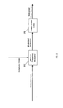
- a compensation filter 301 may be installed in the transmitting device in front of the phase locked loop 202 and the phase or frequency modulator 201.
- FIG. 3 depicts an exemplary signal path with a compensation filter.
- the compensation filter 301 may be a programmable hardware filter implemented in the ASIC or FPGA of, for example, the IDU 102.
- the compensation filter 301 may pre-distort the transmitted signal, such that after low pass filter distortion by the phase locked loop 202, the transmitted signal at an antenna connector port of the ODU 101 preserves the original signal from the IDU 102 with less distortion.
- the combined filter response of the compensation filter 301 and the phase locked loop 202 to the baseband signal may be equivalent to a Butterworth filter or any other appropriate function.
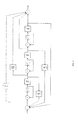
- the analog filter described by the compensation function may be implemented in the compensation filter 301 using canonical state variable implementation, where Fc may be the sampling frequency of the compensation filter 301.
- FIG. 4 depicts an exemplary digital state variable 3 rd order compensator for a compensation filter.
- the filter coefficients may be calculated according to equations as show in FIG. 4 , based on the values of the programmable coefficients or parameters of the transmitting device which may be stored in, for example, the ODU 101.
- FIG. 5 depicts an exemplary procedure for installing a compensation filter.
- parameters may be read from a transmitter.
- the compensation filter 301 may be installed in transmitting device, such as a VSAT.
- the compensation filter 301 may be installed in the IDU 103 of a VSAT.
- the IDU 103 is installed and connected to the ODU 101 of the VSAT, the programmable coefficients and parameters stored in the ODU 101 may be read by the IDU 103.
- a compensation function may be derived.
- the compensation filter 301 may derive a compensation function, as described above, using the programmable coefficients and parameters.
- the compensation function may be, for, example, a 3 rd order compensation function derived based on a wanted frequency response and the frequency response of the phase locked loop 202.
- the derived compensation function may be implemented in the compensation filter.
- the compensation function may be implemented in the compensation filter 301 by setting the filter coefficients in the compensation filter based on the compensation function derived using the programmable coefficients and parameters for the receiving device, such as the ODU 101 of the VSAT.
- the programming may occur in the hardware of the compensation filter 301.
- a "computer” or “computer system” may be, for example and without limitation, either alone or in combination, a personal computer (PC), server-based computer, main frame, server, microcomputer, minicomputer, laptop, personal data assistant (PDA), cellular phone, pager, processor, including wireless and/or wire line varieties thereof, and/or any other computerized device capable of configuration for receiving, storing and/or processing data for standalone application and/or over a networked medium or media.
- Examples of communication media that can be employed include, without limitation, wireless data networks, wire line networks, and/or a variety of networked media.
- Computers and computer systems described herein may include operatively associated computer-readable media such as memory for storing software applications used in obtaining, processing, storing and/or communicating data. It can be appreciated that such memory can be internal, external, remote or local with respect to its operatively associated computer or computer system. Memory may also include any means for storing software or other instructions including, for example and without limitation, a hard disk, an optical disk, floppy disk, DVD, compact disc, memory stick, ROM (read only memory), RAM (random access memory), PROM (programmable ROM), EEPROM (extended erasable PROM), and/or other like computer-readable media.
- ROM read only memory
- RAM random access memory
- PROM programmable ROM
- EEPROM extended erasable PROM
- computer-readable media may include any medium capable of being a carrier for an electronic signal representative of data stored, communicated or processed in accordance with embodiments of the present invention.
- method steps described herein may be embodied or executed as instructions stored on a computer-readable medium or media.
- a single component may be replaced by multiple components, and multiple components may be replaced by a single component, to provide an element or structure or to perform a given function or functions. Except where such substitution would not be operative to practice certain embodiments of the present invention, such substitution is considered within the scope of the present invention.
Landscapes
- Stabilization Of Oscillater, Synchronisation, Frequency Synthesizers (AREA)
- Transmitters (AREA)
Abstract
Description
- Devices that transmit wireless signals, such as Very Small Aperture Terminals (VSATs) in satellite communication systems, and cellular devices, may transmit the wireless signals on phase modulated carriers. The fidelity of a phase modulated carrier which is passed through a phase locked loop may be degraded by the bandwidth of that phase locked loop. The phase locked loop may reduce the bandwidth of the transmitting device, resulting in poorer performance than could be achieved by the rest of the components in the signal path of the receiving device.
- It is an object of the present invention to provide an apparatus and method for phase locked loop bandwidth expansion.
- In accordance with an aspect of the present invention, an apparatus for PLL bandwidth expansion includes a compensation filter and a phase locked loop, where the compensation filter is programmed with a compensation function derived based on programmable coefficients and parameters of a transmitting device, a frequency response of the phase locked loop, and a wanted frequency response.
- Additional objects, advantages and novel features of the invention are set forth in part in the description which follows, and in part will become apparent to those skilled in the art upon examination of the following or may be learned by practice of the invention. The objects and advantages of the invention may be realized and attained by means of the instrumentalities and combinations particularly pointed out in the appended claims.
-
FIG. 1 depicts an exemplary VSAT with indoor unit (IDU) and outdoor unit (ODU); -
FIG. 2 depicts an exemplary signal path; -
FIG. 3 depicts an exemplary signal path with a compensation filter; -
FIG. 4 depicts an exemplarydigital state variable 3rd order compensator for a compensation filter; and -
FIG. 5 depicts an exemplary procedure for installing the coefficients of a compensation filter. - The limitation on bandwidth caused by the use of a phase locked loop in a transmitting device may be overcome by using a compensation filter in the signal path at the baseband modulator. The compensation filter may expand the bandwidth of the signal path, and thus eliminate the limitation imposed by the bandwidth of the phase locked loop.
- The compensation filter may be implemented in a transmitting device, such as, for example, a VSAT.
FIG. 1 depicts an exemplary VSAT with indoor unit (IDU) and outdoor unit (ODU). The ODU 101 may be, for example, a satellite dish in combination with electronics for signal processing. The IDU 103 may be a set top box including a receiver and a transmitter that may transmit a signal to the ODU 101 on a cable, such as thecoaxial cable 102, so that the ODU 101 can transmit the signal to, for example, a satellite. The IDU 103 may perform processing on the wireless signal to be transmitted by the ODU 101, including, for example, inserting data into the signal. The signal may carry any suitable type of data, such as, for example, television data, or IP traffic. The ODU 101 may receive and process the signal from the IDU 103, and may transmit the signal as a wireless signal carried on a phase modulated carrier to a satellite, using, for example, a satellite dish. -
FIG. 2 depicts an exemplary signal path in a transmitting device. The signal path in the transmitting device, for example, in a VSAT, may be implemented with any suitable combination of hardware and software, including, for example, an application-specific integrated circuit (ASIC) or field programmable gate array (FPGA). The signal path may include a phase orfrequency modulator 201 which may receive a reference signal which may then be modulated by an input data signal to produce a modulated signal, which may then be used as a modulated reference into a phase lockedloop 202. The phase lockedloop 202 may reside, for example, in the ODU 101 or the IDU 103 of a VSAT. The output of the phase lockedloop 202 may be given by the transfer function:
where


and
where s may be the Laplace transform operator (jw), and a, b, Kvco , K φ, N, A, ξ, wn may be programmable coefficients or parameters of the transmitting device, for example, of theODU 101, and may be stored on the transmitting device at the time of manufacture. a may represent a "zero", b may represent a "pole", Kvco may represent VCO gain, K φ may represent phase detector gain, N may represent a variable divider value, A may represent a gain value, ξ may represent a damping factor, and wn , may represent a 2nd order filter natural frequency. Exemplary values for the programmable coefficients may be A=0.53826, Kvco =2π·375e 6,
- The magnitude response of the phase locked
loop 202 may cause the phase locked loop 203 to act as a lowpass filter, with a passband limit less than some of the typical signals that may be received by the ODU 101. The lowpass property of the phase lockedloop 202 may distort the transmitted signals heavily when signal bandwidth is wider than the filter bandwidth of the phase lockedloop 202. This may result in the phase lockedloop 202 limiting the overall bandwidth of the receiving device. - A
compensation filter 301 may be installed in the transmitting device in front of the phase lockedloop 202 and the phase orfrequency modulator 201.FIG. 3 depicts an exemplary signal path with a compensation filter. Thecompensation filter 301 may be a programmable hardware filter implemented in the ASIC or FPGA of, for example, the IDU 102. - The
compensation filter 301 may pre-distort the transmitted signal, such that after low pass filter distortion by the phase lockedloop 202, the transmitted signal at an antenna connector port of the ODU 101 preserves the original signal from the IDU 102 with less distortion. The combined filter response of thecompensation filter 301 and the phase lockedloop 202 to the baseband signal may be equivalent to a Butterworth filter or any other appropriate function. - The desired response of the combination of the
compensation filter 301 and the phase lockedloop 202, Freq(s), may be:
where wa may be the wanted bandwidth in radians/Hertz, and where, for a Butterworth response, b 3 may be 2.6, b 2 may be 3.4, and b 1 may be 2.6. By dividing the desired response by the response of the phase lockedloop 202, the fifth order compensation function, Fcomp(s), for thecompensation filter 301 may be derived as:
where y 0=wa 4,
y 1=b 1·wa 3,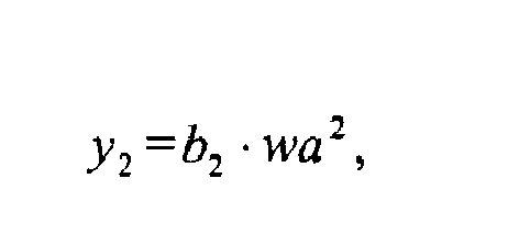


and
- To simplify implementation of the
compensation filter 301, wn may be assumed to be very large, which may allow the 4th and 5th order terms to be ignored. The phase lockedloop 202 frequency response may be approximated, for example, by:


and
- The desired second order frequency response, Freq(s), may be

where for a Butterworth response ξ may be equal to 0.707.
By dividing the desired response by the response of the phase lockedloop 202, the third order compensation function, Fcomp(s), for thecompensation filter 301 may be derived as:
where d 0=wa 2


and
- The analog filter described by the compensation function may be implemented in the
compensation filter 301 using canonical state variable implementation, where Fc may be the sampling frequency of thecompensation filter 301.FIG. 4 depicts an exemplarydigital state variable 3rd order compensator for a compensation filter. The filter coefficients may be calculated according to equations as show inFIG. 4 , based on the values of the programmable coefficients or parameters of the transmitting device which may be stored in, for example, the ODU 101. -
FIG. 5 depicts an exemplary procedure for installing a compensation filter. Inblock 501, parameters may be read from a transmitter. Thecompensation filter 301 may be installed in transmitting device, such as a VSAT. For example, thecompensation filter 301 may be installed in theIDU 103 of a VSAT. When theIDU 103 is installed and connected to theODU 101 of the VSAT, the programmable coefficients and parameters stored in theODU 101 may be read by theIDU 103. - In
block 502, a compensation function may be derived. For example, thecompensation filter 301 may derive a compensation function, as described above, using the programmable coefficients and parameters. The compensation function may be, for, example, a 3rd order compensation function derived based on a wanted frequency response and the frequency response of the phase lockedloop 202. - In
block 503, the derived compensation function may be implemented in the compensation filter. For example, the compensation function may be implemented in thecompensation filter 301 by setting the filter coefficients in the compensation filter based on the compensation function derived using the programmable coefficients and parameters for the receiving device, such as theODU 101 of the VSAT. The programming may occur in the hardware of thecompensation filter 301. - As used herein, a "computer" or "computer system" may be, for example and without limitation, either alone or in combination, a personal computer (PC), server-based computer, main frame, server, microcomputer, minicomputer, laptop, personal data assistant (PDA), cellular phone, pager, processor, including wireless and/or wire line varieties thereof, and/or any other computerized device capable of configuration for receiving, storing and/or processing data for standalone application and/or over a networked medium or media. Examples of communication media that can be employed include, without limitation, wireless data networks, wire line networks, and/or a variety of networked media.
- Computers and computer systems described herein may include operatively associated computer-readable media such as memory for storing software applications used in obtaining, processing, storing and/or communicating data. It can be appreciated that such memory can be internal, external, remote or local with respect to its operatively associated computer or computer system. Memory may also include any means for storing software or other instructions including, for example and without limitation, a hard disk, an optical disk, floppy disk, DVD, compact disc, memory stick, ROM (read only memory), RAM (random access memory), PROM (programmable ROM), EEPROM (extended erasable PROM), and/or other like computer-readable media.
- In general, computer-readable media may include any medium capable of being a carrier for an electronic signal representative of data stored, communicated or processed in accordance with embodiments of the present invention. Where applicable, method steps described herein may be embodied or executed as instructions stored on a computer-readable medium or media.
- It is to be understood that the figures and descriptions of the present invention have been simplified to illustrate elements that are relevant for a clear understanding of the present invention, while eliminating, for purposes of clarity, other elements. Those of ordinary skill in the art will recognize, however, that these and other elements may be desirable. However, because such elements are well known in the art, and because they do not facilitate a better understanding of the present invention, a discussion of such elements is not provided herein. It should be appreciated that the figures are presented for illustrative purposes and not as construction drawings. Omitted details and modifications or alternative embodiments are within the purview of persons of ordinary skill in the art.
- It can be appreciated that, in certain aspects of the present invention, a single component may be replaced by multiple components, and multiple components may be replaced by a single component, to provide an element or structure or to perform a given function or functions. Except where such substitution would not be operative to practice certain embodiments of the present invention, such substitution is considered within the scope of the present invention.
- The examples presented herein are intended to illustrate potential and specific implementations of the present invention. It can be appreciated that the examples are intended primarily for purposes of illustration of the invention for those skilled in the art. The diagrams depicted herein are provided by way of example. There may be variations to these diagrams or the operations described herein without departing from the spirit of the invention. For instance, in certain cases, method steps or operations may be performed or executed in differing order, or operations may be added, deleted or modified.
- Furthermore, whereas particular embodiments of the invention have been described herein for the purpose of illustrating the invention and not for the purpose of limiting the same, it will be appreciated by those of ordinary skill in the art that numerous variations of the details, materials and arrangement of elements, steps, structures, and/or parts may be made within the principle and scope of the invention without departing from the invention as described in the following claims.
Claims (20)
- An apparatus for PLL bandwidth expansion comprising:a compensation filter configured to be programmed with a compensation function derived based on programmable coefficients and parameters of a transmitting device.
- The apparatus of claim 1, wherein the compensation filter is installed in front of a phase locked loop.
- The apparatus of claim 1, wherein the derivation of the compensation function is also based on a frequency response of a phase locked loop and a wanted frequency response.
- The apparatus of claim 1, wherein the compensation filter is programmed with the compensation function by programming filter coefficients of a digital state variable 3rd order or higher compensator.
- The apparatus of claim 1, wherein the compensation filter is one of: an application specific integrated circuit, a field programmable gate array, and a combination of an application specific integrated circuit and a filed programmable gate array.
- The apparatus of claim 1, wherein the transmitting device is a VSAT.
- The apparatus of claim 1, wherein the compensation filter is programmed with the compensation function by programming filter coefficients of a filter comprising a filter topology.
- An apparatus for PLL bandwidth expansion comprising:a compensation filter; anda phase locked loop,wherein the compensation filter is programmed with a compensation function derived based on programmable coefficients and parameters of a transmitting device, a frequency response of the phase locked loop, and a wanted frequency response.
- The apparatus of claim 8, wherein the compensation function is a function for the wanted frequency response divided by a function for the frequency response of the phase locked loop.
- The apparatus of claim 8, wherein the compensation function is one of: a 5th order function, a 4th order function, a 3rd order function, a 2nd order function and a 1st order function.
- The apparatus of claim 8, wherein the compensation filter and the phase locked loop in combination produce a Butterworth response.
- The apparatus of claim 8, wherein the transmitting device is a VSAT, and wherein the programmable coefficients and parameters are stored in an outdoor unit of the VSAT.
- The apparatus of claim 8, wherein the compensation filter is programmed with the compensation function by programming filter coefficients of digital state variable 3rd order or higher compensator.
- A method for PLL bandwidth expansion comprising:determining programmable coefficients and parameters of a transmitting device;deriving a compensation function based on the programmable coefficients and parameters; andimplementing the compensation function.
- The method of claim 14, wherein determining programmable coefficients and parameters of a transmitting device further comprises reading the programmable coefficients and parameters stored on the transmitting device.
- The method of claim 14, wherein deriving a compensation function based on the programmable coefficients and parameters further comprises:determining a function for a wanted frequency response;determining a function for a frequency response of a phase locked loop; anddividing the function for the wanted frequency response by the function for the frequency response of the phase locked loop.
- The method of claim 14, wherein the compensation function is one of: a 5th order function, a 4th order function, a 3rd order function, a 2nd order function and a 1st order function.
- The method of claim 14, wherein implementing the compensation function further comprises programming filter coefficients of a digital state variable 3rd order or higher compensator.
- The method of claim 18, wherein the digital state variable 3rd order compensator is implemented in a field programmable gate array.
- The method of claim 18, wherein the digital state variable 3rd order compensator is implemented in an application specific integrated circuit.
Applications Claiming Priority (1)
| Application Number | Priority Date | Filing Date | Title |
|---|---|---|---|
| US13/400,959 US9099960B2 (en) | 2012-02-21 | 2012-02-21 | Apparatus and method for phase locked loop bandwidth expansion |
Publications (2)
| Publication Number | Publication Date |
|---|---|
| EP2632042A1 true EP2632042A1 (en) | 2013-08-28 |
| EP2632042B1 EP2632042B1 (en) | 2019-05-29 |
Family
ID=47722154
Family Applications (1)
| Application Number | Title | Priority Date | Filing Date |
|---|---|---|---|
| EP13155847.0A Active EP2632042B1 (en) | 2012-02-21 | 2013-02-19 | Apparatus and method for phase locked loop bandwidth expansion |
Country Status (3)
| Country | Link |
|---|---|
| US (2) | US9099960B2 (en) |
| EP (1) | EP2632042B1 (en) |
| BR (1) | BR102013003756B1 (en) |
Families Citing this family (2)
| Publication number | Priority date | Publication date | Assignee | Title |
|---|---|---|---|---|
| US9537492B2 (en) * | 2014-06-20 | 2017-01-03 | Analog Devices, Inc. | Sampled analog loop filter for phase locked loops |
| US10728015B1 (en) | 2019-06-06 | 2020-07-28 | Qualcomm Incorporated | Adaptive phase-locked loop bandwidth control |
Citations (4)
| Publication number | Priority date | Publication date | Assignee | Title |
|---|---|---|---|---|
| WO1998034339A1 (en) * | 1997-01-31 | 1998-08-06 | Massachusetts Institute Of Technology | Digital compensation for wideband modulation of a phase locked loop frequency synthesizer |
| WO1999014850A1 (en) * | 1997-09-16 | 1999-03-25 | Telefonaktiebolaget Lm Ericsson (Publ) | A compensated δς controlled phase locked loop modulator |
| US6833767B1 (en) * | 2003-03-28 | 2004-12-21 | National Semiconductor Corporation | Frequency synthesizer using digital pre-distortion and method |
| EP1583224A1 (en) * | 2003-01-08 | 2005-10-05 | Matsushita Electric Industrial Co., Ltd. | Modulator and correction method thereof |
Family Cites Families (9)
| Publication number | Priority date | Publication date | Assignee | Title |
|---|---|---|---|---|
| JPS62279758A (en) * | 1986-05-29 | 1987-12-04 | Nec Corp | Driving system for burst timing of phase modulator |
| US5432723A (en) * | 1993-12-02 | 1995-07-11 | Motorola, Inc. | Parallel infinite impulse response (IIR) filter with low quantization effects and method therefor |
| US6366620B1 (en) * | 1994-12-13 | 2002-04-02 | Hughes Electronics Corporation | VSAT system |
| US6097765A (en) * | 1995-09-05 | 2000-08-01 | Hughes Electronics Corporation | Method and apparatus for performing digital fractional minimum shift key modulation for a very small aperture terminal |
| US6671863B2 (en) * | 2002-02-14 | 2003-12-30 | Sun Microsystems, Inc. | Optimization of loop bandwidth for a phase locked loop |
| US7010265B2 (en) * | 2002-05-22 | 2006-03-07 | Microsoft Corporation | Satellite receiving system with transmodulating outdoor unit |
| US6806780B2 (en) * | 2003-03-13 | 2004-10-19 | Texas Instruments Incorporated | Efficient modulation compensation of sigma delta fractional phase locked loop |
| US7352249B2 (en) * | 2003-10-03 | 2008-04-01 | Analog Devices, Inc. | Phase-locked loop bandwidth calibration circuit and method thereof |
| US7502602B2 (en) * | 2005-07-19 | 2009-03-10 | Intel Corporation | Method and apparatus to compensate loop error of phase locked loop |
-
2012
- 2012-02-21 US US13/400,959 patent/US9099960B2/en active Active
-
2013
- 2013-02-18 BR BR102013003756-7A patent/BR102013003756B1/en active IP Right Grant
- 2013-02-19 EP EP13155847.0A patent/EP2632042B1/en active Active
-
2015
- 2015-08-03 US US14/816,448 patent/US9590645B2/en active Active
Patent Citations (4)
| Publication number | Priority date | Publication date | Assignee | Title |
|---|---|---|---|---|
| WO1998034339A1 (en) * | 1997-01-31 | 1998-08-06 | Massachusetts Institute Of Technology | Digital compensation for wideband modulation of a phase locked loop frequency synthesizer |
| WO1999014850A1 (en) * | 1997-09-16 | 1999-03-25 | Telefonaktiebolaget Lm Ericsson (Publ) | A compensated δς controlled phase locked loop modulator |
| EP1583224A1 (en) * | 2003-01-08 | 2005-10-05 | Matsushita Electric Industrial Co., Ltd. | Modulator and correction method thereof |
| US6833767B1 (en) * | 2003-03-28 | 2004-12-21 | National Semiconductor Corporation | Frequency synthesizer using digital pre-distortion and method |
Also Published As
| Publication number | Publication date |
|---|---|
| US20160065228A1 (en) | 2016-03-03 |
| US20130214830A1 (en) | 2013-08-22 |
| US9099960B2 (en) | 2015-08-04 |
| EP2632042B1 (en) | 2019-05-29 |
| US9590645B2 (en) | 2017-03-07 |
| BR102013003756A2 (en) | 2015-09-08 |
| BR102013003756B1 (en) | 2022-08-23 |
Similar Documents
| Publication | Publication Date | Title |
|---|---|---|
| CN107425922B (en) | A carrier frequency offset compensation circuit and method for inter-satellite optical communication | |
| KR20250005517A (en) | Apparatus and method for compensating phase fluctuations | |
| US11212017B2 (en) | Phase-locked loop (PLL) calibration | |
| US9722831B2 (en) | Carrier frequency offset processing method and apparatus and receiver | |
| CN107104739A (en) | A kind of ultra-broadband digital laser phase-locked loop device and phase-lock technique | |
| CN103916199B (en) | The time delay of a kind of aerial signal and phase adjusting apparatus and method | |
| US9590645B2 (en) | Apparatus and method for phase locked loop bandwidth expansion | |
| US20180069554A1 (en) | Clock and data recovery module | |
| US11316549B2 (en) | Radio frequency transmitting and receiving devices and unmanned aerial vehicle system | |
| US12237856B2 (en) | Q-band block down converter | |
| US10009203B1 (en) | Small-footprint digital receiver for extracting narrowband frequency-slices | |
| US20150171874A1 (en) | Phase locked loop (pll) apparatus and operating method of pll apparatus | |
| GB2545028A (en) | Receiver with automatic gain control by an alternating current closed loop | |
| US11283456B2 (en) | Apparatuses for generating an oscillation signal | |
| EP4694047A1 (en) | Communication method, apparatus, device, system, and readable storage medium | |
| CN112600572B (en) | Receiver, receiving method and related equipment | |
| US9645972B2 (en) | Butterfly channelizer | |
| US11025230B2 (en) | Filter that minimizes in-band noise and maximizes detection sensitivity of exponentially-modulated signals | |
| CN117335819B (en) | Multi-channel correction method and system for multifunctional integration of baseband and intermediate frequency | |
| WO2015143274A1 (en) | A filter that minimizes in-band noise and maximizes detection sensitivity of exponentially-modulated signals | |
| CN105245242A (en) | X-band spaceborne phase lock receiver | |
| Paik et al. | Design and implementation of Nano Satellite data receiver using SDR | |
| CN105282087A (en) | High-order modulation data symbol phase compensation method, device and circuit | |
| US20100296502A1 (en) | I-q mismatch compensation | |
| Wölfel et al. | Self-calibrating highly integrated radio frequency front-end for parallel π/4 DQPSK decoding |
Legal Events
| Date | Code | Title | Description |
|---|---|---|---|
| PUAI | Public reference made under article 153(3) epc to a published international application that has entered the european phase |
Free format text: ORIGINAL CODE: 0009012 |
|
| 17P | Request for examination filed |
Effective date: 20130219 |
|
| AK | Designated contracting states |
Kind code of ref document: A1 Designated state(s): AL AT BE BG CH CY CZ DE DK EE ES FI FR GB GR HR HU IE IS IT LI LT LU LV MC MK MT NL NO PL PT RO RS SE SI SK SM TR |
|
| AX | Request for extension of the european patent |
Extension state: BA ME |
|
| STAA | Information on the status of an ep patent application or granted ep patent |
Free format text: STATUS: EXAMINATION IS IN PROGRESS |
|
| 17Q | First examination report despatched |
Effective date: 20171031 |
|
| REG | Reference to a national code |
Ref country code: DE Ref legal event code: R079 Ref document number: 602013055963 Country of ref document: DE Free format text: PREVIOUS MAIN CLASS: H03C0003080000 Ipc: H03C0003090000 |
|
| GRAP | Despatch of communication of intention to grant a patent |
Free format text: ORIGINAL CODE: EPIDOSNIGR1 |
|
| STAA | Information on the status of an ep patent application or granted ep patent |
Free format text: STATUS: GRANT OF PATENT IS INTENDED |
|
| RIC1 | Information provided on ipc code assigned before grant |
Ipc: H03C 3/08 20060101ALI20181114BHEP Ipc: H03L 7/10 20060101ALI20181114BHEP Ipc: H03L 7/08 20060101ALI20181114BHEP Ipc: H03C 3/09 20060101AFI20181114BHEP |
|
| INTG | Intention to grant announced |
Effective date: 20181214 |
|
| GRAS | Grant fee paid |
Free format text: ORIGINAL CODE: EPIDOSNIGR3 |
|
| GRAA | (expected) grant |
Free format text: ORIGINAL CODE: 0009210 |
|
| STAA | Information on the status of an ep patent application or granted ep patent |
Free format text: STATUS: THE PATENT HAS BEEN GRANTED |
|
| AK | Designated contracting states |
Kind code of ref document: B1 Designated state(s): AL AT BE BG CH CY CZ DE DK EE ES FI FR GB GR HR HU IE IS IT LI LT LU LV MC MK MT NL NO PL PT RO RS SE SI SK SM TR |
|
| REG | Reference to a national code |
Ref country code: GB Ref legal event code: FG4D |
|
| REG | Reference to a national code |
Ref country code: CH Ref legal event code: EP |
|
| REG | Reference to a national code |
Ref country code: AT Ref legal event code: REF Ref document number: 1138857 Country of ref document: AT Kind code of ref document: T Effective date: 20190615 |
|
| REG | Reference to a national code |
Ref country code: DE Ref legal event code: R096 Ref document number: 602013055963 Country of ref document: DE |
|
| REG | Reference to a national code |
Ref country code: IE Ref legal event code: FG4D |
|
| REG | Reference to a national code |
Ref country code: NL Ref legal event code: MP Effective date: 20190529 |
|
| REG | Reference to a national code |
Ref country code: LT Ref legal event code: MG4D |
|
| PG25 | Lapsed in a contracting state [announced via postgrant information from national office to epo] |
Ref country code: AL Free format text: LAPSE BECAUSE OF FAILURE TO SUBMIT A TRANSLATION OF THE DESCRIPTION OR TO PAY THE FEE WITHIN THE PRESCRIBED TIME-LIMIT Effective date: 20190529 Ref country code: FI Free format text: LAPSE BECAUSE OF FAILURE TO SUBMIT A TRANSLATION OF THE DESCRIPTION OR TO PAY THE FEE WITHIN THE PRESCRIBED TIME-LIMIT Effective date: 20190529 Ref country code: LT Free format text: LAPSE BECAUSE OF FAILURE TO SUBMIT A TRANSLATION OF THE DESCRIPTION OR TO PAY THE FEE WITHIN THE PRESCRIBED TIME-LIMIT Effective date: 20190529 Ref country code: SE Free format text: LAPSE BECAUSE OF FAILURE TO SUBMIT A TRANSLATION OF THE DESCRIPTION OR TO PAY THE FEE WITHIN THE PRESCRIBED TIME-LIMIT Effective date: 20190529 Ref country code: NO Free format text: LAPSE BECAUSE OF FAILURE TO SUBMIT A TRANSLATION OF THE DESCRIPTION OR TO PAY THE FEE WITHIN THE PRESCRIBED TIME-LIMIT Effective date: 20190829 Ref country code: ES Free format text: LAPSE BECAUSE OF FAILURE TO SUBMIT A TRANSLATION OF THE DESCRIPTION OR TO PAY THE FEE WITHIN THE PRESCRIBED TIME-LIMIT Effective date: 20190529 Ref country code: PT Free format text: LAPSE BECAUSE OF FAILURE TO SUBMIT A TRANSLATION OF THE DESCRIPTION OR TO PAY THE FEE WITHIN THE PRESCRIBED TIME-LIMIT Effective date: 20190930 Ref country code: HR Free format text: LAPSE BECAUSE OF FAILURE TO SUBMIT A TRANSLATION OF THE DESCRIPTION OR TO PAY THE FEE WITHIN THE PRESCRIBED TIME-LIMIT Effective date: 20190529 |
|
| PG25 | Lapsed in a contracting state [announced via postgrant information from national office to epo] |
Ref country code: GR Free format text: LAPSE BECAUSE OF FAILURE TO SUBMIT A TRANSLATION OF THE DESCRIPTION OR TO PAY THE FEE WITHIN THE PRESCRIBED TIME-LIMIT Effective date: 20190830 Ref country code: BG Free format text: LAPSE BECAUSE OF FAILURE TO SUBMIT A TRANSLATION OF THE DESCRIPTION OR TO PAY THE FEE WITHIN THE PRESCRIBED TIME-LIMIT Effective date: 20190829 Ref country code: RS Free format text: LAPSE BECAUSE OF FAILURE TO SUBMIT A TRANSLATION OF THE DESCRIPTION OR TO PAY THE FEE WITHIN THE PRESCRIBED TIME-LIMIT Effective date: 20190529 Ref country code: LV Free format text: LAPSE BECAUSE OF FAILURE TO SUBMIT A TRANSLATION OF THE DESCRIPTION OR TO PAY THE FEE WITHIN THE PRESCRIBED TIME-LIMIT Effective date: 20190529 |
|
| REG | Reference to a national code |
Ref country code: AT Ref legal event code: MK05 Ref document number: 1138857 Country of ref document: AT Kind code of ref document: T Effective date: 20190529 |
|
| PG25 | Lapsed in a contracting state [announced via postgrant information from national office to epo] |
Ref country code: CZ Free format text: LAPSE BECAUSE OF FAILURE TO SUBMIT A TRANSLATION OF THE DESCRIPTION OR TO PAY THE FEE WITHIN THE PRESCRIBED TIME-LIMIT Effective date: 20190529 Ref country code: RO Free format text: LAPSE BECAUSE OF FAILURE TO SUBMIT A TRANSLATION OF THE DESCRIPTION OR TO PAY THE FEE WITHIN THE PRESCRIBED TIME-LIMIT Effective date: 20190529 Ref country code: NL Free format text: LAPSE BECAUSE OF FAILURE TO SUBMIT A TRANSLATION OF THE DESCRIPTION OR TO PAY THE FEE WITHIN THE PRESCRIBED TIME-LIMIT Effective date: 20190529 Ref country code: AT Free format text: LAPSE BECAUSE OF FAILURE TO SUBMIT A TRANSLATION OF THE DESCRIPTION OR TO PAY THE FEE WITHIN THE PRESCRIBED TIME-LIMIT Effective date: 20190529 Ref country code: EE Free format text: LAPSE BECAUSE OF FAILURE TO SUBMIT A TRANSLATION OF THE DESCRIPTION OR TO PAY THE FEE WITHIN THE PRESCRIBED TIME-LIMIT Effective date: 20190529 Ref country code: DK Free format text: LAPSE BECAUSE OF FAILURE TO SUBMIT A TRANSLATION OF THE DESCRIPTION OR TO PAY THE FEE WITHIN THE PRESCRIBED TIME-LIMIT Effective date: 20190529 Ref country code: SK Free format text: LAPSE BECAUSE OF FAILURE TO SUBMIT A TRANSLATION OF THE DESCRIPTION OR TO PAY THE FEE WITHIN THE PRESCRIBED TIME-LIMIT Effective date: 20190529 |
|
| PG25 | Lapsed in a contracting state [announced via postgrant information from national office to epo] |
Ref country code: SM Free format text: LAPSE BECAUSE OF FAILURE TO SUBMIT A TRANSLATION OF THE DESCRIPTION OR TO PAY THE FEE WITHIN THE PRESCRIBED TIME-LIMIT Effective date: 20190529 Ref country code: IT Free format text: LAPSE BECAUSE OF FAILURE TO SUBMIT A TRANSLATION OF THE DESCRIPTION OR TO PAY THE FEE WITHIN THE PRESCRIBED TIME-LIMIT Effective date: 20190529 |
|
| REG | Reference to a national code |
Ref country code: DE Ref legal event code: R097 Ref document number: 602013055963 Country of ref document: DE |
|
| PG25 | Lapsed in a contracting state [announced via postgrant information from national office to epo] |
Ref country code: TR Free format text: LAPSE BECAUSE OF FAILURE TO SUBMIT A TRANSLATION OF THE DESCRIPTION OR TO PAY THE FEE WITHIN THE PRESCRIBED TIME-LIMIT Effective date: 20190529 |
|
| PLBE | No opposition filed within time limit |
Free format text: ORIGINAL CODE: 0009261 |
|
| STAA | Information on the status of an ep patent application or granted ep patent |
Free format text: STATUS: NO OPPOSITION FILED WITHIN TIME LIMIT |
|
| PG25 | Lapsed in a contracting state [announced via postgrant information from national office to epo] |
Ref country code: PL Free format text: LAPSE BECAUSE OF FAILURE TO SUBMIT A TRANSLATION OF THE DESCRIPTION OR TO PAY THE FEE WITHIN THE PRESCRIBED TIME-LIMIT Effective date: 20190529 |
|
| 26N | No opposition filed |
Effective date: 20200303 |
|
| PG25 | Lapsed in a contracting state [announced via postgrant information from national office to epo] |
Ref country code: SI Free format text: LAPSE BECAUSE OF FAILURE TO SUBMIT A TRANSLATION OF THE DESCRIPTION OR TO PAY THE FEE WITHIN THE PRESCRIBED TIME-LIMIT Effective date: 20190529 |
|
| REG | Reference to a national code |
Ref country code: CH Ref legal event code: PL |
|
| REG | Reference to a national code |
Ref country code: BE Ref legal event code: MM Effective date: 20200229 |
|
| PG25 | Lapsed in a contracting state [announced via postgrant information from national office to epo] |
Ref country code: LU Free format text: LAPSE BECAUSE OF NON-PAYMENT OF DUE FEES Effective date: 20200219 Ref country code: MC Free format text: LAPSE BECAUSE OF FAILURE TO SUBMIT A TRANSLATION OF THE DESCRIPTION OR TO PAY THE FEE WITHIN THE PRESCRIBED TIME-LIMIT Effective date: 20190529 |
|
| PG25 | Lapsed in a contracting state [announced via postgrant information from national office to epo] |
Ref country code: LI Free format text: LAPSE BECAUSE OF NON-PAYMENT OF DUE FEES Effective date: 20200229 Ref country code: CH Free format text: LAPSE BECAUSE OF NON-PAYMENT OF DUE FEES Effective date: 20200229 |
|
| PG25 | Lapsed in a contracting state [announced via postgrant information from national office to epo] |
Ref country code: IE Free format text: LAPSE BECAUSE OF NON-PAYMENT OF DUE FEES Effective date: 20200219 Ref country code: FR Free format text: LAPSE BECAUSE OF NON-PAYMENT OF DUE FEES Effective date: 20200229 |
|
| PG25 | Lapsed in a contracting state [announced via postgrant information from national office to epo] |
Ref country code: BE Free format text: LAPSE BECAUSE OF NON-PAYMENT OF DUE FEES Effective date: 20200229 |
|
| PG25 | Lapsed in a contracting state [announced via postgrant information from national office to epo] |
Ref country code: MT Free format text: LAPSE BECAUSE OF FAILURE TO SUBMIT A TRANSLATION OF THE DESCRIPTION OR TO PAY THE FEE WITHIN THE PRESCRIBED TIME-LIMIT Effective date: 20190529 Ref country code: CY Free format text: LAPSE BECAUSE OF FAILURE TO SUBMIT A TRANSLATION OF THE DESCRIPTION OR TO PAY THE FEE WITHIN THE PRESCRIBED TIME-LIMIT Effective date: 20190529 |
|
| PG25 | Lapsed in a contracting state [announced via postgrant information from national office to epo] |
Ref country code: MK Free format text: LAPSE BECAUSE OF FAILURE TO SUBMIT A TRANSLATION OF THE DESCRIPTION OR TO PAY THE FEE WITHIN THE PRESCRIBED TIME-LIMIT Effective date: 20190529 Ref country code: IS Free format text: LAPSE BECAUSE OF FAILURE TO SUBMIT A TRANSLATION OF THE DESCRIPTION OR TO PAY THE FEE WITHIN THE PRESCRIBED TIME-LIMIT Effective date: 20190929 |
|
| P01 | Opt-out of the competence of the unified patent court (upc) registered |
Effective date: 20230530 |
|
| PGFP | Annual fee paid to national office [announced via postgrant information from national office to epo] |
Ref country code: GB Payment date: 20260106 Year of fee payment: 14 |
|
| PGFP | Annual fee paid to national office [announced via postgrant information from national office to epo] |
Ref country code: DE Payment date: 20251224 Year of fee payment: 14 |