EP2624377A1 - Communication adapter having asymmetrical outer contacts springs or outer contact springs extending below the top surface of a printed circuit board - Google Patents
Communication adapter having asymmetrical outer contacts springs or outer contact springs extending below the top surface of a printed circuit board Download PDFInfo
- Publication number
- EP2624377A1 EP2624377A1 EP13152508.1A EP13152508A EP2624377A1 EP 2624377 A1 EP2624377 A1 EP 2624377A1 EP 13152508 A EP13152508 A EP 13152508A EP 2624377 A1 EP2624377 A1 EP 2624377A1
- Authority
- EP
- European Patent Office
- Prior art keywords
- circuit board
- printed circuit
- contact
- adapter
- contact spring
- Prior art date
- Legal status (The legal status is an assumption and is not a legal conclusion. Google has not performed a legal analysis and makes no representation as to the accuracy of the status listed.)
- Granted
Links
- 238000004891 communication Methods 0.000 title claims abstract description 92
- 238000005452 bending Methods 0.000 claims description 3
- 238000009413 insulation Methods 0.000 description 8
- 230000005540 biological transmission Effects 0.000 description 4
- 238000011161 development Methods 0.000 description 4
- QHZSDTDMQZPUKC-UHFFFAOYSA-N 3,5-dichlorobiphenyl Chemical compound ClC1=CC(Cl)=CC(C=2C=CC=CC=2)=C1 QHZSDTDMQZPUKC-UHFFFAOYSA-N 0.000 description 3
- 239000004020 conductor Substances 0.000 description 3
- 238000006073 displacement reaction Methods 0.000 description 3
- XEEYBQQBJWHFJM-UHFFFAOYSA-N Iron Chemical compound [Fe] XEEYBQQBJWHFJM-UHFFFAOYSA-N 0.000 description 2
- PXHVJJICTQNCMI-UHFFFAOYSA-N Nickel Chemical compound [Ni] PXHVJJICTQNCMI-UHFFFAOYSA-N 0.000 description 2
- 238000013461 design Methods 0.000 description 2
- 238000003780 insertion Methods 0.000 description 2
- 230000037431 insertion Effects 0.000 description 2
- 238000005259 measurement Methods 0.000 description 2
- BASFCYQUMIYNBI-UHFFFAOYSA-N platinum Chemical compound [Pt] BASFCYQUMIYNBI-UHFFFAOYSA-N 0.000 description 2
- 229910001369 Brass Inorganic materials 0.000 description 1
- 229910000906 Bronze Inorganic materials 0.000 description 1
- RYGMFSIKBFXOCR-UHFFFAOYSA-N Copper Chemical compound [Cu] RYGMFSIKBFXOCR-UHFFFAOYSA-N 0.000 description 1
- BQCADISMDOOEFD-UHFFFAOYSA-N Silver Chemical compound [Ag] BQCADISMDOOEFD-UHFFFAOYSA-N 0.000 description 1
- 229910000831 Steel Inorganic materials 0.000 description 1
- 239000010951 brass Substances 0.000 description 1
- 239000010974 bronze Substances 0.000 description 1
- 230000006835 compression Effects 0.000 description 1
- 238000007906 compression Methods 0.000 description 1
- 229910052802 copper Inorganic materials 0.000 description 1
- 239000010949 copper Substances 0.000 description 1
- KUNSUQLRTQLHQQ-UHFFFAOYSA-N copper tin Chemical compound [Cu].[Sn] KUNSUQLRTQLHQQ-UHFFFAOYSA-N 0.000 description 1
- 239000000428 dust Substances 0.000 description 1
- 239000012777 electrically insulating material Substances 0.000 description 1
- 238000005516 engineering process Methods 0.000 description 1
- PCHJSUWPFVWCPO-UHFFFAOYSA-N gold Chemical compound [Au] PCHJSUWPFVWCPO-UHFFFAOYSA-N 0.000 description 1
- 229910052737 gold Inorganic materials 0.000 description 1
- 239000010931 gold Substances 0.000 description 1
- 229910052742 iron Inorganic materials 0.000 description 1
- 238000004519 manufacturing process Methods 0.000 description 1
- 230000013011 mating Effects 0.000 description 1
- 239000002184 metal Substances 0.000 description 1
- 229910052751 metal Inorganic materials 0.000 description 1
- 238000012986 modification Methods 0.000 description 1
- 230000004048 modification Effects 0.000 description 1
- 229910052759 nickel Inorganic materials 0.000 description 1
- 229920003023 plastic Polymers 0.000 description 1
- 239000004033 plastic Substances 0.000 description 1
- 229910052697 platinum Inorganic materials 0.000 description 1
- 150000003071 polychlorinated biphenyls Chemical class 0.000 description 1
- 238000012545 processing Methods 0.000 description 1
- 229910052709 silver Inorganic materials 0.000 description 1
- 239000004332 silver Substances 0.000 description 1
- 229910001220 stainless steel Inorganic materials 0.000 description 1
- 239000010935 stainless steel Substances 0.000 description 1
- 239000010959 steel Substances 0.000 description 1
Images


Classifications
-
- H—ELECTRICITY
- H01—ELECTRIC ELEMENTS
- H01R—ELECTRICALLY-CONDUCTIVE CONNECTIONS; STRUCTURAL ASSOCIATIONS OF A PLURALITY OF MUTUALLY-INSULATED ELECTRICAL CONNECTING ELEMENTS; COUPLING DEVICES; CURRENT COLLECTORS
- H01R24/00—Two-part coupling devices, or either of their cooperating parts, characterised by their overall structure
- H01R24/60—Contacts spaced along planar side wall transverse to longitudinal axis of engagement
- H01R24/62—Sliding engagements with one side only, e.g. modular jack coupling devices
- H01R24/64—Sliding engagements with one side only, e.g. modular jack coupling devices for high frequency, e.g. RJ 45
-
- H—ELECTRICITY
- H01—ELECTRIC ELEMENTS
- H01R—ELECTRICALLY-CONDUCTIVE CONNECTIONS; STRUCTURAL ASSOCIATIONS OF A PLURALITY OF MUTUALLY-INSULATED ELECTRICAL CONNECTING ELEMENTS; COUPLING DEVICES; CURRENT COLLECTORS
- H01R2201/00—Connectors or connections adapted for particular applications
- H01R2201/04—Connectors or connections adapted for particular applications for network, e.g. LAN connectors
Definitions
- the invention relates to a modular communications adapter for receiving an electrical communications plug-type connector as defined in the preamble of claim 1 or claim 12.
- the invention deals with electrical contact arrangement for telecommunication and data processing technology, has high-frequency electrical contacts electrically and mechanically connected with printed circuit board, where electrical contacts include contact area.
- the connection for high frequency data transmission refers to the RJ45 specification (IEC 60603-7).
- the RJ45 specification describes the faces of the RJ45 communications plug and the RJ45 communications adapter.
- the RJ45 specification requires eight (8) contact pins for data transmission.
- the RJ45 communications plug has eight (8) relatively stiff contacts separated by separators and the RJ45 communications adapter has eight (8) relatively flexible contact springs to connect with the relatively stiff contacts of the RJ45 communications plug.
- the aim is to use short contact springs within the RJ45 communications adapter for a good high frequency data transmission. On the other hand this contact spring needs a mechanical flexibility.
- the RJ45 communications adapter is also compatible to a RJ11 communications plug having only six (6) contacts.
- the insertion of a RJ11 communications plug into a RJ45 communications adapter causes more movement of the outer contact springs of the RJ45 communications adapter, because they do not encounter a contact of the RJ11 communications plug and are pressed down much more by the separators of the RJ11 communications plug. For this reason the outer contact springs have to be more flexible than the others. If the outer contact springs of a RJ45 communications adapter would not have a higher appropriate flexibility, the insertion of a RJ11 communications plug would destroy them. No safe connection could be realized. This case has to be avoided.
- a modular communications adapter as defined in the preamble of claim 1 or claim 13 is disclosed in the prior art document US 6,530,810 B2 .
- the present invention is based on the object of providing a novel modular communications adapter.
- the object of the invention is according to a first aspect of the invention achieved by a communications adapter according to claim 1.
- the outer contact springs are asymmetrical along the spring central axis of the same, while the inner contact springs are symmetrical along the spring central axis of the same. This provides an appropriate flexibility for the outer contact springs in order to avoid that the outer contact springs become damaged in case a communications plug becomes inserted into the communications adapter which is not of the same type. Especially, outer contact springs of a RJ45 communications adapter will not damaged when inserting a RJ11 communications plug into the same.
- each inner contact spring has a first length and each outer contact spring has a second length longer than the first length, wherein the first length and the second length being measured along the respective contact spring from an intersection of the respective fixed end of the respective contact spring and a surface of the printed circuit board to the respective contact end of the respective contact spring.
- each inner contact spring includes at least two bends, wherein each outer contact spring includes at least one more bend than the inner contact springs. This provides a further improved flexibility for the outer contact springs.
- each outer contact spring is wider at the fixed end than at the contact end for providing a larger elastic bending range than the inner contact springs.
- each outer contact spring has multiple widths along the length of the spring, the multiple widths including a first width at the fixed end that tapers to a second width smaller than the first width, the second width tapering to a third width that is larger than the second width but smaller than the first width, the third width tapering to the final width that is smaller than the first, second and third widths. This provides a further improved flexibility for the outer contact springs.
- the printed circuit board includes a top surface and a bottom surface, wherein each outer contact spring extends below the top surface in one respective location.
- the longer, asymmetrical outer springs have a space in the printed circuit board where they can move into.
- the object of the invention is according to a second aspect of the invention achieved by a communications adapter according to claim 12.
- the printed circuit board includes a top surface and a bottom surface, wherein each second contact spring extends below the top surface in one respective location at least in a mated condition of the same.
- the outer springs have a space in the printed circuit board where they can move into.
- each second contact spring extends below the top surface in one respective location in a mated condition and in an unmated condition of the same.
- each location includes at least one conductive aperture for receiving the fixed end of the respective second contact spring and at least one cut-out for receiving at least one of the bends of the respective second contact spring.
- the novel communications adapter was developed for the Next Generation of applicants existing Product S500 being a RJ45 communications adapter.
- a main part of that communications adapter is the contact spring.
- a new design of the contact spring is provided. Eight (8) contact springs mounted on a printed circuit board with a first end of the contact spring, with a second free end of the contact spring is directed away from the mounting location, the second end not contacting the printed circuit board.
- the first aspect deals with the mechanical flexibility of the outer springs.
- the outer contact springs have to be more bendable than the inner contact springs.
- the inner contact springs have the worst crosstalk behavior and need a minimum length.
- the printed circuit board includes locations proving space in the printed circuit board for the second contact springs, wherein each second contact spring extends in one said locations at least in a mated condition of the same.
- the more flexible outer contact springs have a space in the printed circuit board where they can move into when a communications plug becomes inserted into the communications adapter.
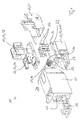
- Figure 1 shows an exploded view of an exemplary embodiment of a modular communications adapter according to the present invention
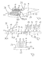
- Figure 2 shows a perspective view of a printed circuit board (PCB) having an array of contact springs
- FIG 3 shows a side view of the printed circuit board (PCB) of Figure 2 further having an array of insulation displacement connector (IDC) contacts;
- PCB printed circuit board
- IDC insulation displacement connector
- Figure 4 shows a front view of the printed circuit board of Figure 2 ;
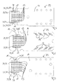
- Figures 5-7 show top views of different embodiments of printed circuit boards (PCB), wherein the PCBs of Figures 5-7 each have an array of contact springs, and whereby the PCB of Figures 6 further has an array IDC contacts;
- PCB printed circuit boards
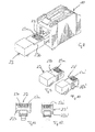
- Figure 8 shows a perspective assembly view of an RJ45 communications plug ready to insert into an embodiment of a RJ45 communications adapter
- FIGS 9,10 show perspective views of RJ45 and RJ11 communications plugs, for comparison
- Figures 11, 12 show front views of the communications plugs of Figures 9 and 10 ;
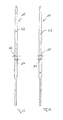
- Figures 13, 14 show front views of flat stampings of outer contact springs for the communications adapter
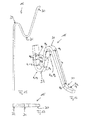
- Figure 15 shows a side view of a full, uninstalled outer contact spring for the communications adapter
- Figure 16 shows a partial perspective view of the contact spring of Figure 15 showing relative measurements along the length of the contact spring
- Figure 17 shows a top view of the contact spring of Figure 15 ;
- Figure 18 shows a side view of full, uninstalled inner contact spring for the communications adapter
- Figure 19 shows a front view of the contact springs of Figure 18 ;
- Figure 20 shows a top view of the contact spring of Figure 18 ;
- Figure 21 shows a partial perspective view of the contact spring of Figure 18 showing relative measurements along the length of the spring
- Figures 22-24 show perspective views of the different contact springs.
- RJ11 communications plug can be plugged into a RJ45 communications adapter without damaging the RJ45 communications adapter.
- the communications adapter is compatible with a RJ11 communications plug and a RJ45 communications plug. There is no additional part like e.g. a stopper needed.
- Outer contact springs of the communications adapter have more mechanical flexibility than inner contact springs of the communications adapter.
- the inner contact springs of the communications adapter are in contrast designed to allow high frequency data transmission of the communications adapter with less crosstalk.
- the necessary space for the contact springs of a communications adapter can be reduced. Due to this the dimension of the communications adapter becomes smaller.
- the manufacturing process is to assemble all spring contacts in one line at the same time. That reduces the assembly-effort and saves money.
- a modular communications adapter 10 consists of a housing 11 and a support part 12.
- the support part 12 includes an insulation body 13 that carries a printed circuit board (PCB) 14 with a plurality of contact springs 15, 16 and a plurality of insulation displacement connector (IDC) contacts 17.
- PCB printed circuit board
- IDC insulation displacement connector
- All contact springs 15, 16 of the communications adapter 10 stand side-by-side along one line.
- the IDC contacts 17 stand side-by-side along two parallel lines.
- the parallel lines in which the IDC contacts 17 stand run perpendicular to the line in which the contact springs 15, 16 are positioned.
- the insulation body 13 of the support part 12 comprises in the shown embodiment three elements, namely an upper holding element 18, a lower holding element 19 and a compression element 20.
- the three elements of the insulation body 13 are made from an electrically insulating material like plastics.
- the support part 12 further includes a shielding body 21.
- the shielding body 21 is made from an electrically conducting material like metal.
- Each contact spring 15, 16 is fixed with one end 22 in the PCB 14. This end 22 is also called fixed end 22.
- the other, opposite end 24 of the respective contact spring 15, 16 is free to connect stiff contacts 23a of a communications plug-type connector 23.
- the free end 24 is also called contact end 24.
- the fixed ends 22 of the contact springs 15, 16 define a linear array of fixed ends 22.
- the housing 11 of the communications adapter 10 comprises an opening 25 for receiving an electrical communications plug-type connector 23.
- the opening 25 of the housing 11 can be covered by a dust cap 26.
- the printed circuit board (PCB) 14 includes electrical traces for providing a plurality of electrical paths extending between a first end 38 of the printed circuit board 14 and a second end 39 of the printed circuit board 14.
- the fixed ends 22 of the contact springs 15, 16 are fixed to the first end 38 of the printed circuit board 14.
- the insulation displacement connector (IDC) contacts 17 are fixed to the second end 39 of the printed circuit board 14.
- the electrical traces of the PCB 14 provide electrical conductive paths between the contact springs 15, 16 and the IDC contacts 17.
- RJ45 communications plug-type connector 23 In case of a RJ45 communications plug-type connector 23, the same comprises eight (8) stiff contacts 23a (see Figures 8, 9, 11 ) hold by an insulation body 23b.
- the RJ45 communications adapter 10 for such a RJ45 communications plug-type connector 23 comprises eight (8) contact springs 15, 16, namely six (6) first, inner contact springs 15 and two (2) second, outer contact springs 16.
- the stiff contacts 23a contact the contact springs 15, 16.
- the first, inner contact springs 15 of the communications adapter are symmetrical along a first spring central axis X1 (see Figure 19 ), wherein the second, outer contact springs 16 of the communications adapter are asymmetrical along a second spring central axis X2 (see Figures 13 and 14).
- Figures 13, 14 show front views of flat stampings of outer contact springs 16.
- the second, outer contact springs 16 are asymmetrical along the second spring central axis X2 in such a way that the second, outer contact springs 16 are symmetrical in the region of the contact ends 24 of the same and asymmetrical in the region of the fixed ends 22 of the same.
- the second, outer contact springs 16 comprise in sections which provide the fixed ends 22 of the outer contact springs 16 the thickness d2 at a first side and the thickness d1 at a second side, wherein the thickness d2 is lager than the thickness d1
- the first side with the larger thickness d2 of the outer contact spring 16 is facing away from a respective neighboring inner contact spring 15.
- the second side with the smaller thickness d1 of the outer contact spring 16 is facing towards the respective neighboring inner contact spring 15.
- the asymmetric design of the second, outer contact springs 16 provides an appropriate flexibility for the outer contact springs 16 in order to avoid that the outer contact springs 16 become damaged in case a communications plug becomes inserted into the communications adapter 10 which is not of the same type.
- outer contact springs 16 of a RJ45 communications adapter 10 will not damaged when inserting a RJ11 communications plug 23' into the same.
- the second, outer contact springs 16 are asymmetrical along the respective spring central axis X2.
- Figures 13 and 22 shows an outer left contact spring 16 and
- Figures 14 and 24 shows an outer right contact spring 16.
- Both outer contact springs 16 are asymmetrical along a respective spring central axis X2.
- the outer right contact spring 16 of Figure 24 is a mirror image of the outer left contact spring 16 of Figure 22 along the respective central axes X2. Both outer contact springs 16 have about the same length.
- Figures 13 and 14 show front views of flat stampings of these two outer contact springs 16.
- the first, inner contact springs have a first length and the second, outer contact springs 16 have a second length longer than the first length. This provides a further improved flexibility for the outer contact springs 16.
- the first length and the second length is measured along the contact springs 15, 16 from an intersection of the respective fixed ends 22 and an upper or top surface 27 of the printed circuit board 14 to the respective contact ends 23.
- the second length may be up to 100% longer than the first length.
- the second length may be from 10% to 40% longer than the first length.
- the second length is from 20% to 30% longer than the first length.
- the second length may be from 25% to 30% longer than the first length.
- Each first, inner contact spring 15 includes at least two bends 28, 29 (see Figures 18 , 21, 23 ).
- Each second, outer contact spring 16 includes at least one more bend 30, 31, 32 (see Figures 15, 16 , 22, 24 ) than the first, inner contact springs 15. This provides a further improved flexibility for the outer contact springs 16.
- the contact ends 24 of the contact springs 15, 16 define a contact zone for making electrical contact with the electrical plug-type connector 23.
- the contact zone may include at least one bend 28, 30 on the contact springs 15, 16.
- the printed circuit board 14 includes the upper or top surface 27 and on the opposite side a lower or bottom surface 33.
- each second, outer contact spring 16 extends below the top surface 27 in one respective location 34 at least in a mated condition of the respective outer contact springs 16.
- the second, outer contact springs 16 may extend below the top surface 27 of the PCB 14 in the locations 34 in the mated condition and in an unmated condition.
- Each of said locations 34 includes one conductive aperture 35 for receiving the fixed end 22of the respective second, outer contact spring 16 and at least one cut-out 36 for receiving at least one of the bends 32 of the respective second, outer contact spring 16.
- the cut-outs 36 are provided by notches on the printed circuit board 14 (see Figures 2 , 5 ). Each notch extends from the top surface 27 of the printed circuit board 14 to the bottom surface 33 of the printed circuit board 14, and from an edge 37 of the printed circuit board 14 between the top surface 27 of the printed circuit board 14 and bottom surface 33 of the printed circuit board 14.
- the cut-outs 36 are provided by through holes (see Figure 6 ) extending from the top surface 27 to the bottom surface 33 of the printed circuit board 14.
- the cut-outs 36 are provided by a cavity (see Figure 7 ) extending from the top surface 27 for a distance in the direction of the bottom surface 33 but not extending through the bottom surface 33 of the printed circuit board 14.
- the communications adapter 10 is preferably designed to receive an electrical communications RJ-type connector, especially to receive a RJ 45 communications connector.
- the plurality of contact springs 15, 16 include an electrically conductive material.
- the electrically conductive material may be one of the group selected from copper, nickel, brass, iron, steel, stainless steel, bronze, gold, platinum, silver, and combinations of the same.
- the communications adapter 10 may have at least one wire management element for managing the wires of the cable.
- the plurality of contact springs 15, 16 include the first, inner contact springs 15 being symmetrical along the first spring central axis X1, and the second, outer contact springs 16 being asymmetrical along a second spring central axis X2, wherein the first contact springs 15 may have a first length and the second contact springs 16 may have a second length longer than the first length.
- Each of the first and second contact springs 15, 16 provides a mating contact force of at least one (1) Newton in a mated condition.
- each second, outer contact spring 16 is wider at the fixed end 22 than at the contact end 24 for providing a larger elastic bending range than the first, inner contact springs 15.
- Each second, outer contact spring 16 may have a first width W 0 at the fixed end 22 and a final width W 6 at the contact end 24.
- each second, outer contact spring 16 has multiple widths along the length of the same, the multiple widths preferably include a first width W 0 at the fixed end 22 that tapers to at least one second width W 1 , W 2 , W 3 being smaller than the first width W 0 .
- the first width W 0 tapers successively to three different second widths W 1 , W 2 , W 3 , wherein all of said second widths W 1 , W 2 , W 3 are associated with a first bend 32 of the respective second contact spring 16 having a first radius R 1 and a first bend angle ⁇ 1 .
- the widths W 1 , W 2 are associated to a first side of the first bend 32 and the width W 3 is associated to a second side of the first bend 32.
- the widths W 1 is lager than the width widths W 2 and the widths W 2 is lager than the width widths W 3 .
- the widths W 1 and W 2 and/or the widths W 2 and W 3 may be the same.
- the or each second width W 1 , W 2 , W 3 taperes to at least one third width W 4 , W 5 that is larger than the or each second width W 1 , W 2 , W 3 but smaller than the first width W 0 .
- the or each second width W 1 , W 2 , W 3 tapers successively to two different third widths W 4 , W 5 , wherein all of said third widths W 4 , W 5 are associated with a second bend 31 of the respective second contact spring 16 having a second radius R 2 and a second bend angle ⁇ 2 .
- the widths W 4 is associated to a first side of the second bend 31 and the width W 5 is associated to a second side of the second bend 31.
- the width W 4 is lager than the width widths W 5 .
- the widths W 4 and W 5 may be the same.
- the or each third width W 4 , W 5 tapers to the final width W6 that is smaller than the first, second and third widths W 1 , W 2 , W 3 , W 4 , W 5 .
- the final width W6 is associated with a third bend 30 of the respective second contact spring 16 having a third radius R 3 and a third bend angle ⁇ 3 .
- the first radius R 1 and the second radius R 2 are preferably the same.
- the first bend angle ⁇ 1 is preferably smaller than the second bend angle ⁇ 2 .
- the first bend 32 may have an included bend angle ⁇ 1 of about 20-30 degrees in an unmated condition and the second bend 32 may have an included bend angle ⁇ 2 of about 35-45 degrees in an unmated condition.
- the first bend angle ⁇ 1 may be about 23 degrees in the unmated condition and the second bend angle ⁇ 2 may be about 40 degrees in the unmated condition.
- Each second, outer contact spring 16 comprises a first straight tapering section having length L 1 +L 2 , a second straight tapering section having length L 3 , and a third straight tapering section having length L 4 .
- the length L 1 +L 2 is smaller than the length L 3 and the length L 3 is smaller than the length L 4 .
- Each first, inner contact spring 15 may have a first width W 1-2 at the fixed end 22 and a final width W 5-2 at the contact end 24.
- each first, inner contact spring 15 has multiple widths along the length of the same, the multiple widths preferably include a first width W 1-2 at the fixed end 22 that tapers to at least one second width W 2-2 , W 3-2 being smaller than the first width W 1-2 .
- the first width W 1-2 tapers successively to two different second widths W 2-2 , W 3-2 wherein all of said second widths W 2-2 , W 3-2 are associated with a first bend 29 of the respective first contact spring 15 having a first bend angle ⁇ 1-2 .
- the widths W 2-2 is associated to a first side of the first bend 29 and the width W 3-2 is associated to a second side of the first bend 29.
- the widths W 2-2 is lager than the width widths W 3-2 .
- the widths W 2-2 and W 3-2 may be the same.
- the or each second width W 2-2 , W 3-2 taperes to at least one third width W 4-2 , W 5-2 that is smaller than the or each second width W 2-2 , W 3-2 .
- the or each second width W 2-2 , W 3-2 tapers successively to two different third widths W 4-2 , W 5-2 , wherein all of said third widths W 4-2 , W 5-2 are associated with a second bend 28 of the respective first contact spring 15 having a second bend angle ⁇ 2-2 .
- the widths W 4-2 is associated to a first side of the second bend 28 and the width W 5-2 is associated to a second side of the second bend 28.
- the width W 4-2 is lager than the width widths W 5-2 .
- the widths W 4-2 and W 5-2 may be the same.
- the widths W 5-2 is the final width W 5-2 at the contact end 24 of the respective first contact spring 15.
Landscapes
- Coupling Device And Connection With Printed Circuit (AREA)
Abstract
Description
- The invention relates to a modular communications adapter for receiving an electrical communications plug-type connector as defined in the preamble of
claim 1 or claim 12. - The invention deals with electrical contact arrangement for telecommunication and data processing technology, has high-frequency electrical contacts electrically and mechanically connected with printed circuit board, where electrical contacts include contact area.
- The connection for high frequency data transmission refers to the RJ45 specification (IEC 60603-7). The RJ45 specification describes the faces of the RJ45 communications plug and the RJ45 communications adapter. The RJ45 specification requires eight (8) contact pins for data transmission. The RJ45 communications plug has eight (8) relatively stiff contacts separated by separators and the RJ45 communications adapter has eight (8) relatively flexible contact springs to connect with the relatively stiff contacts of the RJ45 communications plug. The aim is to use short contact springs within the RJ45 communications adapter for a good high frequency data transmission. On the other hand this contact spring needs a mechanical flexibility.
- The RJ45 communications adapter is also compatible to a RJ11 communications plug having only six (6) contacts. The insertion of a RJ11 communications plug into a RJ45 communications adapter causes more movement of the outer contact springs of the RJ45 communications adapter, because they do not encounter a contact of the RJ11 communications plug and are pressed down much more by the separators of the RJ11 communications plug. For this reason the outer contact springs have to be more flexible than the others. If the outer contact springs of a RJ45 communications adapter would not have a higher appropriate flexibility, the insertion of a RJ11 communications plug would destroy them. No safe connection could be realized. This case has to be avoided.
- A modular communications adapter as defined in the preamble of
claim 1 orclaim 13 is disclosed in the prior art documentUS 6,530,810 B2 . - Against this background, the present invention is based on the object of providing a novel modular communications adapter.
- The object of the invention is according to a first aspect of the invention achieved by a communications adapter according to
claim 1. - The outer contact springs are asymmetrical along the spring central axis of the same, while the inner contact springs are symmetrical along the spring central axis of the same. This provides an appropriate flexibility for the outer contact springs in order to avoid that the outer contact springs become damaged in case a communications plug becomes inserted into the communications adapter which is not of the same type. Especially, outer contact springs of a RJ45 communications adapter will not damaged when inserting a RJ11 communications plug into the same.
- In accordance with an advantageous development of the present invention, each inner contact spring has a first length and each outer contact spring has a second length longer than the first length, wherein the first length and the second length being measured along the respective contact spring from an intersection of the respective fixed end of the respective contact spring and a surface of the printed circuit board to the respective contact end of the respective contact spring. This provides a further improved flexibility for the outer contact springs.
- Preferably, each inner contact spring includes at least two bends, wherein each outer contact spring includes at least one more bend than the inner contact springs. This provides a further improved flexibility for the outer contact springs.
- In accordance with an advantageous development of the present invention, each outer contact spring is wider at the fixed end than at the contact end for providing a larger elastic bending range than the inner contact springs. Preferably, each outer contact spring has multiple widths along the length of the spring, the multiple widths including a first width at the fixed end that tapers to a second width smaller than the first width, the second width tapering to a third width that is larger than the second width but smaller than the first width, the third width tapering to the final width that is smaller than the first, second and third widths. This provides a further improved flexibility for the outer contact springs.
- In accordance with an advantageous development of the present invention, the printed circuit board includes a top surface and a bottom surface, wherein each outer contact spring extends below the top surface in one respective location. The longer, asymmetrical outer springs have a space in the printed circuit board where they can move into.
- The object of the invention is according to a second aspect of the invention achieved by a communications adapter according to
claim 12. - The printed circuit board includes a top surface and a bottom surface, wherein each second contact spring extends below the top surface in one respective location at least in a mated condition of the same. The outer springs have a space in the printed circuit board where they can move into.
- Preferably, each second contact spring extends below the top surface in one respective location in a mated condition and in an unmated condition of the same.
- In accordance with an advantageous development of the present invention, each location includes at least one conductive aperture for receiving the fixed end of the respective second contact spring and at least one cut-out for receiving at least one of the bends of the respective second contact spring.
- The features of the first aspect of the invention and of the second aspect of the invention are preferably used in combination with each other.
- The novel communications adapter was developed for the Next Generation of applicants existing Product S500 being a RJ45 communications adapter. A main part of that communications adapter is the contact spring. According to a first aspect, a new design of the contact spring is provided. Eight (8) contact springs mounted on a printed circuit board with a first end of the contact spring, with a second free end of the contact spring is directed away from the mounting location, the second end not contacting the printed circuit board. The first aspect deals with the mechanical flexibility of the outer springs. The outer contact springs have to be more bendable than the inner contact springs. The inner contact springs have the worst crosstalk behavior and need a minimum length. According to a second aspect, the printed circuit board includes locations proving space in the printed circuit board for the second contact springs, wherein each second contact spring extends in one said locations at least in a mated condition of the same. The more flexible outer contact springs have a space in the printed circuit board where they can move into when a communications plug becomes inserted into the communications adapter. As mentioned above, the features of the first aspect of the invention and of the second aspect of the invention are preferably used in combination with each other
- Additional features and advantages of the invention will be set forth in the detailed description which follows, and in part will be readily apparent to those skilled in the art from that description or recognized by practicing the disclosure as described herein, including the detailed description which follows, the claims, as well as the appended drawings, in which:
-
Figure 1 shows an exploded view of an exemplary embodiment of a modular communications adapter according to the present invention; -
Figure 2 shows a perspective view of a printed circuit board (PCB) having an array of contact springs; -
Figure 3 shows a side view of the printed circuit board (PCB) ofFigure 2 further having an array of insulation displacement connector (IDC) contacts; -
Figure 4 shows a front view of the printed circuit board ofFigure 2 ; -
Figures 5-7 show top views of different embodiments of printed circuit boards (PCB), wherein the PCBs ofFigures 5-7 each have an array of contact springs, and whereby the PCB ofFigures 6 further has an array IDC contacts; -
Figure 8 shows a perspective assembly view of an RJ45 communications plug ready to insert into an embodiment of a RJ45 communications adapter; -
Figures 9,10 show perspective views of RJ45 and RJ11 communications plugs, for comparison; -
Figures 11, 12 show front views of the communications plugs ofFigures 9 and 10 ; -
Figures 13, 14 show front views of flat stampings of outer contact springs for the communications adapter; -
Figure 15 shows a side view of a full, uninstalled outer contact spring for the communications adapter; -
Figure 16 shows a partial perspective view of the contact spring ofFigure 15 showing relative measurements along the length of the contact spring; -
Figure 17 shows a top view of the contact spring ofFigure 15 ; -
Figure 18 shows a side view of full, uninstalled inner contact spring for the communications adapter; -
Figure 19 shows a front view of the contact springs ofFigure 18 ; -
Figure 20 shows a top view of the contact spring ofFigure 18 ; -
Figure 21 shows a partial perspective view of the contact spring ofFigure 18 showing relative measurements along the length of the spring; -
Figures 22-24 show perspective views of the different contact springs. - Reference will now be made in detail to the present preferred embodiments of the disclosure, examples of which are illustrated in the accompanying drawings. Whenever possible, the same reference numerals will be used throughout the drawings to refer to the same or like parts.
- Most important, especially a RJ11 communications plug can be plugged into a RJ45 communications adapter without damaging the RJ45 communications adapter. The communications adapter is compatible with a RJ11 communications plug and a RJ45 communications plug. There is no additional part like e.g. a stopper needed.
- Outer contact springs of the communications adapter have more mechanical flexibility than inner contact springs of the communications adapter. The inner contact springs of the communications adapter are in contrast designed to allow high frequency data transmission of the communications adapter with less crosstalk.
- Further on, the necessary space for the contact springs of a communications adapter can be reduced. Due to this the dimension of the communications adapter becomes smaller. The manufacturing process is to assemble all spring contacts in one line at the same time. That reduces the assembly-effort and saves money.
- A
modular communications adapter 10 consists of a housing 11 and asupport part 12. Thesupport part 12 includes aninsulation body 13 that carries a printed circuit board (PCB) 14 with a plurality of contact springs 15, 16 and a plurality of insulation displacement connector (IDC)contacts 17. - All contact springs 15, 16 of the
communications adapter 10 stand side-by-side along one line. - The
IDC contacts 17 stand side-by-side along two parallel lines. The parallel lines in which theIDC contacts 17 stand run perpendicular to the line in which the contact springs 15, 16 are positioned. - The
insulation body 13 of thesupport part 12 comprises in the shown embodiment three elements, namely an upper holding element 18, alower holding element 19 and acompression element 20. The three elements of theinsulation body 13 are made from an electrically insulating material like plastics. - The
support part 12 further includes a shielding body 21. The shielding body 21 is made from an electrically conducting material like metal. - Each
contact spring end 22 in thePCB 14. Thisend 22 is also calledfixed end 22. The other,opposite end 24 of therespective contact spring stiff contacts 23a of a communications plug-type connector 23. Thefree end 24 is also calledcontact end 24. The fixed ends 22 of the contact springs 15, 16 define a linear array of fixed ends 22. - The housing 11 of the
communications adapter 10 comprises anopening 25 for receiving an electrical communications plug-type connector 23. When the communications plug-type connector 23 is disconnected from thecommunications adapter 10 and removed from theopening 25 of the housing 11, theopening 25 of the housing 11 can be covered by adust cap 26. - The printed circuit board (PCB) 14 includes electrical traces for providing a plurality of electrical paths extending between a
first end 38 of the printedcircuit board 14 and asecond end 39 of the printedcircuit board 14. - The fixed ends 22 of the contact springs 15, 16 are fixed to the
first end 38 of the printedcircuit board 14. The insulation displacement connector (IDC)contacts 17 are fixed to thesecond end 39 of the printedcircuit board 14. - The electrical traces of the
PCB 14 provide electrical conductive paths between the contact springs 15, 16 and theIDC contacts 17. - In case of a RJ45 communications plug-
type connector 23, the same comprises eight (8)stiff contacts 23a (seeFigures 8, 9, 11 ) hold by aninsulation body 23b. TheRJ45 communications adapter 10 for such a RJ45 communications plug-type connector 23 comprises eight (8) contact springs 15, 16, namely six (6) first, inner contact springs 15 and two (2) second, outer contact springs 16. When the RJ45 communications plug-type connector 23 is inserted into theRJ45 communications adapter 10, thestiff contacts 23a contact the contact springs 15, 16. - When a RJ11 communications plug-type connector 23' instead of a RJ45 communications plug-
type connector 23 would become inserted into theRJ45 communications adapter 10, theouter springs 16 of thecommunications adapter 10 would touch theinsulation body 23b' of the communications plug-type connector 23'. As a result, the outer contact springs 16 of thecommunications adapter 10 would be pressed down more than the inner contact springs 15. This could damage the outer contact springs 16 of thecommunications adapter 10. The outer contact springs 16 therefore need to be more flexible than the inner contact springs 15. - According to a first aspect of the present invention, the first, inner contact springs 15 of the communications adapter are symmetrical along a first spring central axis X1 (see
Figure 19 ), wherein the second, outer contact springs 16 of the communications adapter are asymmetrical along a second spring central axis X2 (seeFigures 13 and 14). Figures 13, 14 show front views of flat stampings of outer contact springs 16. - The second, outer contact springs 16 are asymmetrical along the second spring central axis X2 in such a way that the second, outer contact springs 16 are symmetrical in the region of the contact ends 24 of the same and asymmetrical in the region of the fixed ends 22 of the same.
- As shown in
Figures 13 and 14 , the second, outer contact springs 16 comprise in sections which provide the fixed ends 22 of the outer contact springs 16 the thickness d2 at a first side and the thickness d1 at a second side, wherein the thickness d2 is lager than the thickness d1 - The first side with the larger thickness d2 of the
outer contact spring 16 is facing away from a respective neighboringinner contact spring 15. - The second side with the smaller thickness d1 of the
outer contact spring 16 is facing towards the respective neighboringinner contact spring 15. - The asymmetric design of the second, outer contact springs 16 provides an appropriate flexibility for the outer contact springs 16 in order to avoid that the outer contact springs 16 become damaged in case a communications plug becomes inserted into the
communications adapter 10 which is not of the same type. - Especially, outer contact springs 16 of a
RJ45 communications adapter 10 will not damaged when inserting a RJ11 communications plug 23' into the same. - As mentioned above, the second, outer contact springs 16 are asymmetrical along the respective spring central axis X2.
Figures 13 and22 shows an outerleft contact spring 16 andFigures 14 and24 shows an outerright contact spring 16. Both outer contact springs 16 are asymmetrical along a respective spring central axis X2. - The outer
right contact spring 16 ofFigure 24 is a mirror image of the outerleft contact spring 16 ofFigure 22 along the respective central axes X2. Both outer contact springs 16 have about the same length.Figures 13 and 14 show front views of flat stampings of these two outer contact springs 16. - The first, inner contact springs have a first length and the second, outer contact springs 16 have a second length longer than the first length. This provides a further improved flexibility for the outer contact springs 16.
- The first length and the second length is measured along the contact springs 15, 16 from an intersection of the respective fixed ends 22 and an upper or
top surface 27 of the printedcircuit board 14 to the respective contact ends 23. - The second length may be up to 100% longer than the first length.
- The second length may be from 10% to 40% longer than the first length. Preferably, the second length is from 20% to 30% longer than the first length. Most preferably, the second length may be from 25% to 30% longer than the first length.
- Each first,
inner contact spring 15 includes at least twobends 28, 29 (seeFigures 18 ,21, 23 ). Each second,outer contact spring 16 includes at least onemore bend Figures 15, 16 ,22, 24 ) than the first, inner contact springs 15. This provides a further improved flexibility for the outer contact springs 16. - The contact ends 24 of the contact springs 15, 16 define a contact zone for making electrical contact with the electrical plug-
type connector 23. The contact zone may include at least onebend - The printed
circuit board 14 includes the upper ortop surface 27 and on the opposite side a lower orbottom surface 33. According to a second aspect of the present invention which is preferably used in combination with the first aspect of the invention, each second,outer contact spring 16 extends below thetop surface 27 in one respective location 34 at least in a mated condition of the respective outer contact springs 16. - The second, outer contact springs 16 may extend below the
top surface 27 of thePCB 14 in the locations 34 in the mated condition and in an unmated condition. - Each of said locations 34 includes one conductive aperture 35 for receiving the fixed end 22of the respective second,
outer contact spring 16 and at least one cut-out 36 for receiving at least one of thebends 32 of the respective second,outer contact spring 16. - Preferably, the cut-outs 36 are provided by notches on the printed circuit board 14 (see
Figures 2 ,5 ). Each notch extends from thetop surface 27 of the printedcircuit board 14 to thebottom surface 33 of the printedcircuit board 14, and from an edge 37 of the printedcircuit board 14 between thetop surface 27 of the printedcircuit board 14 andbottom surface 33 of the printedcircuit board 14. - Alternatively, the cut-outs 36 are provided by through holes (see
Figure 6 ) extending from thetop surface 27 to thebottom surface 33 of the printedcircuit board 14. - In another alternative, the cut-outs 36 are provided by a cavity (see
Figure 7 ) extending from thetop surface 27 for a distance in the direction of thebottom surface 33 but not extending through thebottom surface 33 of the printedcircuit board 14. - The
communications adapter 10 is preferably designed to receive an electrical communications RJ-type connector, especially to receive a RJ 45 communications connector. - The plurality of contact springs 15, 16 include an electrically conductive material. The electrically conductive material may be one of the group selected from copper, nickel, brass, iron, steel, stainless steel, bronze, gold, platinum, silver, and combinations of the same.
- Wires of a cable are connected to the
IDC contacts 17. Thecommunications adapter 10 may have at least one wire management element for managing the wires of the cable. - As mentioned above, the plurality of contact springs 15, 16 include the first, inner contact springs 15 being symmetrical along the first spring central axis X1, and the second, outer contact springs 16 being asymmetrical along a second spring central axis X2, wherein the first contact springs 15 may have a first length and the second contact springs 16 may have a second length longer than the first length. Each of the first and second contact springs 15, 16 provides a mating contact force of at least one (1) Newton in a mated condition.
- Preferably, each second,
outer contact spring 16 is wider at thefixed end 22 than at thecontact end 24 for providing a larger elastic bending range than the first, inner contact springs 15. - Each second,
outer contact spring 16 may have a first width W0 at thefixed end 22 and a final width W6 at thecontact end 24. - Preferably, each second,
outer contact spring 16 has multiple widths along the length of the same, the multiple widths preferably include a first width W0 at thefixed end 22 that tapers to at least one second width W1, W2, W3 being smaller than the first width W0. In the embodiment shown, the first width W0 tapers successively to three different second widths W1, W2, W3, wherein all of said second widths W1, W2, W3 are associated with afirst bend 32 of the respectivesecond contact spring 16 having a first radius R1 and a first bend angle Θ1. The widths W1, W2 are associated to a first side of thefirst bend 32 and the width W3 is associated to a second side of thefirst bend 32. The widths W1 is lager than the width widths W2 and the widths W2 is lager than the width widths W3. Alternatively, the widths W1 and W2 and/or the widths W2 and W3 may be the same. The or each second width W1, W2, W3 taperes to at least one third width W4, W5 that is larger than the or each second width W1, W2, W3 but smaller than the first width W0. In the embodiment shown, the or each second width W1, W2, W3 tapers successively to two different third widths W4, W5, wherein all of said third widths W4, W5 are associated with asecond bend 31 of the respectivesecond contact spring 16 having a second radius R2 and a second bend angle Θ2. The widths W4 is associated to a first side of thesecond bend 31 and the width W5 is associated to a second side of thesecond bend 31. The width W4 is lager than the width widths W5. Alternatively, the widths W4 and W5 may be the same. The or each third width W4, W5 tapers to the final width W6 that is smaller than the first, second and third widths W1, W2, W3, W4, W5. The final width W6 is associated with athird bend 30 of the respectivesecond contact spring 16 having a third radius R3 and a third bend angle Θ3. - The first radius R1 and the second radius R2 are preferably the same. The first bend angle Θ1 is preferably smaller than the second bend angle Θ2. The
first bend 32 may have an included bend angle Θ1 of about 20-30 degrees in an unmated condition and thesecond bend 32 may have an included bend angle Θ2 of about 35-45 degrees in an unmated condition. The first bend angle Θ1 may be about 23 degrees in the unmated condition and the second bend angle Θ2 may be about 40 degrees in the unmated condition. - Each second,
outer contact spring 16 comprises a first straight tapering section having length L1+L2, a second straight tapering section having length L3, and a third straight tapering section having length L4. The length L1+L2 is smaller than the length L3 and the length L3 is smaller than the length L4. - Each first,
inner contact spring 15 may have a first width W1-2 at thefixed end 22 and a final width W5-2 at thecontact end 24. - Preferably, each first,
inner contact spring 15 has multiple widths along the length of the same, the multiple widths preferably include a first width W1-2 at thefixed end 22 that tapers to at least one second width W2-2, W3-2 being smaller than the first width W1-2. In the embodiment shown, the first width W1-2 tapers successively to two different second widths W2-2, W3-2 wherein all of said second widths W2-2, W3-2 are associated with afirst bend 29 of the respectivefirst contact spring 15 having a first bend angle Θ1-2. The widths W2-2 is associated to a first side of thefirst bend 29 and the width W3-2 is associated to a second side of thefirst bend 29. The widths W2-2 is lager than the width widths W3-2. Alternatively, the widths W2-2 and W3-2 may be the same. The or each second width W2-2, W3-2 taperes to at least one third width W4-2, W5-2 that is smaller than the or each second width W2-2, W3-2. In the embodiment shown, the or each second width W2-2, W3-2 tapers successively to two different third widths W4-2, W5-2, wherein all of said third widths W4-2, W5-2 are associated with asecond bend 28 of the respectivefirst contact spring 15 having a second bend angle Θ2-2. The widths W4-2 is associated to a first side of thesecond bend 28 and the width W5-2 is associated to a second side of thesecond bend 28. The width W4-2 is lager than the width widths W5-2. Alternatively, the widths W4-2 and W5-2 may be the same. The widths W5-2 is the final width W5-2 at thecontact end 24 of the respectivefirst contact spring 15. - It is to be understood that the foregoing description present embodiments of the disclosure, and are intended to provide an overview or framework for understanding the nature and character of the invention as it is claimed. The drawings are included to provide a further understanding of the invention, and are incorporated into and constitute a part of this specification. The drawings illustrate various embodiments of the invention, and together with the description serve to explain the principles and operations of the invention. It will be apparent to those skilled in the art that various modifications and variations can be made to the invention without departing from the spirit and scope of the invention.
Claims (15)
- A communications adapter (10) for receiving an electrical communications plug-type connector, the communications adapter (10) comprising:a housing (11), the housing (11) including an opening (25) for receiving an electrical communications plug-type connector;a printed circuit board (14), the printed circuit board (14) including electrical traces for providing a plurality of electrical paths from a first end (38) of the printed circuit board (14) to a second end (39) of the printed circuit board (14);a plurality of contact springs (15, 16), each contact spring (15, 16) having a fixed end (22) and a contact end (24) opposite the fixed end (22), the fixed ends (22) of the contact springs (15, 16) being mechanically and electrically connected in a generally linear arrangement to the first end (38) of the printed circuit board (14), and the contact ends (24) of the contact springs (15, 16) generally pointing towards the second end (39) of the printed circuit board (14),characterized in thatthe plurality of contact springs (15, 16) include first, inner contact springs (15) that are symmetrical along a first spring central axis of the respective first contact spring (15), and second, outer contact springs (16) that are asymmetrical along a second spring central axis of the respective second contact spring (16).
- The adapter of claim 1, characterized in that each first contact spring (15) has a first length, and that each second contact spring (16) has a second length longer than the first length, wherein the first length and the second length being measured along the respective contact spring (15, 16) from an intersection of the respective fixed end (22) of the respective contact spring (15, 16) and a surface of the printed circuit board (14) to the respective contact end (24) of the respective contact spring (15, 16).
- The adapter of claim 2, characterized in that the second length being up to 100% longer than the first length, wherein the second length is from 10% to 40%, preferably from 20% to 30%, longer than the first length.
- The adapter of one of claims 1 to 3, characterized in that each first contact spring (15) includes at least two bends (28, 29), and that each second contact spring (16) includes at least one more bend (30, 31, 32) than the first contact springs (15).
- The adapter of one of claims 1 to 4, characterized in that the second, outer contact springs (16) comprises an outer left contact spring (16) and an outer right contact spring (16), wherein both outer contact springs (16) are asymmetrical along a respective spring central axis, wherein the outer right contact spring (16) is a mirror image of the outer left contact spring (16) along the respective central axes, and wherein both outer contact springs (16) have about the same second length.
- The adapter of one of claims 1 to 5, characterized in that the printed circuit board (14) includes a top surface (27) and a bottom surface (33), wherein each second contact spring (16) extends below the top surface (27) in one respective location (34).
- The adapter of one of claims 1 to 6, characterized in that each second contact spring (16) is wider at the fixed end (22) than at the contact end (24) for providing a larger elastic bending range than the first contact springs (15).
- The adapter of claim 7, characterized in that each second contact spring (16) has a first width (W0) at the fixed end (22) and a final width (W6) at the contact end (24).
- The adapter of one of claim 8, characterized in that each second contact spring (16) has multiple widths along the length of the spring (16), the multiple widths including the first width (W0) at the fixed end (22) that tapers to at least one second width (W1, W2) smaller than the first width (W0), the or each second width (W1, W2) tapers to at least one third width (W3, W4) that is larger than the or each second width (W1, W2) but smaller than the first width (W0), the or each third width (W3, W4) tapers to the final width (W6) that is smaller than the first, second and third widths.
- The adapter of claim 9, characterized in that the or each second width (W1, W2) is associated with a first bend (32) having a first radius (R1) and the or each third width (W3, W4) is associated with a second bend (31) having a second radius (R2), the first and second radii being the same.
- The adapter of claim 10, characterized in that the first bend (32) having an included bend angle (Θ1) of about 20-30 degrees in an unmated condition and the second bend (31) having an included bend angle (Θ2) of about 35-45 degrees in an unmated condition.
- A communications adapter (10) for receiving an electrical communications plug-type connector, the communications adapter (10) comprising:a housing (11), the housing (11) including an opening (25) for receiving an electrical communications plug-type connector;a printed circuit board (14), the printed circuit board (14) including electrical traces for providing a plurality of electrical paths from a first end (38) of the printed circuit board (14) to a second end (39) of the printed circuit board (14);a plurality of contact springs (15, 16), each contact spring (15, 16) having a fixed end (22) and a contact end (24) opposite the fixed end (22), the fixed ends (22) of the contact springs (15, 16) being mechanically and electrically connected in a generally linear arrangement to the first end (38) of the printed circuit board (14), and the contact ends (24) of the contact springs (15, 16) generally pointing towards the second end (39) of the printed circuit board (14),characterized in thatthe printed circuit board (14) includes a top surface (27) and a bottom surface (33), wherein each second contact spring (16) extends below the top surface (27) in one respective location (34) at least in a mated condition of the same.
- The adapter of claim 12, characterized in that each location (34) includes at least one conductive aperture (35) for receiving the fixed end (22) of the respective second contact spring (16) and at least one cut-out (36) for receiving at least one of the bends (32) of the respective second contact spring (16).
- The adapter of claim 13, characterized in that the at least one cut-out (36) being at least one notch on the printed circuit board (14), the notch extending from the top surface (27) of the printed circuit board (14) to the bottom surface (33) of the printed circuit board (14), and from an edge (37) of the printed circuit board (14) between the top surface (27) of the printed circuit board (14) and bottom surface (33) of the printed circuit board (14).
- The adapter of one of claims 12 to 14, characterized by features of one of claims 1 to 11.
Applications Claiming Priority (1)
| Application Number | Priority Date | Filing Date | Title |
|---|---|---|---|
| US201261592993P | 2012-01-31 | 2012-01-31 |
Publications (2)
| Publication Number | Publication Date |
|---|---|
| EP2624377A1 true EP2624377A1 (en) | 2013-08-07 |
| EP2624377B1 EP2624377B1 (en) | 2015-01-07 |
Family
ID=47632848
Family Applications (1)
| Application Number | Title | Priority Date | Filing Date |
|---|---|---|---|
| EP20130152508 Not-in-force EP2624377B1 (en) | 2012-01-31 | 2013-01-24 | Communication adapter |
Country Status (1)
| Country | Link |
|---|---|
| EP (1) | EP2624377B1 (en) |
Cited By (1)
| Publication number | Priority date | Publication date | Assignee | Title |
|---|---|---|---|---|
| WO2023240395A1 (en) * | 2022-06-13 | 2023-12-21 | Honeywell International Inc. | A mountable wiring adapter for extending continuity of a communication bus while providing wiring terminals to access the communication bus |
Families Citing this family (1)
| Publication number | Priority date | Publication date | Assignee | Title |
|---|---|---|---|---|
| DE202024103316U1 (en) | 2024-06-19 | 2024-07-18 | Corning Research & Development Corporation | Data socket and distribution panel with data sockets |
Citations (4)
| Publication number | Priority date | Publication date | Assignee | Title |
|---|---|---|---|---|
| EP0952640A1 (en) * | 1998-03-25 | 1999-10-27 | Lucent Technologies Inc. | Crosstalk compensation for connector jack |
| WO2001052364A1 (en) * | 2000-01-14 | 2001-07-19 | Panduit Corp. | Low crosstalk modular communication connector |
| US6530810B2 (en) | 2000-09-19 | 2003-03-11 | Avaya Technology Corp. | High performance communication connector construction |
| WO2009100296A1 (en) * | 2008-02-08 | 2009-08-13 | Panduit Corp. | Communications connector with improved contacts |
-
2013
- 2013-01-24 EP EP20130152508 patent/EP2624377B1/en not_active Not-in-force
Patent Citations (4)
| Publication number | Priority date | Publication date | Assignee | Title |
|---|---|---|---|---|
| EP0952640A1 (en) * | 1998-03-25 | 1999-10-27 | Lucent Technologies Inc. | Crosstalk compensation for connector jack |
| WO2001052364A1 (en) * | 2000-01-14 | 2001-07-19 | Panduit Corp. | Low crosstalk modular communication connector |
| US6530810B2 (en) | 2000-09-19 | 2003-03-11 | Avaya Technology Corp. | High performance communication connector construction |
| WO2009100296A1 (en) * | 2008-02-08 | 2009-08-13 | Panduit Corp. | Communications connector with improved contacts |
Cited By (1)
| Publication number | Priority date | Publication date | Assignee | Title |
|---|---|---|---|---|
| WO2023240395A1 (en) * | 2022-06-13 | 2023-12-21 | Honeywell International Inc. | A mountable wiring adapter for extending continuity of a communication bus while providing wiring terminals to access the communication bus |
Also Published As
| Publication number | Publication date |
|---|---|
| EP2624377B1 (en) | 2015-01-07 |
Similar Documents
| Publication | Publication Date | Title |
|---|---|---|
| US12266892B2 (en) | Connectors and contacts for a single twisted pair of conductors | |
| CA2686911C (en) | Electrical connector with separate contact mounting and compensation boards | |
| EP1997195B1 (en) | Receptacle with crosstalk optimizing contact array | |
| CN103748745B (en) | Female terminal and use the adapter of described female terminal | |
| CN104854762B (en) | There is the communications connector of the flexible printed circuit board being provided with lower coupling Outlet line contact | |
| US7427218B1 (en) | Communications connectors with staggered contacts that connect to a printed circuit board via contact pads | |
| US9281632B2 (en) | Communication jack having layered plug interface contacts | |
| EP2815466B1 (en) | Small form-factor rj-45 plugs with low-profile surface mounted printed circuit board plug blades | |
| EP2962367B1 (en) | Communication connector | |
| EP2487761B1 (en) | Telecommunications connector | |
| US6270358B1 (en) | Low-voltage male connector | |
| US7980901B2 (en) | Communications connector with improved contacts | |
| JP2005527959A (en) | Improved receptacle | |
| CN106030928B (en) | Power supply connector | |
| CN1964139A (en) | Electric connector having an excellent grounding function | |
| KR101923712B1 (en) | Electrical connector terminal | |
| GB2513242A (en) | Communications jacks having low crosstalk and/or solderless wire connection assemblies | |
| US8485850B2 (en) | Telecommunications connector | |
| JP6097165B2 (en) | connector | |
| CN107925199A (en) | RJ45 plug | |
| EP2624377B1 (en) | Communication adapter | |
| CN116404486A (en) | Cable connector assembly | |
| CN117882254A (en) | Connector contacts | |
| JP4879694B2 (en) | Electrical connector jack | |
| US7001221B2 (en) | Electrical signal connector |
Legal Events
| Date | Code | Title | Description |
|---|---|---|---|
| PUAI | Public reference made under article 153(3) epc to a published international application that has entered the european phase |
Free format text: ORIGINAL CODE: 0009012 |
|
| AK | Designated contracting states |
Kind code of ref document: A1 Designated state(s): AL AT BE BG CH CY CZ DE DK EE ES FI FR GB GR HR HU IE IS IT LI LT LU LV MC MK MT NL NO PL PT RO RS SE SI SK SM TR |
|
| AX | Request for extension of the european patent |
Extension state: BA ME |
|
| 17P | Request for examination filed |
Effective date: 20140117 |
|
| RBV | Designated contracting states (corrected) |
Designated state(s): AL AT BE BG CH CY CZ DE DK EE ES FI FR GB GR HR HU IE IS IT LI LT LU LV MC MK MT NL NO PL PT RO RS SE SI SK SM TR |
|
| GRAP | Despatch of communication of intention to grant a patent |
Free format text: ORIGINAL CODE: EPIDOSNIGR1 |
|
| RIC1 | Information provided on ipc code assigned before grant |
Ipc: H01R 24/64 20110101AFI20140611BHEP |
|
| INTG | Intention to grant announced |
Effective date: 20140707 |
|
| GRAS | Grant fee paid |
Free format text: ORIGINAL CODE: EPIDOSNIGR3 |
|
| GRAP | Despatch of communication of intention to grant a patent |
Free format text: ORIGINAL CODE: EPIDOSNIGR1 |
|
| GRAA | (expected) grant |
Free format text: ORIGINAL CODE: 0009210 |
|
| INTG | Intention to grant announced |
Effective date: 20141119 |
|
| AK | Designated contracting states |
Kind code of ref document: B1 Designated state(s): AL AT BE BG CH CY CZ DE DK EE ES FI FR GB GR HR HU IE IS IT LI LT LU LV MC MK MT NL NO PL PT RO RS SE SI SK SM TR |
|
| REG | Reference to a national code |
Ref country code: GB Ref legal event code: FG4D |
|
| REG | Reference to a national code |
Ref country code: CH Ref legal event code: EP |
|
| REG | Reference to a national code |
Ref country code: IE Ref legal event code: FG4D |
|
| REG | Reference to a national code |
Ref country code: AT Ref legal event code: REF Ref document number: 706306 Country of ref document: AT Kind code of ref document: T Effective date: 20150215 |
|
| REG | Reference to a national code |
Ref country code: DE Ref legal event code: R096 Ref document number: 602013000765 Country of ref document: DE Effective date: 20150305 |
|
| REG | Reference to a national code |
Ref country code: NL Ref legal event code: VDEP Effective date: 20150107 |
|
| REG | Reference to a national code |
Ref country code: AT Ref legal event code: MK05 Ref document number: 706306 Country of ref document: AT Kind code of ref document: T Effective date: 20150107 |
|
| REG | Reference to a national code |
Ref country code: LT Ref legal event code: MG4D |
|
| PG25 | Lapsed in a contracting state [announced via postgrant information from national office to epo] |
Ref country code: BE Free format text: LAPSE BECAUSE OF NON-PAYMENT OF DUE FEES Effective date: 20150131 |
|
| PG25 | Lapsed in a contracting state [announced via postgrant information from national office to epo] |
Ref country code: BG Free format text: LAPSE BECAUSE OF FAILURE TO SUBMIT A TRANSLATION OF THE DESCRIPTION OR TO PAY THE FEE WITHIN THE PRESCRIBED TIME-LIMIT Effective date: 20150407 Ref country code: SE Free format text: LAPSE BECAUSE OF FAILURE TO SUBMIT A TRANSLATION OF THE DESCRIPTION OR TO PAY THE FEE WITHIN THE PRESCRIBED TIME-LIMIT Effective date: 20150107 Ref country code: ES Free format text: LAPSE BECAUSE OF FAILURE TO SUBMIT A TRANSLATION OF THE DESCRIPTION OR TO PAY THE FEE WITHIN THE PRESCRIBED TIME-LIMIT Effective date: 20150107 Ref country code: NO Free format text: LAPSE BECAUSE OF FAILURE TO SUBMIT A TRANSLATION OF THE DESCRIPTION OR TO PAY THE FEE WITHIN THE PRESCRIBED TIME-LIMIT Effective date: 20150407 Ref country code: LT Free format text: LAPSE BECAUSE OF FAILURE TO SUBMIT A TRANSLATION OF THE DESCRIPTION OR TO PAY THE FEE WITHIN THE PRESCRIBED TIME-LIMIT Effective date: 20150107 Ref country code: HR Free format text: LAPSE BECAUSE OF FAILURE TO SUBMIT A TRANSLATION OF THE DESCRIPTION OR TO PAY THE FEE WITHIN THE PRESCRIBED TIME-LIMIT Effective date: 20150107 Ref country code: FI Free format text: LAPSE BECAUSE OF FAILURE TO SUBMIT A TRANSLATION OF THE DESCRIPTION OR TO PAY THE FEE WITHIN THE PRESCRIBED TIME-LIMIT Effective date: 20150107 |
|
| PG25 | Lapsed in a contracting state [announced via postgrant information from national office to epo] |
Ref country code: RS Free format text: LAPSE BECAUSE OF FAILURE TO SUBMIT A TRANSLATION OF THE DESCRIPTION OR TO PAY THE FEE WITHIN THE PRESCRIBED TIME-LIMIT Effective date: 20150107 Ref country code: AT Free format text: LAPSE BECAUSE OF FAILURE TO SUBMIT A TRANSLATION OF THE DESCRIPTION OR TO PAY THE FEE WITHIN THE PRESCRIBED TIME-LIMIT Effective date: 20150107 Ref country code: PL Free format text: LAPSE BECAUSE OF FAILURE TO SUBMIT A TRANSLATION OF THE DESCRIPTION OR TO PAY THE FEE WITHIN THE PRESCRIBED TIME-LIMIT Effective date: 20150107 Ref country code: GR Free format text: LAPSE BECAUSE OF FAILURE TO SUBMIT A TRANSLATION OF THE DESCRIPTION OR TO PAY THE FEE WITHIN THE PRESCRIBED TIME-LIMIT Effective date: 20150408 Ref country code: NL Free format text: LAPSE BECAUSE OF FAILURE TO SUBMIT A TRANSLATION OF THE DESCRIPTION OR TO PAY THE FEE WITHIN THE PRESCRIBED TIME-LIMIT Effective date: 20150107 Ref country code: IS Free format text: LAPSE BECAUSE OF FAILURE TO SUBMIT A TRANSLATION OF THE DESCRIPTION OR TO PAY THE FEE WITHIN THE PRESCRIBED TIME-LIMIT Effective date: 20150507 Ref country code: LV Free format text: LAPSE BECAUSE OF FAILURE TO SUBMIT A TRANSLATION OF THE DESCRIPTION OR TO PAY THE FEE WITHIN THE PRESCRIBED TIME-LIMIT Effective date: 20150107 |
|
| REG | Reference to a national code |
Ref country code: DE Ref legal event code: R097 Ref document number: 602013000765 Country of ref document: DE |
|
| PG25 | Lapsed in a contracting state [announced via postgrant information from national office to epo] |
Ref country code: EE Free format text: LAPSE BECAUSE OF FAILURE TO SUBMIT A TRANSLATION OF THE DESCRIPTION OR TO PAY THE FEE WITHIN THE PRESCRIBED TIME-LIMIT Effective date: 20150107 Ref country code: CZ Free format text: LAPSE BECAUSE OF FAILURE TO SUBMIT A TRANSLATION OF THE DESCRIPTION OR TO PAY THE FEE WITHIN THE PRESCRIBED TIME-LIMIT Effective date: 20150107 Ref country code: DK Free format text: LAPSE BECAUSE OF FAILURE TO SUBMIT A TRANSLATION OF THE DESCRIPTION OR TO PAY THE FEE WITHIN THE PRESCRIBED TIME-LIMIT Effective date: 20150107 Ref country code: SK Free format text: LAPSE BECAUSE OF FAILURE TO SUBMIT A TRANSLATION OF THE DESCRIPTION OR TO PAY THE FEE WITHIN THE PRESCRIBED TIME-LIMIT Effective date: 20150107 Ref country code: MC Free format text: LAPSE BECAUSE OF FAILURE TO SUBMIT A TRANSLATION OF THE DESCRIPTION OR TO PAY THE FEE WITHIN THE PRESCRIBED TIME-LIMIT Effective date: 20150107 Ref country code: RO Free format text: LAPSE BECAUSE OF FAILURE TO SUBMIT A TRANSLATION OF THE DESCRIPTION OR TO PAY THE FEE WITHIN THE PRESCRIBED TIME-LIMIT Effective date: 20150107 |
|
| REG | Reference to a national code |
Ref country code: IE Ref legal event code: MM4A |
|
| PLBE | No opposition filed within time limit |
Free format text: ORIGINAL CODE: 0009261 |
|
| STAA | Information on the status of an ep patent application or granted ep patent |
Free format text: STATUS: NO OPPOSITION FILED WITHIN TIME LIMIT |
|
| 26N | No opposition filed |
Effective date: 20151008 |
|
| REG | Reference to a national code |
Ref country code: FR Ref legal event code: ST Effective date: 20151117 |
|
| PG25 | Lapsed in a contracting state [announced via postgrant information from national office to epo] |
Ref country code: IT Free format text: LAPSE BECAUSE OF FAILURE TO SUBMIT A TRANSLATION OF THE DESCRIPTION OR TO PAY THE FEE WITHIN THE PRESCRIBED TIME-LIMIT Effective date: 20150107 |
|
| PG25 | Lapsed in a contracting state [announced via postgrant information from national office to epo] |
Ref country code: IE Free format text: LAPSE BECAUSE OF NON-PAYMENT OF DUE FEES Effective date: 20150124 |
|
| PG25 | Lapsed in a contracting state [announced via postgrant information from national office to epo] |
Ref country code: FR Free format text: LAPSE BECAUSE OF NON-PAYMENT OF DUE FEES Effective date: 20150309 Ref country code: SI Free format text: LAPSE BECAUSE OF FAILURE TO SUBMIT A TRANSLATION OF THE DESCRIPTION OR TO PAY THE FEE WITHIN THE PRESCRIBED TIME-LIMIT Effective date: 20150107 |
|
| PG25 | Lapsed in a contracting state [announced via postgrant information from national office to epo] |
Ref country code: BE Free format text: LAPSE BECAUSE OF FAILURE TO SUBMIT A TRANSLATION OF THE DESCRIPTION OR TO PAY THE FEE WITHIN THE PRESCRIBED TIME-LIMIT Effective date: 20150107 |
|
| REG | Reference to a national code |
Ref country code: CH Ref legal event code: PL |
|
| PG25 | Lapsed in a contracting state [announced via postgrant information from national office to epo] |
Ref country code: CH Free format text: LAPSE BECAUSE OF NON-PAYMENT OF DUE FEES Effective date: 20160131 Ref country code: LI Free format text: LAPSE BECAUSE OF NON-PAYMENT OF DUE FEES Effective date: 20160131 |
|
| PG25 | Lapsed in a contracting state [announced via postgrant information from national office to epo] |
Ref country code: MT Free format text: LAPSE BECAUSE OF FAILURE TO SUBMIT A TRANSLATION OF THE DESCRIPTION OR TO PAY THE FEE WITHIN THE PRESCRIBED TIME-LIMIT Effective date: 20150107 |
|
| PG25 | Lapsed in a contracting state [announced via postgrant information from national office to epo] |
Ref country code: HU Free format text: LAPSE BECAUSE OF FAILURE TO SUBMIT A TRANSLATION OF THE DESCRIPTION OR TO PAY THE FEE WITHIN THE PRESCRIBED TIME-LIMIT; INVALID AB INITIO Effective date: 20130124 |
|
| PG25 | Lapsed in a contracting state [announced via postgrant information from national office to epo] |
Ref country code: CY Free format text: LAPSE BECAUSE OF FAILURE TO SUBMIT A TRANSLATION OF THE DESCRIPTION OR TO PAY THE FEE WITHIN THE PRESCRIBED TIME-LIMIT Effective date: 20150107 |
|
| PG25 | Lapsed in a contracting state [announced via postgrant information from national office to epo] |
Ref country code: TR Free format text: LAPSE BECAUSE OF FAILURE TO SUBMIT A TRANSLATION OF THE DESCRIPTION OR TO PAY THE FEE WITHIN THE PRESCRIBED TIME-LIMIT Effective date: 20150107 |
|
| GBPC | Gb: european patent ceased through non-payment of renewal fee |
Effective date: 20170124 |
|
| PG25 | Lapsed in a contracting state [announced via postgrant information from national office to epo] |
Ref country code: GB Free format text: LAPSE BECAUSE OF NON-PAYMENT OF DUE FEES Effective date: 20170124 Ref country code: LU Free format text: LAPSE BECAUSE OF NON-PAYMENT OF DUE FEES Effective date: 20150124 |
|
| PG25 | Lapsed in a contracting state [announced via postgrant information from national office to epo] |
Ref country code: SM Free format text: LAPSE BECAUSE OF FAILURE TO SUBMIT A TRANSLATION OF THE DESCRIPTION OR TO PAY THE FEE WITHIN THE PRESCRIBED TIME-LIMIT Effective date: 20150107 |
|
| PG25 | Lapsed in a contracting state [announced via postgrant information from national office to epo] |
Ref country code: MK Free format text: LAPSE BECAUSE OF FAILURE TO SUBMIT A TRANSLATION OF THE DESCRIPTION OR TO PAY THE FEE WITHIN THE PRESCRIBED TIME-LIMIT Effective date: 20150107 Ref country code: PT Free format text: LAPSE BECAUSE OF FAILURE TO SUBMIT A TRANSLATION OF THE DESCRIPTION OR TO PAY THE FEE WITHIN THE PRESCRIBED TIME-LIMIT Effective date: 20150107 |
|
| PG25 | Lapsed in a contracting state [announced via postgrant information from national office to epo] |
Ref country code: AL Free format text: LAPSE BECAUSE OF FAILURE TO SUBMIT A TRANSLATION OF THE DESCRIPTION OR TO PAY THE FEE WITHIN THE PRESCRIBED TIME-LIMIT Effective date: 20150107 |
|
| PGFP | Annual fee paid to national office [announced via postgrant information from national office to epo] |
Ref country code: DE Payment date: 20191218 Year of fee payment: 8 |
|
| REG | Reference to a national code |
Ref country code: DE Ref legal event code: R119 Ref document number: 602013000765 Country of ref document: DE |
|
| PG25 | Lapsed in a contracting state [announced via postgrant information from national office to epo] |
Ref country code: DE Free format text: LAPSE BECAUSE OF NON-PAYMENT OF DUE FEES Effective date: 20210803 |