EP2624047A2 - Display Device And Method For Fabricating The Same - Google Patents
Display Device And Method For Fabricating The Same Download PDFInfo
- Publication number
- EP2624047A2 EP2624047A2 EP20130152528 EP13152528A EP2624047A2 EP 2624047 A2 EP2624047 A2 EP 2624047A2 EP 20130152528 EP20130152528 EP 20130152528 EP 13152528 A EP13152528 A EP 13152528A EP 2624047 A2 EP2624047 A2 EP 2624047A2
- Authority
- EP
- European Patent Office
- Prior art keywords
- photo
- substrate
- compound
- liquid crystal
- layer
- Prior art date
- Legal status (The legal status is an assumption and is not a legal conclusion. Google has not performed a legal analysis and makes no representation as to the accuracy of the status listed.)
- Withdrawn
Links
Images


Classifications
-
- G—PHYSICS
- G02—OPTICS
- G02F—OPTICAL DEVICES OR ARRANGEMENTS FOR THE CONTROL OF LIGHT BY MODIFICATION OF THE OPTICAL PROPERTIES OF THE MEDIA OF THE ELEMENTS INVOLVED THEREIN; NON-LINEAR OPTICS; FREQUENCY-CHANGING OF LIGHT; OPTICAL LOGIC ELEMENTS; OPTICAL ANALOGUE/DIGITAL CONVERTERS
- G02F1/00—Devices or arrangements for the control of the intensity, colour, phase, polarisation or direction of light arriving from an independent light source, e.g. switching, gating or modulating; Non-linear optics
- G02F1/01—Devices or arrangements for the control of the intensity, colour, phase, polarisation or direction of light arriving from an independent light source, e.g. switching, gating or modulating; Non-linear optics for the control of the intensity, phase, polarisation or colour
- G02F1/13—Devices or arrangements for the control of the intensity, colour, phase, polarisation or direction of light arriving from an independent light source, e.g. switching, gating or modulating; Non-linear optics for the control of the intensity, phase, polarisation or colour based on liquid crystals, e.g. single liquid crystal display cells
- G02F1/133—Constructional arrangements; Operation of liquid crystal cells; Circuit arrangements
- G02F1/1333—Constructional arrangements; Manufacturing methods
- G02F1/1337—Surface-induced orientation of the liquid crystal molecules, e.g. by alignment layers
- G02F1/133711—Surface-induced orientation of the liquid crystal molecules, e.g. by alignment layers by organic films, e.g. polymeric films
-
- G—PHYSICS
- G02—OPTICS
- G02F—OPTICAL DEVICES OR ARRANGEMENTS FOR THE CONTROL OF LIGHT BY MODIFICATION OF THE OPTICAL PROPERTIES OF THE MEDIA OF THE ELEMENTS INVOLVED THEREIN; NON-LINEAR OPTICS; FREQUENCY-CHANGING OF LIGHT; OPTICAL LOGIC ELEMENTS; OPTICAL ANALOGUE/DIGITAL CONVERTERS
- G02F1/00—Devices or arrangements for the control of the intensity, colour, phase, polarisation or direction of light arriving from an independent light source, e.g. switching, gating or modulating; Non-linear optics
- G02F1/01—Devices or arrangements for the control of the intensity, colour, phase, polarisation or direction of light arriving from an independent light source, e.g. switching, gating or modulating; Non-linear optics for the control of the intensity, phase, polarisation or colour
- G02F1/13—Devices or arrangements for the control of the intensity, colour, phase, polarisation or direction of light arriving from an independent light source, e.g. switching, gating or modulating; Non-linear optics for the control of the intensity, phase, polarisation or colour based on liquid crystals, e.g. single liquid crystal display cells
- G02F1/133—Constructional arrangements; Operation of liquid crystal cells; Circuit arrangements
- G02F1/1333—Constructional arrangements; Manufacturing methods
- G02F1/1337—Surface-induced orientation of the liquid crystal molecules, e.g. by alignment layers
- G02F1/133707—Structures for producing distorted electric fields, e.g. bumps, protrusions, recesses, slits in pixel electrodes
-
- G—PHYSICS
- G02—OPTICS
- G02F—OPTICAL DEVICES OR ARRANGEMENTS FOR THE CONTROL OF LIGHT BY MODIFICATION OF THE OPTICAL PROPERTIES OF THE MEDIA OF THE ELEMENTS INVOLVED THEREIN; NON-LINEAR OPTICS; FREQUENCY-CHANGING OF LIGHT; OPTICAL LOGIC ELEMENTS; OPTICAL ANALOGUE/DIGITAL CONVERTERS
- G02F1/00—Devices or arrangements for the control of the intensity, colour, phase, polarisation or direction of light arriving from an independent light source, e.g. switching, gating or modulating; Non-linear optics
- G02F1/01—Devices or arrangements for the control of the intensity, colour, phase, polarisation or direction of light arriving from an independent light source, e.g. switching, gating or modulating; Non-linear optics for the control of the intensity, phase, polarisation or colour
- G02F1/13—Devices or arrangements for the control of the intensity, colour, phase, polarisation or direction of light arriving from an independent light source, e.g. switching, gating or modulating; Non-linear optics for the control of the intensity, phase, polarisation or colour based on liquid crystals, e.g. single liquid crystal display cells
- G02F1/133—Constructional arrangements; Operation of liquid crystal cells; Circuit arrangements
- G02F1/1333—Constructional arrangements; Manufacturing methods
- G02F1/133351—Manufacturing of individual cells out of a plurality of cells, e.g. by dicing
-
- G—PHYSICS
- G02—OPTICS
- G02F—OPTICAL DEVICES OR ARRANGEMENTS FOR THE CONTROL OF LIGHT BY MODIFICATION OF THE OPTICAL PROPERTIES OF THE MEDIA OF THE ELEMENTS INVOLVED THEREIN; NON-LINEAR OPTICS; FREQUENCY-CHANGING OF LIGHT; OPTICAL LOGIC ELEMENTS; OPTICAL ANALOGUE/DIGITAL CONVERTERS
- G02F1/00—Devices or arrangements for the control of the intensity, colour, phase, polarisation or direction of light arriving from an independent light source, e.g. switching, gating or modulating; Non-linear optics
- G02F1/01—Devices or arrangements for the control of the intensity, colour, phase, polarisation or direction of light arriving from an independent light source, e.g. switching, gating or modulating; Non-linear optics for the control of the intensity, phase, polarisation or colour
- G02F1/13—Devices or arrangements for the control of the intensity, colour, phase, polarisation or direction of light arriving from an independent light source, e.g. switching, gating or modulating; Non-linear optics for the control of the intensity, phase, polarisation or colour based on liquid crystals, e.g. single liquid crystal display cells
- G02F1/133—Constructional arrangements; Operation of liquid crystal cells; Circuit arrangements
- G02F1/1333—Constructional arrangements; Manufacturing methods
- G02F1/1337—Surface-induced orientation of the liquid crystal molecules, e.g. by alignment layers
- G02F1/13378—Surface-induced orientation of the liquid crystal molecules, e.g. by alignment layers by treatment of the surface, e.g. embossing, rubbing or light irradiation
- G02F1/133788—Surface-induced orientation of the liquid crystal molecules, e.g. by alignment layers by treatment of the surface, e.g. embossing, rubbing or light irradiation by light irradiation, e.g. linearly polarised light photo-polymerisation
-
- B—PERFORMING OPERATIONS; TRANSPORTING
- B32—LAYERED PRODUCTS
- B32B—LAYERED PRODUCTS, i.e. PRODUCTS BUILT-UP OF STRATA OF FLAT OR NON-FLAT, e.g. CELLULAR OR HONEYCOMB, FORM
- B32B2457/00—Electrical equipment
- B32B2457/20—Displays, e.g. liquid crystal displays, plasma displays
- B32B2457/202—LCD, i.e. liquid crystal displays
-
- C—CHEMISTRY; METALLURGY
- C09—DYES; PAINTS; POLISHES; NATURAL RESINS; ADHESIVES; COMPOSITIONS NOT OTHERWISE PROVIDED FOR; APPLICATIONS OF MATERIALS NOT OTHERWISE PROVIDED FOR
- C09K—MATERIALS FOR MISCELLANEOUS APPLICATIONS, NOT PROVIDED FOR ELSEWHERE
- C09K19/00—Liquid crystal materials
- C09K19/52—Liquid crystal materials characterised by components which are not liquid crystals, e.g. additives with special physical aspect: solvents, solid particles
- C09K19/54—Additives having no specific mesophase characterised by their chemical composition
- C09K19/542—Macromolecular compounds
- C09K2019/548—Macromolecular compounds stabilizing the alignment; Polymer stabilized alignment
-
- C—CHEMISTRY; METALLURGY
- C09—DYES; PAINTS; POLISHES; NATURAL RESINS; ADHESIVES; COMPOSITIONS NOT OTHERWISE PROVIDED FOR; APPLICATIONS OF MATERIALS NOT OTHERWISE PROVIDED FOR
- C09K—MATERIALS FOR MISCELLANEOUS APPLICATIONS, NOT PROVIDED FOR ELSEWHERE
- C09K2323/00—Functional layers of liquid crystal optical display excluding electroactive liquid crystal layer characterised by chemical composition
- C09K2323/02—Alignment layer characterised by chemical composition
- C09K2323/027—Polyimide
-
- G—PHYSICS
- G02—OPTICS
- G02F—OPTICAL DEVICES OR ARRANGEMENTS FOR THE CONTROL OF LIGHT BY MODIFICATION OF THE OPTICAL PROPERTIES OF THE MEDIA OF THE ELEMENTS INVOLVED THEREIN; NON-LINEAR OPTICS; FREQUENCY-CHANGING OF LIGHT; OPTICAL LOGIC ELEMENTS; OPTICAL ANALOGUE/DIGITAL CONVERTERS
- G02F1/00—Devices or arrangements for the control of the intensity, colour, phase, polarisation or direction of light arriving from an independent light source, e.g. switching, gating or modulating; Non-linear optics
- G02F1/01—Devices or arrangements for the control of the intensity, colour, phase, polarisation or direction of light arriving from an independent light source, e.g. switching, gating or modulating; Non-linear optics for the control of the intensity, phase, polarisation or colour
- G02F1/13—Devices or arrangements for the control of the intensity, colour, phase, polarisation or direction of light arriving from an independent light source, e.g. switching, gating or modulating; Non-linear optics for the control of the intensity, phase, polarisation or colour based on liquid crystals, e.g. single liquid crystal display cells
- G02F1/133—Constructional arrangements; Operation of liquid crystal cells; Circuit arrangements
- G02F1/1333—Constructional arrangements; Manufacturing methods
- G02F1/1337—Surface-induced orientation of the liquid crystal molecules, e.g. by alignment layers
- G02F1/133711—Surface-induced orientation of the liquid crystal molecules, e.g. by alignment layers by organic films, e.g. polymeric films
- G02F1/133715—Surface-induced orientation of the liquid crystal molecules, e.g. by alignment layers by organic films, e.g. polymeric films by first depositing a monomer
Definitions
- the present invention relates to a display device, and in particular to a display device having a liquid crystal module.
- the liquid crystal display device includes a pair of substrates and a liquid crystal layer interposed therebetween. Furthermore, the liquid crystal device provides display functionality by controlling the alignment direction of liquid crystal molecules contained in the liquid crystal layer by appropriately applying a voltage to electrodes arranged on liquid crystal layer side-surfaces of the substrates.
- the liquid crystal display device usually includes a liquid crystal alignment film (hereinafter, simply referred to as "alignment film”) for controlling the alignment direction of the liquid crystal molecules, and the alignment film is arranged on the liquid crystal layer side-surface of the substrate.
- the liquid crystal alignment film is mainly made of polymer materials.
- the liquid crystal alignment film directs the alignment of liquid crystal molecules.
- the liquid crystal alignment film allows the liquid crystal molecules to be oriented in a predetermined direction.
- the conventional method of aligning liquid crystal molecules includes coating a polymer film such as a polyimide on a substrate made of a material such as glass, and rubbing the surface of the substrate with a fiber such as nylon or polyester in a certain direction.
- the rubbing method may cause serious problems when fabricating a liquid crystal panel due to fine dust or electrostatic discharge (ESD) that may be generated while rubbing the polymer film with the fiber.
- the conventional photo-alignment process employs a polymer material having photo-curable functional groups.
- the polymer material having photo-curable functional groups is irradiated by a polarized light to undergo photo-isomerization, photo-crosslinking, or photo-degradation, thereby forming a photo-alignment film yielding anisotropy on the surface thereof. Therefore, the alignment of liquid crystal molecules alignment of liquid crystal can be achieved by means of the photo-alignment film.
- suitable materials for the photo-alignment film should exhibit high photostability and thermal stability.
- the photo-alignment film made of conventional polymer materials having photo-curable functional groups exhibits unstable alignment characteristic due to poor photostability and thermal stability, the liquid crystal display device cannot pass the production reliability test.
- the anchoring energy of alignment film fabricated by the photo-alignment process is less than that of alignment film fabricated by the rubbing-alignment process in general. Therefore, the liquid crystal display device employing the conventional photo-alignment film offers an inferior response speed and makes the generation of the image sticking more easily.
- the display device includes a liquid crystal module, wherein the display device includes: a first substrate and a second substrate, wherein the first substrate has a top surface and the second substrate has a bottom surface, and wherein the top surface of the first substrate is disposed opposite to the bottom surface of the second substrate; a first photo-alignment layer disposed on the top surface of the first substrate, and a second photo-alignment layer disposed on the bottom surface of the second substrate, wherein the first and second photo-alignment layers comprise a plurality of protrusions, and wherein the protrusions are formed by polymerizing non-polar monomers having two or three acrylate functional groups; and a liquid crystal layer disposed between the first and second photo-alignment layers.
- Another exemplary embodiment of the invention provides a method for fabricating the liquid crystal module of the display device, including: providing a first substrate and a second substrate, wherein the first substrate has a top surface and the second substrate has a bottom surface; forming a first photo-reactable compound layer on the top surface of the first substrate, and forming a second photo-reactable compound layer on the bottom surface of the second substrate; subjecting the first photo-reactable compound layer and the second photo-reactable compound layer to a first irradiation, respectively forming a first photo-alignment layer and a second photo-alignment layer; aligning and combining the first substrate with the second substrate, wherein the top surface of the first substrate is disposed opposite to the bottom surface of the second substrate; providing a liquid crystal composition into the space between the first photo-alignment layer and the second photo-alignment layer, wherein the liquid crystal composition comprises a liquid crystal and non-polar monomers having two or three acrylate functional groups; and subjecting the liquid crystal composition to a second
- Fig. 1 shows a schematic cross section of the liquid crystal module according to an embodiment of the invention
- Fig. 2 shows a close-up diagram of region 2 of the liquid crystal module shown in Fig. 1 ;
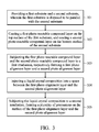
- Fig. 3 shows a flow chart illustrating a method for fabricating the liquid crystal module as shown in Fig. 1 ;
- Fig. 4 shows a scanning electron microscope (SEM) photograph of the photo-alignment layer having a plurality of protrusions thereon;
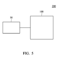
- Fig. 5 schematically shows a display system including the liquid crystal module of the invention.
- the invention provides a display device including a liquid crystal module, wherein the liquid crystal module includes novel photo-alignment layers.
- the photo-alignment layer of the invention has improved photostability and alignment ability.
- the invention also provides a method for fabricating a display device with reduced photo-alignment process time, thereby reducing cost and improving yield.
- an embodiment of the invention provides a liquid crystal module 100, wherein the liquid crystal module 100 includes a first substrate 12 and a second substrate 14.
- the first substrate 12 and second substrate 14 can be transparent substrates, such as a glass substrate.
- a first photo-alignment layer 16 is disposed on the top surface 11 of the first substrate 12, and a second photo-alignment layer 18 is disposed on the bottom surface 13 of the second substrate 14.
- the first photo-alignment layer 16 and the second photo-alignment layer 18 can be formed by subjecting a photo-degradable compound to a first irradiation, wherein the photo-degradable compound is a compound having a cyclobutane dianhydride moiety.
- the photo-degradable compound can be a compound having a repeat unit represented by wherein Ar is an aryl group (such as phenyl group, naphthyl group, diphenyl group, anthryl group, pyrenyl group, phenanthryl group, fluorine group, or multi-phenyl group).
- Ar is an aryl group (such as phenyl group, naphthyl group, diphenyl group, anthryl group, pyrenyl group, phenanthryl group, fluorine group, or multi-phenyl group).
- the photo-degradable compound can be a compound having a repeat unit represented by
- the first photo-alignment layer 16 and the second photo-alignment layer 18 can be formed by subjecting a photo-isomerizable compound to a first irradiation, wherein the photo-isomerizable compound can an azo compound.
- the photo-isomerizable compound is an azobenzene compound, such as a compound having
- Fig. 2 is a close-up diagram of region 2 of the liquid crystal module shown in Fig. 1 .
- the protrusions 22 are formed by polymerizing the non-polar monomers via a second irradiation, wherein the non-polar monomers can have two or three acrylate functional groups.
- the non-polar monomers can have a structure represented by or wherein R is methyl or ethyl.
- the non-polar monomers can have a structure represented by or wherein m and m' are independent integers from1 to 7, and n is an integer from 1 to 5.
- the protrusions 22 of the invention can increase the alignment ability of the first photo-alignment layer 16 and the second photo-alignment layer 18, thereby improving the anchoring strength between the photo-alignment film 16 (or 18) and the liquid crystal layer 20. Furthermore, the protrusions 22 of the invention can isolate the liquid crystal layer from the impurities produced in the photo-alignment process.
- an in-plane switching electrode 30 can be disposed on the top surface 11 of the first substrate 12. Namely, the in-plane switching electrode 30 can be disposed between the first photo-alignment layer 16 and the first substrate 12. According to another embodiment of the invention, the in-plane switching electrode 30 can be disposed between the second photo-alignment layer 18 and the second substrate 14.
- a liquid crystal layer 20 is disposed on the first photo-alignment layer 16 and the second photo-alignment layer 18.
- the liquid crystal module can be an in-plane switching liquid crystal module.
- Fig. 3 is a flow chart illustrating a method for fabricating the liquid crystal module 100 as shown in Fig. 1 .
- the method for fabricating the liquid crystal module can include the following steps:
- a first substrate and a second substrate are provided, wherein the first substrate is disposed to be parallel with the second substrate (step 101).
- a first photo-reactable compound layer is coated on the top surface of the first substrate, and a second photo-reactable compound layer is coated on the bottom surface of the second substrate (step 102).
- the photo-reactable compound can be a photo-degradable compound or a photo-isomerizable compound.
- the photo-degradable compound can be a compound having a cyclobutane dianhydride moiety.
- the photo-degradable compound can be a compound having a repeat unit represented by wherein Ar is an aryl group (such as phenyl group, naphthyl group, diphenyl group, anthryl group, pyrenyl group, phenanthryl group, fluorine group, or multi-phenyl group).
- Ar is an aryl group (such as phenyl group, naphthyl group, diphenyl group, anthryl group, pyrenyl group, phenanthryl group, fluorine group, or multi-phenyl group).
- the photo-degradable compound can be a compound having a repeat unit represented by
- the photo-isomerizable compound can an azo compound.
- the photo-isomerizable compound is an azobenzene compound, such as a compound having a structure represented by wherein R 1 is hydrogen, or C 1-6 alkyl.
- the first photo-reactable compound layer and the second photo-reactable compound layer are subjected to a first irradiation, respectively forming a first photo-alignment layer and a second photo-alignment layer (step 103).
- the first irradiation would be an ultraviolet light having a wavelength of 240-280nm (such as an ultraviolet light or a linear polarized light having a wavelength of 250nm).
- the first photo-reactable compound layer and the second photo-reactable compound layer are subjected to the first irradiation for a period of time of 1 to 100 seconds under an illuminance of 10-80 mW/cm 2 at a total exposure of 0.1-3J.
- the first irradiation would be an ultraviolet light or a linear polarized light having a wavelength of 365nm.
- the first photo-reactable compound layer and the second photo-reactable compound layer are subjected to the first irradiation for a period of time of 1 to 10 seconds under an illuminance of 10-80 mW/cm 2 at a total exposure of 0.01-0.8J.
- a liquid crystal composition is injected into the space between the first photo-alignment layer and the second photo-alignment layer (step 104), wherein the liquid crystal composition comprises a liquid crystal and non-polar monomers having two or three acrylate functional groups.
- the non-polar monomers can have a structure represented by or wherein R is methyl or ethyl.
- the non-polar monomers can have a structure represented by or wherein m and m' are independent integers from1 to 7, and n is an integer from 1 to 5.
- the non-polar monomer has a weight percentage of 0.05 to 3wt% (such as 0.3 wt %, 0.5 wt %, 1 wt %, 1.5 wt %, or 3 wt %), based on the weight of the liquid crystal composition.
- a non-polar monomer having an overly low weight percentage results the photo-alignment film having a poor alignment ability.
- a non-polar monomer having an overly high weight percentage results in a disordered alignment of the liquid crystal.
- the liquid crystal composition can be injected into the space between the first photo-alignment layer and the second photo-alignment layer by a one-drop filling process or a conventional liquid crystal injection process.
- the liquid crystal composition is subjected to a second irradiation (step 105), forcing the non-polar monomers of the liquid crystal composition to undergo polymerization and to adhere to the surfaces of the first photo-alignment layer and the second photo-alignment layer to form a plurality of protrusions.
- the second irradiation can be an ultraviolet light or a linear polarized light having a wavelength of 310 to 400nm.
- the first photo-reactable compound layer and the second photo-reactable compound layer are subjected to the first irradiation for a period of time of 50 seconds to 5 hours under an illuminance of 1-100mW/cm 2 at a total exposure of 0.5-100J.
- a first glass substrate and a second glass substrate were provided, wherein the first glass substrate was disposed to be parallel with the second glass substrate.
- a first photo-degradable compound layer was formed on the first glass substrate, and a second photo-degradable compound layer was formed on the second glass substrate predeterminedly, wherein the first photo-degradable compound layer was opposite to the second photo-degradable compound layer.
- the first photo-degradable compound layer and the second photo-degradable compound layer were made of a photo-degradable compound having a repeat unit represented by and the thickness of the first photo-degradable compound layer and the second photo-degradable compound layer can be 400-800mm.
- the first photo-degradable compound layer and the second photo-degradable compound layer were subjected to an ultraviolet light having a wavelength of 240 to 280nm, forming a first photo-alignment layer and a second photo-alignment layer respectively.
- the first photo-degradable compound layer and the second photo-degradable compound layer are subjected to the first irradiation for a period of time of 1 to 100 seconds under an illuminance of 10-80 mW/cm 2 at a total exposure of 0.5-3J.
- a liquid crystal composition was injected into the space between the first photo-alignment layer and the second photo-alignment layer by a one-drop filling process, forcing the liquid crystal composition to make direct contact with the surface of the first photo-alignment layer and the second photo-alignment layer.
- the liquid crystal composition included a liquid crystal (sold and manufactured by Merck) and a non-polar monomer having a structure represented by The non-polar monomer had a weight percentage of 1wt%, based on the weight of the liquid crystal composition.
- liquid crystal composition was subjected to an ultraviolet light having a wavelength of 310 to 380nm for 50 second to 5 hours under an illuminance of 1-100 mW/cm 2 at a total exposure of 0.5-100J, forming a plurality of protrusions on the surfaces of the first photo-alignment layer and the second photo-alignment layer.
- a first glass substrate and a second glass substrate were provided, wherein the first glass substrate was disposed to be parallel with the second glass substrate.
- a first photo-isomerizable compound layer was formed on the first glass substrate
- a second photo-isomerizable compound layer was formed on the second glass substrate predeterminedly, wherein the first photo-isomerizable compound layer was opposite to the second photo-isomerizable compound layer.
- the first photo-isomerizable compound layer and the second photo-isomerizable compound layer were made of a photo-isomerizable compound having a structure represented by and the thickness of the first photo-degradable compound layer and the second photo-degradable compound layer can be 400-800mm.
- the first photo-degradable compound layer and the second photo-degradable compound layer were subjected to an ultraviolet light having a wavelength of 365nm, forming a first photo-alignment layer and a second photo-alignment layer respectively.
- the first photo-isomerizable compound layer and the second photo-isomerizable compound layer are subjected to the first irradiation for a period of time of 10 to 500 seconds under an illuminance of 10-80 mW/cm 2 at a total exposure of 0.8-5J.
- a liquid crystal composition was injected into the space between the first photo-alignment layer and the second photo-alignment layer by a one-drop filling process, forcing the liquid crystal composition to make direct contact with the surface of the first photo-alignment layer and the second photo-alignment layer.
- the liquid crystal composition included a liquid crystal (sold and manufactured by Merck) and a non-polar monomer having a structure represented by The non-polar monomer had a weight percentage of 0.3wt%, based on the weight of the liquid crystal composition.
- liquid crystal composition was subjected to an ultraviolet light having a wavelength of 310 to 400nm for 100 to 1800 seconds under an illuminance of 5-10 mW/cm 2 at a total exposure of 0.5-18J, forming a plurality of protrusions on the surfaces of the first photo-alignment layer and the second photo-alignment layer.
- Fig. 4 is a scanning electron microscope (SEM) photograph of the photo-alignment layer having a plurality of protrusions thereon.
- the alignment film of the liquid crystal module of the invention exhibits improved photostability and alignment ability. Since the protrusions can increase the anchoring strength between the photo-alignment film and the liquid crystal layer, the period of time for irradiating the photo-reactable compound layer with an ultraviolet light can be reduced. Furthermore, the protrusions of the invention can isolate the liquid crystal layer from the impurities produced in the photo-alignment process.
- a display system 200 for displaying images including the liquid crystal module 100 is shown.
- the display system 200 can be an electrical device such as notebook computer, mobile phone, digital camera, personal data assistant (PDA), desktop computer, television, car display, or portable DVD player.
- the liquid crystal module 100 of the display system 200 can be further coupled to an input unit 50.
- the input unit 50 is operative to provide input to the liquid crystal module 100, such that the liquid crystal module 100 displays images.
Landscapes
- Physics & Mathematics (AREA)
- Nonlinear Science (AREA)
- General Physics & Mathematics (AREA)
- Chemical & Material Sciences (AREA)
- Crystallography & Structural Chemistry (AREA)
- Mathematical Physics (AREA)
- Optics & Photonics (AREA)
- Spectroscopy & Molecular Physics (AREA)
- Engineering & Computer Science (AREA)
- Manufacturing & Machinery (AREA)
- Liquid Crystal (AREA)
- Polarising Elements (AREA)
- Addition Polymer Or Copolymer, Post-Treatments, Or Chemical Modifications (AREA)
- Devices For Indicating Variable Information By Combining Individual Elements (AREA)
Abstract
Description
- This application is based upon and claims the benefit of priority from the prior Taiwan Patent Application No.
101103027, filed on Jan. 31, 2012 101109793, filed on Mar. 22, 2012 - The present invention relates to a display device, and in particular to a display device having a liquid crystal module.
- A liquid crystal display device is now being widely used attributed to its characteristics such as slim profile, light weight, and low electrical power consumption. The liquid crystal display device includes a pair of substrates and a liquid crystal layer interposed therebetween. Furthermore, the liquid crystal device provides display functionality by controlling the alignment direction of liquid crystal molecules contained in the liquid crystal layer by appropriately applying a voltage to electrodes arranged on liquid crystal layer side-surfaces of the substrates. The liquid crystal display device usually includes a liquid crystal alignment film (hereinafter, simply referred to as "alignment film") for controlling the alignment direction of the liquid crystal molecules, and the alignment film is arranged on the liquid crystal layer side-surface of the substrate.
- The liquid crystal alignment film is mainly made of polymer materials. The liquid crystal alignment film directs the alignment of liquid crystal molecules. When the liquid crystal molecules are moved by the influence of an electric field to display an image, the liquid crystal alignment film allows the liquid crystal molecules to be oriented in a predetermined direction. Generally, it is necessary to uniformly align the liquid crystal molecules in order to provide uniform luminance and a high contrast ratio to the liquid crystal device.
- The conventional method of aligning liquid crystal molecules includes coating a polymer film such as a polyimide on a substrate made of a material such as glass, and rubbing the surface of the substrate with a fiber such as nylon or polyester in a certain direction. However, the rubbing method may cause serious problems when fabricating a liquid crystal panel due to fine dust or electrostatic discharge (ESD) that may be generated while rubbing the polymer film with the fiber.
- In order to solve the problems associated with the rubbing method, a photo-radiation method has recently been researched to induce anisotropy to the polymer film by irradiating light on the membrane so as to align the liquid crystal molecules.
- The conventional photo-alignment process employs a polymer material having photo-curable functional groups. The polymer material having photo-curable functional groups is irradiated by a polarized light to undergo photo-isomerization, photo-crosslinking, or photo-degradation, thereby forming a photo-alignment film yielding anisotropy on the surface thereof. Therefore, the alignment of liquid crystal molecules alignment of liquid crystal can be achieved by means of the photo-alignment film.
- In order to ensure the reliability of the liquid crystal display device, suitable materials for the photo-alignment film should exhibit high photostability and thermal stability. However, since the photo-alignment film made of conventional polymer materials having photo-curable functional groups exhibits unstable alignment characteristic due to poor photostability and thermal stability, the liquid crystal display device cannot pass the production reliability test. Furthermore, the anchoring energy of alignment film fabricated by the photo-alignment process is less than that of alignment film fabricated by the rubbing-alignment process in general. Therefore, the liquid crystal display device employing the conventional photo-alignment film offers an inferior response speed and makes the generation of the image sticking more easily.
- Accordingly, a novel photo-alignment process, which forms an alignment film with improved stability and anchoring ability, is desired.
- An exemplary embodiment of the invention provides a display device. The display device includes a liquid crystal module, wherein the display device includes: a first substrate and a second substrate, wherein the first substrate has a top surface and the second substrate has a bottom surface, and wherein the top surface of the first substrate is disposed opposite to the bottom surface of the second substrate; a first photo-alignment layer disposed on the top surface of the first substrate, and a second photo-alignment layer disposed on the bottom surface of the second substrate, wherein the first and second photo-alignment layers comprise a plurality of protrusions, and wherein the protrusions are formed by polymerizing non-polar monomers having two or three acrylate functional groups; and a liquid crystal layer disposed between the first and second photo-alignment layers.
- Another exemplary embodiment of the invention provides a method for fabricating the liquid crystal module of the display device, including: providing a first substrate and a second substrate, wherein the first substrate has a top surface and the second substrate has a bottom surface; forming a first photo-reactable compound layer on the top surface of the first substrate, and forming a second photo-reactable compound layer on the bottom surface of the second substrate; subjecting the first photo-reactable compound layer and the second photo-reactable compound layer to a first irradiation, respectively forming a first photo-alignment layer and a second photo-alignment layer; aligning and combining the first substrate with the second substrate, wherein the top surface of the first substrate is disposed opposite to the bottom surface of the second substrate; providing a liquid crystal composition into the space between the first photo-alignment layer and the second photo-alignment layer, wherein the liquid crystal composition comprises a liquid crystal and non-polar monomers having two or three acrylate functional groups; and subjecting the liquid crystal composition to a second irradiation, forming a plurality of protrusions on the surfaces of the first photo-alignment layer and the second photo-alignment layer, wherein the protrusions are formed by polymerizing the non-polar monomers.
- A detailed description is given in the following embodiments with reference to the accompanying drawings.
- The disclosure can be more fully understood by reading the subsequent detailed description and examples with references made to the accompanying drawings, wherein:
-
Fig. 1 shows a schematic cross section of the liquid crystal module according to an embodiment of the invention; -
Fig. 2 shows a close-up diagram ofregion 2 of the liquid crystal module shown inFig. 1 ; -
Fig. 3 shows a flow chart illustrating a method for fabricating the liquid crystal module as shown inFig. 1 ; -
Fig. 4 shows a scanning electron microscope (SEM) photograph of the photo-alignment layer having a plurality of protrusions thereon; and -
Fig. 5 schematically shows a display system including the liquid crystal module of the invention. - Accordingly, the invention provides a display device including a liquid crystal module, wherein the liquid crystal module includes novel photo-alignment layers. In comparison with the convention photo-alignment layer, the photo-alignment layer of the invention has improved photostability and alignment ability. The invention also provides a method for fabricating a display device with reduced photo-alignment process time, thereby reducing cost and improving yield.
- As shown in
Fig. 1 , an embodiment of the invention provides aliquid crystal module 100, wherein theliquid crystal module 100 includes afirst substrate 12 and asecond substrate 14. Thefirst substrate 12 andsecond substrate 14 can be transparent substrates, such as a glass substrate. A first photo-alignment layer 16 is disposed on thetop surface 11 of thefirst substrate 12, and a second photo-alignment layer 18 is disposed on thebottom surface 13 of thesecond substrate 14. The first photo-alignment layer 16 and the second photo-alignment layer 18 can be formed by subjecting a photo-degradable compound to a first irradiation, wherein the photo-degradable compound is a compound having a cyclobutane dianhydride moiety. For example, the photo-degradable compound can be a compound having a repeat unit represented by

alignment layer 16 and the second photo-alignment layer 18 can be formed by subjecting a photo-isomerizable compound to a first irradiation, wherein the photo-isomerizable compound can an azo compound. For example, the photo-isomerizable compound is an azobenzene compound, such as a compound having a structure represented by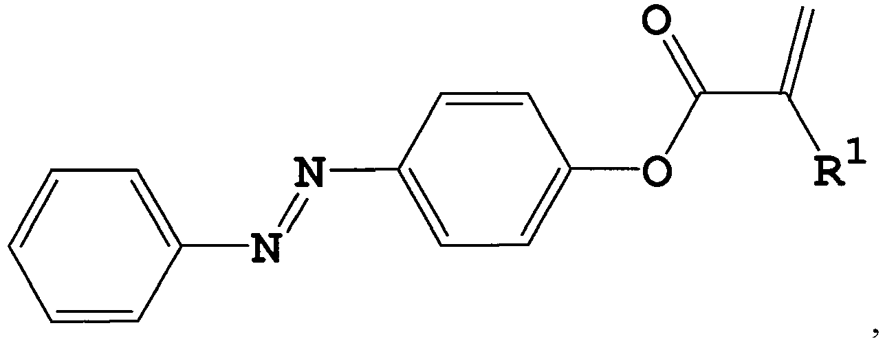
-
Fig. 2 is a close-up diagram ofregion 2 of the liquid crystal module shown inFig. 1 . It should be noted that there are a plurality ofprotrusions 22 disposed on thetop surface 15 of the first photo-alignment layer 16 and thebottom surface 17 of the second photo-alignment layer 18, wherein the protrusions have a height of less than or equal to 20nm and a width of less than or equal to 200nm. Particularly, theprotrusions 22 are formed by polymerizing the non-polar monomers via a second irradiation, wherein the non-polar monomers can have two or three acrylate functional groups. For example, the non-polar monomers can have a structure represented by


- The
protrusions 22 of the invention can increase the alignment ability of the first photo-alignment layer 16 and the second photo-alignment layer 18, thereby improving the anchoring strength between the photo-alignment film 16 (or 18) and theliquid crystal layer 20. Furthermore, theprotrusions 22 of the invention can isolate the liquid crystal layer from the impurities produced in the photo-alignment process. According to some embodiments of the invention, an in-plane switching electrode 30 can be disposed on thetop surface 11 of thefirst substrate 12. Namely, the in-plane switching electrode 30 can be disposed between the first photo-alignment layer 16 and thefirst substrate 12. According to another embodiment of the invention, the in-plane switching electrode 30 can be disposed between the second photo-alignment layer 18 and thesecond substrate 14. - Still referring to
Fig. 1 , aliquid crystal layer 20 is disposed on the first photo-alignment layer 16 and the second photo-alignment layer 18. According to an embodiment of the invention, the liquid crystal module can be an in-plane switching liquid crystal module. -
Fig. 3 is a flow chart illustrating a method for fabricating theliquid crystal module 100 as shown inFig. 1 . The method for fabricating the liquid crystal module can include the following steps: - First, a first substrate and a second substrate are provided, wherein the first substrate is disposed to be parallel with the second substrate (step 101). Next, a first photo-reactable compound layer is coated on the top surface of the first substrate, and a second photo-reactable compound layer is coated on the bottom surface of the second substrate (step 102). The photo-reactable compound can be a photo-degradable compound or a photo-isomerizable compound. The photo-degradable compound can be a compound having a cyclobutane dianhydride moiety. For example, the photo-degradable compound can be a compound having a repeat unit represented by


- Next, after the formation of the photo-reactable compound layer, aligning and combining the first substrate with the second substrate, wherein the top surface of the first substrate is facing and joined with the bottom surface of the second substrate, the first photo-reactable compound layer and the second photo-reactable compound layer are subjected to a first irradiation, respectively forming a first photo-alignment layer and a second photo-alignment layer (step 103). It should be noted that, if the photo-reactable compound is a photo-degradable compound, the first irradiation would be an ultraviolet light having a wavelength of 240-280nm (such as an ultraviolet light or a linear polarized light having a wavelength of 250nm). In this state, the first photo-reactable compound layer and the second photo-reactable compound layer are subjected to the first irradiation for a period of time of 1 to 100 seconds under an illuminance of 10-80 mW/cm2 at a total exposure of 0.1-3J.
- If the photo-reactable compound is a photo-isomerizable compound, the first irradiation would be an ultraviolet light or a linear polarized light having a wavelength of 365nm. In this case, the first photo-reactable compound layer and the second photo-reactable compound layer are subjected to the first irradiation for a period of time of 1 to 10 seconds under an illuminance of 10-80 mW/cm2 at a total exposure of 0.01-0.8J.
- After formation of the first photo-alignment layer and the second photo-alignment layer, a liquid crystal composition is injected into the space between the first photo-alignment layer and the second photo-alignment layer (step 104), wherein the liquid crystal composition comprises a liquid crystal and non-polar monomers having two or three acrylate functional groups. For example, the non-polar monomers can have a structure represented by


- A non-polar monomer having an overly low weight percentage (less than 0.05wt%) results the photo-alignment film having a poor alignment ability. On the other hand, a non-polar monomer having an overly high weight percentage (more than 3wt%) results in a disordered alignment of the liquid crystal.
- The liquid crystal composition can be injected into the space between the first photo-alignment layer and the second photo-alignment layer by a one-drop filling process or a conventional liquid crystal injection process. Finally, after injection of the liquid crystal composition, the liquid crystal composition is subjected to a second irradiation (step 105), forcing the non-polar monomers of the liquid crystal composition to undergo polymerization and to adhere to the surfaces of the first photo-alignment layer and the second photo-alignment layer to form a plurality of protrusions. Thus, the fabrication of the liquid crystal module is completed. The second irradiation can be an ultraviolet light or a linear polarized light having a wavelength of 310 to 400nm. In this state, the first photo-reactable compound layer and the second photo-reactable compound layer are subjected to the first irradiation for a period of time of 50 seconds to 5 hours under an illuminance of 1-100mW/cm2 at a total exposure of 0.5-100J.
- The following examples are intended to illustrate the invention more fully without limiting its scope, since numerous modifications and variations will be apparent to those skilled in this art.
- Example 1:
- First, a first glass substrate and a second glass substrate were provided, wherein the first glass substrate was disposed to be parallel with the second glass substrate. In particular, a first photo-degradable compound layer was formed on the first glass substrate, and a second photo-degradable compound layer was formed on the second glass substrate predeterminedly, wherein the first photo-degradable compound layer was opposite to the second photo-degradable compound layer. The first photo-degradable compound layer and the second photo-degradable compound layer were made of a photo-degradable compound having a repeat unit represented by


- Example 2:
- First, a first glass substrate and a second glass substrate were provided, wherein the first glass substrate was disposed to be parallel with the second glass substrate. Particularly, a first photo-isomerizable compound layer was formed on the first glass substrate, and a second photo-isomerizable compound layer was formed on the second glass substrate predeterminedly, wherein the first photo-isomerizable compound layer was opposite to the second photo-isomerizable compound layer. The first photo-isomerizable compound layer and the second photo-isomerizable compound layer were made of a photo-isomerizable compound having a structure represented by


Fig. 4 is a scanning electron microscope (SEM) photograph of the photo-alignment layer having a plurality of protrusions thereon. - Accordingly, due to the specific photo-reactable compound and the protrusions formed on the surface of the protrusions, the alignment film of the liquid crystal module of the invention exhibits improved photostability and alignment ability. Since the protrusions can increase the anchoring strength between the photo-alignment film and the liquid crystal layer, the period of time for irradiating the photo-reactable compound layer with an ultraviolet light can be reduced. Furthermore, the protrusions of the invention can isolate the liquid crystal layer from the impurities produced in the photo-alignment process.
- Referring to
Fig. 5 , adisplay system 200 for displaying images including theliquid crystal module 100 according to an embodiment of the invention is shown. Thedisplay system 200 can be an electrical device such as notebook computer, mobile phone, digital camera, personal data assistant (PDA), desktop computer, television, car display, or portable DVD player. Theliquid crystal module 100 of thedisplay system 200 can be further coupled to aninput unit 50. Theinput unit 50 is operative to provide input to theliquid crystal module 100, such that theliquid crystal module 100 displays images. - While the disclosure has been described by way of example and in terms of the preferred embodiments, it is to be understood that the disclosure is not limited to the disclosed embodiments. On the contrary, it is intended to cover various modifications and similar arrangements (as would be apparent to those skilled in the art). Therefore, the scope of the appended claims should be accorded the broadest interpretation so as to encompass all such modifications and similar arrangements.
Claims (18)
- A display device, comprising:a liquid crystal module, comprising:a first substrate and a second substrate, wherein the first substrate has a top surface and the second substrate has a bottom surface, and wherein the top surface of the first substrate is disposed opposite to the bottom surface of the second substrate;a first photo-alignment layer disposed on the top surface of the first substrate, and a second photo-alignment layer disposed on the bottom surface of the second substrate, wherein the first and second photo-alignment layers comprise a plurality of protrusions, and wherein the protrusions are formed by polymerizing non-polar monomers having two or three acrylate functional groups; anda liquid crystal layer disposed between the first and second photo-alignment layers.
- The display device as claimed in claim 1, wherein the non-polar monomers have a structure represented by


- The display device as claimed in claim 1, wherein the non-polar monomers have a structure represented by


- The display device as claimed in any of the preceding claims, wherein the first photo-alignment layer and the second photo-alignment layer are formed by subjecting a photo-degradable compound to a first irradiation.
- The display device as claimed in claim 4, wherein the photo-degradable compound is a compound having a repeat unit
represented by
wherein the photo-degradable compound is a compound having a repeat unit represented by
- The display device as claimed in any of claims 1 to 3, wherein the first photo-alignment layer and the second photo-alignment layer are formed by subjecting a photo-isomerizable compound to a first irradiation.
- The display device as claimed in claim 6, wherein the photo-isomerizable compound is a compound having a structure represented by

- The display device as claimed in any of the preceding claims, wherein the protrusions are formed by subjecting the non-polar monomers to a second irradiation and the protrusions have a height of less than or equal to 20nm and a width of less than or equal to 200nm.
- The display device as claimed in any of the preceding claims, wherein the liquid crystal module is an in-plane switching liquid crystal module and is further comprising an in-plane switching electrode disposed on the top surface of the first substrate and disposed on the bottom surface of the second substrate.
- A method for fabricating a display device, in particular a display device according to any of the preceding claims, comprising:providing a first substrate and a second substrate, wherein the first substrate has a top surface and the second substrate has a bottom surface;forming a first photo-reactable compound layer on the top surface of the first substrate, and forming a second photo-reactable compound layer on the bottom surface of the second substrate;subjecting the first photo-reactable compound layer and the second photo-reactable compound layer to a first irradiation, respectively forming a first photo-alignment layer and a second photo-alignment layer;aligning and combining the first substrate with the second substrate, wherein the top surface of the first substrate is disposed opposite to the bottom surface of the second substrate;providing a liquid crystal composition into the space between the first photo-alignment layer and the second photo-alignment layer, wherein the liquid crystal composition comprises a liquid crystal and non-polar monomers having two or three acrylate functional groups; andsubjecting the liquid crystal composition to a second irradiation, forming a plurality of protrusions on the surfaces of the first photo-alignment layer and the second photo-alignment layer, wherein the protrusions are formed by polymerizing the non-polar monomers.
- The method as claimed in claim 10, wherein the first photo-reactable compound layer and the second photo-reactable compound layer comprise a photo-degradable compound.
- The method as claimed in claim 11,
wherein the photo-degradable compound is a compound having a repeat unit represented by
wherein the photo-degradable compound is a compound having a repeat unit represented by
- The method as claimed in claim 11 or 12, wherein the first irradiation is an ultraviolet light having a wavelength of 240-280nm and the first photo-reactable compound layer and the second photo-reactable compound layer are subjected to the first irradiation for a period of time of 1 to 100 seconds.
- The method as claimed in any of claims 10 to 13, wherein the first photo-reactable compound layer and the second photo-reactable compound layer comprise a photo-isomerizable compound.
- The method as claimed in claim 14, wherein the photo-isomerizable compound is a compound having a structure represented by

- The method as claimed in claim 14 or 15, wherein the first irradiation is an ultraviolet light having a wavelength of 365nm and the first photo-reactable compound layer and the second photo-reactable compound layer are subjected to the first irradiation for a period of time of 1 to 10 seconds.
- The method as claimed in any of claims 10 to 16, wherein the weight percentage of the non-polar monomers is from 0.05 to 3wt%, based on the weight of the liquid crystal composition.
- The method as claimed in claim 14, wherein the second irradiation is an ultraviolet light having a wavelength of 310-400nm and the liquid crystal composition is subjected to a second irradiation for a period of time of 50 second to 5 hours.
Applications Claiming Priority (2)
| Application Number | Priority Date | Filing Date | Title |
|---|---|---|---|
| TW101103027A TWI498646B (en) | 2012-01-31 | 2012-01-31 | Image display system employing a liquid crystal device and method for fabricating the liquid crystal device |
| TW101109793A TWI490263B (en) | 2012-03-22 | 2012-03-22 | Image display device employing a liquid crystal module and method for fabricating the liquid crystal module |
Publications (2)
| Publication Number | Publication Date |
|---|---|
| EP2624047A2 true EP2624047A2 (en) | 2013-08-07 |
| EP2624047A3 EP2624047A3 (en) | 2013-09-25 |
Family
ID=47623941
Family Applications (1)
| Application Number | Title | Priority Date | Filing Date |
|---|---|---|---|
| EP20130152528 Withdrawn EP2624047A3 (en) | 2012-01-31 | 2013-01-24 | Display Device And Method For Fabricating The Same |
Country Status (3)
| Country | Link |
|---|---|
| US (1) | US20130194533A1 (en) |
| EP (1) | EP2624047A3 (en) |
| JP (1) | JP2013156634A (en) |
Families Citing this family (2)
| Publication number | Priority date | Publication date | Assignee | Title |
|---|---|---|---|---|
| KR20180019794A (en) * | 2016-08-16 | 2018-02-27 | 삼성디스플레이 주식회사 | Liquid crystal display apparatus and method of manufacturing the same |
| CN107517338B (en) * | 2017-09-05 | 2020-06-02 | 维沃移动通信有限公司 | Electronic device back shell, electronic device and shooting method |
Citations (2)
| Publication number | Priority date | Publication date | Assignee | Title |
|---|---|---|---|---|
| US20100208183A1 (en) * | 2008-09-17 | 2010-08-19 | Kim Jae-Hoon | Alignment material, alignment layer, liquid crystal display device and manufacturing method thereof |
| US20110115999A1 (en) * | 2009-11-13 | 2011-05-19 | Hitachi Displays, Ltd. | Liquid crystal display device and manufacturing method thereof |
Family Cites Families (2)
| Publication number | Priority date | Publication date | Assignee | Title |
|---|---|---|---|---|
| TWI281063B (en) * | 2005-08-16 | 2007-05-11 | Chi Mei Optoelectronics Corp | Liquid crystal display panel and manufacturing method for the same |
| KR101499238B1 (en) * | 2008-08-07 | 2015-03-05 | 삼성디스플레이 주식회사 | Liquid crystal display |
-
2013
- 2013-01-24 EP EP20130152528 patent/EP2624047A3/en not_active Withdrawn
- 2013-01-30 JP JP2013015375A patent/JP2013156634A/en active Pending
- 2013-01-30 US US13/753,784 patent/US20130194533A1/en not_active Abandoned
Patent Citations (2)
| Publication number | Priority date | Publication date | Assignee | Title |
|---|---|---|---|---|
| US20100208183A1 (en) * | 2008-09-17 | 2010-08-19 | Kim Jae-Hoon | Alignment material, alignment layer, liquid crystal display device and manufacturing method thereof |
| US20110115999A1 (en) * | 2009-11-13 | 2011-05-19 | Hitachi Displays, Ltd. | Liquid crystal display device and manufacturing method thereof |
Also Published As
| Publication number | Publication date |
|---|---|
| US20130194533A1 (en) | 2013-08-01 |
| EP2624047A3 (en) | 2013-09-25 |
| JP2013156634A (en) | 2013-08-15 |
Similar Documents
| Publication | Publication Date | Title |
|---|---|---|
| CN102362218B (en) | Liquid crystal display and manufacture method thereof | |
| JP5333693B1 (en) | Liquid crystal display element and manufacturing method thereof | |
| CN107418598B (en) | Liquid crystal material, liquid crystal display panel and its manufacturing method | |
| US9261733B2 (en) | Liquid crystal display device and method for producing the same | |
| EP2701003B1 (en) | Liquid crystal display element | |
| CN105733557A (en) | Ligand modification quantum dot material, producing method of liquid crystal display panel and liquid crystal display panel | |
| JP2002341358A (en) | Liquid crystal display panel manufacturing method | |
| CN105273725B (en) | Aligning agent for liquid crystal, liquid crystal orientation film and liquid crystal display element | |
| CN104662469B (en) | Liquid crystal disply device and its preparation method | |
| KR20120061427A (en) | UV-Curable Composition for Liquid Crystal Display and Liquid Crystal Display using the same | |
| US10899966B2 (en) | Self-oriented material, self-oriented liquid crystal material and manufacturing method of liquid crystal panel | |
| US20130194533A1 (en) | Display device and method for fabricating the same | |
| WO2014034517A1 (en) | Liquid crystal display device and method for manufacturing same | |
| US20160304782A1 (en) | Liquid crystal display element and method for producing same | |
| CN111198452A (en) | Liquid crystal display device | |
| CN104099106A (en) | Liquid Crystal Aligning Agent And Forming Method Thereof, Liquid Crystal Alignment Film And Forming Method Thereof, Phase Difference Film And Manufacturing Method Thereof, And Liquid Crystal Display Device And Manufacturing Method Thereof | |
| CN111198459A (en) | Liquid crystal display device having a plurality of pixel electrodes | |
| CN103226262B (en) | The manufacture method of image display system and liquid crystal indicator | |
| TW201835163A (en) | Liquid crystal element and method for producing same | |
| TWI228194B (en) | Optical compensated bend nematic liquid crystal display panel | |
| WO2014075334A1 (en) | Liquid crystal additive and liquid crystal composition and liquid crystal panel thereof | |
| CN104714337A (en) | Liquid crystal display panel and liquid crystal display device | |
| CN106842714A (en) | Display base plate, display panel and display device | |
| CN103323977A (en) | Image display device provided with liquid crystal display module and manufacturing method of liquid crystal display module | |
| TWI498646B (en) | Image display system employing a liquid crystal device and method for fabricating the liquid crystal device |
Legal Events
| Date | Code | Title | Description |
|---|---|---|---|
| PUAI | Public reference made under article 153(3) epc to a published international application that has entered the european phase |
Free format text: ORIGINAL CODE: 0009012 |
|
| AK | Designated contracting states |
Kind code of ref document: A2 Designated state(s): AL AT BE BG CH CY CZ DE DK EE ES FI FR GB GR HR HU IE IS IT LI LT LU LV MC MK MT NL NO PL PT RO RS SE SI SK SM TR |
|
| AX | Request for extension of the european patent |
Extension state: BA ME |
|
| PUAL | Search report despatched |
Free format text: ORIGINAL CODE: 0009013 |
|
| AK | Designated contracting states |
Kind code of ref document: A3 Designated state(s): AL AT BE BG CH CY CZ DE DK EE ES FI FR GB GR HR HU IE IS IT LI LT LU LV MC MK MT NL NO PL PT RO RS SE SI SK SM TR |
|
| AX | Request for extension of the european patent |
Extension state: BA ME |
|
| RIC1 | Information provided on ipc code assigned before grant |
Ipc: G02F 1/1337 20060101AFI20130816BHEP |
|
| 17P | Request for examination filed |
Effective date: 20140325 |
|
| RBV | Designated contracting states (corrected) |
Designated state(s): AL AT BE BG CH CY CZ DE DK EE ES FI FR GB GR HR HU IE IS IT LI LT LU LV MC MK MT NL NO PL PT RO RS SE SI SK SM TR |
|
| STAA | Information on the status of an ep patent application or granted ep patent |
Free format text: STATUS: EXAMINATION IS IN PROGRESS |
|
| 17Q | First examination report despatched |
Effective date: 20170130 |
|
| STAA | Information on the status of an ep patent application or granted ep patent |
Free format text: STATUS: THE APPLICATION IS DEEMED TO BE WITHDRAWN |
|
| 18D | Application deemed to be withdrawn |
Effective date: 20170610 |