EP2619762B1 - Replaceable, precise-tracking reference lines for memory products - Google Patents
Replaceable, precise-tracking reference lines for memory products Download PDFInfo
- Publication number
- EP2619762B1 EP2619762B1 EP11827099.0A EP11827099A EP2619762B1 EP 2619762 B1 EP2619762 B1 EP 2619762B1 EP 11827099 A EP11827099 A EP 11827099A EP 2619762 B1 EP2619762 B1 EP 2619762B1
- Authority
- EP
- European Patent Office
- Prior art keywords
- word lines
- pair
- section
- sections
- reference word
- Prior art date
- Legal status (The legal status is an assumption and is not a legal conclusion. Google has not performed a legal analysis and makes no representation as to the accuracy of the status listed.)
- Active
Links
Images



Classifications
-
- G—PHYSICS
- G11—INFORMATION STORAGE
- G11C—STATIC STORES
- G11C7/00—Arrangements for writing information into, or reading information out from, a digital store
- G11C7/18—Bit line organisation; Bit line lay-out
-
- G—PHYSICS
- G11—INFORMATION STORAGE
- G11C—STATIC STORES
- G11C13/00—Digital stores characterised by the use of storage elements not covered by groups G11C11/00, G11C23/00, or G11C25/00
- G11C13/0002—Digital stores characterised by the use of storage elements not covered by groups G11C11/00, G11C23/00, or G11C25/00 using resistive RAM [RRAM] elements
- G11C13/0004—Digital stores characterised by the use of storage elements not covered by groups G11C11/00, G11C23/00, or G11C25/00 using resistive RAM [RRAM] elements comprising amorphous/crystalline phase transition cells
-
- G—PHYSICS
- G11—INFORMATION STORAGE
- G11C—STATIC STORES
- G11C13/00—Digital stores characterised by the use of storage elements not covered by groups G11C11/00, G11C23/00, or G11C25/00
- G11C13/0002—Digital stores characterised by the use of storage elements not covered by groups G11C11/00, G11C23/00, or G11C25/00 using resistive RAM [RRAM] elements
- G11C13/0021—Auxiliary circuits
- G11C13/004—Reading or sensing circuits or methods
-
- G—PHYSICS
- G11—INFORMATION STORAGE
- G11C—STATIC STORES
- G11C7/00—Arrangements for writing information into, or reading information out from, a digital store
- G11C7/06—Sense amplifiers; Associated circuits, e.g. timing or triggering circuits
-
- G—PHYSICS
- G11—INFORMATION STORAGE
- G11C—STATIC STORES
- G11C8/00—Arrangements for selecting an address in a digital store
- G11C8/14—Word line organisation; Word line lay-out
-
- G—PHYSICS
- G11—INFORMATION STORAGE
- G11C—STATIC STORES
- G11C13/00—Digital stores characterised by the use of storage elements not covered by groups G11C11/00, G11C23/00, or G11C25/00
- G11C13/0002—Digital stores characterised by the use of storage elements not covered by groups G11C11/00, G11C23/00, or G11C25/00 using resistive RAM [RRAM] elements
- G11C13/0021—Auxiliary circuits
- G11C13/004—Reading or sensing circuits or methods
- G11C2013/0054—Read is performed on a reference element, e.g. cell, and the reference sensed value is used to compare the sensed value of the selected cell
-
- G—PHYSICS
- G11—INFORMATION STORAGE
- G11C—STATIC STORES
- G11C2211/00—Indexing scheme relating to digital stores characterized by the use of particular electric or magnetic storage elements; Storage elements therefor
- G11C2211/56—Indexing scheme relating to G11C11/56 and sub-groups for features not covered by these groups
- G11C2211/563—Multilevel memory reading aspects
- G11C2211/5634—Reference cells
Definitions
- This invention relates generally to memory products and relates more specifically to reference line structures associated with a reading cell.
- a sense amplifier compares a reference signal, which is middle point between stored 1 and 0 signals, with a stored signal.
- Figs.1 a + b prior art show two examples used in conventional memories. For memories, in which an adjacent bit line to the accessed bit line can be used to put the reference signal, a pair of reference word lines is generally exploited.
- a folded bit line memory array is the typical example, and Fig. 1a prior art shows its scheme. For simplicity, one reference word line shown here is connected to one reference cell, but it is assumed that a middle point of stored 1 and 0 signals appears on the bit line when this reference word line is selected.
- multiplexer Mux 2 selects these two bit lines to connect to a sense amplifier.
- the sense amplifier compares two signals to judge read data as either 1 or 0.
- an upper reference of the reference word line pair is selected.
- the second example shown in Fig.1 (B) is based on a reference bit line. It is assumed that the middle point of stored 1 and 0 signals appears on the reference bit line. The array block shares this reference bit line, which is always selected to provide the reference signal to the sense amplifier. Depending on the column address, Mux selects accessed bit line to connect as the input to the sense amplifier
- the purpose of this invention is to realize reference lines for reliable sensing operations and to provide a means for yield enhancement.
- U. S. Patent Publication proposes a semiconductor integrated circuit including: a current difference sense type of a sense amplifier including: an input line connected to memory cells as a target to be read, a reference line connected to reference cells, and a first pre-charge circuit configured to pre-charge the input line and the reference line; a second pre-charge circuit configured to perform pre-charging of the input line and pre-charging of the reference line; and a control circuit configured to control the second pre-charge circuit so that the second pre-charge circuit may perform both the pre-charging of the input line and the pre-charging of the reference line independently of each other, and start both the pre-charging of the input line and the pre-charging of the reference line earlier than pre-charging by the first pre-charge circuit.
- a current difference sense type of a sense amplifier including: an input line connected to memory cells as a target to be read, a reference line connected to reference cells, and a first pre-charge circuit configured to pre-charge the input line and the reference line; a second pre-charge circuit
- U. S. Patent Publication ( US 2009/0067274 to Beer ) discloses a memory device comprising a memory cell and an evaluation circuit, the memory cell being coupled with the evaluation circuit via a bit line.
- the memory device further comprises a reference line coupled with the evaluation circuit, the evaluation circuit being designed for amplifying a difference between electric potentials of the bit line and the reference line.
- Inputs of the evaluation circuit are directly connected to the bit line.
- Outputs of the evaluation circuit are coupled to the bit line via a switch.
- U. S. Patent discloses a reading circuit, for reading data from one memory cell of a plurality of memory cells, includes a plurality of division sensing circuits each connected to the one memory cell via a sensing line corresponding thereto among a plurality of sensing lines; and a current-voltage conversion circuit for converting a current flowing through each sensing line into a sensing voltage representing a potential of the corresponding sensing line.
- Each division sensing circuit includes a current load circuit for supplying a current to the one memory cell via a corresponding sensing line, and a sense amplifier for sensing a potential difference between the corresponding sensing line and a corresponding reference line of a plurality of reference lines.
- the current load circuit included in at least one division sensing circuit has a current supply capability different from that of the current load circuit included in another division sensing circuits.
- ReRAM Resistance based Random Access Memory
- a current reference circuit including at least three ReRAM reference cells coupled in parallel with one another and configured to provide a reference current to respective ReRAM sense amplifier circuits.
- US-B-6,438,053 discloses a ferroelectric random access memory wherein the array comprises redundant word lines for selectively replacing one of the word lines or for replacing one of the reference word lines.
- the invention is defined by independent method claim 1 and independent apparatus claim 4.
- a principal object of the present invention is to achieve methods and systems for reliable sensing operations for semiconductor memories.
- a further object of the invention is to achieve yield enhancements for semiconductor memories.
- a further object of the present invention is to increase the number of active word reference lines.
- a further object of the present invention is to increase the number of active bit reference lines.
- a further object of the present invention is to increase the number of spare bit reference lines.
- a further object of the present invention is to increase the number of spare word reference lines.
- Another object of the invention is to divide a memory array into sections having each own word reference lines.
- Another object of the invention is to divide a memory array into sections having each own word reference lines and word spare lines.
- a further object of the invention is to divide a memory array into segments having each own bit reference lines and bit spare lines.
- MRAM Magneto-resistive Random Access Memory
- PCM phase change memory
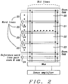
- Fig. 2 shows an example applying reference word lines to the conventional scheme, shown in Fig. 1a prior art.
- multiple reference word lines are provided.
- Fig. 2 shows that the array is divided into four sections 20 - 23, and each one has a reference word line pair 24.
- Word lines 25 in each one of four sections 20 - 23 use the reference word line pair 24 in that section.
- the distance between an accessed line and the correspondent reference line is reduced, and hence the parasitic parameter tracking capability is enhanced significantly.
- Albeit Fig. 2 shows four sections only, the example is of course not limited to four sections only. Any multiple numbers of sections are applicable depending on array situations.
- the location of the reference word line pair also does not have to be at the bottom of the section. It can be at top or middle of each section, or any arbitrary place regarding to the optimization.
- a defect When a defect hits a word line, memory chips generally replace it by a redundancy word line. Thus, there is no yield loss even if memory products have some defective word lines.
- the reference word lines are identical to word lines, and they are also subject to defects. However, if a defect hits any one of a reference word line, the memory chip affected cannot be saved, because all cells on word lines that share the defective reference word line cannot be read correctly.
- the second example shown in Fig. 3 , illustrates spare pairs 30 of reference word lines deployed in Fig. 3 for a non-limiting example again in four sections 20 - 23.
- the spare reference word lines 30 in each section 20 - 23 can replace defective reference word lines in the same way as redundancy word lines.
- the spare reference word line pair is placed above the reference word line pair in the figure.
- its location is also not limited here only. To avoid cluster fail by large defects, placing the spare at the other end of the section than the "regular" reference word lines could be better, but any other location can be applicable.
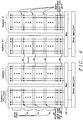
- FIG. 4 An embodiment of the present invention is shown in Fig. 4 .
- the embodiment comprises the application of the same multiple and spare reference word line pairs as shown in Fig. 3 but to a different array structure rather than the folded bit line scheme. It is based on a segmented array structure.
- the top word line in the top section 42 of segment 0 is accessed, one of the reference word line pairs 40 of the top section of segment 1 is selected.
- read bit line in segment 0 and the referenced bit line in segment 1 are connected to the sense amplifier through multiplexer Mux 46.
- Fig. 5 shows an example for using reference bit lines. As shown in Fig. 5 each segment of segments 0 - N has reference bit lines and spare reference bit lines at its both end, but it should be noted that locations of the reference bit line and the spare bit reference lines are arbitrary and could be deployed at any suitable location.
- bit line direction more than one reference bit line can be allocated to each section, if there is a relative high probability of bit line failures.
- Fig. 5 could have alternatively only reference bit lines for each segment without deploying additional spare reference bit lines. In case there is a process defect pattern showing defects in both bit line and word line direction it might become necessary placing both spare reference bit lines and spare reference word lines in order to achieve a reasonable yield.
- Fig. 6 illustrates a simplified flowchart to achieve reliable sensing operations for semiconductor memories and to enhance the yield of the semiconductor memories.
- Step 60 of the method of Fig. 6 illustrates the provision of a semiconductor memory array.
- Step 61 describes dividing the semiconductor array into multiple parts. As described above these parts could be sections or segments or both and step 62 illustrates deploying in each of said parts reference lines. These reference lines could comprise bit reference lines, potentially spare bit reference lines, or word reference lines, and potentially spare word reference lines.
Landscapes
- Engineering & Computer Science (AREA)
- Microelectronics & Electronic Packaging (AREA)
- Chemical & Material Sciences (AREA)
- Crystallography & Structural Chemistry (AREA)
- For Increasing The Reliability Of Semiconductor Memories (AREA)
Description
- This invention relates generally to memory products and relates more specifically to reference line structures associated with a reading cell.
- In a read operation of memory chips, a sense amplifier compares a reference signal, which is middle point between stored 1 and 0 signals, with a stored signal. There are various ways to provide such reference signals.
Figs.1 a + b prior art show two examples used in conventional memories. For memories, in which an adjacent bit line to the accessed bit line can be used to put the reference signal, a pair of reference word lines is generally exploited. A folded bit line memory array is the typical example, andFig. 1a prior art shows its scheme. For simplicity, one reference word line shown here is connected to one reference cell, but it is assumed that a middle point of stored 1 and 0 signals appears on the bit line when this reference word line is selected. When an even word line is accessed and the cell shown by a red dot is turned on. The stored signal, thus, appears on the bit line. Simultaneously, a lower one of the reference word line pair is tuned on to bring the reference signal on the adjacent bit line. According to the column address, multiplexer Mux 2 selects these two bit lines to connect to a sense amplifier. The sense amplifier compares two signals to judge read data as either 1 or 0. When an odd word line is accessed, an upper reference of the reference word line pair is selected. Thus, one pair of bit lines, which are adjacent each other, is always selected as inputs to the same amplifier that is shared in this array block - The second example shown in
Fig.1 (B) is based on a reference bit line. It is assumed that the middle point of stored 1 and 0 signals appears on the reference bit line. The array block shares this reference bit line, which is always selected to provide the reference signal to the sense amplifier. Depending on the column address, Mux selects accessed bit line to connect as the input to the sense amplifier - For reliable sensing, these reference lines mimic the line selected to read the cell content. Thus, precise tracking capability of all parasitic parameters on the reference line to the read line is very important. However, the conventional scheme is not optimized for this purpose. For example, in
Fig. 1 (A) , when a far end of word line to the reference word line is selected, parasitic parameters and AC and DC behaviors of the reference line are quite different from the accessed one. - The other point of the conventional reference schemes is yield issue. Since a large array block shares the reference line, when any defect hit it, the chip becomes dead.
- The purpose of this invention is to realize reference lines for reliable sensing operations and to provide a means for yield enhancement.
- There are known patents or patent publications dealing with reference line structures of semiconductor memory arrays:
- U. S. Patent Publication (
US 2010/0195422 to Imai ) proposes a semiconductor integrated circuit including: a current difference sense type of a sense amplifier including: an input line connected to memory cells as a target to be read, a reference line connected to reference cells, and a first pre-charge circuit configured to pre-charge the input line and the reference line; a second pre-charge circuit configured to perform pre-charging of the input line and pre-charging of the reference line; and a control circuit configured to control the second pre-charge circuit so that the second pre-charge circuit may perform both the pre-charging of the input line and the pre-charging of the reference line independently of each other, and start both the pre-charging of the input line and the pre-charging of the reference line earlier than pre-charging by the first pre-charge circuit. - U. S. Patent Publication (
US 2009/0067274 to Beer ) discloses a memory device comprising a memory cell and an evaluation circuit, the memory cell being coupled with the evaluation circuit via a bit line. The memory device further comprises a reference line coupled with the evaluation circuit, the evaluation circuit being designed for amplifying a difference between electric potentials of the bit line and the reference line. Inputs of the evaluation circuit are directly connected to the bit line. Outputs of the evaluation circuit are coupled to the bit line via a switch. - U. S. Patent (
US 6,930,922 to Oshiba et al. ) discloses a reading circuit, for reading data from one memory cell of a plurality of memory cells, includes a plurality of division sensing circuits each connected to the one memory cell via a sensing line corresponding thereto among a plurality of sensing lines; and a current-voltage conversion circuit for converting a current flowing through each sensing line into a sensing voltage representing a potential of the corresponding sensing line. Each division sensing circuit includes a current load circuit for supplying a current to the one memory cell via a corresponding sensing line, and a sense amplifier for sensing a potential difference between the corresponding sensing line and a corresponding reference line of a plurality of reference lines. The current load circuit included in at least one division sensing circuit has a current supply capability different from that of the current load circuit included in another division sensing circuits. -
US 2007/0140029 discloses a Resistance based Random Access Memory (ReRAM) which includes a current reference circuit including at least three ReRAM reference cells coupled in parallel with one another and configured to provide a reference current to respective ReRAM sense amplifier circuits. -
US-B-6,438,053 discloses a ferroelectric random access memory wherein the array comprises redundant word lines for selectively replacing one of the word lines or for replacing one of the reference word lines. - The invention is defined by
independent method claim 1 and independent apparatus claim 4. - A principal object of the present invention is to achieve methods and systems for reliable sensing operations for semiconductor memories.
- A further object of the invention is to achieve yield enhancements for semiconductor memories.
- A further object of the present invention is to increase the number of active word reference lines.
- A further object of the present invention is to increase the number of active bit reference lines.
- A further object of the present invention is to increase the number of spare bit reference lines.
- A further object of the present invention is to increase the number of spare word reference lines.
- Moreover another object of the invention is to divide a memory array into sections having each own word reference lines.
- Furthermore another object of the invention is to divide a memory array into sections having each own word reference lines and word spare lines.
- A further object of the invention is to divide a memory array into segments having each own bit reference lines and bit spare lines.
- In the accompanying drawings forming a material part of this description, there is shown:
-
Fig. 1a prior art shows a reference word line of a conventional memory array structure. -
Fig. 1b prior art shows a reference bit line of a conventional memory array structure. -
Fig. 2 shows a first embodiment of the present invention using multiple reference word lines. -
Fig. 3 shows a second embodiment of the invention using multiple reference word lines together with spare reference word lines. -
Fig. 4 shows a third embodiment of the present invention. It comprises multiple reference word lines with spare reference word lines for a segmented memory array. -
Fig. 5 shows a fourth embodiment of the present invention. Each segment of segments 0 - N has reference bit lines and spare reference bit lines. -
Fig. 6 illustrates a flowchart of a method invented to achieve reliable sensing operations for semiconductor memories and to enhance the yield of the semiconductor memories. - Four examples of reference lines structures for better tracking capability of parasitic parameters associated with reading cells of a semiconductor memory are disclosed. It should be understood that the four examples disclosed are applied to Magneto-resistive Random Access Memory (MRAM). It should be noted that the invention can also be applied to any type of phase change memory (PCM) and to any other memory that requires a reading reference.
-
Fig. 2 shows an example applying reference word lines to the conventional scheme, shown inFig. 1a prior art. For better tracking capability, multiple reference word lines are provided. As an example,Fig. 2 shows that the array is divided into four sections 20 - 23, and each one has a referenceword line pair 24.Word lines 25 in each one of four sections 20 - 23 use the referenceword line pair 24 in that section. Thus, the distance between an accessed line and the correspondent reference line is reduced, and hence the parasitic parameter tracking capability is enhanced significantly. AlbeitFig. 2 shows four sections only, the example is of course not limited to four sections only. Any multiple numbers of sections are applicable depending on array situations. The location of the reference word line pair also does not have to be at the bottom of the section. It can be at top or middle of each section, or any arbitrary place regarding to the optimization. - When a defect hits a word line, memory chips generally replace it by a redundancy word line. Thus, there is no yield loss even if memory products have some defective word lines. The reference word lines are identical to word lines, and they are also subject to defects. However, if a defect hits any one of a reference word line, the memory chip affected cannot be saved, because all cells on word lines that share the defective reference word line cannot be read correctly. In order to solve this yield issue, the second example, shown in
Fig. 3 , illustratesspare pairs 30 of reference word lines deployed inFig. 3 for a non-limiting example again in four sections 20 - 23. - Deploying a pair of spare references word lines makes circuit design of reference row decoding straight forward and simple but it should be noted that the invention is not limited to deploying only a pair of spare reference word lines. It is also possible to use a single spare reference word line or more than one pair of spare reference word lines or more than two spare reference word lines.
- The spare reference word lines 30 in each section 20 - 23 can replace defective reference word lines in the same way as redundancy word lines. For simplicity, the spare reference word line pair is placed above the reference word line pair in the figure. However, its location is also not limited here only. To avoid cluster fail by large defects, placing the spare at the other end of the section than the "regular" reference word lines could be better, but any other location can be applicable.
- An embodiment of the present invention is shown in
Fig. 4 . The embodiment comprises the application of the same multiple and spare reference word line pairs as shown inFig. 3 but to a different array structure rather than the folded bit line scheme. It is based on a segmented array structure. When for example the top word line in the top section 42 ofsegment 0 is accessed, one of the reference word line pairs 40 of the top section ofsegment 1 is selected. Thus, read bit line insegment 0 and the referenced bit line insegment 1 are connected to the sense amplifier throughmultiplexer Mux 46. - The examples shown in
figs. 2 and3 and the embodiment offig. 4 are all based on the reference word lines. The similar concept is also applicable to the arrays that use reference bit lines as shown inFig. 1b prior art. The examples and the embodiment of the invention shown inFigs. 2-4 are correspondently also applicable to bit reference lines. In this case each section has its own bit lines. -
Fig. 5 shows an example for using reference bit lines. As shown inFig. 5 each segment of segments 0 - N has reference bit lines and spare reference bit lines at its both end, but it should be noted that locations of the reference bit line and the spare bit reference lines are arbitrary and could be deployed at any suitable location. - Depending on process defect statistics in bit line direction, more than one reference bit line can be allocated to each section, if there is a relative high probability of bit line failures.
- The example of
Fig. 5 could have alternatively only reference bit lines for each segment without deploying additional spare reference bit lines. In case there is a process defect pattern showing defects in both bit line and word line direction it might become necessary placing both spare reference bit lines and spare reference word lines in order to achieve a reasonable yield. -
Fig. 6 illustrates a simplified flowchart to achieve reliable sensing operations for semiconductor memories and to enhance the yield of the semiconductor memories. -
Step 60 of the method ofFig. 6 illustrates the provision of a semiconductor memory array.Step 61 describes dividing the semiconductor array into multiple parts. As described above these parts could be sections or segments or both and step 62 illustrates deploying in each of said parts reference lines. These reference lines could comprise bit reference lines, potentially spare bit reference lines, or word reference lines, and potentially spare word reference lines. - While the invention has been particularly shown and described with reference to the preferred embodiment, it will be understood by those skilled in the art that various changes in form and details may be made within the scope of the independent claims.
Claims (6)
- A method to achieve reliable sensing operations for semiconductor memories requiring reading reference and to enhance the yield of the semiconductor memories, comprising the following steps:(1) providing a semiconductor memory array;(2) dividing the semiconductor memory array into multiple sections (20-23);(3) deploying in each of said sections a pair of reference word lines (24) and a pair of spare reference word lines (30), wherein the pair of spare reference word lines is deployed at another end of the section than the related reference word lines;(4) providing a plurality of multiplexers (46) coupled to the sections; and(5) providing a plurality of sense amplifiers, wherein each of the sense amplifiers is coupled to respective multiplexer;
characterized in that
when one word line of a first section is selected, the pair of reference word lines of a second section is selected, and a bit line corresponding to the word line of the first section and a reference bit line corresponding to the pair of reference word lines of the second section are coupled to the sense amplifier through the multiplexer coupled to the first and second sections. - The method of claim 1 wherein said memory is a MRAM memory or a phase change memory.
- The method of claim 1 wherein the memory array is divided into multiple segments, wherein each segment is divided into multiple sections.
- A semiconductor memory array requiring reading references with improved sensing operations reliability and enhanced yield comprises:a memory array being divided in multiple sections (20-23);a multiplexer coupled to the sections; anda sense amplifier coupled to the multiplexer,wherein a pair of reference word lines (24) and a pair of spare reference word lines (30) are deployed in each of said sections, and the pair of spare reference word lines is deployed at another end of the section than the related reference word lines;
characterized in that
when one word line of a first section is selected, the pair of reference word lines of a second section is selected, and a bit line corresponding to the word line of the first section and a reference bit line corresponding to the pair of reference word lines of the second section are coupled to the sense amplifier through the multiplexer coupled to the first and second sections. - The semiconductor memory of claim 4 wherein said memory is a MRAM memory or a phase change memory.
- The semiconductor memory array of claim 4 wherein the memory array is divided into multiple segments, wherein each segment is divided into multiple sections.
Applications Claiming Priority (2)
| Application Number | Priority Date | Filing Date | Title |
|---|---|---|---|
| US12/924,184 US8605520B2 (en) | 2010-09-22 | 2010-09-22 | Replaceable, precise-tracking reference lines for memory products |
| PCT/US2011/001641 WO2012039774A1 (en) | 2010-09-22 | 2011-09-22 | Replaceable, precise-tracking reference lines for memory products |
Publications (3)
| Publication Number | Publication Date |
|---|---|
| EP2619762A1 EP2619762A1 (en) | 2013-07-31 |
| EP2619762A4 EP2619762A4 (en) | 2017-10-11 |
| EP2619762B1 true EP2619762B1 (en) | 2021-04-14 |
Family
ID=45817651
Family Applications (1)
| Application Number | Title | Priority Date | Filing Date |
|---|---|---|---|
| EP11827099.0A Active EP2619762B1 (en) | 2010-09-22 | 2011-09-22 | Replaceable, precise-tracking reference lines for memory products |
Country Status (3)
| Country | Link |
|---|---|
| US (1) | US8605520B2 (en) |
| EP (1) | EP2619762B1 (en) |
| WO (1) | WO2012039774A1 (en) |
Families Citing this family (2)
| Publication number | Priority date | Publication date | Assignee | Title |
|---|---|---|---|---|
| US8488357B2 (en) * | 2010-10-22 | 2013-07-16 | Magic Technologies, Inc. | Reference cell architectures for small memory array block activation |
| US9799412B2 (en) * | 2014-09-30 | 2017-10-24 | Sony Semiconductor Solutions Corporation | Memory having a plurality of memory cells and a plurality of word lines |
Family Cites Families (18)
| Publication number | Priority date | Publication date | Assignee | Title |
|---|---|---|---|---|
| US6111781A (en) * | 1998-08-03 | 2000-08-29 | Motorola, Inc. | Magnetic random access memory array divided into a plurality of memory banks |
| US6055178A (en) * | 1998-12-18 | 2000-04-25 | Motorola, Inc. | Magnetic random access memory with a reference memory array |
| DE19956069A1 (en) * | 1999-11-22 | 2001-05-31 | Infineon Technologies Ag | Integrated memory with memory cells and reference cells |
| DE60037504T2 (en) * | 2000-05-31 | 2008-12-11 | Stmicroelectronics S.R.L., Agrate Brianza | Reference cell array arrangement for data reading in a nonvolatile memory device |
| JP3920565B2 (en) * | 2000-12-26 | 2007-05-30 | 株式会社東芝 | Magnetic random access memory |
| JP4144784B2 (en) | 2002-07-30 | 2008-09-03 | シャープ株式会社 | Read circuit of semiconductor memory device, reference circuit thereof, and semiconductor memory device |
| JP4245317B2 (en) * | 2002-08-28 | 2009-03-25 | Necエレクトロニクス株式会社 | Semiconductor memory device |
| WO2004042821A1 (en) * | 2002-11-08 | 2004-05-21 | Hitachi, Ltd. | Semiconductor memory |
| NO320017B1 (en) * | 2003-03-26 | 2005-10-10 | Thin Film Electronics Asa | Detection amplifier systems and matrix addressable memory devices with ± n of these |
| JP4159095B2 (en) * | 2003-12-03 | 2008-10-01 | インターナショナル・ビジネス・マシーンズ・コーポレーション | Magnetic storage |
| KR100735750B1 (en) * | 2005-12-15 | 2007-07-06 | 삼성전자주식회사 | Semiconductor devices having reference cell blocks and sense amplifier units for generating a plurality of uniform reference data and systems for adopting the same |
| JP4374549B2 (en) * | 2005-12-20 | 2009-12-02 | セイコーエプソン株式会社 | Ferroelectric memory device, electronic apparatus, and method for driving ferroelectric memory device |
| JP2007265589A (en) * | 2006-03-30 | 2007-10-11 | Fujitsu Ltd | Nonvolatile semiconductor memory |
| US7457143B2 (en) * | 2006-04-25 | 2008-11-25 | Infineon Technologies Ag | Memory device with shared reference and method |
| US7330376B1 (en) * | 2006-07-27 | 2008-02-12 | Macronix International Co., Ltd. | Method for memory data storage by partition into narrower threshold voltage distribution regions |
| WO2008146553A1 (en) * | 2007-05-29 | 2008-12-04 | Nec Corporation | Magnetic random access memory |
| DE102007042879B3 (en) | 2007-09-08 | 2009-06-10 | Qimonda Ag | Storage device with electric charge evaluation circuit of a memory cell |
| JP5525164B2 (en) | 2009-02-03 | 2014-06-18 | 株式会社東芝 | Semiconductor integrated circuit |
-
2010
- 2010-09-22 US US12/924,184 patent/US8605520B2/en active Active
-
2011
- 2011-09-22 WO PCT/US2011/001641 patent/WO2012039774A1/en not_active Ceased
- 2011-09-22 EP EP11827099.0A patent/EP2619762B1/en active Active
Non-Patent Citations (1)
| Title |
|---|
| None * |
Also Published As
| Publication number | Publication date |
|---|---|
| WO2012039774A1 (en) | 2012-03-29 |
| US8605520B2 (en) | 2013-12-10 |
| US20120069644A1 (en) | 2012-03-22 |
| EP2619762A4 (en) | 2017-10-11 |
| EP2619762A1 (en) | 2013-07-31 |
Similar Documents
| Publication | Publication Date | Title |
|---|---|---|
| US6798703B2 (en) | Semiconductor memory device having improved replacement efficiency of defective word lines by redundancy word lines | |
| KR100276373B1 (en) | Memory with column redundancy | |
| US8004873B2 (en) | Resistance change memory device | |
| US8068375B2 (en) | Semiconductor device and method of refreshing the same | |
| US20090213634A1 (en) | Stacked memory and fuse chip | |
| US6151263A (en) | Integrated circuit memory devices having data input and output lines extending along the column direction | |
| CN103460295A (en) | Semiconductor memory device | |
| US10410733B2 (en) | Memory device and controlling method thereof | |
| WO2011106262A4 (en) | Hierarchical memory architecture | |
| EP2630643B1 (en) | Reference cell architectures for small memory array block activation | |
| JP5910689B2 (en) | Memory device including tile with shared read / write circuit | |
| US6414896B1 (en) | Semiconductor memory device having column redundancy scheme to improve redundancy efficiency | |
| CN113496757A (en) | Semiconductor memory device and method of repairing semiconductor memory device | |
| US20090080273A1 (en) | Semiconductor memory device having redundancy memory block and cell array structure thereof | |
| US8411482B2 (en) | Programmable read only memory | |
| KR101062859B1 (en) | Semiconductor memory device | |
| JP2009110587A (en) | Semiconductor device and refresh method | |
| US8605520B2 (en) | Replaceable, precise-tracking reference lines for memory products | |
| US20140355326A1 (en) | Non-volatile memory device | |
| US11450404B1 (en) | Memory device including redundancy mats | |
| CN101425343B (en) | Block repair apparatus and method thereof | |
| US20140185399A1 (en) | Test mediation device and system and method for testing memory device | |
| US6724669B1 (en) | System and method for repairing a memory column | |
| US20020057605A1 (en) | Semiconductor memory device and method for replacing redundancy circuit | |
| US20180107539A1 (en) | Semiconductor memory device |
Legal Events
| Date | Code | Title | Description |
|---|---|---|---|
| PUAI | Public reference made under article 153(3) epc to a published international application that has entered the european phase |
Free format text: ORIGINAL CODE: 0009012 |
|
| 17P | Request for examination filed |
Effective date: 20130422 |
|
| AK | Designated contracting states |
Kind code of ref document: A1 Designated state(s): AL AT BE BG CH CY CZ DE DK EE ES FI FR GB GR HR HU IE IS IT LI LT LU LV MC MK MT NL NO PL PT RO RS SE SI SK SM TR |
|
| DAX | Request for extension of the european patent (deleted) | ||
| RAP1 | Party data changed (applicant data changed or rights of an application transferred) |
Owner name: HEADWAY TECHNOLOGIES, INC. |
|
| RIC1 | Information provided on ipc code assigned before grant |
Ipc: G11C 7/06 20060101ALI20170309BHEP Ipc: G11C 13/00 20060101ALI20170309BHEP Ipc: G11C 8/14 20060101ALI20170309BHEP Ipc: G11C 7/18 20060101AFI20170309BHEP |
|
| REG | Reference to a national code |
Ref country code: DE Ref legal event code: R079 Ref document number: 602011070704 Country of ref document: DE Free format text: PREVIOUS MAIN CLASS: G11C0011000000 Ipc: G11C0007180000 |
|
| RA4 | Supplementary search report drawn up and despatched (corrected) |
Effective date: 20170911 |
|
| RIC1 | Information provided on ipc code assigned before grant |
Ipc: G11C 7/06 20060101ALI20170905BHEP Ipc: G11C 13/00 20060101ALI20170905BHEP Ipc: G11C 7/18 20060101AFI20170905BHEP Ipc: G11C 8/14 20060101ALI20170905BHEP |
|
| STAA | Information on the status of an ep patent application or granted ep patent |
Free format text: STATUS: REQUEST FOR EXAMINATION WAS MADE |
|
| STAA | Information on the status of an ep patent application or granted ep patent |
Free format text: STATUS: EXAMINATION IS IN PROGRESS |
|
| 17Q | First examination report despatched |
Effective date: 20191011 |
|
| GRAP | Despatch of communication of intention to grant a patent |
Free format text: ORIGINAL CODE: EPIDOSNIGR1 |
|
| STAA | Information on the status of an ep patent application or granted ep patent |
Free format text: STATUS: GRANT OF PATENT IS INTENDED |
|
| RAP1 | Party data changed (applicant data changed or rights of an application transferred) |
Owner name: TAIWAN SEMICONDUCTOR MANUFACTURING CO., LTD. |
|
| INTG | Intention to grant announced |
Effective date: 20201106 |
|
| GRAS | Grant fee paid |
Free format text: ORIGINAL CODE: EPIDOSNIGR3 |
|
| GRAA | (expected) grant |
Free format text: ORIGINAL CODE: 0009210 |
|
| STAA | Information on the status of an ep patent application or granted ep patent |
Free format text: STATUS: THE PATENT HAS BEEN GRANTED |
|
| AK | Designated contracting states |
Kind code of ref document: B1 Designated state(s): AL AT BE BG CH CY CZ DE DK EE ES FI FR GB GR HR HU IE IS IT LI LT LU LV MC MK MT NL NO PL PT RO RS SE SI SK SM TR |
|
| REG | Reference to a national code |
Ref country code: GB Ref legal event code: FG4D |
|
| REG | Reference to a national code |
Ref country code: CH Ref legal event code: EP |
|
| REG | Reference to a national code |
Ref country code: DE Ref legal event code: R096 Ref document number: 602011070704 Country of ref document: DE |
|
| REG | Reference to a national code |
Ref country code: IE Ref legal event code: FG4D |
|
| REG | Reference to a national code |
Ref country code: AT Ref legal event code: REF Ref document number: 1383141 Country of ref document: AT Kind code of ref document: T Effective date: 20210515 |
|
| REG | Reference to a national code |
Ref country code: LT Ref legal event code: MG9D |
|
| REG | Reference to a national code |
Ref country code: AT Ref legal event code: MK05 Ref document number: 1383141 Country of ref document: AT Kind code of ref document: T Effective date: 20210414 |
|
| REG | Reference to a national code |
Ref country code: NL Ref legal event code: MP Effective date: 20210414 |
|
| PG25 | Lapsed in a contracting state [announced via postgrant information from national office to epo] |
Ref country code: LT Free format text: LAPSE BECAUSE OF FAILURE TO SUBMIT A TRANSLATION OF THE DESCRIPTION OR TO PAY THE FEE WITHIN THE PRESCRIBED TIME-LIMIT Effective date: 20210414 Ref country code: NL Free format text: LAPSE BECAUSE OF FAILURE TO SUBMIT A TRANSLATION OF THE DESCRIPTION OR TO PAY THE FEE WITHIN THE PRESCRIBED TIME-LIMIT Effective date: 20210414 Ref country code: FI Free format text: LAPSE BECAUSE OF FAILURE TO SUBMIT A TRANSLATION OF THE DESCRIPTION OR TO PAY THE FEE WITHIN THE PRESCRIBED TIME-LIMIT Effective date: 20210414 Ref country code: AT Free format text: LAPSE BECAUSE OF FAILURE TO SUBMIT A TRANSLATION OF THE DESCRIPTION OR TO PAY THE FEE WITHIN THE PRESCRIBED TIME-LIMIT Effective date: 20210414 Ref country code: BG Free format text: LAPSE BECAUSE OF FAILURE TO SUBMIT A TRANSLATION OF THE DESCRIPTION OR TO PAY THE FEE WITHIN THE PRESCRIBED TIME-LIMIT Effective date: 20210714 Ref country code: HR Free format text: LAPSE BECAUSE OF FAILURE TO SUBMIT A TRANSLATION OF THE DESCRIPTION OR TO PAY THE FEE WITHIN THE PRESCRIBED TIME-LIMIT Effective date: 20210414 |
|
| PG25 | Lapsed in a contracting state [announced via postgrant information from national office to epo] |
Ref country code: GR Free format text: LAPSE BECAUSE OF FAILURE TO SUBMIT A TRANSLATION OF THE DESCRIPTION OR TO PAY THE FEE WITHIN THE PRESCRIBED TIME-LIMIT Effective date: 20210715 Ref country code: IS Free format text: LAPSE BECAUSE OF FAILURE TO SUBMIT A TRANSLATION OF THE DESCRIPTION OR TO PAY THE FEE WITHIN THE PRESCRIBED TIME-LIMIT Effective date: 20210814 Ref country code: LV Free format text: LAPSE BECAUSE OF FAILURE TO SUBMIT A TRANSLATION OF THE DESCRIPTION OR TO PAY THE FEE WITHIN THE PRESCRIBED TIME-LIMIT Effective date: 20210414 Ref country code: SE Free format text: LAPSE BECAUSE OF FAILURE TO SUBMIT A TRANSLATION OF THE DESCRIPTION OR TO PAY THE FEE WITHIN THE PRESCRIBED TIME-LIMIT Effective date: 20210414 Ref country code: RS Free format text: LAPSE BECAUSE OF FAILURE TO SUBMIT A TRANSLATION OF THE DESCRIPTION OR TO PAY THE FEE WITHIN THE PRESCRIBED TIME-LIMIT Effective date: 20210414 Ref country code: ES Free format text: LAPSE BECAUSE OF FAILURE TO SUBMIT A TRANSLATION OF THE DESCRIPTION OR TO PAY THE FEE WITHIN THE PRESCRIBED TIME-LIMIT Effective date: 20210414 Ref country code: NO Free format text: LAPSE BECAUSE OF FAILURE TO SUBMIT A TRANSLATION OF THE DESCRIPTION OR TO PAY THE FEE WITHIN THE PRESCRIBED TIME-LIMIT Effective date: 20210714 Ref country code: PT Free format text: LAPSE BECAUSE OF FAILURE TO SUBMIT A TRANSLATION OF THE DESCRIPTION OR TO PAY THE FEE WITHIN THE PRESCRIBED TIME-LIMIT Effective date: 20210816 Ref country code: PL Free format text: LAPSE BECAUSE OF FAILURE TO SUBMIT A TRANSLATION OF THE DESCRIPTION OR TO PAY THE FEE WITHIN THE PRESCRIBED TIME-LIMIT Effective date: 20210414 |
|
| REG | Reference to a national code |
Ref country code: DE Ref legal event code: R097 Ref document number: 602011070704 Country of ref document: DE |
|
| PG25 | Lapsed in a contracting state [announced via postgrant information from national office to epo] |
Ref country code: RO Free format text: LAPSE BECAUSE OF FAILURE TO SUBMIT A TRANSLATION OF THE DESCRIPTION OR TO PAY THE FEE WITHIN THE PRESCRIBED TIME-LIMIT Effective date: 20210414 Ref country code: EE Free format text: LAPSE BECAUSE OF FAILURE TO SUBMIT A TRANSLATION OF THE DESCRIPTION OR TO PAY THE FEE WITHIN THE PRESCRIBED TIME-LIMIT Effective date: 20210414 Ref country code: CZ Free format text: LAPSE BECAUSE OF FAILURE TO SUBMIT A TRANSLATION OF THE DESCRIPTION OR TO PAY THE FEE WITHIN THE PRESCRIBED TIME-LIMIT Effective date: 20210414 Ref country code: DK Free format text: LAPSE BECAUSE OF FAILURE TO SUBMIT A TRANSLATION OF THE DESCRIPTION OR TO PAY THE FEE WITHIN THE PRESCRIBED TIME-LIMIT Effective date: 20210414 Ref country code: SK Free format text: LAPSE BECAUSE OF FAILURE TO SUBMIT A TRANSLATION OF THE DESCRIPTION OR TO PAY THE FEE WITHIN THE PRESCRIBED TIME-LIMIT Effective date: 20210414 Ref country code: SM Free format text: LAPSE BECAUSE OF FAILURE TO SUBMIT A TRANSLATION OF THE DESCRIPTION OR TO PAY THE FEE WITHIN THE PRESCRIBED TIME-LIMIT Effective date: 20210414 |
|
| PLBE | No opposition filed within time limit |
Free format text: ORIGINAL CODE: 0009261 |
|
| STAA | Information on the status of an ep patent application or granted ep patent |
Free format text: STATUS: NO OPPOSITION FILED WITHIN TIME LIMIT |
|
| 26N | No opposition filed |
Effective date: 20220117 |
|
| REG | Reference to a national code |
Ref country code: CH Ref legal event code: PL |
|
| REG | Reference to a national code |
Ref country code: BE Ref legal event code: MM Effective date: 20210930 |
|
| GBPC | Gb: european patent ceased through non-payment of renewal fee |
Effective date: 20210922 |
|
| PG25 | Lapsed in a contracting state [announced via postgrant information from national office to epo] |
Ref country code: IS Free format text: LAPSE BECAUSE OF FAILURE TO SUBMIT A TRANSLATION OF THE DESCRIPTION OR TO PAY THE FEE WITHIN THE PRESCRIBED TIME-LIMIT Effective date: 20210814 Ref country code: MC Free format text: LAPSE BECAUSE OF FAILURE TO SUBMIT A TRANSLATION OF THE DESCRIPTION OR TO PAY THE FEE WITHIN THE PRESCRIBED TIME-LIMIT Effective date: 20210414 Ref country code: AL Free format text: LAPSE BECAUSE OF FAILURE TO SUBMIT A TRANSLATION OF THE DESCRIPTION OR TO PAY THE FEE WITHIN THE PRESCRIBED TIME-LIMIT Effective date: 20210414 |
|
| PG25 | Lapsed in a contracting state [announced via postgrant information from national office to epo] |
Ref country code: LU Free format text: LAPSE BECAUSE OF NON-PAYMENT OF DUE FEES Effective date: 20210922 Ref country code: IT Free format text: LAPSE BECAUSE OF FAILURE TO SUBMIT A TRANSLATION OF THE DESCRIPTION OR TO PAY THE FEE WITHIN THE PRESCRIBED TIME-LIMIT Effective date: 20210414 Ref country code: IE Free format text: LAPSE BECAUSE OF NON-PAYMENT OF DUE FEES Effective date: 20210922 Ref country code: GB Free format text: LAPSE BECAUSE OF NON-PAYMENT OF DUE FEES Effective date: 20210922 Ref country code: FR Free format text: LAPSE BECAUSE OF NON-PAYMENT OF DUE FEES Effective date: 20210930 Ref country code: BE Free format text: LAPSE BECAUSE OF NON-PAYMENT OF DUE FEES Effective date: 20210930 |
|
| PG25 | Lapsed in a contracting state [announced via postgrant information from national office to epo] |
Ref country code: LI Free format text: LAPSE BECAUSE OF NON-PAYMENT OF DUE FEES Effective date: 20210930 Ref country code: CH Free format text: LAPSE BECAUSE OF NON-PAYMENT OF DUE FEES Effective date: 20210930 |
|
| PG25 | Lapsed in a contracting state [announced via postgrant information from national office to epo] |
Ref country code: HU Free format text: LAPSE BECAUSE OF FAILURE TO SUBMIT A TRANSLATION OF THE DESCRIPTION OR TO PAY THE FEE WITHIN THE PRESCRIBED TIME-LIMIT; INVALID AB INITIO Effective date: 20110922 Ref country code: CY Free format text: LAPSE BECAUSE OF FAILURE TO SUBMIT A TRANSLATION OF THE DESCRIPTION OR TO PAY THE FEE WITHIN THE PRESCRIBED TIME-LIMIT Effective date: 20210414 |
|
| PG25 | Lapsed in a contracting state [announced via postgrant information from national office to epo] |
Ref country code: MK Free format text: LAPSE BECAUSE OF FAILURE TO SUBMIT A TRANSLATION OF THE DESCRIPTION OR TO PAY THE FEE WITHIN THE PRESCRIBED TIME-LIMIT Effective date: 20210414 |
|
| PG25 | Lapsed in a contracting state [announced via postgrant information from national office to epo] |
Ref country code: TR Free format text: LAPSE BECAUSE OF FAILURE TO SUBMIT A TRANSLATION OF THE DESCRIPTION OR TO PAY THE FEE WITHIN THE PRESCRIBED TIME-LIMIT Effective date: 20210414 |
|
| PG25 | Lapsed in a contracting state [announced via postgrant information from national office to epo] |
Ref country code: MT Free format text: LAPSE BECAUSE OF FAILURE TO SUBMIT A TRANSLATION OF THE DESCRIPTION OR TO PAY THE FEE WITHIN THE PRESCRIBED TIME-LIMIT Effective date: 20210414 |
|
| PGFP | Annual fee paid to national office [announced via postgrant information from national office to epo] |
Ref country code: DE Payment date: 20250929 Year of fee payment: 15 |