EP2618201A1 - Calibration of micro-mirror arrays - Google Patents
Calibration of micro-mirror arrays Download PDFInfo
- Publication number
- EP2618201A1 EP2618201A1 EP20120152010 EP12152010A EP2618201A1 EP 2618201 A1 EP2618201 A1 EP 2618201A1 EP 20120152010 EP20120152010 EP 20120152010 EP 12152010 A EP12152010 A EP 12152010A EP 2618201 A1 EP2618201 A1 EP 2618201A1
- Authority
- EP
- European Patent Office
- Prior art keywords
- micro
- mirror
- voltage
- tilt angle
- array
- Prior art date
- Legal status (The legal status is an assumption and is not a legal conclusion. Google has not performed a legal analysis and makes no representation as to the accuracy of the status listed.)
- Granted
Links
Images


Classifications
-
- G—PHYSICS
- G02—OPTICS
- G02B—OPTICAL ELEMENTS, SYSTEMS OR APPARATUS
- G02B27/00—Optical systems or apparatus not provided for by any of the groups G02B1/00 - G02B26/00, G02B30/00
-
- G—PHYSICS
- G02—OPTICS
- G02B—OPTICAL ELEMENTS, SYSTEMS OR APPARATUS
- G02B26/00—Optical devices or arrangements for the control of light using movable or deformable optical elements
- G02B26/08—Optical devices or arrangements for the control of light using movable or deformable optical elements for controlling the direction of light
- G02B26/0816—Optical devices or arrangements for the control of light using movable or deformable optical elements for controlling the direction of light by means of one or more reflecting elements
- G02B26/0833—Optical devices or arrangements for the control of light using movable or deformable optical elements for controlling the direction of light by means of one or more reflecting elements the reflecting element being a micromechanical device, e.g. a MEMS mirror, DMD
- G02B26/0841—Optical devices or arrangements for the control of light using movable or deformable optical elements for controlling the direction of light by means of one or more reflecting elements the reflecting element being a micromechanical device, e.g. a MEMS mirror, DMD the reflecting element being moved or deformed by electrostatic means
-
- G—PHYSICS
- G02—OPTICS
- G02B—OPTICAL ELEMENTS, SYSTEMS OR APPARATUS
- G02B1/00—Optical elements characterised by the material of which they are made; Optical coatings for optical elements
-
- G—PHYSICS
- G02—OPTICS
- G02B—OPTICAL ELEMENTS, SYSTEMS OR APPARATUS
- G02B2207/00—Coding scheme for general features or characteristics of optical elements and systems of subclass G02B, but not including elements and systems which would be classified in G02B6/00 and subgroups
-
- G—PHYSICS
- G02—OPTICS
- G02B—OPTICAL ELEMENTS, SYSTEMS OR APPARATUS
- G02B26/00—Optical devices or arrangements for the control of light using movable or deformable optical elements
- G02B26/08—Optical devices or arrangements for the control of light using movable or deformable optical elements for controlling the direction of light
- G02B26/0816—Optical devices or arrangements for the control of light using movable or deformable optical elements for controlling the direction of light by means of one or more reflecting elements
- G02B26/0825—Optical devices or arrangements for the control of light using movable or deformable optical elements for controlling the direction of light by means of one or more reflecting elements the reflecting element being a flexible sheet or membrane, e.g. for varying the focus
-
- G—PHYSICS
- G02—OPTICS
- G02B—OPTICAL ELEMENTS, SYSTEMS OR APPARATUS
- G02B6/00—Light guides; Structural details of arrangements comprising light guides and other optical elements, e.g. couplings
- G02B6/24—Coupling light guides
- G02B6/26—Optical coupling means
- G02B6/35—Optical coupling means having switching means
- G02B6/351—Optical coupling means having switching means involving stationary waveguides with moving interposed optical elements
- G02B6/3512—Optical coupling means having switching means involving stationary waveguides with moving interposed optical elements the optical element being reflective, e.g. mirror
- G02B6/352—Optical coupling means having switching means involving stationary waveguides with moving interposed optical elements the optical element being reflective, e.g. mirror the reflective optical element having a shaped reflective surface, e.g. a reflective element comprising several reflective surfaces or facets that function together
-
- G—PHYSICS
- G02—OPTICS
- G02B—OPTICAL ELEMENTS, SYSTEMS OR APPARATUS
- G02B6/00—Light guides; Structural details of arrangements comprising light guides and other optical elements, e.g. couplings
- G02B6/24—Coupling light guides
- G02B6/26—Optical coupling means
- G02B6/35—Optical coupling means having switching means
- G02B6/3586—Control or adjustment details, e.g. calibrating
- G02B6/359—Control or adjustment details, e.g. calibrating of the position of the moving element itself during switching, i.e. without monitoring the switched beams
-
- H—ELECTRICITY
- H04—ELECTRIC COMMUNICATION TECHNIQUE
- H04N—PICTORIAL COMMUNICATION, e.g. TELEVISION
- H04N1/00—Scanning, transmission or reproduction of documents or the like, e.g. facsimile transmission; Details thereof
Definitions
- the present invention relates to calibration of micro-mirror array devices, and is more particularly, although not exclusively, concerned with the self-calibration of such array devices when used as a variable focal length lens.
- Micro-mirror array devices are devices comprising a plurality of microscopically small mirrors arranged in an array. Such devices comprise micro-electromechanical systems (MEMS) devices whose states are controlled by a voltage between electrodes located around the array.
- MEMS micro-electromechanical systems
- Micro-mirror array devices are operated to tilt along a certain axis (or axes) in order to deflect incident light.
- the tilt of the micro-mirror is controlled by the actuation of electrodes associated with the micro-mirror, for example, by using an applied voltage.
- Characterisation of voltage against tilt angle for a given micro-mirror device is important in evaluating its performance. Furthermore, this relationship of voltage against tilt angle is also important in calibrating a micro-mirror for use in a certain application, for example, in "smart" lenses where micro-mirrors are used in variable focal length lenses to make zoom lenses. In addition, obtaining or characterising the voltage-tilt angle relationship at run-time is often desirable to support run-time calibration.
- optical metrology techniques are not suitable in applications where run-time characterisation is required, for example, where the micro-mirror array device is configured as a variable focal length lens. This is because such metrology systems tend to be time consuming, for example, in order to characterise every micro-mirror element in a micro-mirror array comprising 350,000 micro-mirror elements may require more than 30 minutes. This limits the production throughput, that is, the number of micro-mirror arrays that can be produced in a given period of time.
- a method of determining a voltage-tilt angle characteristic for a micro-mirror array, the micro-mirror array comprising a plurality of micro-mirror elements comprising the steps of:
- step f) comprises the additional steps of:
- steps b) to f) are performed simultaneously for all micro-mirror elements in the micro-mirror array.
- the method comprises the step of storing the voltage-tilt angle characteristic for each micro-mirror element in the micro-mirror array.
- the method may further comprise using the stored voltage-tilt angle characteristic for each micro-mirror element to adjust an output of the micro-mirror array.
- the electrical measurements are capacitance measurements.
- a calibration system for a micro-mirror array comprising:
- the system further comprises a controller for controlling the operation of the actuation module during the voltage sweep.
- the controller may control the operation of the micro-mirror elements in accordance with the stored voltage-tilt angle characteristics.
- the electrical measurement module may be a capacitance measurement module.
- the device operates as a variable focal length lens.
- the micro-mirror array device can be considered to be an analogue device as it needs to be able to provide more than three tilt positions. This is in contrast to digital micro-mirror array devices where tilting is only possible in one of three positions.
- Matching of tilt angles of a micro-mirror array is an important parameter in order to evaluate the quality of the resulting device in which the micro-mirror array is implemented.
- each micro-mirror element should ideally have the same tilt angle. In reality, there is a mismatch of the tilt angles of these elements for a given applied voltage, and the smaller the value of the mismatch, the higher the quality of the micro-mirror array.
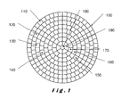
- Figure 1 illustrates a plan view of a polar grid micro-mirror array 100 comprising a plurality of micro-mirror elements arranged in eight concentric rings 110, 120, 130, 140, 150, 160, 170, 180 around a central micro-mirror element 190.
- each ring 110, 120, 130, 140, 150, 160, 170, 180 comprises a different number micro-mirror elements as shown and the illustrated array 100 comprises one hundred and nine micro-mirror elements.
- the array may comprise any suitable number of micro-mirror elements arranged in a regular or irregular pattern within the array.
- the array is not limited to a polar grid array.
- groups of elements within the array can operate as individual sections, the elements within each section having substantially the same properties. The properties of each section may be the same or different to other sections within the array.
- the array 100 may be divided so that rings 110, 120, 130, 140, 150 comprise an outer section and rings 160, 170, 180 together with the central micro-mirror element comprise an inner section, the inner and outer sections being controlled to tilt independently of one another.
- the array 100 may be divided in other ways to provide sections which can be controlled to tilt independently of one another in accordance with a particular implementation thereof.
- the micro-mirror array is equipped with capacitance measurement circuits from which a voltage-tilt angle characteristic of each micro-mirror element is obtained indirectly by measuring the capacitance of each micro-mirror element as it tilts.
- a micro-mirror element arrangement 200 is shown.
- the arrangement 200 comprises a micro-mirror element 210 which is mounted at a pivot point or tilt axis 220 about which it can tilt in accordance with applied voltage.
- Two measurement electrodes 230, 240 are provided which are mounted on a support 250 and are equally spaced from the pivot point or tilt axis 220.
- Two actuation electrodes 260, 270 are also provided on the support 250 adjacent respective ones of the measurement electrodes 230, 240. Each actuation electrode 260, 270 is spaced at the same distance from the pivot point or tilt axis 220 and its associated measurement electrode 230, 240.
- the micro-mirror element 210 is shown in a neutral or substantially horizontal position. It will be appreciated, however, that in certain applications, the neutral position may be at an angle to the horizontal.
- separate electrodes are provided for actuation and capacitance measurement on each side of the pivot point or tilt axis 220.
- the positioning and size of the measurement electrodes 230, 240 can be optimised so that the capacitance measurement is more sensitive than in an arrangement where a single electrode is provided for both actuation of the tilting and measurement of the capacitance induced by the tilting of the micro-mirror element 210. It will be appreciated that the position and size of the actuation electrodes 260, 270 can also be optimised.
- actuation electrode 260 When an actuation voltage is applied to actuation electrode 260, as shown in Figure 3 , the micro-mirror element 210 tilts about the pivot point or tilt axis 220 and a capacitance 290 can be measured at the measurement electrode 240.
- This capacitance 290 when compared to the capacitance in the neutral or previous position provides a change in capacitance which corresponds to the tilt angle, ⁇ 1 , when measured from the horizontal as indicated by dotted line 280.
- an actuation voltage applied to actuation electrode 270 causes the micro-mirror element 210 to tilt about the pivot point or tilt axis 220 and to produce a capacitance 290' that can be measured at the measurement electrode 230 as shown.
- This capacitance 290' when compared to the capacitance in the neutral or previous position provides a change in capacitance which corresponds to the tilt angle, ⁇ 2 , when measured from the horizontal as indicated by dotted line 280.
- the horizontal as indicated by dotted line 280 is considered to be the neutral position, but it will be appreciated that any other position can be chosen as the neutral position.
- the tilt angle can be measured from a previous position of the micro-mirror element 210 which is not horizontal.
- the value of the tilt angle ⁇ 2 may be the same as, or different from, the value of the tilt angle ⁇ 1 .
- a stopper is associated with each actuation and measurement electrode pair which serves to limit the tilt angle of the micro-mirror element about the pivot point or tilt axis.
- Each stopper is preferably located adjacent the measurement electrodes 230, 240, but it will be appreciated that the stoppers may be located at any other suitable location.
- each stopper of the pair can be spaced at a different distance from the pivot point or tilt axis 220.
- each stopper of the pair is spaced at the same distance from the pivot point or tilt axis 220.
- the height/position combination for each stopper is used to determine a reference tilt angles for the method as described below with reference to Figure 5 below.
- the tilt angle of each micro-mirror element will be determined in accordance with its location within the micro-mirror array, for example, in accordance with the radius of the polar grid array.
- the tilt angle of each micro-mirror element at a different radius within the polar grid, as indicated by rings 110, 120, 130, 140, 150, 160, 170, 180, is different.
- the tilt angle of the central micro-mirror element 190 may be different or the same as ring 180.
- the polar grid may be divided so that the micro-mirror elements in the outer section of the polar grid are tilted to a different extent when compared to the micro-mirror elements in the inner section of the polar grid.
- the first step in the method is to define two or more reference tilt angles for the micro-mirror array, step 520.
- Each of these reference tilt angles is obtained using stopper heights and an optical metrology method or any other suitable method.
- the micro-mirror element is located on one stopper and the associated tilt angle measured, and then the micro-mirror element is moved to be located on another stopper and that associated tilt angle measured. These measured tilt angles form the reference tilt angles.
- the stoppers used for the determination of the reference tilt angles may be located relative to the same pivot point or tilt axis or may be located relative to different pivot points or tilt axes.
- the reference tilt angles may be chosen to be 2° and 5°, for example. Naturally, other reference tilt angles may be chosen with difference values being chosen for different pivot points or tilt axes.
- these measurements are performed for only one micro-mirror element per micro-mirror array. In another embodiment, the measurements may be performed for a few micro-mirror elements within a micro-mirror array. By only obtaining the measurements for at most a few micro-mirror elements, the calibration process can be speeded up significantly.
- the corresponding capacitance value is measured for each micro-mirror element in the array, step 530. From these measurements, a table of capacitance values is generated for each of the two reference angles for all micro-mirror elements in the array, step 540. The table is completed by interpolating capacitance values for intermediate tilt angles for each micro-mirror element in the array, step 550. The table provides a capacitance-tilt angle characteristic for each micro-mirror element in the array.
- the next step is to perform a voltage sweep and simultaneously measure the capacitance values for each micro-mirror element in the array, step 560. For a matching capacitance value, the corresponding voltage is noted and added to the table to provide a voltage-tilt angle characteristic for each micro-mirror element in the micro-mirror array. The voltage-tilt angle characteristic and the capacitance-tilt angle characteristic are then stored in a memory for use during a built-in self-calibration process for the particular micro-mirror array, step 570.
- step 520 Whilst the step of defining the reference tilt angles, step 520, needs to be performed before the micro-mirror array can be implemented, it will readily be understood that the following steps can be performed at run-time, thus enabling run-time calibration once the micro-mirror array is incorporated into a device.
- steps 530 to 560 can be performed simultaneously, or in parallel, for all the micro-mirror elements in the array, thus making the calibration process very fast.
- the calibration process is carried out using a calibration system which is built into the micro-mirror array. As only few additional logic circuits and memory are required to support the calibration procedure, the self-calibration process is cost effective.
- FIG. 6 A block diagram of a micro-mirror array device in accordance with the present invention is shown in Figure 6 .
- a calibration system 600 is shown.
- the system 600 comprises a micro-mirror array device 610 which is connected to an actuation module 620 and a capacitance measurement module 630.
- Connected to the capacitance measurement module 630 is an interpolation module 640 which is, in turn, connected to a memory 650.
- a microcontroller 660 is connected to the actuation module 620 and the memory 650.
- the actuation module 620 applies a voltage to the micro-mirror array elements in the micro-mirror array device 610 to provide the voltage sweep (step 560) as described above with reference to Figure 5 .
- the capacitance measurement module 630 measures the capacitance values generated during the voltage sweep.
- the interpolation module 640 determines the interpolated capacitance values (step 550) and passes them to the memory 650.
- the microcontroller 660 controls the operation of the actuation module 620.
- the actuation module 620 comprises a plurality of electrodes as described above with reference to Figures 2 to 4 for applying a driving voltage each micro-mirror element or group of such micro-mirror elements.
- the capacitance measurement module 630 comprises a plurality of sensing electrodes for sensing the capacitance induced due to the tilting of the each micro-mirror element or group of micro-mirror elements.
- the actuation module 620 may also be utilised during operation of the micro-mirror array device as well as during its self-calibration process.
- the capacitance measurement module may also be utilised during operation of the micro-mirror array device.
Landscapes
- Physics & Mathematics (AREA)
- General Physics & Mathematics (AREA)
- Optics & Photonics (AREA)
- Mechanical Light Control Or Optical Switches (AREA)
- Mounting And Adjusting Of Optical Elements (AREA)
- Micromachines (AREA)
Abstract
Description
- The present invention relates to calibration of micro-mirror array devices, and is more particularly, although not exclusively, concerned with the self-calibration of such array devices when used as a variable focal length lens.
- Micro-mirror array devices are devices comprising a plurality of microscopically small mirrors arranged in an array. Such devices comprise micro-electromechanical systems (MEMS) devices whose states are controlled by a voltage between electrodes located around the array.
- Micro-mirror array devices are operated to tilt along a certain axis (or axes) in order to deflect incident light. Typically, the tilt of the micro-mirror is controlled by the actuation of electrodes associated with the micro-mirror, for example, by using an applied voltage.
- Characterisation of voltage against tilt angle for a given micro-mirror device is important in evaluating its performance. Furthermore, this relationship of voltage against tilt angle is also important in calibrating a micro-mirror for use in a certain application, for example, in "smart" lenses where micro-mirrors are used in variable focal length lenses to make zoom lenses. In addition, obtaining or characterising the voltage-tilt angle relationship at run-time is often desirable to support run-time calibration.
- Current methods used for characterising voltage against tilt angle of a micro-mirror typically comprise optical metrology techniques. In such techniques, the micro-mirror is inspected using microscopes of some sort. These methods are quite sensitive, reasonably fast and suitable in many cases where characterisation has to be performed only once before the device is put to use.
- These optical metrology techniques are not suitable in applications where run-time characterisation is required, for example, where the micro-mirror array device is configured as a variable focal length lens. This is because such metrology systems tend to be time consuming, for example, in order to characterise every micro-mirror element in a micro-mirror array comprising 350,000 micro-mirror elements may require more than 30 minutes. This limits the production throughput, that is, the number of micro-mirror arrays that can be produced in a given period of time.
- In addition, optical metrology methods cannot be employed for online or run-time calibration. If the voltage-tilt angle characteristic drifts over a period of operation of a micro-mirror array device, it is not possible to take into account that drift as re-characterisation of voltage-tilt angle characteristic cannot be performed once the micro-mirror array device is operational.
- It is therefore an object of the present invention to provide a built-in self calibration method for a micro-mirror array device operating as a variable focal length lens.
- It is another object of the present invention to provide a built-in self calibration for micro-mirror array devices operating as light modulating devices.
- It is a further object of the present invention to provide a micro-mirror array device that supports run-time calibration in addition to its main functionality.
- In accordance with a first aspect of the present invention, there is provided a method of determining a voltage-tilt angle characteristic for a micro-mirror array, the micro-mirror array comprising a plurality of micro-mirror elements, the method comprising the steps of:
- a) defining a number of reference tilt angles for the micro-mirror array;
- b) determining an electrical measurement for each micro-mirror element corresponding to each reference tilt angle;
- c) interpolating electrical measurements between reference tilt angles for each micro-mirror element;
- d) applying a voltage sweep to the micro-mirror array;
- e) simultaneously measuring electrical values for each micro-mirror element during the voltage sweep; and
- f) using the measured electrical values to determine the voltage-tilt angle characteristic.
- Advantageously, step f) comprises the additional steps of:
- f1) matching measured electrical values with determined electrical values; and
- f2) associating the applied voltage with the tilt angle for each matching electrical value.
- In one embodiment, steps b) to f) are performed simultaneously for all micro-mirror elements in the micro-mirror array.
- The method comprises the step of storing the voltage-tilt angle characteristic for each micro-mirror element in the micro-mirror array.
- In another embodiment, the method may further comprise using the stored voltage-tilt angle characteristic for each micro-mirror element to adjust an output of the micro-mirror array.
- In one embodiment of the present invention, the electrical measurements are capacitance measurements.
- In accordance with another aspect of the present invention, there is provided a calibration system for a micro-mirror array, the micro-mirror array having a predetermined number of reference tilt angles, the calibration system comprising:
- an actuation module for applying a voltage sweep to the micro-mirror array;
- an electrical measurement module for measuring electrical values generated by the voltage sweep;
- an interpolation module for interpolating electrical values corresponding to the reference tilt angles; and
- a memory for storing voltage-tilt angle characteristics for each micro-memory element.
- The system further comprises a controller for controlling the operation of the actuation module during the voltage sweep. In addition, the controller may control the operation of the micro-mirror elements in accordance with the stored voltage-tilt angle characteristics.
- The electrical measurement module may be a capacitance measurement module.
- For a better understanding of the present invention, reference will now be made, by way of example only, to the accompanying drawings in which:-
-
Figure 1 illustrates a micro-mirror array device in accordance with the present invention; -
Figure 2 is a schematic illustration of a micro-mirror element in accordance with the present invention in a neutral position; -
Figures 3 and4 are similar toFigure 2 but illustrate the micro-mirror element in a first and a second tilt position respectively; -
Figure 5 illustrates a flow chart for a calibration method in accordance with the present invention; and -
Figure 6 illustrates a block diagram of a calibration system in accordance with the present invention. - The present invention will be described with respect to particular embodiments and with reference to certain drawings but the invention is not limited thereto. The drawings described are only schematic and are non-limiting. In the drawings, the size of some of the elements may be exaggerated and not drawn on scale for illustrative purposes.
- It will be understood that the terms "vertical" and "horizontal" are used herein refer to particular orientations of the Figures and these terms are not limitations to the specific embodiments described herein.
- Current methods for calibrating micro-mirror array devices involve employing optical metrology systems to characterise a voltage-tilt angle profile or characteristic for every micro-mirror element in the micro-mirror array device. Once the voltage-tilt angle characteristic of every micro-mirror element is known, any two micro-mirror elements in the micro-mirror array can be tilted to the same tilt angle or position by applying a voltage which is appropriate for each micro-mirror element.
- In a particular implementation of a micro-mirror array device, the device operates as a variable focal length lens. In order to operate as a variable focal length lens, the micro-mirror array device can be considered to be an analogue device as it needs to be able to provide more than three tilt positions. This is in contrast to digital micro-mirror array devices where tilting is only possible in one of three positions. Matching of tilt angles of a micro-mirror array is an important parameter in order to evaluate the quality of the resulting device in which the micro-mirror array is implemented. When a given voltage is applied to any two or more micro-mirror elements in the array, each micro-mirror element should ideally have the same tilt angle. In reality, there is a mismatch of the tilt angles of these elements for a given applied voltage, and the smaller the value of the mismatch, the higher the quality of the micro-mirror array.
-
Figure 1 illustrates a plan view of a polargrid micro-mirror array 100 comprising a plurality of micro-mirror elements arranged in eightconcentric rings micro-mirror element 190. In this array, eachring array 100 comprises one hundred and nine micro-mirror elements. - However, it will be appreciated that the array may comprise any suitable number of micro-mirror elements arranged in a regular or irregular pattern within the array. In addition, the array is not limited to a polar grid array. Moreover, groups of elements within the array can operate as individual sections, the elements within each section having substantially the same properties. The properties of each section may be the same or different to other sections within the array.
- In one embodiment, the
array 100 may be divided so that rings 110, 120, 130, 140, 150 comprise an outer section and rings 160, 170, 180 together with the central micro-mirror element comprise an inner section, the inner and outer sections being controlled to tilt independently of one another. - It will be appreciated that the
array 100 may be divided in other ways to provide sections which can be controlled to tilt independently of one another in accordance with a particular implementation thereof. - In accordance with the present invention, the micro-mirror array is equipped with capacitance measurement circuits from which a voltage-tilt angle characteristic of each micro-mirror element is obtained indirectly by measuring the capacitance of each micro-mirror element as it tilts.
- Although the present invention is described with reference to capacitance measurement circuits, it will be appreciated that other forms of electrical measurement may be used, for example, inductance measurements.
- The operation of the capacitance measurement is described below with reference to
Figures 2 to 4 . InFigure 2 , amicro-mirror element arrangement 200 is shown. Thearrangement 200 comprises amicro-mirror element 210 which is mounted at a pivot point ortilt axis 220 about which it can tilt in accordance with applied voltage. Twomeasurement electrodes support 250 and are equally spaced from the pivot point ortilt axis 220. Twoactuation electrodes support 250 adjacent respective ones of themeasurement electrodes actuation electrode tilt axis 220 and its associatedmeasurement electrode micro-mirror element 210 is shown in a neutral or substantially horizontal position. It will be appreciated, however, that in certain applications, the neutral position may be at an angle to the horizontal. - In the embodiment shown in
Figure 2 , separate electrodes are provided for actuation and capacitance measurement on each side of the pivot point ortilt axis 220. This decouples actuation of themicro-mirror element 210 and measurement of the tilt angle. In addition, the positioning and size of themeasurement electrodes micro-mirror element 210. It will be appreciated that the position and size of theactuation electrodes - When an actuation voltage is applied to
actuation electrode 260, as shown inFigure 3 , themicro-mirror element 210 tilts about the pivot point ortilt axis 220 and acapacitance 290 can be measured at themeasurement electrode 240. Thiscapacitance 290, when compared to the capacitance in the neutral or previous position provides a change in capacitance which corresponds to the tilt angle, θ1, when measured from the horizontal as indicated bydotted line 280. - Similarly, in
Figure 4 , an actuation voltage applied toactuation electrode 270 causes themicro-mirror element 210 to tilt about the pivot point ortilt axis 220 and to produce a capacitance 290' that can be measured at themeasurement electrode 230 as shown. This capacitance 290', when compared to the capacitance in the neutral or previous position provides a change in capacitance which corresponds to the tilt angle, θ2, when measured from the horizontal as indicated bydotted line 280. - In
Figures 3 and4 , the horizontal as indicated bydotted line 280 is considered to be the neutral position, but it will be appreciated that any other position can be chosen as the neutral position. In addition, the tilt angle can be measured from a previous position of themicro-mirror element 210 which is not horizontal. - It will be appreciated that the value of the tilt angle θ2 may be the same as, or different from, the value of the tilt angle θ1. By measuring the change in capacitance in each case, the tilt angle of the
micro-mirror element 210 due to an actuation voltage applied toactuation electrodes measurement electrodes - Although not shown, a stopper is associated with each actuation and measurement electrode pair which serves to limit the tilt angle of the micro-mirror element about the pivot point or tilt axis. Each stopper is preferably located adjacent the
measurement electrodes - If pairs of stoppers have the same height, each stopper of the pair can be spaced at a different distance from the pivot point or
tilt axis 220. Alternatively, if the pairs of stoppers have different heights, each stopper of the pair is spaced at the same distance from the pivot point ortilt axis 220. The height/position combination for each stopper is used to determine a reference tilt angles for the method as described below with reference toFigure 5 below. - When a micro-mirror array device having a
polar grid array 100 as shown inFigure 1 is to be used as a variable focal length lens, the tilt angle of each micro-mirror element will be determined in accordance with its location within the micro-mirror array, for example, in accordance with the radius of the polar grid array. The tilt angle of each micro-mirror element at a different radius within the polar grid, as indicated byrings micro-mirror element 190 may be different or the same asring 180. As described above, the polar grid may be divided so that the micro-mirror elements in the outer section of the polar grid are tilted to a different extent when compared to the micro-mirror elements in the inner section of the polar grid. - In accordance with the present invention, the method for determining a voltage-tilt angle characteristic of each micro-mirror element is described below with reference to
Figure 5 . - Having provided a micro-mirror array,
step 510, the first step in the method is to define two or more reference tilt angles for the micro-mirror array,step 520. Each of these reference tilt angles is obtained using stopper heights and an optical metrology method or any other suitable method. The micro-mirror element is located on one stopper and the associated tilt angle measured, and then the micro-mirror element is moved to be located on another stopper and that associated tilt angle measured. These measured tilt angles form the reference tilt angles. The stoppers used for the determination of the reference tilt angles may be located relative to the same pivot point or tilt axis or may be located relative to different pivot points or tilt axes. The reference tilt angles may be chosen to be 2° and 5°, for example. Naturally, other reference tilt angles may be chosen with difference values being chosen for different pivot points or tilt axes. - In one embodiment, these measurements are performed for only one micro-mirror element per micro-mirror array. In another embodiment, the measurements may be performed for a few micro-mirror elements within a micro-mirror array. By only obtaining the measurements for at most a few micro-mirror elements, the calibration process can be speeded up significantly.
- For each of these reference tilt angles, the corresponding capacitance value is measured for each micro-mirror element in the array,
step 530. From these measurements, a table of capacitance values is generated for each of the two reference angles for all micro-mirror elements in the array,step 540. The table is completed by interpolating capacitance values for intermediate tilt angles for each micro-mirror element in the array,step 550. The table provides a capacitance-tilt angle characteristic for each micro-mirror element in the array. - The next step is to perform a voltage sweep and simultaneously measure the capacitance values for each micro-mirror element in the array,
step 560. For a matching capacitance value, the corresponding voltage is noted and added to the table to provide a voltage-tilt angle characteristic for each micro-mirror element in the micro-mirror array. The voltage-tilt angle characteristic and the capacitance-tilt angle characteristic are then stored in a memory for use during a built-in self-calibration process for the particular micro-mirror array,step 570. - Whilst the step of defining the reference tilt angles,
step 520, needs to be performed before the micro-mirror array can be implemented, it will readily be understood that the following steps can be performed at run-time, thus enabling run-time calibration once the micro-mirror array is incorporated into a device. - In addition, steps 530 to 560 can be performed simultaneously, or in parallel, for all the micro-mirror elements in the array, thus making the calibration process very fast.
- It will readily be appreciated that, as there is an interpolation step for determining capacitance values for intermediate tilt angles, the more reference tilt angles used, the more accurate the interpolation will be.
- The calibration process is carried out using a calibration system which is built into the micro-mirror array. As only few additional logic circuits and memory are required to support the calibration procedure, the self-calibration process is cost effective.
- A block diagram of a micro-mirror array device in accordance with the present invention is shown in
Figure 6 . InFigure 6 , acalibration system 600 is shown. Thesystem 600 comprises amicro-mirror array device 610 which is connected to anactuation module 620 and acapacitance measurement module 630. Connected to thecapacitance measurement module 630 is aninterpolation module 640 which is, in turn, connected to amemory 650. Amicrocontroller 660 is connected to theactuation module 620 and thememory 650. - The
actuation module 620 applies a voltage to the micro-mirror array elements in themicro-mirror array device 610 to provide the voltage sweep (step 560) as described above with reference toFigure 5 . Thecapacitance measurement module 630 measures the capacitance values generated during the voltage sweep. Theinterpolation module 640 determines the interpolated capacitance values (step 550) and passes them to thememory 650. Themicrocontroller 660 controls the operation of theactuation module 620. - The
actuation module 620 comprises a plurality of electrodes as described above with reference toFigures 2 to 4 for applying a driving voltage each micro-mirror element or group of such micro-mirror elements. Similarly, thecapacitance measurement module 630 comprises a plurality of sensing electrodes for sensing the capacitance induced due to the tilting of the each micro-mirror element or group of micro-mirror elements. - In one embodiment, the
actuation module 620 may also be utilised during operation of the micro-mirror array device as well as during its self-calibration process. Similarly, the capacitance measurement module may also be utilised during operation of the micro-mirror array device. - Although the present invention has been described with reference to a polar grid micro-mirror array operating as a variable focal length lens, it will be appreciated that the calibration method and system of the present invention may also be applied to other micro-mirror array devices, for example, light modulating devices.
Claims (10)
- A method of determining a voltage-tilt angle characteristic for a micro-mirror array (100), the micro-mirror array comprising a plurality of micro-mirror elements, the method comprising the steps of:a) defining a number of reference tilt angles for the micro-mirror array;b) determining an electrical measurement for each micro-mirror element corresponding to each reference tilt angle;c) interpolating electrical measurements between reference tilt angles for each micro-mirror element;d) applying a voltage sweep to the micro-mirror array (100);e) simultaneously measuring electrical values for each micro-mirror element during the voltage sweep; andf) using the measured electrical values to determine the voltage-tilt angle characteristic.
- A method according to claim 1, wherein step f) comprises:f1) matching measured electrical values with determined
electrical values; andf2) associating the applied voltage with the tilt angle for each
matching electrical value. - A method according to claim 1 or 2, wherein steps b) to f) are performed simultaneously for all micro-mirror elements in the micro-mirror array (100).
- A method according to any one of the preceding claims, further comprising the step of storing the voltage-tilt angle characteristic for each micro-mirror element in the micro-mirror array (100).
- A method according to claim 4, further comprising the step of using the stored voltage-tilt angle characteristic for each micro-mirror element to adjust an output of the micro-mirror array (100).
- A method according to any one of the preceding claims, wherein the electrical measurements are capacitance measurements.
- A calibration system (600) for a micro-mirror array (100; 610), the micro-mirror array having a predetermined number of reference tilt angles, the calibration system comprising:an actuation module (620) for applying a voltage sweep to the micro-mirror array (610);an electrical measurement module (630) for measuring electrical values generated by the voltage sweep;an interpolation module (640) for interpolating electrical values corresponding to the reference tilt angles; anda memory (650) for storing voltage-tilt angle characteristics for each micro-memory element.
- A calibration system according to claim 7, further comprising a controller (660) for controlling the operation of the actuation module (620) during the voltage sweep.
- A calibration system according to claim 8, wherein the controller controls operation of the micro-mirror elements in accordance with the stored voltage-tilt angle characteristics.
- A calibration system according to any one of claims 7 to 9, wherein the electrical measurement module comprises a capacitance measurement module.
Priority Applications (3)
| Application Number | Priority Date | Filing Date | Title |
|---|---|---|---|
| EP12152010.0A EP2618201B1 (en) | 2012-01-20 | 2012-01-20 | Calibration of micro-mirror arrays |
| JP2013008516A JP2013148906A (en) | 2012-01-20 | 2013-01-21 | Correction of micromirror array |
| US13/746,149 US9201241B2 (en) | 2012-01-20 | 2013-01-21 | Calibration of micro-mirror arrays |
Applications Claiming Priority (1)
| Application Number | Priority Date | Filing Date | Title |
|---|---|---|---|
| EP12152010.0A EP2618201B1 (en) | 2012-01-20 | 2012-01-20 | Calibration of micro-mirror arrays |
Publications (2)
| Publication Number | Publication Date |
|---|---|
| EP2618201A1 true EP2618201A1 (en) | 2013-07-24 |
| EP2618201B1 EP2618201B1 (en) | 2015-11-04 |
Family
ID=45507603
Family Applications (1)
| Application Number | Title | Priority Date | Filing Date |
|---|---|---|---|
| EP12152010.0A Active EP2618201B1 (en) | 2012-01-20 | 2012-01-20 | Calibration of micro-mirror arrays |
Country Status (3)
| Country | Link |
|---|---|
| US (1) | US9201241B2 (en) |
| EP (1) | EP2618201B1 (en) |
| JP (1) | JP2013148906A (en) |
Cited By (1)
| Publication number | Priority date | Publication date | Assignee | Title |
|---|---|---|---|---|
| DE102016212260A1 (en) * | 2016-07-05 | 2017-06-22 | Carl Zeiss Smt Gmbh | Device for measuring an orientation of a module |
Families Citing this family (5)
| Publication number | Priority date | Publication date | Assignee | Title |
|---|---|---|---|---|
| DE102017209730B4 (en) * | 2017-06-08 | 2021-05-27 | Osram Gmbh | LIGHTING DEVICE WITH A LIGHT SOURCE TO EMISSION AND USE LIGHTING LIGHT |
| CN109426091B (en) * | 2017-08-31 | 2021-01-29 | 京东方科技集团股份有限公司 | Exposure apparatus, exposure method, and photolithography method |
| US11820649B2 (en) | 2018-05-18 | 2023-11-21 | Lawrence Livermore National Security, Llc | Position sensing circuit for an electrostatically driven MEMS device |
| EP3926385B1 (en) | 2020-06-16 | 2024-05-15 | Carl Zeiss Microscopy GmbH | Digital microscope and microscopic set |
| TWI900906B (en) * | 2023-03-17 | 2025-10-11 | 財團法人工業技術研究院 | Array objective lens module and optical interference microscopy device |
Citations (4)
| Publication number | Priority date | Publication date | Assignee | Title |
|---|---|---|---|---|
| US20030025982A1 (en) * | 2001-07-31 | 2003-02-06 | Axsun Technologies, Inc. | System and method for tilt mirror calibration due to capacitive sensor drift |
| US6625341B1 (en) * | 2000-06-12 | 2003-09-23 | Vlad J. Novotny | Optical cross connect switching array system with electrical and optical position sensitive detection |
| US20080137173A1 (en) * | 2006-12-12 | 2008-06-12 | Stereo Display, Inc. | Discretely controlled micromirror array device with segmented electrodes |
| US20080231141A1 (en) * | 2002-11-06 | 2008-09-25 | Matsushita Electric Industrial Co., Ltd. | Microactuator with Displacement Sensing Function and Deformable Mirror Including the Microactuator |
Family Cites Families (9)
| Publication number | Priority date | Publication date | Assignee | Title |
|---|---|---|---|---|
| US5485304A (en) * | 1994-07-29 | 1996-01-16 | Texas Instruments, Inc. | Support posts for micro-mechanical devices |
| US6963359B1 (en) * | 1997-10-23 | 2005-11-08 | Fuji Photo Film Co., Ltd. | Electronic still camera, instant printer and instant film |
| US6661637B2 (en) * | 1998-03-10 | 2003-12-09 | Mcintosh Robert B. | Apparatus and method to angularly position micro-optical elements |
| JP2005326620A (en) * | 2004-05-14 | 2005-11-24 | Fujitsu Ltd | Micro mirror element |
| JP4357412B2 (en) * | 2004-12-28 | 2009-11-04 | 三洋電機株式会社 | Reflector |
| US7830561B2 (en) * | 2005-03-16 | 2010-11-09 | The Trustees Of Columbia University In The City Of New York | Lensless imaging with controllable apertures |
| JP4464374B2 (en) * | 2006-08-18 | 2010-05-19 | 日本電信電話株式会社 | Micromirror device and optical switch |
| US20100141852A1 (en) * | 2008-12-05 | 2010-06-10 | Robe Lighting S.R.O. | Distortion Corrected Improved Beam Angle Range, Higher Output Digital Luminaire System |
| US8786170B2 (en) * | 2010-08-24 | 2014-07-22 | Delta Electronics, Inc. | Optical system for providing telecentric light beam |
-
2012
- 2012-01-20 EP EP12152010.0A patent/EP2618201B1/en active Active
-
2013
- 2013-01-21 JP JP2013008516A patent/JP2013148906A/en active Pending
- 2013-01-21 US US13/746,149 patent/US9201241B2/en active Active
Patent Citations (4)
| Publication number | Priority date | Publication date | Assignee | Title |
|---|---|---|---|---|
| US6625341B1 (en) * | 2000-06-12 | 2003-09-23 | Vlad J. Novotny | Optical cross connect switching array system with electrical and optical position sensitive detection |
| US20030025982A1 (en) * | 2001-07-31 | 2003-02-06 | Axsun Technologies, Inc. | System and method for tilt mirror calibration due to capacitive sensor drift |
| US20080231141A1 (en) * | 2002-11-06 | 2008-09-25 | Matsushita Electric Industrial Co., Ltd. | Microactuator with Displacement Sensing Function and Deformable Mirror Including the Microactuator |
| US20080137173A1 (en) * | 2006-12-12 | 2008-06-12 | Stereo Display, Inc. | Discretely controlled micromirror array device with segmented electrodes |
Cited By (1)
| Publication number | Priority date | Publication date | Assignee | Title |
|---|---|---|---|---|
| DE102016212260A1 (en) * | 2016-07-05 | 2017-06-22 | Carl Zeiss Smt Gmbh | Device for measuring an orientation of a module |
Also Published As
| Publication number | Publication date |
|---|---|
| US9201241B2 (en) | 2015-12-01 |
| EP2618201B1 (en) | 2015-11-04 |
| US20130187669A1 (en) | 2013-07-25 |
| JP2013148906A (en) | 2013-08-01 |
Similar Documents
| Publication | Publication Date | Title |
|---|---|---|
| US9201241B2 (en) | Calibration of micro-mirror arrays | |
| KR101975433B1 (en) | A method for calibrating an image capture device | |
| US10062180B2 (en) | Depth sensor calibration and per-pixel correction | |
| US10877257B2 (en) | Phase contrast microscope | |
| TWI757795B (en) | Methods for maintaining gap spacing between an optical probe of a probe system and an optical device of a device under test, and probe systems that perform the methods | |
| CN109283184A (en) | A Surface Defect Measurement Method Based on Spectral Confocal Sensor | |
| CN105408788A (en) | Device and method for micro-electro-mechanical-system photonic switch | |
| EP4456532A1 (en) | Intrinsic parameter testing | |
| CN106468534A (en) | For measure height map and by height map merge into synthesis height map method | |
| KR101652356B1 (en) | optical apparatus for examining pattern image of semiconductor device | |
| US9217861B2 (en) | Micro-mirror arrays | |
| CN104633599A (en) | Method of automatic focusing for patterned moving lamp | |
| KR20190069362A (en) | Displacement measuring device, measuring system and displacement measuring method | |
| CN103090966A (en) | Laser intensity distribution accurate measurement system using single photodetector | |
| JP7059406B2 (en) | Optical member position adjustment support device, optical member position adjustment support method, optical member position adjustment support program, lens device manufacturing method | |
| CN107677456A (en) | A kind of telescope optic axis Detection of Stability method | |
| KR102662778B1 (en) | Sampling optimization method and sampling optimization system for overlay measurement apparatus | |
| CN115236093B (en) | Optical detection system, control method thereof, electronic device, and storage medium | |
| US7569805B2 (en) | Apparatus and method for calibrating a reflecting mirror | |
| CN103968859B (en) | A kind of ultra-large vision field ultraviolet faces the geometric calibration method of limit imager | |
| KR101915264B1 (en) | Method of Measuring the Optical Properties of the Display and Device of Measuring the Same | |
| KR101712545B1 (en) | Apparatus and method for de-focusing of infrared detector | |
| CN104776978B (en) | Array element splicing method based on image cross correlation | |
| US20210063143A1 (en) | Multi-parameter calculation via modal power measurements | |
| US9453763B2 (en) | Tunable light-guide image processor for multi-dimensional imaging |
Legal Events
| Date | Code | Title | Description |
|---|---|---|---|
| PUAI | Public reference made under article 153(3) epc to a published international application that has entered the european phase |
Free format text: ORIGINAL CODE: 0009012 |
|
| AK | Designated contracting states |
Kind code of ref document: A1 Designated state(s): AL AT BE BG CH CY CZ DE DK EE ES FI FR GB GR HR HU IE IS IT LI LT LU LV MC MK MT NL NO PL PT RO RS SE SI SK SM TR |
|
| AX | Request for extension of the european patent |
Extension state: BA ME |
|
| 17P | Request for examination filed |
Effective date: 20131226 |
|
| RBV | Designated contracting states (corrected) |
Designated state(s): AL AT BE BG CH CY CZ DE DK EE ES FI FR GB GR HR HU IE IS IT LI LT LU LV MC MK MT NL NO PL PT RO RS SE SI SK SM TR |
|
| 17Q | First examination report despatched |
Effective date: 20140306 |
|
| GRAP | Despatch of communication of intention to grant a patent |
Free format text: ORIGINAL CODE: EPIDOSNIGR1 |
|
| INTG | Intention to grant announced |
Effective date: 20150520 |
|
| GRAS | Grant fee paid |
Free format text: ORIGINAL CODE: EPIDOSNIGR3 |
|
| GRAA | (expected) grant |
Free format text: ORIGINAL CODE: 0009210 |
|
| AK | Designated contracting states |
Kind code of ref document: B1 Designated state(s): AL AT BE BG CH CY CZ DE DK EE ES FI FR GB GR HR HU IE IS IT LI LT LU LV MC MK MT NL NO PL PT RO RS SE SI SK SM TR |
|
| REG | Reference to a national code |
Ref country code: GB Ref legal event code: FG4D |
|
| REG | Reference to a national code |
Ref country code: CH Ref legal event code: EP |
|
| REG | Reference to a national code |
Ref country code: AT Ref legal event code: REF Ref document number: 759608 Country of ref document: AT Kind code of ref document: T Effective date: 20151115 |
|
| REG | Reference to a national code |
Ref country code: IE Ref legal event code: FG4D |
|
| REG | Reference to a national code |
Ref country code: DE Ref legal event code: R096 Ref document number: 602012012066 Country of ref document: DE |
|
| REG | Reference to a national code |
Ref country code: FR Ref legal event code: PLFP Year of fee payment: 5 |
|
| REG | Reference to a national code |
Ref country code: NL Ref legal event code: MP Effective date: 20151104 |
|
| REG | Reference to a national code |
Ref country code: LT Ref legal event code: MG4D |
|
| REG | Reference to a national code |
Ref country code: AT Ref legal event code: MK05 Ref document number: 759608 Country of ref document: AT Kind code of ref document: T Effective date: 20151104 |
|
| PG25 | Lapsed in a contracting state [announced via postgrant information from national office to epo] |
Ref country code: LT Free format text: LAPSE BECAUSE OF FAILURE TO SUBMIT A TRANSLATION OF THE DESCRIPTION OR TO PAY THE FEE WITHIN THE PRESCRIBED TIME-LIMIT Effective date: 20151104 Ref country code: HR Free format text: LAPSE BECAUSE OF FAILURE TO SUBMIT A TRANSLATION OF THE DESCRIPTION OR TO PAY THE FEE WITHIN THE PRESCRIBED TIME-LIMIT Effective date: 20151104 Ref country code: NO Free format text: LAPSE BECAUSE OF FAILURE TO SUBMIT A TRANSLATION OF THE DESCRIPTION OR TO PAY THE FEE WITHIN THE PRESCRIBED TIME-LIMIT Effective date: 20160204 Ref country code: IT Free format text: LAPSE BECAUSE OF FAILURE TO SUBMIT A TRANSLATION OF THE DESCRIPTION OR TO PAY THE FEE WITHIN THE PRESCRIBED TIME-LIMIT Effective date: 20151104 Ref country code: NL Free format text: LAPSE BECAUSE OF FAILURE TO SUBMIT A TRANSLATION OF THE DESCRIPTION OR TO PAY THE FEE WITHIN THE PRESCRIBED TIME-LIMIT Effective date: 20151104 Ref country code: IS Free format text: LAPSE BECAUSE OF FAILURE TO SUBMIT A TRANSLATION OF THE DESCRIPTION OR TO PAY THE FEE WITHIN THE PRESCRIBED TIME-LIMIT Effective date: 20160304 Ref country code: ES Free format text: LAPSE BECAUSE OF FAILURE TO SUBMIT A TRANSLATION OF THE DESCRIPTION OR TO PAY THE FEE WITHIN THE PRESCRIBED TIME-LIMIT Effective date: 20151104 |
|
| PG25 | Lapsed in a contracting state [announced via postgrant information from national office to epo] |
Ref country code: GR Free format text: LAPSE BECAUSE OF FAILURE TO SUBMIT A TRANSLATION OF THE DESCRIPTION OR TO PAY THE FEE WITHIN THE PRESCRIBED TIME-LIMIT Effective date: 20160205 Ref country code: FI Free format text: LAPSE BECAUSE OF FAILURE TO SUBMIT A TRANSLATION OF THE DESCRIPTION OR TO PAY THE FEE WITHIN THE PRESCRIBED TIME-LIMIT Effective date: 20151104 Ref country code: RS Free format text: LAPSE BECAUSE OF FAILURE TO SUBMIT A TRANSLATION OF THE DESCRIPTION OR TO PAY THE FEE WITHIN THE PRESCRIBED TIME-LIMIT Effective date: 20151104 Ref country code: BE Free format text: LAPSE BECAUSE OF NON-PAYMENT OF DUE FEES Effective date: 20160131 Ref country code: AT Free format text: LAPSE BECAUSE OF FAILURE TO SUBMIT A TRANSLATION OF THE DESCRIPTION OR TO PAY THE FEE WITHIN THE PRESCRIBED TIME-LIMIT Effective date: 20151104 Ref country code: SE Free format text: LAPSE BECAUSE OF FAILURE TO SUBMIT A TRANSLATION OF THE DESCRIPTION OR TO PAY THE FEE WITHIN THE PRESCRIBED TIME-LIMIT Effective date: 20151104 Ref country code: LV Free format text: LAPSE BECAUSE OF FAILURE TO SUBMIT A TRANSLATION OF THE DESCRIPTION OR TO PAY THE FEE WITHIN THE PRESCRIBED TIME-LIMIT Effective date: 20151104 Ref country code: PT Free format text: LAPSE BECAUSE OF FAILURE TO SUBMIT A TRANSLATION OF THE DESCRIPTION OR TO PAY THE FEE WITHIN THE PRESCRIBED TIME-LIMIT Effective date: 20160304 Ref country code: PL Free format text: LAPSE BECAUSE OF FAILURE TO SUBMIT A TRANSLATION OF THE DESCRIPTION OR TO PAY THE FEE WITHIN THE PRESCRIBED TIME-LIMIT Effective date: 20151104 |
|
| PG25 | Lapsed in a contracting state [announced via postgrant information from national office to epo] |
Ref country code: CZ Free format text: LAPSE BECAUSE OF FAILURE TO SUBMIT A TRANSLATION OF THE DESCRIPTION OR TO PAY THE FEE WITHIN THE PRESCRIBED TIME-LIMIT Effective date: 20151104 |
|
| REG | Reference to a national code |
Ref country code: DE Ref legal event code: R097 Ref document number: 602012012066 Country of ref document: DE |
|
| PG25 | Lapsed in a contracting state [announced via postgrant information from national office to epo] |
Ref country code: SM Free format text: LAPSE BECAUSE OF FAILURE TO SUBMIT A TRANSLATION OF THE DESCRIPTION OR TO PAY THE FEE WITHIN THE PRESCRIBED TIME-LIMIT Effective date: 20151104 Ref country code: SK Free format text: LAPSE BECAUSE OF FAILURE TO SUBMIT A TRANSLATION OF THE DESCRIPTION OR TO PAY THE FEE WITHIN THE PRESCRIBED TIME-LIMIT Effective date: 20151104 Ref country code: DK Free format text: LAPSE BECAUSE OF FAILURE TO SUBMIT A TRANSLATION OF THE DESCRIPTION OR TO PAY THE FEE WITHIN THE PRESCRIBED TIME-LIMIT Effective date: 20151104 Ref country code: EE Free format text: LAPSE BECAUSE OF FAILURE TO SUBMIT A TRANSLATION OF THE DESCRIPTION OR TO PAY THE FEE WITHIN THE PRESCRIBED TIME-LIMIT Effective date: 20151104 Ref country code: RO Free format text: LAPSE BECAUSE OF FAILURE TO SUBMIT A TRANSLATION OF THE DESCRIPTION OR TO PAY THE FEE WITHIN THE PRESCRIBED TIME-LIMIT Effective date: 20151104 Ref country code: LU Free format text: LAPSE BECAUSE OF FAILURE TO SUBMIT A TRANSLATION OF THE DESCRIPTION OR TO PAY THE FEE WITHIN THE PRESCRIBED TIME-LIMIT Effective date: 20160120 |
|
| REG | Reference to a national code |
Ref country code: CH Ref legal event code: PL |
|
| PLBE | No opposition filed within time limit |
Free format text: ORIGINAL CODE: 0009261 |
|
| STAA | Information on the status of an ep patent application or granted ep patent |
Free format text: STATUS: NO OPPOSITION FILED WITHIN TIME LIMIT |
|
| PG25 | Lapsed in a contracting state [announced via postgrant information from national office to epo] |
Ref country code: MC Free format text: LAPSE BECAUSE OF FAILURE TO SUBMIT A TRANSLATION OF THE DESCRIPTION OR TO PAY THE FEE WITHIN THE PRESCRIBED TIME-LIMIT Effective date: 20151104 |
|
| 26N | No opposition filed |
Effective date: 20160805 |
|
| PG25 | Lapsed in a contracting state [announced via postgrant information from national office to epo] |
Ref country code: CH Free format text: LAPSE BECAUSE OF NON-PAYMENT OF DUE FEES Effective date: 20160131 Ref country code: LI Free format text: LAPSE BECAUSE OF NON-PAYMENT OF DUE FEES Effective date: 20160131 |
|
| REG | Reference to a national code |
Ref country code: IE Ref legal event code: MM4A |
|
| PG25 | Lapsed in a contracting state [announced via postgrant information from national office to epo] |
Ref country code: SI Free format text: LAPSE BECAUSE OF FAILURE TO SUBMIT A TRANSLATION OF THE DESCRIPTION OR TO PAY THE FEE WITHIN THE PRESCRIBED TIME-LIMIT Effective date: 20151104 |
|
| REG | Reference to a national code |
Ref country code: FR Ref legal event code: PLFP Year of fee payment: 6 |
|
| PG25 | Lapsed in a contracting state [announced via postgrant information from national office to epo] |
Ref country code: BE Free format text: LAPSE BECAUSE OF FAILURE TO SUBMIT A TRANSLATION OF THE DESCRIPTION OR TO PAY THE FEE WITHIN THE PRESCRIBED TIME-LIMIT Effective date: 20151104 |
|
| PG25 | Lapsed in a contracting state [announced via postgrant information from national office to epo] |
Ref country code: IE Free format text: LAPSE BECAUSE OF NON-PAYMENT OF DUE FEES Effective date: 20160120 |
|
| PG25 | Lapsed in a contracting state [announced via postgrant information from national office to epo] |
Ref country code: MT Free format text: LAPSE BECAUSE OF FAILURE TO SUBMIT A TRANSLATION OF THE DESCRIPTION OR TO PAY THE FEE WITHIN THE PRESCRIBED TIME-LIMIT Effective date: 20151104 |
|
| REG | Reference to a national code |
Ref country code: FR Ref legal event code: PLFP Year of fee payment: 7 |
|
| PG25 | Lapsed in a contracting state [announced via postgrant information from national office to epo] |
Ref country code: HU Free format text: LAPSE BECAUSE OF FAILURE TO SUBMIT A TRANSLATION OF THE DESCRIPTION OR TO PAY THE FEE WITHIN THE PRESCRIBED TIME-LIMIT; INVALID AB INITIO Effective date: 20120120 Ref country code: CY Free format text: LAPSE BECAUSE OF FAILURE TO SUBMIT A TRANSLATION OF THE DESCRIPTION OR TO PAY THE FEE WITHIN THE PRESCRIBED TIME-LIMIT Effective date: 20151104 |
|
| PG25 | Lapsed in a contracting state [announced via postgrant information from national office to epo] |
Ref country code: MK Free format text: LAPSE BECAUSE OF FAILURE TO SUBMIT A TRANSLATION OF THE DESCRIPTION OR TO PAY THE FEE WITHIN THE PRESCRIBED TIME-LIMIT Effective date: 20151104 Ref country code: TR Free format text: LAPSE BECAUSE OF FAILURE TO SUBMIT A TRANSLATION OF THE DESCRIPTION OR TO PAY THE FEE WITHIN THE PRESCRIBED TIME-LIMIT Effective date: 20151104 Ref country code: MT Free format text: LAPSE BECAUSE OF FAILURE TO SUBMIT A TRANSLATION OF THE DESCRIPTION OR TO PAY THE FEE WITHIN THE PRESCRIBED TIME-LIMIT Effective date: 20160131 |
|
| PG25 | Lapsed in a contracting state [announced via postgrant information from national office to epo] |
Ref country code: BG Free format text: LAPSE BECAUSE OF FAILURE TO SUBMIT A TRANSLATION OF THE DESCRIPTION OR TO PAY THE FEE WITHIN THE PRESCRIBED TIME-LIMIT Effective date: 20151104 |
|
| PG25 | Lapsed in a contracting state [announced via postgrant information from national office to epo] |
Ref country code: AL Free format text: LAPSE BECAUSE OF FAILURE TO SUBMIT A TRANSLATION OF THE DESCRIPTION OR TO PAY THE FEE WITHIN THE PRESCRIBED TIME-LIMIT Effective date: 20151104 |
|
| P01 | Opt-out of the competence of the unified patent court (upc) registered |
Effective date: 20230513 |
|
| PGFP | Annual fee paid to national office [announced via postgrant information from national office to epo] |
Ref country code: GB Payment date: 20251220 Year of fee payment: 15 |
|
| PGFP | Annual fee paid to national office [announced via postgrant information from national office to epo] |
Ref country code: FR Payment date: 20251217 Year of fee payment: 15 |
|
| PGFP | Annual fee paid to national office [announced via postgrant information from national office to epo] |
Ref country code: DE Payment date: 20251217 Year of fee payment: 15 |