EP2613368B1 - Light emitting diode - Google Patents
Light emitting diode Download PDFInfo
- Publication number
- EP2613368B1 EP2613368B1 EP13150060.5A EP13150060A EP2613368B1 EP 2613368 B1 EP2613368 B1 EP 2613368B1 EP 13150060 A EP13150060 A EP 13150060A EP 2613368 B1 EP2613368 B1 EP 2613368B1
- Authority
- EP
- European Patent Office
- Prior art keywords
- semiconductor layer
- layer
- nitride semiconductor
- light emitting
- emitting diode
- Prior art date
- Legal status (The legal status is an assumption and is not a legal conclusion. Google has not performed a legal analysis and makes no representation as to the accuracy of the status listed.)
- Not-in-force
Links
Images


Classifications
-
- H—ELECTRICITY
- H10—SEMICONDUCTOR DEVICES; ELECTRIC SOLID-STATE DEVICES NOT OTHERWISE PROVIDED FOR
- H10H—INORGANIC LIGHT-EMITTING SEMICONDUCTOR DEVICES HAVING POTENTIAL BARRIERS
- H10H20/00—Individual inorganic light-emitting semiconductor devices having potential barriers, e.g. light-emitting diodes [LED]
- H10H20/80—Constructional details
- H10H20/81—Bodies
- H10H20/822—Materials of the light-emitting regions
- H10H20/824—Materials of the light-emitting regions comprising only Group III-V materials, e.g. GaP
- H10H20/825—Materials of the light-emitting regions comprising only Group III-V materials, e.g. GaP containing nitrogen, e.g. GaN
-
- A—HUMAN NECESSITIES
- A62—LIFE-SAVING; FIRE-FIGHTING
- A62B—DEVICES, APPARATUS OR METHODS FOR LIFE-SAVING
- A62B5/00—Other devices for rescuing from fire
-
- E—FIXED CONSTRUCTIONS
- E04—BUILDING
- E04F—FINISHING WORK ON BUILDINGS, e.g. STAIRS, FLOORS
- E04F19/00—Other details of constructional parts for finishing work on buildings
- E04F19/08—Built-in cupboards; Masks of niches; Covers of holes enabling access to installations
-
- E—FIXED CONSTRUCTIONS
- E06—DOORS, WINDOWS, SHUTTERS, OR ROLLER BLINDS IN GENERAL; LADDERS
- E06C—LADDERS
- E06C9/00—Ladders characterised by being permanently attached to fixed structures, e.g. fire escapes
- E06C9/02—Ladders characterised by being permanently attached to fixed structures, e.g. fire escapes rigidly mounted
-
- E—FIXED CONSTRUCTIONS
- E06—DOORS, WINDOWS, SHUTTERS, OR ROLLER BLINDS IN GENERAL; LADDERS
- E06C—LADDERS
- E06C9/00—Ladders characterised by being permanently attached to fixed structures, e.g. fire escapes
- E06C9/06—Ladders characterised by being permanently attached to fixed structures, e.g. fire escapes movably mounted
- E06C9/08—Ladders characterised by being permanently attached to fixed structures, e.g. fire escapes movably mounted with rigid longitudinal members
-
- F—MECHANICAL ENGINEERING; LIGHTING; HEATING; WEAPONS; BLASTING
- F21—LIGHTING
- F21K—NON-ELECTRIC LIGHT SOURCES USING LUMINESCENCE; LIGHT SOURCES USING ELECTROCHEMILUMINESCENCE; LIGHT SOURCES USING CHARGES OF COMBUSTIBLE MATERIAL; LIGHT SOURCES USING SEMICONDUCTOR DEVICES AS LIGHT-GENERATING ELEMENTS; LIGHT SOURCES NOT OTHERWISE PROVIDED FOR
- F21K9/00—Light sources using semiconductor devices as light-generating elements, e.g. using light-emitting diodes [LED] or lasers
- F21K9/20—Light sources comprising attachment means
- F21K9/23—Retrofit light sources for lighting devices with a single fitting for each light source, e.g. for substitution of incandescent lamps with bayonet or threaded fittings
- F21K9/232—Retrofit light sources for lighting devices with a single fitting for each light source, e.g. for substitution of incandescent lamps with bayonet or threaded fittings specially adapted for generating an essentially omnidirectional light distribution, e.g. with a glass bulb
-
- F—MECHANICAL ENGINEERING; LIGHTING; HEATING; WEAPONS; BLASTING
- F21—LIGHTING
- F21Y—INDEXING SCHEME ASSOCIATED WITH SUBCLASSES F21K, F21L, F21S and F21V, RELATING TO THE FORM OR THE KIND OF THE LIGHT SOURCES OR OF THE COLOUR OF THE LIGHT EMITTED
- F21Y2115/00—Light-generating elements of semiconductor light sources
- F21Y2115/10—Light-emitting diodes [LED]
-
- H—ELECTRICITY
- H10—SEMICONDUCTOR DEVICES; ELECTRIC SOLID-STATE DEVICES NOT OTHERWISE PROVIDED FOR
- H10H—INORGANIC LIGHT-EMITTING SEMICONDUCTOR DEVICES HAVING POTENTIAL BARRIERS
- H10H20/00—Individual inorganic light-emitting semiconductor devices having potential barriers, e.g. light-emitting diodes [LED]
- H10H20/80—Constructional details
- H10H20/81—Bodies
- H10H20/811—Bodies having quantum effect structures or superlattices, e.g. tunnel junctions
-
- H—ELECTRICITY
- H10—SEMICONDUCTOR DEVICES; ELECTRIC SOLID-STATE DEVICES NOT OTHERWISE PROVIDED FOR
- H10H—INORGANIC LIGHT-EMITTING SEMICONDUCTOR DEVICES HAVING POTENTIAL BARRIERS
- H10H20/00—Individual inorganic light-emitting semiconductor devices having potential barriers, e.g. light-emitting diodes [LED]
- H10H20/80—Constructional details
- H10H20/81—Bodies
- H10H20/819—Bodies characterised by their shape, e.g. curved or truncated substrates
-
- H—ELECTRICITY
- H10—SEMICONDUCTOR DEVICES; ELECTRIC SOLID-STATE DEVICES NOT OTHERWISE PROVIDED FOR
- H10H—INORGANIC LIGHT-EMITTING SEMICONDUCTOR DEVICES HAVING POTENTIAL BARRIERS
- H10H20/00—Individual inorganic light-emitting semiconductor devices having potential barriers, e.g. light-emitting diodes [LED]
- H10H20/80—Constructional details
- H10H20/83—Electrodes
- H10H20/831—Electrodes characterised by their shape
- H10H20/8312—Electrodes characterised by their shape extending at least partially through the bodies
-
- H—ELECTRICITY
- H10—SEMICONDUCTOR DEVICES; ELECTRIC SOLID-STATE DEVICES NOT OTHERWISE PROVIDED FOR
- H10H—INORGANIC LIGHT-EMITTING SEMICONDUCTOR DEVICES HAVING POTENTIAL BARRIERS
- H10H20/00—Individual inorganic light-emitting semiconductor devices having potential barriers, e.g. light-emitting diodes [LED]
- H10H20/80—Constructional details
- H10H20/83—Electrodes
- H10H20/832—Electrodes characterised by their material
- H10H20/833—Transparent materials
-
- H—ELECTRICITY
- H10—SEMICONDUCTOR DEVICES; ELECTRIC SOLID-STATE DEVICES NOT OTHERWISE PROVIDED FOR
- H10H—INORGANIC LIGHT-EMITTING SEMICONDUCTOR DEVICES HAVING POTENTIAL BARRIERS
- H10H20/00—Individual inorganic light-emitting semiconductor devices having potential barriers, e.g. light-emitting diodes [LED]
- H10H20/80—Constructional details
- H10H20/84—Coatings, e.g. passivation layers or antireflective coatings
Definitions
- the present disclosure relates to light emitting diodes (LEDs), a method of manufacturing a light emitting diode, a light emitting diode package, and a lighting system.
- LEDs light emitting diodes
- a light emitting diode includes a p-n junction diode having a characteristic of converting electric energy into light energy.
- the p-n junction diode can be formed by combining group III-V elements of the periodic table.
- the LED may represent various colors by adjusting the compositional ratio of compound semiconductors.
- a nitride semiconductor represents superior thermal stability and wide band gap energy so that the nitride semiconductor has been spotlighted in the field of optical devices and high-power electronic devices.
- blue, green, and UV light emitting devices employing the nitride semiconductor have already been developed and extensively used.
- a patterned sapphire substrate (PSS) using a pattern on a substrate is used at a lower portion of a light emitting diode chip, and roughening is used at an upper portion of the light emitting diode chip so that light extraction efficiency may be improved.
- PSS patterned sapphire substrate
- the improvement in the light extraction efficiency is required.
- the present invention provides a light emitting diode according to the appended claim 1, capable of improving light extraction efficiency.
- the present invention provides a light emitting diode capable of increasing optical efficiency. Also disclosed are: a method of manufacturing a light emitting diode, a light emitting diode package, and a lighting system.
- the light emitting diode in accordance with the present invention includes: a substrate; a first conductivity type semiconductor layer on the substrate; an active layer on the first conductivity type semiconductor layer; a second conductivity type semiconductor layer on the active layer; a nitride semiconductor layer, having a refractive index less than a refractive index of the second conductivity type semiconductor layer, on the second conductivity type semiconductor layer; and a light transmissive ohmic layer between the second conductivity type semiconductor layer and the nitride semiconductor layer.
- a layer or film
- it can be directly on another layer or substrate, or intervening layers may also be present.
- intervening layers may also be present.
- a layer when a layer is referred to as being 'under' another layer, it can be directly under another layer, and one or more intervening layers may also be present.
- a layer when referred to as being 'between' two layers, it can be the only layer between the two layers, or one or more intervening layers may also be present.
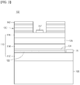
- FIG. 1 is a sectional view illustrating a light emitting diode 100 according to a first illustrative example
- FIG. 2 is a partially enlarged view illustrating a nitride semiconductor layer 130 of the light emitting diode 100 according to the first illustrative example.
- the light emitting diode 100 may include a substrate 105, a first conductivity type (abbreviated in the rest of the description: first conductive) semiconductor layer 112 on the substrate 150, an active layer 114 on the first conductive semiconductor layer 112, a second conductivity type (abbreviated in the rest of the description: second conductive) semiconductor layer 112 on the active layer 114, and a nitride semiconductor layer 130 having a refractive index less than that of the second conductive semiconductor layer 116 on the second conductive semiconductor layer 116.
- first conductivity type abbreviated in the rest of the description: first conductive
- second conductive abbreviated in the rest of the description: second conductive
- the nitride semiconductor layer 130 may include Al x Ga 1-x N (0 ⁇ x ⁇ 1).
- the present disclosure provides a light emitting diode, a method of manufacturing the same, a light emitting diode package, and a lighting system capable of improving light extraction efficiency.
- the present disclosure also provides a light emitting diode, a method of manufacturing the same, a light emitting diode package, and a lighting system capable of improving optical efficiency.
- a material having a low refractive index is grown in-situ during the growth of a light emitting diode (LED) to improve the light extraction efficiency.
- the refractive index n of the nitride semiconductor layer 130 may become gradually reduced from the active layer 114 to the second conductive semiconductor layer 116.
- the nitride semiconductor layer 130 may make contact with the second conductive semiconductor layer 116.
- the first illustrative example may control the refractive index of the nitride semiconductor layer by controlling a composition of A1 contained in the nitride semiconductor layer 130.
- the composition x of A1 contained in the nitride semiconductor layer 130 may become gradually increased from the active layer 114 to the second conductive semiconductor layer 116.
- the refractive index n of the nitride semiconductor layer 130 may become gradually reduced from the active layer 114 to the second conductive semiconductor layer 116 so that the light extraction efficiency of the light emitted from the active layer 114 may be increased in the upward direction rather than the lateral direction.
- the nitride semiconductor layer 130 may include a first nitride semiconductor layer 131, a second nitride semiconductor layer 132, a third nitride semiconductor layer 133, a fourth nitride semiconductor layer 134, a fifth nitride semiconductor layer 135, a sixth nitride semiconductor layer 136, a seventh nitride semiconductor layer 137, an eighth nitride semiconductor layer 138, and a ninth nitride semiconductor layer 139
- the first nitride semiconductor layer 131 may include GaN
- the ninth nitride semiconductor layer 139 may include AlN, but the first illustrative example is not limited thereto.
- the refractive index n of the nitride semiconductor layer 130 may become gradually reduced from the active layer 114 to the second conductive semiconductor layer 116 from about 2.4 to about 2.0, but the first illustrative example is not limited thereto.
- the nitride semiconductor layer 130 may include an n type nitride semiconductor layer doped with n type dopant.
- the nitride semiconductor layer 130 may be doped with Si, but the present disclosure is not limited thereto.
- nitride semiconductor layer 130 is doped with an n type dopant, even if a second electrode 152 is formed on the nitride semiconductor layer 130 without making contact with the second conductive semiconductor layer 116, a carrier may be easily injected.
- the nitride semiconductor layer 130 may have a thickness sufficient for enabling the tunneling of a carrier, but the first illustrative example is not limited thereto.
- the first illustrative example may further include a transmissive ohmic layer 140 having a refractive index less than that of the nitride semiconductor layer 130 on the nitride semiconductor layer 130.
- the second electrode 152 may be formed on the transmissive ohmic layer 140.
- a horizontal width of the first transmissive ohmic layer 140 may be substantially the same as a horizontal width of the nitride semiconductor layer 130 so that uniform current spreading may be achieved at the nitride semiconductor layer 130. Meanwhile, the horizontal width of the first transmissive ohmic layer 140 may be less than the horizontal width of the nitride semiconductor layer 130.
- the transmissive ohmic layer 140 may have a single or multi-layer structure of metal oxide capable of facilitating the carrier injection.
- the transmissive ohmic layer 140 may include at least one selected from the group consisting of ITO(indium tin oxide), IZO(indium zinc oxide), IZTO(indium zinc tin oxide), IAZO(indium aluminum zinc oxide), IGZO(indium gallium zinc oxide), IGTO(indium gallium tin oxide), AZO(aluminum zinc oxide), ATO(antimony tin oxide), GZO(gallium zinc oxide), IZON(IZO Nitride), AGZO(Al-Ga ZnO), IGZO(In-Ga ZnO), ZnO, IrOx, RuOx, NiO, RuOx/ITO, Ni/IrOx/Au, and Ni/IrOx/Au/ITO, and the present disclosure is not limited thereto.
- the refractive index n of the nitride semiconductor layer 130 may become gradually reduced from the active layer 114 to the second conductive semiconductor layer 116 from about 2.4 to about 2.0.
- the refractive index is controlled from about 2.0 to about over 1.0 in the transmissive ohmic layer 140, the refractive index becomes gradually reduced in the direction of the second conductive semiconductor layer 116, the nitride semiconductor layer 130, and the transmissive ohmic layer 140 so that light emitted from the active layer 114 may be efficiently extracted in the upward direction.
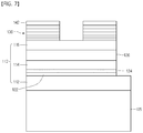
- FIG. 3 is a sectional view illustrating a light emitting diode 102 according to a second illustrative example.
- the second example may adopt the technical features and effects of the first example.
- the second electrode 152 may make contact with the second conductive semiconductor layer 116 through the nitride semiconductor layer 130.
- the thickness of the nitride semiconductor layer 130 for the tunneling of the carrier there is no limitation in the thickness of the nitride semiconductor layer 130 for the tunneling of the carrier.
- the nitride semiconductor layer 130 may include a p type nitride semiconductor layer doped with a p type element.
- the nitride semiconductor layer 130 including a p type nitride semiconductor layer doped with a p type element may be formed in-situ.
- the nitride semiconductor layer 130 may include an undoped nitride semiconductor layer which is not doped with an element. Upon the formation of the nitride semiconductor layer 130, a process may be performed without doping an n or p type conductive element to form the nitride semiconductor layer 130 including the undoped nitride semiconductor layer.
- the second illustrative example may further include a transparent insulating layer having a refractive index less than that of the nitride semiconductor layer 130 on the nitride semiconductor layer 130.
- the transparent insulating layer 142 may include silicon oxide or silicon nitride, but the present example is not limited thereto.
- the refractive index n of the nitride semiconductor layer 130 may become gradually reduced from the active layer 114 to the second conductive semiconductor layer 116 from about 2.4 to about 2.0, and the refractive index becomes gradually reduced in the direction of the second conductive semiconductor layer 116, the nitride semiconductor layer 130, and the transparent insulating layer 142 by controlling the refractive index of the transparent insulating layer 142 from about 2.0 to about over 1.0 so that light emitted from the active layer 114 may be more efficiently extracted in the upward direction rather than the lateral direction.
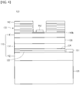
- FIG. 4 is a sectional view illustrating a light emitting diode 103 according to an embodiment of the present invention.
- the present third embodiment may adopt the technical features and effects of the first and second illustrative examples.
- the present embodiment includes further a light transmissive ohmic layer 140b between the second conductive semiconductor layer 116 and the nitride semiconductor layer 130.
- the light transmissive ohmic layer 140b has a refractive index between the refractive index of the second conductive layer 116 and the refractive index of the nitride semiconductor layer 130 so that light extraction efficiency may be maximized.
- the second electrode 152 formed above the second conductive semiconductor layer 116 may be formed on the light transmissive ohmic layer 140b.
- spreading of light may be improved and the present disclosure is easily applied to a product by controlling the content (%) of Al.
- light extraction efficiency can be increased. Further, according to the present disclosure, optical efficiency can be increased.
- the substrate 105 as shown in FIG. 5 may be prepared.
- the substrate 105 may include a conductive substrate or an insulating substrate.
- the substrate 105 may include at least one of Al 2 O 3 , SiC, Si, GaAs, GaN, ZnO, GaP, InP, Ge, and Ga 2 O 3 .
- a concave-convex structure can be formed on the substrate 105, but the present disclosure is not limited thereto.
- the substrate 105 can be subject to the wet cleaning to remove impurities from the surface of the substrate 105.
- a light extraction structure for example, a PSS (not shown) may be formed on the substrate 105, but the present disclosure is not limited thereto.
- the light emitting structure 110 including the first conductive semiconductor layer 112, the active layer 114 and the second semiconductor layer 116 may be formed on the substrate 105.
- a buffer layer (not shown) may be formed on the substrate 105.
- the buffer layer may attenuate lattice mismatch between the light emitting structure 110 and the substrate 105.
- the buffer layer may include the group III-V compound semiconductor.
- the buffer layer may include at least one of GaN, InN, AlN, InGaN, AlGaN, InAlGaN, and AlInN.
- An undoped semiconductor layer (not shown) may be formed on the buffer layer, but the present disclosure is not limited thereto.
- a first conductive layer 112 may be formed on the substrate 105 or the semiconductor layer.
- the first conductive semiconductor layer 112 may include a group III-V compound semiconductor doped with a first conductive dopant. If the first conductive semiconductor layer 112 is an N type semiconductor layer, the first conductive dopant is an N type dopant, such as Si, Ge, Sn, Se, or Te, but the present disclosure is not limited thereto.
- the first conductive semiconductor layer 122 may include semiconductor material having the compositional formula of In x Al y Ga 1-x-y N (0 ⁇ x ⁇ 1, 0 ⁇ y ⁇ 1, 0 ⁇ x+y ⁇ 1).
- the first conductive semiconductor layer 112 may include at least one of GaN, InN, AlN, InGaN, AlGaN, InAlGaN, AlInN, AlGaAs, InGaAs, AlInGaAs, GaP, AlGaP, InGaP, AlInGaP, and InP.
- the first conductive semiconductor layer 112 may include an N type GaN layer, which is formed through the CVD, MBE, sputtering or HVPE.
- the first conductive semiconductor layer 112 may be formed by injecting trimethyl gallium (TMGa) gas, ammonia (NH 3 ) gas, nitrogen (N 2 ) gas and silane (SiH 4 ) gas including n type impurities, such as silicon, into the chamber.
- TMGa trimethyl gallium
- NH 3 ammonia
- N 2 nitrogen
- SiH 4 silane
- a current spreading layer 122 may be formed on the first conductive semiconductor layer 112.
- the current spreading layer 122 may be an undoped GaN layer, but the present disclosure is not limited thereto.
- an electron injection layer 124 may be formed on the current spreading layer 122.
- the electron injection layer 124 may be a first conductive GaN layer. Electrons may be effectively injected into the electron injection layer 124 by doping the electron injection layer 124 with an N type doping element at a concentration of 6.0x10 18 atoms/cm 3 ⁇ 8.0x10 18 atoms/cm 3 .
- a strain control layer (not shown) may be formed on the electron injection layer 124.
- a strain control layer including In y Al x Ga (1-x-y) N (0 ⁇ x ⁇ 1, 0 ⁇ y ⁇ 1)/GaN may be formed on the electron injection layer 124.
- the strain control layer may efficiently attenuate the stress resulting from lattice mismatch between the first conductive semiconductor layer 112 and the active layer 114.
- the strain control layer is repeatedly laminated in at least 6 periods having the compositional formula of a first In x1 GaN and a second In x2 GaN, more electrons are collected at a low energy level of the active layer 114 so that a recombination probability of electrons and holes is increased, thereby improving light emission efficiency.
- the active layer 114 may be formed on the first conductive semiconductor layer 112.
- the active layer 114 may include at least one of a single quantum well structure, a multiple quantum well (MQW) structure, a quantum wire structure and a quantum dot structure.
- MQW multiple quantum well
- the active layer 114 can be formed with the MQW structure by injecting TMGa gas, NH 3 gas, N 2 gas, and trimethyl indium (TMIn) gas, but the present disclosure is not limited thereto.
- the active layer 114 may have a well/barrier layer including at least one of InGaN/GaN, InGaN/InGaN, AlGaN/GaN, InAlGaN/GaN, GaAs/AlGaAs (InGaAs) and GaP/AlGaP (InGaP), but the present disclosure is not limited thereto.
- the well layer may include material having the bandgap energy lower than that of the barrier layer.
- an electron blocking layer 126 may be formed on the active layer 114 for the purpose of electron blocking and MQW cladding of an active layer so that light emitting efficiency may be improved.
- the electron blocking layer 126 may include an Al x In y Ga (1-x-y) N (0 ⁇ x ⁇ 1,0 ⁇ y ⁇ 1)-based semiconductor having the energy bandgap higher than that of the active layer 114.
- the electron blocking layer 126 may have a thickness in the range of about 100 ⁇ to about 600 ⁇ , but the present disclosure is not limited thereto.
- the electron blocking layer 126 may have an Al z Ga (1-z) N/GaN (0 ⁇ z ⁇ 1) super lattice, but the present disclosure is not limited thereto.
- a p type ion may be implanted into the electron blocking layer 126 to efficiently block overflow of electrons and increase injection efficiency of holes.
- An Mg ion is implanted into the electron blocking layer 126 at the concentration in the range of about 10 18 / cm 3 to about 10 20 /cm 3 to efficiently block overflow electrons and increase injection efficiency of holes.
- a second conductive semiconductor layer 116 may be formed on the electron blocking layer 126.
- the second conductive semiconductor layer 116 may include the group III-V compound semiconductor doped with the second conductive dopant.
- the second conductive semiconductor layer 116 may include the semiconductor material having the compositional formula of In x Al y Ga 1-x-y N (0 ⁇ x ⁇ 1, 0 ⁇ y ⁇ 1, 0 ⁇ x+y ⁇ 1).
- the second conductive semiconductor layer 126 may include one selected from the group consisting of GaN, AlN, AlGaN, InGaN, InN, InAlGaN, AlInN, AlGaAs, GaP, GaAs, GaAsP, and AlGaInP.
- the second conductive dopant includes the P type dopant such as Mg, Zn, Ca, Sr, or Ba.
- the second conductive semiconductor layer 126 can be prepared as a single layer or a multiple layer, but the present disclosure is not limited thereto.
- the second conductive semiconductor layer 116 may include a p type GaN layer, which can be formed by injecting TMGa gas, NH 3 gas, N 2 gas and (EtCp 2 Mg) ⁇ Mg(C 2 H 5 C 5 H 4 ) 2 ⁇ gas including p type impurities (for example, Mg) into the chamber, but the present disclosure is not limited thereto.
- the first conductive semiconductor layer 112 may include an N type semiconductor layer and the second conductive semiconductor layer 126 may include a P type semiconductor layer, but the present disclosure is not limited thereto.
- a semiconductor layer such as an N type semiconductor layer (not shown) having polarity opposite to that of the second conductive semiconductor layer 126, can be formed on the second conductive semiconductor layer 126.
- the light emitting structure 110 may include one of an N-P junction structure, a P-N junction structure, an N-P-N junction structure, and a P-N-P junction structure.
- nitride semiconductor layer 130 having a refractive index less than that of the second conductive semiconductor layer 116 is formed on the second conductive semiconductor layer 116.
- the nitride semiconductor layer 130 may include AlxGa 1-x N (0 ⁇ x ⁇ 1).
- Light extraction efficiency may be improved by growing a material of a low refractive index in-situ during the growth of a light emitting diode (LED).
- the refractive index n of the nitride semiconductor layer 130 may become gradually reduced from the active layer 114 to the second conductive semiconductor layer 116.
- the present disclosure may control the refractive index of the nitride semiconductor layer by controlling a composition of Al contained in the nitride semiconductor layer 130.
- the composition x of Al contained in the nitride semiconductor layer 130 may become gradually increased from the active layer 114 to the second conductive semiconductor layer 116.
- the refractive index n of the nitride semiconductor layer 130 may become gradually reduced from the active layer 114 to the second conductive semiconductor layer 116 so that light emitted from the active layer 114 may increase light extraction efficiency in the upward direction rather than the lateral direction.
- the refractive index n of the nitride semiconductor layer 130 may become gradually reduced from the active layer 114 to the second conductive semiconductor layer 116 from about 2.4 to about 2.0, but the present disclosure is not limited thereto.
- the nitride semiconductor layer 130 may include an N type nitride semiconductor layer doped with an N type dopant.
- the nitride semiconductor layer 130 may be doped with Si, but the present disclosure is not limited thereto.
- the nitride semiconductor layer 130 is doped with an N type dopant, even if a second electrode 152 is formed on the nitride semiconductor layer 130 without making contact with the second conductive semiconductor layer 116, a carrier may be easily injected.
- the nitride semiconductor layer 130 may have a thickness sufficient for enabling the tunneling of a carrier, but the present disclosure is not limited thereto.
- the first illustrative example may further include a transmissive ohmic layer 140 having a refractive index less than that of the nitride semiconductor layer 130 on the nitride semiconductor layer 130.
- the second electrode 152 may be formed on the transmissive ohmic layer 140.
- the transmissive ohmic layer 140 may have a single or multi-layer structure of metal oxide capable of facilitating the carrier injection.
- the transmissive ohmic layer 140 may include at least one selected from the group consisting of ITO(indium tin oxide), IZO(indium zinc oxide), IZTO(indium zinc tin oxide), IAZO(indium aluminum zinc oxide), IGZO(indium gallium zinc oxide), IGTO(indium gallium tin oxide), AZO(aluminum zinc oxide), ATO(antimony tin oxide), GZO(gallium zinc oxide), IZON(IZO Nitride), AGZO(Al-Ga ZnO), IGZO(In-Ga ZnO), ZnO, IrOx, RuOx, NiO, RuOx/ITO, Ni/IrOx/Au, and Ni/IrOx/Au/ITO, and the present disclosure is not limited thereto.
- the refractive index n of the nitride semiconductor layer 130 may become gradually reduced from the active layer 114 to the second conductive semiconductor layer 116 from about 2.4 to about 2.0. Since the refractive index is controlled from about 2.0 to about over 1.0 in the transmissive ohmic layer 140, the refractive index becomes gradually reduced in the direction of the second conductive semiconductor layer 116, the nitride semiconductor layer 130, and the transmissive ohmic layer 140 so that light emitted from the active layer 114 may be efficiently extracted in the upward direction.
- the second illustrative example may further include a transparent insulating layer 142 having a refractive index less than that of the nitride semiconductor layer 130 on the nitride semiconductor layer.
- the transparent insulating layer 142 may include silicon oxide or silicon nitride, but the present disclosure is not limited thereto.
- the refractive index n of the nitride semiconductor layer 130 may become gradually reduced from the active layer 114 to the second conductive semiconductor layer 116 from about 2.4 to about 2.0. Since the refractive index is controlled from about 2.0 to about over 1.0 in the transmissive ohmic layer 140, the refractive index becomes gradually reduced in the direction of the second conductive semiconductor layer 116, the nitride semiconductor layer 130, and the transmissive ohmic layer 140 so that light emitted from the active layer 114 may be efficiently extracted in the upward direction.
- the second electrode 152 may make contact with the second conductive semiconductor layer 116 through the nitride semiconductor layer 130.
- the embodiment of the present invention further includes a light transmissive ohmic layer 140b between the second conductive semiconductor layer 116 and the nitride semiconductor layer 130.
- the light transmissive ohmic layer 140b has a refractive index between the refractive index of the second conductive layer 116 and the refractive index of the nitride semiconductor layer 130 so that light extraction efficiency may be maximized.
- spreading of light may be improved and the embodiment of the present invention is easily applied to a product by controlling the content (%) of Al.
- the second conductive semiconductor layer 116 may be exposed by partially removing the transparent insulating layer 142 and the nitride semiconductor layer 130.
- the first conductive semiconductor layer 112 may be exposed by partially removing the transparent insulating layer 142, the nitride semiconductor layer 130, the second conductive semiconductor layer, the electron blocking layer, a strain control layer, and the electron injection layer 124, and the current spreading layer 122.
- a second electrode 152 and a first electrode 151 may be formed on the second exposed conductive semiconductor layer 116 and the first exposed conductive semiconductor layer 112, respectively.
- light extraction efficiency can be increased.
- optical efficiency can be increased.
- FIG. 9 is a sectional view illustrating a light emitting diode package 200 according to the present disclosure.
- the light emitting diode package 200 includes a package body 205, third and fourth electrode layers 213 and 214 formed on the package body 205, the light emitting diode 100 provided on the package body 205 and electrically connected to the third and fourth electrode layers 213 and 214, and a molding member 240 that surrounds the light emitting diode 100.
- the package body 205 may include silicon, synthetic resin or metallic material.
- An inclined surface may be formed around the light emitting diode 100.
- the third and fourth electrode layers 213 and 214 may be electrically isolated from each other to supply power to the light emitting diode 100.
- the third and fourth electrode layers 213 and 214 reflect the light emitted from the light emitting diode 100 to improve the light efficiency and dissipate heat generated from the light emitting diode 100 to the outside.
- the lateral type light emitting diode shown in FIG. 1 , 3 , or 4 can be employed as the light emitting diode 100, but the present disclosure is not limited thereto.
- the light emitting diode 100 may be installed on the package body 205 or the third and fourth electrode layers 213 and 214.
- the light emitting diode 100 is electrically connected to the third electrode layer 213 and/or the fourth electrode layer 214 through at least one of a wire bonding scheme, a flip chip bonding scheme and a die bonding scheme. According to the present disclosure, the light emitting diode 100 is electrically connected to the third electrode layer 213 through a wire and electrically connected to the fourth electrode layer 214 through the die bonding scheme, but the present disclosure is not limited thereto.
- the molding member 230 surrounds the light emitting diode 100 to protect the light emitting diode 100.
- the molding member 230 may include phosphors to change the wavelength of the light emitted from the light emitting diode 100.
- a plurality of light emitting diode packages according to the present disclosure may be arrayed on a substrate, and an optical member including a light guide plate, a prism sheet, a diffusion sheet or a fluorescent sheet may be provided on the optical path of the light emitted from the light emitting diode package.
- the light emitting diode package, the substrate, and the optical member may serve as a backlight unit or a lighting unit.
- the lighting system may include a backlight unit, a lighting unit, an indicator, a lamp or a streetlamp.
- FIG. 10 is an exploded perspective view an example of a lighting system including the light emitting diode according to the present disclosure.
- the lighting system according to the present disclosure may include a cover 2100, a light source module 2200, a radiator 2400, a power supply part 2600, an inner case 2700, and a socket 2800.
- the lighting system according to the present disclosure may further include at least one of a member 2300 and a holder 2500.
- the light source module 2200 may include the light emitting diode 100 or the light emitting diode package 200 according to the present disclosure.
- the cover 2100 may have a bulb shape, a hemisphere shape, a partially-open hollow shape.
- the cover 2100 may be optically coupled with the light source module 2200.
- the cover 2100 may diffuse, scatter, or excite light provided from the light source module.
- the cover 2100 may be a type of optical member.
- the cover 2100 may be coupled with the radiator 2400.
- the cover 2100 may include a coupling part which is coupled with the radiator 2400.
- the cover 2100 may include an inner surface coated with a milk-white paint.
- the milk-white paint may include a diffusion material to diffuse light.
- the cover 2100 may have the inner surface of which surface roughness is greater than that of the outer surface thereof. The surface roughness is provided for the purpose of sufficiently scattering and diffusing the light from the light source module 2200.
- a material of the cover 2100 may include glass, plastic, polypropylene (PP), polyethylene (PE), and polycarbonate (PC).
- the polycarbonate (PC) has the superior light resistance, heat resistance and strength among the above materials.
- the cover 2100 may be transparent so that a user may view the light source module 2200 from the outside, or opaque.
- the cover 2100 may be formed through a blow molding scheme.
- the light source module 2200 may be disposed at one surface of the radiator 2400. Accordingly, the heat from the light source module 2200 is transferred to the radiator 2400.
- the light source module 2200 may include a light source 2210, a connection plate 2230, and a connector 2250.
- the member 2300 is disposed at a top surface of the radiator 2400, and includes guide grooves 2310 into which a plurality of light sources 2210 and the connector 2250 are inserted.
- the guide grooves 2310 correspond to a substrate of the light source 2210 and the connector 2250.
- a surface of the member 2300 may be coated with a light reflective material.
- the surface of the member 2300 may be coated with white paint.
- the member 2300 again reflects light, which is reflected by the inner surface of the cover 2100 and is returned to the direction of the light source module 2200, to the direction of the cover 2100. Accordingly, the light efficiency of the lighting system according to the present disclosure may be improved.
- the member 2300 may include an insulating material.
- the connection plate 2230 of the light source module 2200 may include an electrically conductive material.
- the radiator 2400 may be electrically connected to the connection plate 2230.
- the member 2300 may be configured by an insulating material, thereby preventing the connection plate 2230 from being electrically shorted with the radiator 2400.
- the radiator 2400 receives heat from the light source module 2200 and the power supply part 2600 and radiates the heat.
- the holder 2500 covers a receiving groove 2719 of an insulating part 2710 of an inner case 2700. Accordingly, the power supply part 2600 received in the insulating part 2710 of the inner case 2700 is closed.
- the holder 2500 includes a guide protrusion 2510.
- the guide protrusion 2510 has a hole through a protrusion of the power supply part 2600.
- the power supply part 2600 processes or converts an electric signal received from the outside and provides the processed or converted electric signal to the light source module 2200.
- the power supply part 2600 is received in the receiving groove of the inner case 2700, and is closed inside the inner case 2700 by the holder 2500.
- the power supply part 2600 may include a protrusion 2610, a guide part 2630, a base 2650, and an extension part 2670.
- the guide part 2630 has a shape protruding from one side of the base 2650 to the outside.
- the guide part 2630 may be inserted into the holder 2500.
- a plurality of components may be disposed above one surface of the base 2650.
- the components may include a DC converter converting AC power provided from an external power supply into DC power, a driving chip controlling driving of the light source module 2200, and an electrostatic discharge (ESD) protection device protecting the light source module 2200, but the present disclosure is not limited thereto.
- the extension part 2670 has a shape protruding from an opposite side of the base 2650 to the outside.
- the extension part 2670 is inserted into an inside of the connection part 2750 of the inner case 2700, and receives an electric signal from the outside.
- a width of the extension part 2670 may be smaller than or equal to a width of the connection part 2750 of the inner case 2700.
- First terminals of a "+ electric wire” and a "- electric wire” are electrically connected to the extension part 2670 and second terminals of the "+ electric wire” and the "- electric wire” may be electrically connected to a socket 2800.
- the inner case 2700 may include a molding part therein together with the power supply part 2600.
- the molding part is prepared by hardening molding liquid, and the power supply part 2600 may be fixed inside the inner case 2700 by the molding part.
- the light extraction efficiency can be increased.
- the optical efficiency can be increased.
Landscapes
- Engineering & Computer Science (AREA)
- Architecture (AREA)
- Mechanical Engineering (AREA)
- Civil Engineering (AREA)
- Structural Engineering (AREA)
- Health & Medical Sciences (AREA)
- General Health & Medical Sciences (AREA)
- Business, Economics & Management (AREA)
- Emergency Management (AREA)
- Led Devices (AREA)
- Non-Portable Lighting Devices Or Systems Thereof (AREA)
- Led Device Packages (AREA)
Applications Claiming Priority (1)
| Application Number | Priority Date | Filing Date | Title |
|---|---|---|---|
| KR20120000622A KR20130079873A (ko) | 2012-01-03 | 2012-01-03 | 발광소자 및 이를 포함하는 조명시스템 |
Publications (3)
| Publication Number | Publication Date |
|---|---|
| EP2613368A2 EP2613368A2 (en) | 2013-07-10 |
| EP2613368A3 EP2613368A3 (en) | 2016-02-17 |
| EP2613368B1 true EP2613368B1 (en) | 2020-05-06 |
Family
ID=47428533
Family Applications (1)
| Application Number | Title | Priority Date | Filing Date |
|---|---|---|---|
| EP13150060.5A Not-in-force EP2613368B1 (en) | 2012-01-03 | 2013-01-02 | Light emitting diode |
Country Status (6)
| Country | Link |
|---|---|
| US (1) | US9018652B2 (https=) |
| EP (1) | EP2613368B1 (https=) |
| JP (1) | JP6087142B2 (https=) |
| KR (1) | KR20130079873A (https=) |
| CN (1) | CN103187496B (https=) |
| TW (1) | TWI596798B (https=) |
Families Citing this family (3)
| Publication number | Priority date | Publication date | Assignee | Title |
|---|---|---|---|---|
| TWI758603B (zh) * | 2014-07-03 | 2022-03-21 | 晶元光電股份有限公司 | 光電元件及其製造方法 |
| CN105224120B (zh) * | 2014-07-03 | 2018-07-31 | 宸鸿科技(厦门)有限公司 | 基板结构 |
| TWI759602B (zh) * | 2019-05-24 | 2022-04-01 | 晶元光電股份有限公司 | 半導體元件 |
Family Cites Families (25)
| Publication number | Priority date | Publication date | Assignee | Title |
|---|---|---|---|---|
| JPH09116192A (ja) * | 1995-10-16 | 1997-05-02 | Toshiba Corp | 発光ダイオード |
| CN100446289C (zh) * | 1998-03-12 | 2008-12-24 | 日亚化学工业株式会社 | 氮化物半导体元件 |
| JP4356555B2 (ja) * | 1998-03-12 | 2009-11-04 | 日亜化学工業株式会社 | 窒化物半導体素子 |
| KR100589621B1 (ko) * | 1998-03-12 | 2006-06-19 | 니치아 카가쿠 고교 가부시키가이샤 | 질화물 반도체 소자 |
| JP3804335B2 (ja) * | 1998-11-26 | 2006-08-02 | ソニー株式会社 | 半導体レーザ |
| WO2002084829A1 (en) * | 2001-04-11 | 2002-10-24 | Cielo Communications, Inc. | Long wavelength vertical cavity surface emitting laser |
| US7692182B2 (en) * | 2001-05-30 | 2010-04-06 | Cree, Inc. | Group III nitride based quantum well light emitting device structures with an indium containing capping structure |
| TW493287B (en) * | 2001-05-30 | 2002-07-01 | Epistar Corp | Light emitting diode structure with non-conductive substrate |
| JP2003168822A (ja) * | 2001-11-30 | 2003-06-13 | Shin Etsu Handotai Co Ltd | 発光素子及びその製造方法 |
| JP4254373B2 (ja) * | 2003-06-24 | 2009-04-15 | 日亜化学工業株式会社 | 窒化物半導体素子 |
| US7751455B2 (en) * | 2004-12-14 | 2010-07-06 | Palo Alto Research Center Incorporated | Blue and green laser diodes with gallium nitride or indium gallium nitride cladding laser structure |
| JP2007096116A (ja) * | 2005-09-29 | 2007-04-12 | Toyoda Gosei Co Ltd | 発光素子 |
| JP2007134388A (ja) * | 2005-11-08 | 2007-05-31 | Sharp Corp | 窒化物系半導体素子とその製造方法 |
| JP2007220973A (ja) * | 2006-02-17 | 2007-08-30 | Showa Denko Kk | 半導体発光素子及びその製造方法、並びにランプ |
| US20070228385A1 (en) * | 2006-04-03 | 2007-10-04 | General Electric Company | Edge-emitting light emitting diodes and methods of making the same |
| TW200812113A (en) * | 2006-05-23 | 2008-03-01 | Alps Electric Co Ltd | Semiconductor light emitting element and method for manufacturing the same |
| EP1883141B1 (de) * | 2006-07-27 | 2017-05-24 | OSRAM Opto Semiconductors GmbH | LD oder LED mit Übergitter-Mantelschicht |
| US8158990B2 (en) * | 2006-10-05 | 2012-04-17 | Mitsubishi Chemical Corporation | Light emitting device using GaN LED chip |
| US20080277682A1 (en) * | 2007-03-29 | 2008-11-13 | The Regents Of The University Of California | Dual surface-roughened n-face high-brightness led |
| JP2009038239A (ja) * | 2007-08-02 | 2009-02-19 | Toshiba Corp | 光半導体装置 |
| JP5164641B2 (ja) * | 2008-04-02 | 2013-03-21 | Dowaエレクトロニクス株式会社 | 電流狭窄型半導体発光素子の製造方法 |
| KR101072200B1 (ko) * | 2009-03-16 | 2011-10-10 | 엘지이노텍 주식회사 | 발광소자 및 그 제조방법 |
| KR101028286B1 (ko) * | 2009-12-28 | 2011-04-11 | 엘지이노텍 주식회사 | 반도체 발광소자 및 그 제조방법 |
| JP5994420B2 (ja) * | 2012-06-21 | 2016-09-21 | 豊田合成株式会社 | Iii族窒化物半導体発光素子およびその製造方法 |
| US20140097442A1 (en) * | 2012-10-09 | 2014-04-10 | Industrial Technology Research Institute | Nitride semiconductor device |
-
2012
- 2012-01-03 KR KR20120000622A patent/KR20130079873A/ko not_active Ceased
- 2012-12-27 TW TW101150516A patent/TWI596798B/zh not_active IP Right Cessation
- 2012-12-28 JP JP2012287333A patent/JP6087142B2/ja not_active Expired - Fee Related
- 2012-12-31 CN CN201210593041.7A patent/CN103187496B/zh not_active Expired - Fee Related
-
2013
- 2013-01-02 US US13/732,694 patent/US9018652B2/en active Active
- 2013-01-02 EP EP13150060.5A patent/EP2613368B1/en not_active Not-in-force
Non-Patent Citations (1)
| Title |
|---|
| None * |
Also Published As
| Publication number | Publication date |
|---|---|
| TW201340386A (zh) | 2013-10-01 |
| EP2613368A3 (en) | 2016-02-17 |
| US20130168711A1 (en) | 2013-07-04 |
| KR20130079873A (ko) | 2013-07-11 |
| JP6087142B2 (ja) | 2017-03-01 |
| JP2013140983A (ja) | 2013-07-18 |
| TWI596798B (zh) | 2017-08-21 |
| CN103187496A (zh) | 2013-07-03 |
| EP2613368A2 (en) | 2013-07-10 |
| CN103187496B (zh) | 2017-05-31 |
| US9018652B2 (en) | 2015-04-28 |
Similar Documents
| Publication | Publication Date | Title |
|---|---|---|
| EP2908352B1 (en) | Light-emitting device | |
| EP2482343A2 (en) | Light emitting diode | |
| EP2814069B1 (en) | Multiple quantum well semiconductor light emitting device | |
| KR102328457B1 (ko) | 발광소자, 발광소자 제조방법 및 이를 구비하는 조명시스템 | |
| KR101894025B1 (ko) | 발광소자 | |
| KR20140145739A (ko) | 발광소자 | |
| KR20120138275A (ko) | 발광소자 | |
| EP2613368B1 (en) | Light emitting diode | |
| KR101956048B1 (ko) | 발광소자 | |
| EP2816616B1 (en) | Light emitting device and lighting system | |
| KR101786084B1 (ko) | 발광소자의 제조방법 | |
| KR101886153B1 (ko) | 발광소자 | |
| KR102057719B1 (ko) | 발광소자 및 이를 포함하는 조명시스템 | |
| KR101871498B1 (ko) | 발광소자 | |
| KR20150089816A (ko) | 발광소자 및 이를 구비하는 조명 시스템 | |
| KR102042263B1 (ko) | 발광소자 및 이를 구비하는 조명 시스템 | |
| KR102181482B1 (ko) | 발광소자 및 조명시스템 | |
| KR101969336B1 (ko) | 발광소자 | |
| KR20150006631A (ko) | 발광소자 및 조명시스템 | |
| KR20140062947A (ko) | 발광소자 | |
| KR20120015882A (ko) | 발광소자 패키지 | |
| KR20130035402A (ko) | 발광소자 및 발광소자의 제조방법 | |
| KR20130014195A (ko) | 발광소자 및 발광소자 패키지 |
Legal Events
| Date | Code | Title | Description |
|---|---|---|---|
| PUAI | Public reference made under article 153(3) epc to a published international application that has entered the european phase |
Free format text: ORIGINAL CODE: 0009012 |
|
| AK | Designated contracting states |
Kind code of ref document: A2 Designated state(s): AL AT BE BG CH CY CZ DE DK EE ES FI FR GB GR HR HU IE IS IT LI LT LU LV MC MK MT NL NO PL PT RO RS SE SI SK SM TR |
|
| AX | Request for extension of the european patent |
Extension state: BA ME |
|
| 17P | Request for examination filed |
Effective date: 20140331 |
|
| RBV | Designated contracting states (corrected) |
Designated state(s): AL AT BE BG CH CY CZ DE DK EE ES FI FR GB GR HR HU IE IS IT LI LT LU LV MC MK MT NL NO PL PT RO RS SE SI SK SM TR |
|
| PUAL | Search report despatched |
Free format text: ORIGINAL CODE: 0009013 |
|
| AK | Designated contracting states |
Kind code of ref document: A3 Designated state(s): AL AT BE BG CH CY CZ DE DK EE ES FI FR GB GR HR HU IE IS IT LI LT LU LV MC MK MT NL NO PL PT RO RS SE SI SK SM TR |
|
| AX | Request for extension of the european patent |
Extension state: BA ME |
|
| RIC1 | Information provided on ipc code assigned before grant |
Ipc: H01L 33/04 20100101ALN20160111BHEP Ipc: H01L 33/32 20100101AFI20160111BHEP Ipc: H01L 33/20 20100101ALN20160111BHEP Ipc: H01L 33/44 20100101ALN20160111BHEP Ipc: H01L 33/42 20100101ALN20160111BHEP |
|
| RAP1 | Party data changed (applicant data changed or rights of an application transferred) |
Owner name: LG INNOTEK CO., LTD. |
|
| GRAP | Despatch of communication of intention to grant a patent |
Free format text: ORIGINAL CODE: EPIDOSNIGR1 |
|
| STAA | Information on the status of an ep patent application or granted ep patent |
Free format text: STATUS: GRANT OF PATENT IS INTENDED |
|
| RIC1 | Information provided on ipc code assigned before grant |
Ipc: F21Y 115/10 20160101ALN20191211BHEP Ipc: F21K 9/23 20160101ALN20191211BHEP Ipc: H01L 33/42 20100101ALI20191211BHEP Ipc: H01L 33/44 20100101ALN20191211BHEP Ipc: H01L 33/32 20100101AFI20191211BHEP Ipc: H01L 33/04 20100101ALN20191211BHEP Ipc: H01L 33/38 20100101ALN20191211BHEP Ipc: H01L 33/20 20100101ALN20191211BHEP |
|
| INTG | Intention to grant announced |
Effective date: 20200110 |
|
| GRAS | Grant fee paid |
Free format text: ORIGINAL CODE: EPIDOSNIGR3 |
|
| GRAA | (expected) grant |
Free format text: ORIGINAL CODE: 0009210 |
|
| STAA | Information on the status of an ep patent application or granted ep patent |
Free format text: STATUS: THE PATENT HAS BEEN GRANTED |
|
| AK | Designated contracting states |
Kind code of ref document: B1 Designated state(s): AL AT BE BG CH CY CZ DE DK EE ES FI FR GB GR HR HU IE IS IT LI LT LU LV MC MK MT NL NO PL PT RO RS SE SI SK SM TR |
|
| REG | Reference to a national code |
Ref country code: GB Ref legal event code: FG4D |
|
| REG | Reference to a national code |
Ref country code: AT Ref legal event code: REF Ref document number: 1268243 Country of ref document: AT Kind code of ref document: T Effective date: 20200515 Ref country code: CH Ref legal event code: EP |
|
| REG | Reference to a national code |
Ref country code: IE Ref legal event code: FG4D |
|
| REG | Reference to a national code |
Ref country code: DE Ref legal event code: R096 Ref document number: 602013068626 Country of ref document: DE |
|
| REG | Reference to a national code |
Ref country code: LT Ref legal event code: MG4D |
|
| REG | Reference to a national code |
Ref country code: NL Ref legal event code: MP Effective date: 20200506 |
|
| PG25 | Lapsed in a contracting state [announced via postgrant information from national office to epo] |
Ref country code: FI Free format text: LAPSE BECAUSE OF FAILURE TO SUBMIT A TRANSLATION OF THE DESCRIPTION OR TO PAY THE FEE WITHIN THE PRESCRIBED TIME-LIMIT Effective date: 20200506 Ref country code: PT Free format text: LAPSE BECAUSE OF FAILURE TO SUBMIT A TRANSLATION OF THE DESCRIPTION OR TO PAY THE FEE WITHIN THE PRESCRIBED TIME-LIMIT Effective date: 20200907 Ref country code: IS Free format text: LAPSE BECAUSE OF FAILURE TO SUBMIT A TRANSLATION OF THE DESCRIPTION OR TO PAY THE FEE WITHIN THE PRESCRIBED TIME-LIMIT Effective date: 20200906 Ref country code: GR Free format text: LAPSE BECAUSE OF FAILURE TO SUBMIT A TRANSLATION OF THE DESCRIPTION OR TO PAY THE FEE WITHIN THE PRESCRIBED TIME-LIMIT Effective date: 20200807 Ref country code: NO Free format text: LAPSE BECAUSE OF FAILURE TO SUBMIT A TRANSLATION OF THE DESCRIPTION OR TO PAY THE FEE WITHIN THE PRESCRIBED TIME-LIMIT Effective date: 20200806 Ref country code: LT Free format text: LAPSE BECAUSE OF FAILURE TO SUBMIT A TRANSLATION OF THE DESCRIPTION OR TO PAY THE FEE WITHIN THE PRESCRIBED TIME-LIMIT Effective date: 20200506 Ref country code: SE Free format text: LAPSE BECAUSE OF FAILURE TO SUBMIT A TRANSLATION OF THE DESCRIPTION OR TO PAY THE FEE WITHIN THE PRESCRIBED TIME-LIMIT Effective date: 20200506 |
|
| PG25 | Lapsed in a contracting state [announced via postgrant information from national office to epo] |
Ref country code: BG Free format text: LAPSE BECAUSE OF FAILURE TO SUBMIT A TRANSLATION OF THE DESCRIPTION OR TO PAY THE FEE WITHIN THE PRESCRIBED TIME-LIMIT Effective date: 20200806 Ref country code: HR Free format text: LAPSE BECAUSE OF FAILURE TO SUBMIT A TRANSLATION OF THE DESCRIPTION OR TO PAY THE FEE WITHIN THE PRESCRIBED TIME-LIMIT Effective date: 20200506 Ref country code: RS Free format text: LAPSE BECAUSE OF FAILURE TO SUBMIT A TRANSLATION OF THE DESCRIPTION OR TO PAY THE FEE WITHIN THE PRESCRIBED TIME-LIMIT Effective date: 20200506 Ref country code: LV Free format text: LAPSE BECAUSE OF FAILURE TO SUBMIT A TRANSLATION OF THE DESCRIPTION OR TO PAY THE FEE WITHIN THE PRESCRIBED TIME-LIMIT Effective date: 20200506 |
|
| REG | Reference to a national code |
Ref country code: AT Ref legal event code: MK05 Ref document number: 1268243 Country of ref document: AT Kind code of ref document: T Effective date: 20200506 |
|
| PG25 | Lapsed in a contracting state [announced via postgrant information from national office to epo] |
Ref country code: AL Free format text: LAPSE BECAUSE OF FAILURE TO SUBMIT A TRANSLATION OF THE DESCRIPTION OR TO PAY THE FEE WITHIN THE PRESCRIBED TIME-LIMIT Effective date: 20200506 Ref country code: NL Free format text: LAPSE BECAUSE OF FAILURE TO SUBMIT A TRANSLATION OF THE DESCRIPTION OR TO PAY THE FEE WITHIN THE PRESCRIBED TIME-LIMIT Effective date: 20200506 |
|
| PG25 | Lapsed in a contracting state [announced via postgrant information from national office to epo] |
Ref country code: SM Free format text: LAPSE BECAUSE OF FAILURE TO SUBMIT A TRANSLATION OF THE DESCRIPTION OR TO PAY THE FEE WITHIN THE PRESCRIBED TIME-LIMIT Effective date: 20200506 Ref country code: EE Free format text: LAPSE BECAUSE OF FAILURE TO SUBMIT A TRANSLATION OF THE DESCRIPTION OR TO PAY THE FEE WITHIN THE PRESCRIBED TIME-LIMIT Effective date: 20200506 Ref country code: DK Free format text: LAPSE BECAUSE OF FAILURE TO SUBMIT A TRANSLATION OF THE DESCRIPTION OR TO PAY THE FEE WITHIN THE PRESCRIBED TIME-LIMIT Effective date: 20200506 Ref country code: ES Free format text: LAPSE BECAUSE OF FAILURE TO SUBMIT A TRANSLATION OF THE DESCRIPTION OR TO PAY THE FEE WITHIN THE PRESCRIBED TIME-LIMIT Effective date: 20200506 Ref country code: AT Free format text: LAPSE BECAUSE OF FAILURE TO SUBMIT A TRANSLATION OF THE DESCRIPTION OR TO PAY THE FEE WITHIN THE PRESCRIBED TIME-LIMIT Effective date: 20200506 Ref country code: CZ Free format text: LAPSE BECAUSE OF FAILURE TO SUBMIT A TRANSLATION OF THE DESCRIPTION OR TO PAY THE FEE WITHIN THE PRESCRIBED TIME-LIMIT Effective date: 20200506 Ref country code: IT Free format text: LAPSE BECAUSE OF FAILURE TO SUBMIT A TRANSLATION OF THE DESCRIPTION OR TO PAY THE FEE WITHIN THE PRESCRIBED TIME-LIMIT Effective date: 20200506 Ref country code: RO Free format text: LAPSE BECAUSE OF FAILURE TO SUBMIT A TRANSLATION OF THE DESCRIPTION OR TO PAY THE FEE WITHIN THE PRESCRIBED TIME-LIMIT Effective date: 20200506 |
|
| REG | Reference to a national code |
Ref country code: DE Ref legal event code: R097 Ref document number: 602013068626 Country of ref document: DE |
|
| PG25 | Lapsed in a contracting state [announced via postgrant information from national office to epo] |
Ref country code: PL Free format text: LAPSE BECAUSE OF FAILURE TO SUBMIT A TRANSLATION OF THE DESCRIPTION OR TO PAY THE FEE WITHIN THE PRESCRIBED TIME-LIMIT Effective date: 20200506 Ref country code: SK Free format text: LAPSE BECAUSE OF FAILURE TO SUBMIT A TRANSLATION OF THE DESCRIPTION OR TO PAY THE FEE WITHIN THE PRESCRIBED TIME-LIMIT Effective date: 20200506 |
|
| PLBE | No opposition filed within time limit |
Free format text: ORIGINAL CODE: 0009261 |
|
| STAA | Information on the status of an ep patent application or granted ep patent |
Free format text: STATUS: NO OPPOSITION FILED WITHIN TIME LIMIT |
|
| 26N | No opposition filed |
Effective date: 20210209 |
|
| PG25 | Lapsed in a contracting state [announced via postgrant information from national office to epo] |
Ref country code: SI Free format text: LAPSE BECAUSE OF FAILURE TO SUBMIT A TRANSLATION OF THE DESCRIPTION OR TO PAY THE FEE WITHIN THE PRESCRIBED TIME-LIMIT Effective date: 20200506 |
|
| PG25 | Lapsed in a contracting state [announced via postgrant information from national office to epo] |
Ref country code: MC Free format text: LAPSE BECAUSE OF FAILURE TO SUBMIT A TRANSLATION OF THE DESCRIPTION OR TO PAY THE FEE WITHIN THE PRESCRIBED TIME-LIMIT Effective date: 20200506 |
|
| REG | Reference to a national code |
Ref country code: CH Ref legal event code: PL |
|
| REG | Reference to a national code |
Ref country code: DE Ref legal event code: R081 Ref document number: 602013068626 Country of ref document: DE Owner name: SUZHOU LEKIN SEMICONDUCTOR CO. LTD., TAICANG, CN Free format text: FORMER OWNER: LG INNOTEK CO., LTD., SEOUL, KR |
|
| GBPC | Gb: european patent ceased through non-payment of renewal fee |
Effective date: 20210102 |
|
| PG25 | Lapsed in a contracting state [announced via postgrant information from national office to epo] |
Ref country code: LU Free format text: LAPSE BECAUSE OF NON-PAYMENT OF DUE FEES Effective date: 20210102 |
|
| REG | Reference to a national code |
Ref country code: BE Ref legal event code: MM Effective date: 20210131 |
|
| PG25 | Lapsed in a contracting state [announced via postgrant information from national office to epo] |
Ref country code: FR Free format text: LAPSE BECAUSE OF NON-PAYMENT OF DUE FEES Effective date: 20210131 |
|
| PG25 | Lapsed in a contracting state [announced via postgrant information from national office to epo] |
Ref country code: CH Free format text: LAPSE BECAUSE OF NON-PAYMENT OF DUE FEES Effective date: 20210131 Ref country code: GB Free format text: LAPSE BECAUSE OF NON-PAYMENT OF DUE FEES Effective date: 20210102 Ref country code: LI Free format text: LAPSE BECAUSE OF NON-PAYMENT OF DUE FEES Effective date: 20210131 |
|
| PG25 | Lapsed in a contracting state [announced via postgrant information from national office to epo] |
Ref country code: IE Free format text: LAPSE BECAUSE OF NON-PAYMENT OF DUE FEES Effective date: 20210102 |
|
| PG25 | Lapsed in a contracting state [announced via postgrant information from national office to epo] |
Ref country code: BE Free format text: LAPSE BECAUSE OF NON-PAYMENT OF DUE FEES Effective date: 20210131 |
|
| PG25 | Lapsed in a contracting state [announced via postgrant information from national office to epo] |
Ref country code: HU Free format text: LAPSE BECAUSE OF FAILURE TO SUBMIT A TRANSLATION OF THE DESCRIPTION OR TO PAY THE FEE WITHIN THE PRESCRIBED TIME-LIMIT; INVALID AB INITIO Effective date: 20130102 |
|
| PG25 | Lapsed in a contracting state [announced via postgrant information from national office to epo] |
Ref country code: CY Free format text: LAPSE BECAUSE OF FAILURE TO SUBMIT A TRANSLATION OF THE DESCRIPTION OR TO PAY THE FEE WITHIN THE PRESCRIBED TIME-LIMIT Effective date: 20200506 |
|
| PG25 | Lapsed in a contracting state [announced via postgrant information from national office to epo] |
Ref country code: MK Free format text: LAPSE BECAUSE OF FAILURE TO SUBMIT A TRANSLATION OF THE DESCRIPTION OR TO PAY THE FEE WITHIN THE PRESCRIBED TIME-LIMIT Effective date: 20200506 |
|
| PGFP | Annual fee paid to national office [announced via postgrant information from national office to epo] |
Ref country code: DE Payment date: 20231205 Year of fee payment: 12 |
|
| PG25 | Lapsed in a contracting state [announced via postgrant information from national office to epo] |
Ref country code: MT Free format text: LAPSE BECAUSE OF FAILURE TO SUBMIT A TRANSLATION OF THE DESCRIPTION OR TO PAY THE FEE WITHIN THE PRESCRIBED TIME-LIMIT Effective date: 20200506 |
|
| REG | Reference to a national code |
Ref country code: DE Ref legal event code: R079 Ref document number: 602013068626 Country of ref document: DE Free format text: PREVIOUS MAIN CLASS: H01L0033320000 Ipc: H10H0020825000 |
|
| REG | Reference to a national code |
Ref country code: DE Ref legal event code: R119 Ref document number: 602013068626 Country of ref document: DE |
|
| PG25 | Lapsed in a contracting state [announced via postgrant information from national office to epo] |
Ref country code: DE Free format text: LAPSE BECAUSE OF NON-PAYMENT OF DUE FEES Effective date: 20250801 |
|
| PG25 | Lapsed in a contracting state [announced via postgrant information from national office to epo] |
Ref country code: TR Free format text: LAPSE BECAUSE OF FAILURE TO SUBMIT A TRANSLATION OF THE DESCRIPTION OR TO PAY THE FEE WITHIN THE PRESCRIBED TIME-LIMIT Effective date: 20200506 |