EP2611032A2 - Pulse generator and semiconductor integrated circuit - Google Patents
Pulse generator and semiconductor integrated circuit Download PDFInfo
- Publication number
- EP2611032A2 EP2611032A2 EP12189870.4A EP12189870A EP2611032A2 EP 2611032 A2 EP2611032 A2 EP 2611032A2 EP 12189870 A EP12189870 A EP 12189870A EP 2611032 A2 EP2611032 A2 EP 2611032A2
- Authority
- EP
- European Patent Office
- Prior art keywords
- oscillation
- circuit
- signal
- pulse generator
- burst
- Prior art date
- Legal status (The legal status is an assumption and is not a legal conclusion. Google has not performed a legal analysis and makes no representation as to the accuracy of the status listed.)
- Granted
Links
Images



Classifications
-
- H—ELECTRICITY
- H03—ELECTRONIC CIRCUITRY
- H03K—PULSE TECHNIQUE
- H03K3/00—Circuits for generating electric pulses; Monostable, bistable or multistable circuits
- H03K3/02—Generators characterised by the type of circuit or by the means used for producing pulses
- H03K3/353—Generators characterised by the type of circuit or by the means used for producing pulses by the use, as active elements, of field-effect transistors with internal or external positive feedback
- H03K3/354—Astable circuits
-
- H—ELECTRICITY
- H04—ELECTRIC COMMUNICATION TECHNIQUE
- H04B—TRANSMISSION
- H04B1/00—Details of transmission systems, not covered by a single one of groups H04B3/00 - H04B13/00; Details of transmission systems not characterised by the medium used for transmission
- H04B1/69—Spread spectrum techniques
- H04B1/7163—Spread spectrum techniques using impulse radio
- H04B1/717—Pulse-related aspects
- H04B1/7174—Pulse generation
Definitions
- the embodiments discussed herein relate to a pulse generator and a semiconductor integrated circuit.
- UWB communication transfer rates have been improved so that as the pulse time width becomes smaller, the bandwidth can be made correspondingly wider.
- methods using short pulses as a signal source or methods of using a burst oscillation circuit have been adopted to achieve this type of UWB communication and UWB radar.
- methods using a burst oscillation circuit involve controlling the ON/OFF of the burst oscillation circuit in response to burst control signals to oscillate the burst oscillation circuit for only certain time periods to generate burst oscillation signals.
- a pulse generator adopted for UWB communication and UWB radar is used to control the ON/OFF of a burst oscillation circuit in response to burst control signals.
- a transistor switch is provided between differential terminals of a burst oscillation circuit (differential amplification circuit).
- a burst oscillation circuit differential amplification circuit.
- a pulse generator includes an oscillation circuit that generates a burst signal oscillated for ultrawideband band, and a generation circuit that generates a trigger signal that causes oscillation by the oscillation circuit to be started.
- a semiconductor circuit comprises a pulse generator including an oscillation circuit that generates a burst oscillation signal for ultrawideband band, and a generation circuit that generates a trigger signal that causes oscillation by the oscillation circuit to be started; and a baseband circuit that processes data and inputs the data into the signal generation circuit.
- FIG. 1 describes an example of an ultrawideband communication system
- FIG. 2 describes another example of an ultrawideband communication system
- FIG. 3 is a circuit diagram illustrating an example of a pulse generator for achieving the ultrawideband communication system illustrated in FIG. 2 ;
- FIGs. 4A and 4B describe amplitude growth in the pulse generator in FIG. 3 ;
- FIGs. 5A and 5B describe a semiconductor integrated circuit of a present embodiment
- FIG. 6 is a circuit diagram illustrating a portion of a pulse generator of a first embodiment
- FIG. 7 is a circuit diagram illustrating a pulse generator of a second embodiment
- FIG. 8 is a circuit diagram illustrating a pulse generator of a third embodiment
- FIG. 9 describes operations of the pulse generator in FIG. 8 .
- FIGs. 10A and 10B describe the oscillation rise generated by the pulse generator of the present embodiment.
- FIG. 1 illustrates an example of an ultrawideband communication system using short pulses as a signal source.
- reference numeral 101 refers to a baseband circuit
- 102 refers to a pulse generator
- 103 refers to a bandpass filter.
- the baseband circuit 101 processes a pre-modified baseband signal generated from data DATA ([1101...]) and outputs the signal to the pulse generator 102 in a UWB communication system that uses short pulses as a signal source.
- data DATA [1101...]
- the pulse generator 102 for example, generates short pulses of a time width ⁇ corresponding to the data ([1101...]). After the short pulses are band limited by the bandpass filter 103, a signal (high frequency pulse signal) corresponding to the data ([1101...]) is output.
- the pulse generator used in this type of UWB communication system that uses short pulses as a signal source is expensive since a high-cost bandpass filter 103 is desirably used.
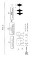
- FIG. 2 describes another example of an ultrawideband communication system that uses a burst oscillation circuit that oscillates only for a certain period of time.
- the reference numeral 201 refers to a baseband circuit
- 202 refers to a burst control signal generation circuit
- 203 refers to a burst oscillation circuit.
- the baseband circuit 201 processes a pre-modified baseband signal generated from data DATA ([1101... ]) and outputs the signal to the burst control signal generation circuit 202 in a UWB communication system that uses a burst oscillation circuit.
- the burst control signal generation circuit 202 generates a burst control signal BCS corresponding to the data ([1101...]) and outputs the burst control signal BCS to the burst oscillation circuit 203.
- the burst oscillation circuit 203 is controlled by the burst control signal BCS so that oscillation occurs when, for example, the BCS (burst control signal) is "H” (oscillation ON), and oscillation is stopped when the BCS is "L” (oscillation OFF).
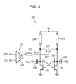
- FIG. 3 is a circuit diagram illustrating an example of a pulse generator that achieves the ultrawideband communication system illustrated in FIG. 2 , and describes the burst control signal generation circuit 202 and the burst oscillation circuit 203.
- the burst control signal generation circuit 202 includes a load 222 and an amplifier 221 that receives the data DATA and a clock CLK, and generates, for example, a burst control signal BCS as described above with reference to FIG. 2 .
- the burst oscillation circuit 203 is configured as a differential amplifier circuit including n-channel type MOS (n-MOS) transistors 231 and 232, a p-channel type MOS (p-MOS) transistor 233, load elements 234 and 235, and capacitors 236 to 239.
- n-MOS n-channel type MOS
- p-MOS p-channel type MOS
- n-MOS transistors 231 and 232 are cross-connected to a gate and a drain through the capacitors 236 and 237, respectively.
- a burst oscillation signal (output signal), Sout is output from the drain of the transistor 231 through the capacitor 238.
- Each of the load elements 234 and 235 may use an inductor or a length of a line, for example.
- the p-MOS transistor 233 is provided between differential terminals of the differential amplifier circuit 203 (between the drains of transistors 231 and 232), and functions as a switch element to control the oscillation corresponding to the burst control signal BCS input to the gate.
- the transistor 233 is turned OFF when the level of the burst control signal BCS is "H” so that the differential amplifier circuit 203 enters an oscillating state.
- the transistor 233 is turned ON when the level is "L” so that the oscillation is stopped.
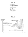
- FIGs. 4A and 4B describe amplitude growth of the pulse generator illustrated in FIG. 3 .
- FIG. 4A illustrates the function of the pulse generator (differential amplifier circuit 203) illustrated in FIG. 3
- FIG. 4B illustrates the output signal (burst oscillation signal) Sout of the differential amplifier circuit 203.
- the differential amplifier circuit (burst oscillation circuit) 203 in FIG. 3 becomes positive feedback circuit of a loop gain G based on the pair of differential transistors 231 and 232 respectively cross-connected to the gate and the drain through the capacitors 236 and 237.
- the burst oscillation signal Sout increases in amplitude due to the loop gain G according to the number of repeats N as illustrated in FIG. 4B .
- the reference numeral T1 in FIG. 4B indicates a timing in which the burst control signal BCS changes from "L” to "H” to enable the oscillation of the burst oscillation circuit 203.
- the reference numeral T2 illustrates a timing in which, for example, a thermal disturbance (random) becomes a trigger to start oscillation
- T3 illustrates a timing in which the oscillated output signal (burst oscillation signal) Sout reaches a desired amplitude.
- the rise time in FIG. 4B indicates a period of time from the timing T2 in which oscillation starts until the timing T3 in which the desired amplitude is achieved.
- the burst oscillation circuit 203 of FIG. 3 does not start oscillating immediately at the timing T1 when the burst control signal BCS changes from “L” to "H”, but starts oscillating from the timing T2 in which the oscillation starts due to a trigger such as the thermal disturbance.
- the pulse generator illustrated in FIG. 3 reaches steady state oscillation at a desired amplitude (T3) after the start of the oscillation (T2) due to noise such as heat and the like and after a certain rise time.
- FIGs. 5A and 5B illustrate a semiconductor integrated circuit of the present embodiment.
- FIG. 5A is a block diagram of the semiconductor integrated circuit of the present embodiment, and
- FIG. 5B illustrates the timing of signals from a pulse generator in the semiconductor integrated circuit of FIG. 5A .
- the semiconductor integrated circuit of the present embodiment includes a baseband circuit 1, a burst control signal generation circuit 2, a burst oscillation circuit 3, and an oscillation start trigger generation circuit 4.
- the baseband circuit 1, the burst control signal generation circuit 2, the burst oscillation circuit 3, and the oscillation start trigger generation circuit 4 may be formed on one semiconductor chip to be configured as the semiconductor integrated circuit.
- the pulse generator of the present embodiment includes the burst control signal generation circuit 2, the burst oscillation circuit 3, and the oscillation start trigger generation circuit 4.
- the baseband circuit 1, the burst control signal generation circuit 2, and the burst oscillation circuit 3 are substantially applicable to the ones described above with reference to FIGs. 2 and 3 .
- the oscillation start trigger generation circuit 4 generates an oscillation start trigger signal OST and outputs the same to the burst oscillation circuit 3.
- the burst oscillation circuit 3 enters a state in which oscillation is possible.
- the oscillation start trigger generation circuit 4 receives the change of the burst control signal BCS from “L” to “H” and outputs the oscillation start trigger signal OST that rises from "L” to "H” to the burst oscillation circuit 3.
- the burst oscillation circuit 3 of the present embodiment forcefully causes the start of oscillation through the oscillation start trigger signal OST in the state in which oscillation is possible when the burst control signal BCS becomes "H" instead of, for example, oscillation being started when a thermal disturbance becomes the trigger.
- the period of time from when the oscillation actually starts until the burst oscillation signal Sout is output may be greatly reduced after the burst oscillation circuit 3 enters the state in which oscillation is possible due to the burst control signal BCS.
- a UWB communication transfer rate may be improved.
- FIG. 6 is a circuit diagram illustrating a portion of a first embodiment of the pulse generator, and illustrates the burst oscillation circuit 3 and the oscillation start trigger generation circuit 4.
- the burst oscillation circuit 3 is configured in a similar way as the burst oscillation circuit 203 described above with reference to FIG. 3 , and includes the n-MOS transistors 31 and 32, the p-MOS transistor 33, the load elements 34 and 35, and the capacitors 36 to 39.
- n-MOS transistors 31 and 32 are respectively cross-connected to a gate and a drain through the capacitors 36 and 37, and the burst oscillation signal (output signal) Sout is output from the drain of the transistor 31 through the capacitor 38.
- the p-MOS transistor 33 is provided between differential terminals of the burst oscillation circuit (differential amplifier circuit) 3, and functions as a switch element to control the oscillation corresponding to the burst control signal BCS input toward the gate.
- the transistor 33 is turned OFF when the level of the burst control signal BCS is high "H” so that the burst oscillation circuit 3 enters an oscillating state (oscillation possible state).
- the transistor 33 is turned ON when the level is low “L” so that the oscillation is stopped.
- the oscillation start trigger generation circuit 4 includes capacitors 41 and 42 and a differential amplifier 43, and outputs differential signals (oscillation start trigger signals) OST and /OST to the gates (differential input terminals) of the pair of differential transistors 31 and 32 through the capacitors 41 and 42.
- the signal /OST indicates a signal with a logic inverse to the signal OST.
- the oscillation start trigger signal OST (and /OST) changes from “L” to "H", for example, immediately after the burst control signal BCS input to the gate of the transistor 33 is changed from “L” to “H” as illustrated in FIG. 5A .
- a desired excitation to oscillation is conducted in the burst oscillation circuit 3 to forcefully start oscillation according to the changes of the oscillation start trigger signals OST and /OST that are input to the control terminals (gates) of the pair of differential transistors 31 and 32.
- the burst oscillation circuit 3 changes the burst control signal BCS to "L" to turn the transistor 33 ON.
- the oscillation is stopped by a short-circuit between the differential terminals of the burst oscillation circuit (differential amplifier circuit) 3.
- the burst oscillation circuit is able to output a burst oscillation signal in a short time period due to an oscillation start trigger signal immediately after entering the state in which oscillation is possible due to a burst control signal.
- the UWB communication transfer rate may be improved.
- FIG. 7 is a circuit diagram illustrating a second embodiment of a pulse generator, and illustrates the burst control signal generation circuit 2, the burst oscillation circuit 3, and the oscillation start trigger generation circuit 4.
- the oscillation start trigger generation circuit 4 in the pulse generator of the second embodiment has capacitors 41 and 42, and four differential amplifiers 431 to 434.
- the burst control signal generation circuit 2 has three differential amplifiers 21 to 23 and a CMOS amplifier 24.
- the first differential amplifier 21 in the burst control signal generation circuit 2 receives, for example, a transfer signal TS from the baseband circuit 1 and outputs a differential output signal to the second differential amplifier 22 and to the oscillation start trigger generation circuit 4.
- the output signal of the first differential amplifier 21 in the burst control signal generation circuit 2 is input into the CMOS amplifier 24 via the second and third differential amplifiers 22 and 23, and a burst control signal BCS is output from the CMOS amplifier 24.
- the burst control signal BCS is input into the gate of the transistor 33 in the burst oscillation circuit 3 so that the oscillation state of the burst oscillation circuit 3 is controlled.
- the burst oscillation circuit 3 of the second embodiment further includes sample-hold circuits 301 and 302 as opposed to the burst oscillation circuit of the first embodiment described above with reference to FIG. 6 .
- Output signals Q are output through the sample-hold circuits 301 and 302.
- the output signal from the first differential amplifier 21 in the burst control signal generation circuit 2 is amplified by the four differential amplifiers 431 to 434 in the oscillation start trigger generation circuit 4 and output as oscillation start trigger signals OST and /OST having sharp rising edges.
- the oscillation start trigger signals OST and /OST are input into the gates of the pair of differential transistors 31 and 32 through the capacitors 41 and 42.
- the reason that the four differential amplifiers are provided in the oscillation start trigger generation circuit 4 is because the timing of differential amplifier 21 output signal to control the switching of the transistor 33 is delayed by the two differential amplifiers 22 and 23 and the CMOS amplifier 24.
- the transistor 33 is controlled by the burst control signal BCS that includes a delay due to the three amplifier circuits 22 to 24, four amplifiers 431 to 434 are provided to generate oscillation start trigger signals OST and /OST that are delayed slightly more than the burst control signal BCS.
- the burst oscillation circuit may output a burst oscillation signal (output signal Q) immediately after entering a state in which oscillation is possible due to the oscillation start trigger signal that is delayed more than the burst control signal.
- the UWB communication transfer rate may be improved.
- FIG. 8 is a circuit diagram illustrating a third embodiment of the pulse generator, and FIG. 9 describes operations of the pulse generator illustrated in FIG. 8.
- FIG. 8 illustrates the burst control signal generation circuit 2, the burst oscillation circuit 3, and the oscillation start trigger generation circuit 4 in the same way as the second embodiment illustrated in FIG. 7 .
- the oscillation start trigger generation circuit 4 in the pulse generator of the third embodiment further includes a T-shaped flip-flop (TFF) 44 in contrast to the pulse generator of the second embodiment illustrated in FIG. 7 .
- TFF T-shaped flip-flop
- the output signal from the first differential amplifier 21 in the burst control signal generation circuit 2 is input into the four differential amplifiers 431 to 434 through the TFF 44 in the oscillation start trigger generation circuit 4.
- the oscillation start trigger generation circuit 4 outputs the oscillation start trigger signal OST with the polarity inverting in order according to the timing in which the output signal (burst control signal BCS) from the differential amplifier 21 changes from “L” to "H” due to the provision of the TFF 44.
- phase of the output signal Q may be alternately inverted due to the inversion of the polarity of the oscillation start trigger signals OST and /OST with each output signal Q (burst oscillation signal Sout).
- the phase of the output signal Q remains the same, the spectral intensity of the oscillation frequency becomes too intense. However, by alternately inverting the phase, the signal intensity of the oscillation frequency may be suppressed.
- the average power may be reduced with the suppression of the oscillation frequency signal intensity by alternately inverting the phase of the output signal Q. Moreover, the effects of noise on other equipment due to the output signal Q may also be reduced.
- the burst oscillation circuit may output the output signal Q immediately after entering a state in which oscillation is possible due to the oscillation start trigger signal that is delayed more than the burst control signal in the same way as in the second embodiment.
- the UWB communication transfer rate may be improved.
- FIGs. 10A and 10B describe the oscillation rise of the pulse generator of the present embodiment.
- FIG. 10A illustrates a rise waveform when an oscillation trigger signal is applied
- FIG. 10B illustrates a rise waveform when no oscillation trigger signal is applied.
- FIG. 10A illustrates a waveform when the output signal (oscillation start trigger signal OST or /OST) of the oscillation start trigger generation circuit 4 is output (ON) in the pulse generator illustrated in FIG. 6 for example
- FIG. 10B illustrates a waveform when the output of the output signal is stopped (OFF).
- An oscillation frequency of 38 GHz is used.
- the period Pa in which the oscillation start trigger signal is ON is slightly shorter than the period Pb.
- the period Pb when the oscillation start trigger signal is OFF as illustrated in FIG. 10B is approximately 550 ns
- the period Pa when the oscillation start trigger signal is ON as illustrated in FIG. 10A is approximately 350 ns.
- the period Pa is approximately 200 ns shorter than the period Pb.
- the effects of reducing the time until the rise of the oscillation changes due to the circuitry and the frequency used and the like.
- the time until the rise of the oscillation may be suitably reduced by applying the oscillation start trigger signal to the burst oscillation circuit to forcefully start the oscillation.
- the effect of reducing the time of the rise of the oscillation is desirable, for example, in a system that uses short pulses as a signal source such as in UWB communication, and may greatly improve the transfer rate.
- the pulse generator of the abovementioned embodiments that includes the burst control signal generation circuit 2, the burst oscillation circuit 3, and the oscillation start trigger generation circuit 4 is not limited to those illustrated in FIGs. 6 to 8 , and may be changed as appropriate.
- the burst oscillation circuit 3 has been described as a differential amplifier circuit in FIGs. 6 to 8 , the burst oscillation circuit 3 is not limited to a differential circuit and may be any circuit that forcefully starts oscillation due to an oscillation start trigger signal instead of a thermal disturbance.
- the pulse generator of the first to third embodiments illustrated in FIGs. 6 to 8 respectively may be a semiconductor integrated circuit formed on one semiconductor chip along with the baseband circuit 1 and the like.
- a pulse generator and a semiconductor integrated circuit have an advantage of a shortened time until it actually starts an oscillation.
- the invention also provides a computer program or a computer program product for carrying out any of the methods described herein, and a computer readable medium having stored thereon a program for carrying out any of the methods described herein.
- a computer program for embodying the invention may be stored on a computer-readable medium, or it could, for example, be in the form of a signal such as a downloadable data signal provided from an Internet website, or it could be in any other form.
Landscapes
- Engineering & Computer Science (AREA)
- Computer Networks & Wireless Communication (AREA)
- Signal Processing (AREA)
- Inductance-Capacitance Distribution Constants And Capacitance-Resistance Oscillators (AREA)
- Stabilization Of Oscillater, Synchronisation, Frequency Synthesizers (AREA)
- Oscillators With Electromechanical Resonators (AREA)
Abstract
Description
- The embodiments discussed herein relate to a pulse generator and a semiconductor integrated circuit.
- Recent developments have focused on ultrawideband (UWB) communication and UWB radar and various techniques have been developed. For example, UWB communication transfer rates have been improved so that as the pulse time width becomes smaller, the bandwidth can be made correspondingly wider.
- Methods using short pulses as a signal source or methods of using a burst oscillation circuit have been adopted to achieve this type of UWB communication and UWB radar. For example, methods using a burst oscillation circuit involve controlling the ON/OFF of the burst oscillation circuit in response to burst control signals to oscillate the burst oscillation circuit for only certain time periods to generate burst oscillation signals.
- Conventionally, various types of pulse generators have been considered for adoption in UWB communication and UWB radar.
- Japanese Laid-open Patent Publication No.
2007-174087 - As described above, a pulse generator adopted for UWB communication and UWB radar is used to control the ON/OFF of a burst oscillation circuit in response to burst control signals.
- Specifically, a transistor switch is provided between differential terminals of a burst oscillation circuit (differential amplification circuit). When the level of a burst control signal is high (H), a switch is turned OFF (oscillating state), and when the level is low (L), the switch is turned ON (oscillation stopped).
- However, a delay is caused in the period of time from switching the transistor from ON to OFF until oscillation actually starts, that is, the time until the oscillation rises in the abovementioned pulse generator.
- This time delay until the rise of oscillation is a serious problem in UWB communication and UWB radar using pulse signals (carriers) in the range of several tens of GHz (e.g., 60 to 90 GHz).
- According to an embodiment of an aspect of the invention, a pulse generator includes an oscillation circuit that generates a burst signal oscillated for ultrawideband band, and a generation circuit that generates a trigger signal that causes oscillation by the oscillation circuit to be started.
- According to an embodiment of another aspect of the invention, a semiconductor circuit comprises a pulse generator including an oscillation circuit that generates a burst oscillation signal for ultrawideband band, and a generation circuit that generates a trigger signal that causes oscillation by the oscillation circuit to be started; and a baseband circuit that processes data and inputs the data into the signal generation circuit.
- Additional aspects and/or advantages will be set forth in part in the description which follows and, in part, will be apparent from the description, or may be learned by practice of the invention.
- These and/or other aspects and advantages will become apparent and more readily appreciated from the following description of the embodiments, taken in conjunction with the accompanying drawings in which:
-
FIG. 1 describes an example of an ultrawideband communication system; -
FIG. 2 describes another example of an ultrawideband communication system; -
FIG. 3 is a circuit diagram illustrating an example of a pulse generator for achieving the ultrawideband communication system illustrated inFIG. 2 ; -
FIGs. 4A and 4B describe amplitude growth in the pulse generator inFIG. 3 ; -
FIGs. 5A and 5B describe a semiconductor integrated circuit of a present embodiment; -
FIG. 6 is a circuit diagram illustrating a portion of a pulse generator of a first embodiment; -
FIG. 7 is a circuit diagram illustrating a pulse generator of a second embodiment; -
FIG. 8 is a circuit diagram illustrating a pulse generator of a third embodiment; -
FIG. 9 describes operations of the pulse generator inFIG. 8 ; and -
FIGs. 10A and 10B describe the oscillation rise generated by the pulse generator of the present embodiment. - Before discussing the embodiments of the pulse generator, an example of an ultrawideband (UWB) communication system, a pulse generator, and problems thereof will be described with reference to
FIGs. 1 to 4B . -
FIG. 1 illustrates an example of an ultrawideband communication system using short pulses as a signal source. InFIG. 1 ,reference numeral 101 refers to a baseband circuit, 102 refers to a pulse generator, and 103 refers to a bandpass filter. - As illustrated in
FIG. 1 , thebaseband circuit 101, for example, processes a pre-modified baseband signal generated from data DATA ([1101...]) and outputs the signal to thepulse generator 102 in a UWB communication system that uses short pulses as a signal source. - The
pulse generator 102, for example, generates short pulses of a time width τ corresponding to the data ([1101...]). After the short pulses are band limited by thebandpass filter 103, a signal (high frequency pulse signal) corresponding to the data ([1101...]) is output. - The pulse generator used in this type of UWB communication system that uses short pulses as a signal source is expensive since a high-
cost bandpass filter 103 is desirably used. -
FIG. 2 describes another example of an ultrawideband communication system that uses a burst oscillation circuit that oscillates only for a certain period of time. InFIG. 2 , thereference numeral 201 refers to a baseband circuit, 202 refers to a burst control signal generation circuit, and 203 refers to a burst oscillation circuit. - As illustrated in
FIG. 2 , thebaseband circuit 201, for example, processes a pre-modified baseband signal generated from data DATA ([1101... ]) and outputs the signal to the burst controlsignal generation circuit 202 in a UWB communication system that uses a burst oscillation circuit. - The burst control
signal generation circuit 202 generates a burst control signal BCS corresponding to the data ([1101...]) and outputs the burst control signal BCS to theburst oscillation circuit 203. - The
burst oscillation circuit 203 is controlled by the burst control signal BCS so that oscillation occurs when, for example, the BCS (burst control signal) is "H" (oscillation ON), and oscillation is stopped when the BCS is "L" (oscillation OFF). -
FIG. 3 is a circuit diagram illustrating an example of a pulse generator that achieves the ultrawideband communication system illustrated inFIG. 2 , and describes the burst controlsignal generation circuit 202 and theburst oscillation circuit 203. - As illustrated in
FIG. 3 , the burst controlsignal generation circuit 202 includes aload 222 and anamplifier 221 that receives the data DATA and a clock CLK, and generates, for example, a burst control signal BCS as described above with reference toFIG. 2 . - The
burst oscillation circuit 203 is configured as a differential amplifier circuit including n-channel type MOS (n-MOS)transistors transistor 233,load elements capacitors 236 to 239. - The n-
MOS transistors capacitors transistor 231 through thecapacitor 238. Each of theload elements - The p-
MOS transistor 233 is provided between differential terminals of the differential amplifier circuit 203 (between the drains oftransistors 231 and 232), and functions as a switch element to control the oscillation corresponding to the burst control signal BCS input to the gate. - Specifically, the
transistor 233 is turned OFF when the level of the burst control signal BCS is "H" so that thedifferential amplifier circuit 203 enters an oscillating state. Thetransistor 233 is turned ON when the level is "L" so that the oscillation is stopped. -
FIGs. 4A and 4B describe amplitude growth of the pulse generator illustrated inFIG. 3 .FIG. 4A illustrates the function of the pulse generator (differential amplifier circuit 203) illustrated inFIG. 3 , andFIG. 4B illustrates the output signal (burst oscillation signal) Sout of thedifferential amplifier circuit 203. - As illustrated in
FIG. 4A , the differential amplifier circuit (burst oscillation circuit) 203 inFIG. 3 becomes positive feedback circuit of a loop gain G based on the pair ofdifferential transistors capacitors - As a result, when the oscillation starts, the burst oscillation signal Sout increases in amplitude due to the loop gain G according to the number of repeats N as illustrated in
FIG. 4B . The reference numeral T1 inFIG. 4B indicates a timing in which the burst control signal BCS changes from "L" to "H" to enable the oscillation of theburst oscillation circuit 203. - The reference numeral T2 illustrates a timing in which, for example, a thermal disturbance (random) becomes a trigger to start oscillation, and T3 illustrates a timing in which the oscillated output signal (burst oscillation signal) Sout reaches a desired amplitude. The rise time in
FIG. 4B indicates a period of time from the timing T2 in which oscillation starts until the timing T3 in which the desired amplitude is achieved. - As illustrated in
FIG. 4B , theburst oscillation circuit 203 ofFIG. 3 does not start oscillating immediately at the timing T1 when the burst control signal BCS changes from "L" to "H", but starts oscillating from the timing T2 in which the oscillation starts due to a trigger such as the thermal disturbance. - Specifically, the pulse generator illustrated in
FIG. 3 reaches steady state oscillation at a desired amplitude (T3) after the start of the oscillation (T2) due to noise such as heat and the like and after a certain rise time. - Although the period of time until steady state oscillation is reached becomes smaller in correspondence to a larger loop gain G of the oscillation circuit (203), improving the loop gain of an oscillation circuit is difficult when the transistor gain is small in ultra-high frequencies such as millimeter wavebands. As a result, it is difficult to reduce the amount of time until the rise of the oscillation.
- Hereinbelow, embodiments of a pulse generator and a semiconductor integrated circuit will be described with reference to the accompanying drawings.
-
FIGs. 5A and 5B illustrate a semiconductor integrated circuit of the present embodiment.FIG. 5A is a block diagram of the semiconductor integrated circuit of the present embodiment, andFIG. 5B illustrates the timing of signals from a pulse generator in the semiconductor integrated circuit ofFIG. 5A . - As illustrated in
FIG. 5A , the semiconductor integrated circuit of the present embodiment includes abaseband circuit 1, a burst controlsignal generation circuit 2, aburst oscillation circuit 3, and an oscillation starttrigger generation circuit 4. - The
baseband circuit 1, the burst controlsignal generation circuit 2, theburst oscillation circuit 3, and the oscillation starttrigger generation circuit 4 may be formed on one semiconductor chip to be configured as the semiconductor integrated circuit. As described hereinbelow, the pulse generator of the present embodiment includes the burst controlsignal generation circuit 2, theburst oscillation circuit 3, and the oscillation starttrigger generation circuit 4. - The
baseband circuit 1, the burst controlsignal generation circuit 2, and theburst oscillation circuit 3 are substantially applicable to the ones described above with reference toFIGs. 2 and3 . The oscillation starttrigger generation circuit 4 generates an oscillation start trigger signal OST and outputs the same to theburst oscillation circuit 3. - As illustrated in
FIG. 5B , when the burst control signal BCS changes from a low level "L" to a high level "H", theburst oscillation circuit 3 enters a state in which oscillation is possible. The oscillation starttrigger generation circuit 4 receives the change of the burst control signal BCS from "L" to "H" and outputs the oscillation start trigger signal OST that rises from "L" to "H" to theburst oscillation circuit 3. - Specifically, the
burst oscillation circuit 3 of the present embodiment forcefully causes the start of oscillation through the oscillation start trigger signal OST in the state in which oscillation is possible when the burst control signal BCS becomes "H" instead of, for example, oscillation being started when a thermal disturbance becomes the trigger. - As a result, the period of time from when the oscillation actually starts until the burst oscillation signal Sout is output may be greatly reduced after the
burst oscillation circuit 3 enters the state in which oscillation is possible due to the burst control signal BCS. As a result, for example, a UWB communication transfer rate may be improved. -
FIG. 6 is a circuit diagram illustrating a portion of a first embodiment of the pulse generator, and illustrates theburst oscillation circuit 3 and the oscillation starttrigger generation circuit 4. - As illustrated in
FIG. 6 , theburst oscillation circuit 3 is configured in a similar way as theburst oscillation circuit 203 described above with reference toFIG. 3 , and includes the n-MOS transistors MOS transistor 33, theload elements capacitors 36 to 39. - The n-
MOS transistors capacitors transistor 31 through thecapacitor 38. - The p-
MOS transistor 33 is provided between differential terminals of the burst oscillation circuit (differential amplifier circuit) 3, and functions as a switch element to control the oscillation corresponding to the burst control signal BCS input toward the gate. - Specifically, the
transistor 33 is turned OFF when the level of the burst control signal BCS is high "H" so that theburst oscillation circuit 3 enters an oscillating state (oscillation possible state). Thetransistor 33 is turned ON when the level is low "L" so that the oscillation is stopped. - The oscillation start
trigger generation circuit 4 includescapacitors differential amplifier 43, and outputs differential signals (oscillation start trigger signals) OST and /OST to the gates (differential input terminals) of the pair ofdifferential transistors capacitors - The oscillation start trigger signal OST (and /OST) changes from "L" to "H", for example, immediately after the burst control signal BCS input to the gate of the
transistor 33 is changed from "L" to "H" as illustrated inFIG. 5A . - A desired excitation to oscillation is conducted in the
burst oscillation circuit 3 to forcefully start oscillation according to the changes of the oscillation start trigger signals OST and /OST that are input to the control terminals (gates) of the pair ofdifferential transistors - The reason that the
capacitors differential amplifier 43 and the gates of the pair ofdifferential transistors burst oscillation circuit 3 to start. - The
burst oscillation circuit 3 changes the burst control signal BCS to "L" to turn thetransistor 33 ON. The oscillation is stopped by a short-circuit between the differential terminals of the burst oscillation circuit (differential amplifier circuit) 3. - In this way, according to the pulse generator of the first embodiment, the burst oscillation circuit is able to output a burst oscillation signal in a short time period due to an oscillation start trigger signal immediately after entering the state in which oscillation is possible due to a burst control signal. As a result, for example, the UWB communication transfer rate may be improved.
-
FIG. 7 is a circuit diagram illustrating a second embodiment of a pulse generator, and illustrates the burst controlsignal generation circuit 2, theburst oscillation circuit 3, and the oscillation starttrigger generation circuit 4. - As may be seen when comparing
FIG. 7 withFIG. 6 described above, the oscillation starttrigger generation circuit 4 in the pulse generator of the second embodiment hascapacitors differential amplifiers 431 to 434. - The burst control
signal generation circuit 2 has threedifferential amplifiers 21 to 23 and aCMOS amplifier 24. The firstdifferential amplifier 21 in the burst controlsignal generation circuit 2 receives, for example, a transfer signal TS from thebaseband circuit 1 and outputs a differential output signal to the seconddifferential amplifier 22 and to the oscillation starttrigger generation circuit 4. - The output signal of the first
differential amplifier 21 in the burst controlsignal generation circuit 2 is input into theCMOS amplifier 24 via the second and thirddifferential amplifiers CMOS amplifier 24. The burst control signal BCS is input into the gate of thetransistor 33 in theburst oscillation circuit 3 so that the oscillation state of theburst oscillation circuit 3 is controlled. - The
burst oscillation circuit 3 of the second embodiment further includes sample-hold circuits FIG. 6 . Output signals Q are output through the sample-hold circuits - The output signal from the first
differential amplifier 21 in the burst controlsignal generation circuit 2 is amplified by the fourdifferential amplifiers 431 to 434 in the oscillation starttrigger generation circuit 4 and output as oscillation start trigger signals OST and /OST having sharp rising edges. The oscillation start trigger signals OST and /OST are input into the gates of the pair ofdifferential transistors capacitors - The reason that the four differential amplifiers are provided in the oscillation start
trigger generation circuit 4 is because the timing ofdifferential amplifier 21 output signal to control the switching of thetransistor 33 is delayed by the twodifferential amplifiers CMOS amplifier 24. - That is, since the
transistor 33 is controlled by the burst control signal BCS that includes a delay due to the threeamplifier circuits 22 to 24, fouramplifiers 431 to 434 are provided to generate oscillation start trigger signals OST and /OST that are delayed slightly more than the burst control signal BCS. - In this way, according to the pulse generator of the embodiment, the burst oscillation circuit may output a burst oscillation signal (output signal Q) immediately after entering a state in which oscillation is possible due to the oscillation start trigger signal that is delayed more than the burst control signal. As a result, for example, the UWB communication transfer rate may be improved.
-
FIG. 8 is a circuit diagram illustrating a third embodiment of the pulse generator, andFIG. 9 describes operations of the pulse generator illustrated inFIG. 8. FIG. 8 illustrates the burst controlsignal generation circuit 2, theburst oscillation circuit 3, and the oscillation starttrigger generation circuit 4 in the same way as the second embodiment illustrated inFIG. 7 . - As may be seen by comparing
FIG. 8 with the abovementionedFIG. 7 , the oscillation starttrigger generation circuit 4 in the pulse generator of the third embodiment further includes a T-shaped flip-flop (TFF) 44 in contrast to the pulse generator of the second embodiment illustrated inFIG. 7 . - The output signal from the first
differential amplifier 21 in the burst controlsignal generation circuit 2 is input into the fourdifferential amplifiers 431 to 434 through theTFF 44 in the oscillation starttrigger generation circuit 4. - As illustrated in
FIG. 9 , the oscillation starttrigger generation circuit 4 outputs the oscillation start trigger signal OST with the polarity inverting in order according to the timing in which the output signal (burst control signal BCS) from thedifferential amplifier 21 changes from "L" to "H" due to the provision of theTFF 44. - That is, the phase of the output signal Q may be alternately inverted due to the inversion of the polarity of the oscillation start trigger signals OST and /OST with each output signal Q (burst oscillation signal Sout).
- If the phase of the output signal Q remains the same, the spectral intensity of the oscillation frequency becomes too intense. However, by alternately inverting the phase, the signal intensity of the oscillation frequency may be suppressed.
- In this way, according to the pulse generator of the third embodiment, the average power may be reduced with the suppression of the oscillation frequency signal intensity by alternately inverting the phase of the output signal Q. Moreover, the effects of noise on other equipment due to the output signal Q may also be reduced.
- In this way, according to the pulse generator of the third embodiment, the burst oscillation circuit may output the output signal Q immediately after entering a state in which oscillation is possible due to the oscillation start trigger signal that is delayed more than the burst control signal in the same way as in the second embodiment. As a result, for example, the UWB communication transfer rate may be improved.
-
FIGs. 10A and 10B describe the oscillation rise of the pulse generator of the present embodiment.FIG. 10A illustrates a rise waveform when an oscillation trigger signal is applied, andFIG. 10B illustrates a rise waveform when no oscillation trigger signal is applied. - That is,
FIG. 10A illustrates a waveform when the output signal (oscillation start trigger signal OST or /OST) of the oscillation starttrigger generation circuit 4 is output (ON) in the pulse generator illustrated inFIG. 6 for example, andFIG. 10B illustrates a waveform when the output of the output signal is stopped (OFF). An oscillation frequency of 38 GHz is used. - As may be seen when comparing the
FIGs. 10A and 10B , among the periods Pa and Pb from the rise of the burst control signal BCS to "H" until the output signal Q reaches the desired amplitude, the period Pa in which the oscillation start trigger signal is ON is slightly shorter than the period Pb. - That is, whereas the period Pb when the oscillation start trigger signal is OFF as illustrated in
FIG. 10B is approximately 550 ns, the period Pa when the oscillation start trigger signal is ON as illustrated inFIG. 10A is approximately 350 ns. Thus, it may be seen that the period Pa is approximately 200 ns shorter than the period Pb. - The effects of reducing the time until the rise of the oscillation changes due to the circuitry and the frequency used and the like. However, the time until the rise of the oscillation may be suitably reduced by applying the oscillation start trigger signal to the burst oscillation circuit to forcefully start the oscillation.
- The effect of reducing the time of the rise of the oscillation is desirable, for example, in a system that uses short pulses as a signal source such as in UWB communication, and may greatly improve the transfer rate.
- As described hereinbelow, the pulse generator of the abovementioned embodiments that includes the burst control
signal generation circuit 2, theburst oscillation circuit 3, and the oscillation starttrigger generation circuit 4 is not limited to those illustrated inFIGs. 6 to 8 , and may be changed as appropriate. - For example, although the
burst oscillation circuit 3 has been described as a differential amplifier circuit inFIGs. 6 to 8 , theburst oscillation circuit 3 is not limited to a differential circuit and may be any circuit that forcefully starts oscillation due to an oscillation start trigger signal instead of a thermal disturbance. - Furthermore, as illustrated in
FIG. 5A , the pulse generator of the first to third embodiments illustrated inFIGs. 6 to 8 respectively may be a semiconductor integrated circuit formed on one semiconductor chip along with thebaseband circuit 1 and the like. - According to the embodiments, a pulse generator and a semiconductor integrated circuit have an advantage of a shortened time until it actually starts an oscillation.
- In any of the above aspects, the various features may be implemented in hardware, or as software modules running on one or more processors. Features of on aspect may be applied to any of the other aspects.
- The invention also provides a computer program or a computer program product for carrying out any of the methods described herein, and a computer readable medium having stored thereon a program for carrying out any of the methods described herein. A computer program for embodying the invention may be stored on a computer-readable medium, or it could, for example, be in the form of a signal such as a downloadable data signal provided from an Internet website, or it could be in any other form.
- All examples and conditional language recited herein are intended for pedagogical purposes to aid the reader in understanding the invention and the concepts contributed by the inventor to furthering the art, and are to be construed as being without limitation to such specifically recited examples and conditions, nor does the organization of such examples in the specification relate to a showing of the superiority and inferiority of the invention. Although the embodiments of the present invention have been described in detail, it should be understood that the various changes, substitutions, and alterations could be made hereto without departing from the spirit and scope of the invention.
Claims (11)
- A pulse generator, comprising:an oscillation circuit that generates a burst signal oscillated for ultrawideband band; anda generation circuit that generates a trigger signal that causes oscillation by the oscillation circuit to be started.
- The pulse generator according to claim 1, further comprising:a signal generation circuit that generates a control signal to control an oscillation state of the oscillation circuit.
- The pulse generator according to claim 2, wherein
the generation circuit generates the trigger signal according to the control signal. - The pulse generator according to claim 2 or claim 3, wherein
the oscillation circuit is a differential amplifier circuit including
a first differential transistor and a second differential transistor that are cross-connected to conduct oscillation, and
a switch element that controls the oscillation state of the oscillation circuit based on the control signal. - The pulse generator according to claim 4, wherein
the switch element is provided between differential terminals of the differential amplifier circuit; and
the differential amplifier circuit enters a state in which oscillation is possible when the switch element is turned off by the control signal. - The pulse generator according to claim 4 or claim 5, wherein
the trigger signal is input into the control terminals of the first and second transistors. - The pulse generator according to any one of claims 2 to 6, wherein
the oscillation circuit enters a state in which oscillation is stopped when the control signal is a first level, and enters a state in which oscillation is possible when the control signal is a second level that is different from the first level. - The pulse generator according to claim 7, wherein
the generation circuit generates the trigger signal with a polarity that inverts in order according to a timing in which the control signal changes from the first level to the second level. - The pulse generator according to claim 8, wherein
the trigger signal includes:a first polarity signal that is input as a positive signal into the control terminal of the first transistor, and is input as a negative signal into the control terminal of the second transistor; anda second polarity signal that is input as a negative signal into the control terminal of the first transistor, and is input as a positive signal into the control terminal of the second transistor; and whereinthe generation circuit alternately generates the first polarity signal and the second polarity signal and outputs the oscillation signal in which the phase is alternately inverted. - A semiconductor circuit, comprising:a pulse generator including
an oscillation circuit that generates a burst oscillation signal for ultrawideband band, and
a generation circuit that generates a trigger signal that causes oscillation by the oscillation circuit to be started; anda baseband circuit that processes data and inputs the data into the signal generation circuit. - The semiconductor circuit according to claim 10, wherein
the pulse generator and the baseband circuit are formed on the same semiconductor chip.
Applications Claiming Priority (1)
| Application Number | Priority Date | Filing Date | Title |
|---|---|---|---|
| JP2011288280A JP5831222B2 (en) | 2011-12-28 | 2011-12-28 | Pulse generator and semiconductor integrated circuit |
Publications (3)
| Publication Number | Publication Date |
|---|---|
| EP2611032A2 true EP2611032A2 (en) | 2013-07-03 |
| EP2611032A3 EP2611032A3 (en) | 2015-12-30 |
| EP2611032B1 EP2611032B1 (en) | 2023-06-07 |
Family
ID=47143568
Family Applications (1)
| Application Number | Title | Priority Date | Filing Date |
|---|---|---|---|
| EP12189870.4A Active EP2611032B1 (en) | 2011-12-28 | 2012-10-25 | Pulse generator and semiconductor integrated circuit |
Country Status (3)
| Country | Link |
|---|---|
| US (1) | US8860520B2 (en) |
| EP (1) | EP2611032B1 (en) |
| JP (1) | JP5831222B2 (en) |
Families Citing this family (1)
| Publication number | Priority date | Publication date | Assignee | Title |
|---|---|---|---|---|
| US8981861B2 (en) * | 2012-06-08 | 2015-03-17 | Hittite Microwave Corporation | Injection locked pulsed oscillator |
Citations (1)
| Publication number | Priority date | Publication date | Assignee | Title |
|---|---|---|---|---|
| JP2007174087A (en) | 2005-12-20 | 2007-07-05 | Matsushita Electric Ind Co Ltd | Pulse generation circuit |
Family Cites Families (15)
| Publication number | Priority date | Publication date | Assignee | Title |
|---|---|---|---|---|
| JPS5015532B1 (en) * | 1970-08-29 | 1975-06-05 | ||
| DE69809748T2 (en) * | 1997-07-18 | 2003-09-11 | Kohler Co., Kohler | RADAR DEVICE FOR LOW POWER USE AND SANITARY SYSTEMS |
| US6781470B2 (en) * | 2001-09-26 | 2004-08-24 | General Atomics | Tunable oscillator |
| CN1906499B (en) * | 2004-10-14 | 2010-06-02 | 安立股份有限公司 | Small-sized, low-power short-range radar and control method for arbitrarily changing delay time between transmission and reception with high time resolution |
| CN1918793B (en) * | 2004-11-15 | 2011-11-16 | 安立股份有限公司 | High-frequency electronic switch, bust wave generation device using the same, and short pulse radar using the same |
| US7474164B2 (en) * | 2005-01-28 | 2009-01-06 | Anritas Corporation | Radar oscillator |
| EP1843170A1 (en) * | 2005-01-28 | 2007-10-10 | Anritsu Corporation | Uwb short pulse radar |
| WO2007139131A1 (en) * | 2006-06-01 | 2007-12-06 | The Furukawa Electric Co., Ltd. | Burst oscillation device, burst oscillation method, and distance measurement communication system |
| JP4685060B2 (en) * | 2006-06-08 | 2011-05-18 | パナソニック株式会社 | Differential oscillator |
| JP4982260B2 (en) * | 2006-06-20 | 2012-07-25 | パナソニック株式会社 | Pulse modulation circuit |
| US7719373B2 (en) * | 2006-10-27 | 2010-05-18 | Imec | Device and method for generating a signal with predefined transcient at start-up |
| WO2008069444A1 (en) * | 2006-12-06 | 2008-06-12 | Electronics And Telecommunications Research Institute | Ultra-low power pulse generator for multiband impulse radio-ultra wideband system and method using the same |
| US8160118B2 (en) * | 2008-12-19 | 2012-04-17 | Lawrence Livermore National Security, Llc | UWB dual burst transmit driver |
| US8427242B2 (en) * | 2009-01-15 | 2013-04-23 | Zebra Enterprises Solutions Corp. | Ultra wideband on-chip pulse generator |
| JP2010171970A (en) * | 2009-01-21 | 2010-08-05 | Korea Advanced Inst Of Science & Technology | Multi-phase ultra-wideband signal generator using differential pulse oscillators and array thereof |
-
2011
- 2011-12-28 JP JP2011288280A patent/JP5831222B2/en not_active Expired - Fee Related
-
2012
- 2012-10-23 US US13/658,108 patent/US8860520B2/en active Active
- 2012-10-25 EP EP12189870.4A patent/EP2611032B1/en active Active
Patent Citations (1)
| Publication number | Priority date | Publication date | Assignee | Title |
|---|---|---|---|---|
| JP2007174087A (en) | 2005-12-20 | 2007-07-05 | Matsushita Electric Ind Co Ltd | Pulse generation circuit |
Non-Patent Citations (1)
| Title |
|---|
| TUAN-ANH PHAN ET AL.: "A 18-pJ/Pulse OOK CMOS Transmitter for Multiband UWB Impulse Radio", IEEE MICROWAVE AND WIRELESS COMPONENTS LETTERS, vol. 17, no. 9, September 2007 (2007-09-01) |
Also Published As
| Publication number | Publication date |
|---|---|
| EP2611032B1 (en) | 2023-06-07 |
| JP2013138337A (en) | 2013-07-11 |
| US20130169372A1 (en) | 2013-07-04 |
| US8860520B2 (en) | 2014-10-14 |
| JP5831222B2 (en) | 2015-12-09 |
| EP2611032A3 (en) | 2015-12-30 |
Similar Documents
| Publication | Publication Date | Title |
|---|---|---|
| US8487670B2 (en) | Divide-by-two injection-locked ring oscillator circuit | |
| TWI628912B (en) | Reduce the duration of the start-up period of the crystal oscillator circuit | |
| US20170040941A1 (en) | Injection-locked oscillator and method for controlling jitter and/or phase noise | |
| US8570076B2 (en) | Parallel path frequency divider circuit | |
| CN106487334B (en) | Capacitor arrangement for an oscillator | |
| US20110043291A1 (en) | Dynamic limiters for frequency dividers | |
| EP3226410A1 (en) | Crystal oscillator circuit | |
| US20090115540A1 (en) | Controllable oscillating system and related method for selectively adjusting currents passing through cross-coupling driving device | |
| JP2010028809A (en) | Method and apparatus for achieving 50% duty cycle on output vco of phase locked loop | |
| WO2016108989A1 (en) | Cross-coupled level shifter with transition tracking circuits | |
| JP2008042890A (en) | Pulse modulation circuit and pulse modulation method | |
| US8860520B2 (en) | Pulse generator and semiconductor integrated circuit | |
| US9369085B1 (en) | Oscillator with favorable startup | |
| EP1536561A1 (en) | Current controlled oscillator | |
| US8552785B2 (en) | Pulse generator | |
| US11095426B1 (en) | Method and apparatus for clock recovery | |
| US20090219064A1 (en) | Pulse generator circuit and communication apparatus | |
| US10637451B2 (en) | Pulse position modulation circuit and transmission circuit | |
| US9595980B2 (en) | Oscillation circuit and transmitter including the same | |
| CN116131769A (en) | Low noise amplifier | |
| US8217727B1 (en) | Slew rate edge enhancer | |
| US20130099841A1 (en) | Noise reduction device and semiconductor device having the same | |
| JP7084232B2 (en) | Signal transduction device | |
| JP5832398B2 (en) | Signal transmission circuit | |
| Yousef et al. | Multi-phase ring oscillator with minimized phase noise for ultra-wideband applications |
Legal Events
| Date | Code | Title | Description |
|---|---|---|---|
| PUAI | Public reference made under article 153(3) epc to a published international application that has entered the european phase |
Free format text: ORIGINAL CODE: 0009012 |
|
| AK | Designated contracting states |
Kind code of ref document: A2 Designated state(s): AL AT BE BG CH CY CZ DE DK EE ES FI FR GB GR HR HU IE IS IT LI LT LU LV MC MK MT NL NO PL PT RO RS SE SI SK SM TR |
|
| AX | Request for extension of the european patent |
Extension state: BA ME |
|
| PUAL | Search report despatched |
Free format text: ORIGINAL CODE: 0009013 |
|
| AK | Designated contracting states |
Kind code of ref document: A3 Designated state(s): AL AT BE BG CH CY CZ DE DK EE ES FI FR GB GR HR HU IE IS IT LI LT LU LV MC MK MT NL NO PL PT RO RS SE SI SK SM TR |
|
| AX | Request for extension of the european patent |
Extension state: BA ME |
|
| RIC1 | Information provided on ipc code assigned before grant |
Ipc: H04B 1/717 20110101ALI20151120BHEP Ipc: H03K 3/354 20060101AFI20151120BHEP |
|
| 17P | Request for examination filed |
Effective date: 20160204 |
|
| RBV | Designated contracting states (corrected) |
Designated state(s): AL AT BE BG CH CY CZ DE DK EE ES FI FR GB GR HR HU IE IS IT LI LT LU LV MC MK MT NL NO PL PT RO RS SE SI SK SM TR |
|
| STAA | Information on the status of an ep patent application or granted ep patent |
Free format text: STATUS: EXAMINATION IS IN PROGRESS |
|
| 17Q | First examination report despatched |
Effective date: 20190228 |
|
| GRAP | Despatch of communication of intention to grant a patent |
Free format text: ORIGINAL CODE: EPIDOSNIGR1 |
|
| STAA | Information on the status of an ep patent application or granted ep patent |
Free format text: STATUS: GRANT OF PATENT IS INTENDED |
|
| INTG | Intention to grant announced |
Effective date: 20230324 |
|
| GRAS | Grant fee paid |
Free format text: ORIGINAL CODE: EPIDOSNIGR3 |
|
| GRAA | (expected) grant |
Free format text: ORIGINAL CODE: 0009210 |
|
| STAA | Information on the status of an ep patent application or granted ep patent |
Free format text: STATUS: THE PATENT HAS BEEN GRANTED |
|
| AK | Designated contracting states |
Kind code of ref document: B1 Designated state(s): AL AT BE BG CH CY CZ DE DK EE ES FI FR GB GR HR HU IE IS IT LI LT LU LV MC MK MT NL NO PL PT RO RS SE SI SK SM TR |
|
| REG | Reference to a national code |
Ref country code: GB Ref legal event code: FG4D |
|
| REG | Reference to a national code |
Ref country code: CH Ref legal event code: EP Ref country code: AT Ref legal event code: REF Ref document number: 1577883 Country of ref document: AT Kind code of ref document: T Effective date: 20230615 |
|
| REG | Reference to a national code |
Ref country code: DE Ref legal event code: R096 Ref document number: 602012079631 Country of ref document: DE |
|
| REG | Reference to a national code |
Ref country code: LT Ref legal event code: MG9D |
|
| REG | Reference to a national code |
Ref country code: NL Ref legal event code: MP Effective date: 20230607 |
|
| PG25 | Lapsed in a contracting state [announced via postgrant information from national office to epo] |
Ref country code: SE Free format text: LAPSE BECAUSE OF FAILURE TO SUBMIT A TRANSLATION OF THE DESCRIPTION OR TO PAY THE FEE WITHIN THE PRESCRIBED TIME-LIMIT Effective date: 20230607 Ref country code: NO Free format text: LAPSE BECAUSE OF FAILURE TO SUBMIT A TRANSLATION OF THE DESCRIPTION OR TO PAY THE FEE WITHIN THE PRESCRIBED TIME-LIMIT Effective date: 20230907 Ref country code: ES Free format text: LAPSE BECAUSE OF FAILURE TO SUBMIT A TRANSLATION OF THE DESCRIPTION OR TO PAY THE FEE WITHIN THE PRESCRIBED TIME-LIMIT Effective date: 20230607 |
|
| PGFP | Annual fee paid to national office [announced via postgrant information from national office to epo] |
Ref country code: GB Payment date: 20230801 Year of fee payment: 12 |
|
| REG | Reference to a national code |
Ref country code: AT Ref legal event code: MK05 Ref document number: 1577883 Country of ref document: AT Kind code of ref document: T Effective date: 20230607 |
|
| PG25 | Lapsed in a contracting state [announced via postgrant information from national office to epo] |
Ref country code: RS Free format text: LAPSE BECAUSE OF FAILURE TO SUBMIT A TRANSLATION OF THE DESCRIPTION OR TO PAY THE FEE WITHIN THE PRESCRIBED TIME-LIMIT Effective date: 20230607 Ref country code: NL Free format text: LAPSE BECAUSE OF FAILURE TO SUBMIT A TRANSLATION OF THE DESCRIPTION OR TO PAY THE FEE WITHIN THE PRESCRIBED TIME-LIMIT Effective date: 20230607 Ref country code: LV Free format text: LAPSE BECAUSE OF FAILURE TO SUBMIT A TRANSLATION OF THE DESCRIPTION OR TO PAY THE FEE WITHIN THE PRESCRIBED TIME-LIMIT Effective date: 20230607 Ref country code: LT Free format text: LAPSE BECAUSE OF FAILURE TO SUBMIT A TRANSLATION OF THE DESCRIPTION OR TO PAY THE FEE WITHIN THE PRESCRIBED TIME-LIMIT Effective date: 20230607 Ref country code: HR Free format text: LAPSE BECAUSE OF FAILURE TO SUBMIT A TRANSLATION OF THE DESCRIPTION OR TO PAY THE FEE WITHIN THE PRESCRIBED TIME-LIMIT Effective date: 20230607 Ref country code: GR Free format text: LAPSE BECAUSE OF FAILURE TO SUBMIT A TRANSLATION OF THE DESCRIPTION OR TO PAY THE FEE WITHIN THE PRESCRIBED TIME-LIMIT Effective date: 20230908 |
|
| PGFP | Annual fee paid to national office [announced via postgrant information from national office to epo] |
Ref country code: FR Payment date: 20230801 Year of fee payment: 12 |
|
| PG25 | Lapsed in a contracting state [announced via postgrant information from national office to epo] |
Ref country code: FI Free format text: LAPSE BECAUSE OF FAILURE TO SUBMIT A TRANSLATION OF THE DESCRIPTION OR TO PAY THE FEE WITHIN THE PRESCRIBED TIME-LIMIT Effective date: 20230607 |
|
| PG25 | Lapsed in a contracting state [announced via postgrant information from national office to epo] |
Ref country code: SK Free format text: LAPSE BECAUSE OF FAILURE TO SUBMIT A TRANSLATION OF THE DESCRIPTION OR TO PAY THE FEE WITHIN THE PRESCRIBED TIME-LIMIT Effective date: 20230607 |
|
| PG25 | Lapsed in a contracting state [announced via postgrant information from national office to epo] |
Ref country code: IS Free format text: LAPSE BECAUSE OF FAILURE TO SUBMIT A TRANSLATION OF THE DESCRIPTION OR TO PAY THE FEE WITHIN THE PRESCRIBED TIME-LIMIT Effective date: 20231007 |
|
| PG25 | Lapsed in a contracting state [announced via postgrant information from national office to epo] |
Ref country code: SM Free format text: LAPSE BECAUSE OF FAILURE TO SUBMIT A TRANSLATION OF THE DESCRIPTION OR TO PAY THE FEE WITHIN THE PRESCRIBED TIME-LIMIT Effective date: 20230607 Ref country code: SK Free format text: LAPSE BECAUSE OF FAILURE TO SUBMIT A TRANSLATION OF THE DESCRIPTION OR TO PAY THE FEE WITHIN THE PRESCRIBED TIME-LIMIT Effective date: 20230607 Ref country code: RO Free format text: LAPSE BECAUSE OF FAILURE TO SUBMIT A TRANSLATION OF THE DESCRIPTION OR TO PAY THE FEE WITHIN THE PRESCRIBED TIME-LIMIT Effective date: 20230607 Ref country code: PT Free format text: LAPSE BECAUSE OF FAILURE TO SUBMIT A TRANSLATION OF THE DESCRIPTION OR TO PAY THE FEE WITHIN THE PRESCRIBED TIME-LIMIT Effective date: 20231009 Ref country code: IS Free format text: LAPSE BECAUSE OF FAILURE TO SUBMIT A TRANSLATION OF THE DESCRIPTION OR TO PAY THE FEE WITHIN THE PRESCRIBED TIME-LIMIT Effective date: 20231007 Ref country code: EE Free format text: LAPSE BECAUSE OF FAILURE TO SUBMIT A TRANSLATION OF THE DESCRIPTION OR TO PAY THE FEE WITHIN THE PRESCRIBED TIME-LIMIT Effective date: 20230607 Ref country code: CZ Free format text: LAPSE BECAUSE OF FAILURE TO SUBMIT A TRANSLATION OF THE DESCRIPTION OR TO PAY THE FEE WITHIN THE PRESCRIBED TIME-LIMIT Effective date: 20230607 Ref country code: AT Free format text: LAPSE BECAUSE OF FAILURE TO SUBMIT A TRANSLATION OF THE DESCRIPTION OR TO PAY THE FEE WITHIN THE PRESCRIBED TIME-LIMIT Effective date: 20230607 |
|
| PGFP | Annual fee paid to national office [announced via postgrant information from national office to epo] |
Ref country code: DE Payment date: 20230801 Year of fee payment: 12 |
|
| PG25 | Lapsed in a contracting state [announced via postgrant information from national office to epo] |
Ref country code: PL Free format text: LAPSE BECAUSE OF FAILURE TO SUBMIT A TRANSLATION OF THE DESCRIPTION OR TO PAY THE FEE WITHIN THE PRESCRIBED TIME-LIMIT Effective date: 20230607 |
|
| REG | Reference to a national code |
Ref country code: DE Ref legal event code: R097 Ref document number: 602012079631 Country of ref document: DE |
|
| PLBE | No opposition filed within time limit |
Free format text: ORIGINAL CODE: 0009261 |
|
| STAA | Information on the status of an ep patent application or granted ep patent |
Free format text: STATUS: NO OPPOSITION FILED WITHIN TIME LIMIT |
|
| PG25 | Lapsed in a contracting state [announced via postgrant information from national office to epo] |
Ref country code: DK Free format text: LAPSE BECAUSE OF FAILURE TO SUBMIT A TRANSLATION OF THE DESCRIPTION OR TO PAY THE FEE WITHIN THE PRESCRIBED TIME-LIMIT Effective date: 20230607 |
|
| PG25 | Lapsed in a contracting state [announced via postgrant information from national office to epo] |
Ref country code: SI Free format text: LAPSE BECAUSE OF FAILURE TO SUBMIT A TRANSLATION OF THE DESCRIPTION OR TO PAY THE FEE WITHIN THE PRESCRIBED TIME-LIMIT Effective date: 20230607 |
|
| 26N | No opposition filed |
Effective date: 20240308 |
|
| PG25 | Lapsed in a contracting state [announced via postgrant information from national office to epo] |
Ref country code: SI Free format text: LAPSE BECAUSE OF FAILURE TO SUBMIT A TRANSLATION OF THE DESCRIPTION OR TO PAY THE FEE WITHIN THE PRESCRIBED TIME-LIMIT Effective date: 20230607 Ref country code: IT Free format text: LAPSE BECAUSE OF FAILURE TO SUBMIT A TRANSLATION OF THE DESCRIPTION OR TO PAY THE FEE WITHIN THE PRESCRIBED TIME-LIMIT Effective date: 20230607 Ref country code: MC Free format text: LAPSE BECAUSE OF FAILURE TO SUBMIT A TRANSLATION OF THE DESCRIPTION OR TO PAY THE FEE WITHIN THE PRESCRIBED TIME-LIMIT Effective date: 20230607 |
|
| REG | Reference to a national code |
Ref country code: CH Ref legal event code: PL |
|
| REG | Reference to a national code |
Ref country code: BE Ref legal event code: MM Effective date: 20231031 |
|
| PG25 | Lapsed in a contracting state [announced via postgrant information from national office to epo] |
Ref country code: LU Free format text: LAPSE BECAUSE OF NON-PAYMENT OF DUE FEES Effective date: 20231025 |
|
| PG25 | Lapsed in a contracting state [announced via postgrant information from national office to epo] |
Ref country code: LU Free format text: LAPSE BECAUSE OF NON-PAYMENT OF DUE FEES Effective date: 20231025 |
|
| PG25 | Lapsed in a contracting state [announced via postgrant information from national office to epo] |
Ref country code: CH Free format text: LAPSE BECAUSE OF NON-PAYMENT OF DUE FEES Effective date: 20231031 |
|
| PG25 | Lapsed in a contracting state [announced via postgrant information from national office to epo] |
Ref country code: CH Free format text: LAPSE BECAUSE OF NON-PAYMENT OF DUE FEES Effective date: 20231031 |
|
| PG25 | Lapsed in a contracting state [announced via postgrant information from national office to epo] |
Ref country code: BE Free format text: LAPSE BECAUSE OF NON-PAYMENT OF DUE FEES Effective date: 20231031 |
|
| PG25 | Lapsed in a contracting state [announced via postgrant information from national office to epo] |
Ref country code: IE Free format text: LAPSE BECAUSE OF NON-PAYMENT OF DUE FEES Effective date: 20231025 |
|
| PG25 | Lapsed in a contracting state [announced via postgrant information from national office to epo] |
Ref country code: IE Free format text: LAPSE BECAUSE OF NON-PAYMENT OF DUE FEES Effective date: 20231025 |
|
| PG25 | Lapsed in a contracting state [announced via postgrant information from national office to epo] |
Ref country code: BG Free format text: LAPSE BECAUSE OF FAILURE TO SUBMIT A TRANSLATION OF THE DESCRIPTION OR TO PAY THE FEE WITHIN THE PRESCRIBED TIME-LIMIT Effective date: 20230607 |
|
| PG25 | Lapsed in a contracting state [announced via postgrant information from national office to epo] |
Ref country code: BG Free format text: LAPSE BECAUSE OF FAILURE TO SUBMIT A TRANSLATION OF THE DESCRIPTION OR TO PAY THE FEE WITHIN THE PRESCRIBED TIME-LIMIT Effective date: 20230607 |
|
| REG | Reference to a national code |
Ref country code: DE Ref legal event code: R119 Ref document number: 602012079631 Country of ref document: DE |
|
| GBPC | Gb: european patent ceased through non-payment of renewal fee |
Effective date: 20241025 |
|
| PG25 | Lapsed in a contracting state [announced via postgrant information from national office to epo] |
Ref country code: DE Free format text: LAPSE BECAUSE OF NON-PAYMENT OF DUE FEES Effective date: 20250501 |
|
| PG25 | Lapsed in a contracting state [announced via postgrant information from national office to epo] |
Ref country code: GB Free format text: LAPSE BECAUSE OF NON-PAYMENT OF DUE FEES Effective date: 20241025 |
|
| PG25 | Lapsed in a contracting state [announced via postgrant information from national office to epo] |
Ref country code: FR Free format text: LAPSE BECAUSE OF NON-PAYMENT OF DUE FEES Effective date: 20241031 |
|
| PG25 | Lapsed in a contracting state [announced via postgrant information from national office to epo] |
Ref country code: CY Free format text: LAPSE BECAUSE OF FAILURE TO SUBMIT A TRANSLATION OF THE DESCRIPTION OR TO PAY THE FEE WITHIN THE PRESCRIBED TIME-LIMIT; INVALID AB INITIO Effective date: 20121025 |
|
| PG25 | Lapsed in a contracting state [announced via postgrant information from national office to epo] |
Ref country code: HU Free format text: LAPSE BECAUSE OF FAILURE TO SUBMIT A TRANSLATION OF THE DESCRIPTION OR TO PAY THE FEE WITHIN THE PRESCRIBED TIME-LIMIT; INVALID AB INITIO Effective date: 20121025 |
|
| PG25 | Lapsed in a contracting state [announced via postgrant information from national office to epo] |
Ref country code: TR Free format text: LAPSE BECAUSE OF FAILURE TO SUBMIT A TRANSLATION OF THE DESCRIPTION OR TO PAY THE FEE WITHIN THE PRESCRIBED TIME-LIMIT Effective date: 20230607 |