EP2611015B1 - Zero-voltage-switching (ZVS) piezoelectric driving circuit - Google Patents
Zero-voltage-switching (ZVS) piezoelectric driving circuit Download PDFInfo
- Publication number
- EP2611015B1 EP2611015B1 EP20120199270 EP12199270A EP2611015B1 EP 2611015 B1 EP2611015 B1 EP 2611015B1 EP 20120199270 EP20120199270 EP 20120199270 EP 12199270 A EP12199270 A EP 12199270A EP 2611015 B1 EP2611015 B1 EP 2611015B1
- Authority
- EP
- European Patent Office
- Prior art keywords
- voltage
- side switch
- switch set
- shunt
- zero
- Prior art date
- Legal status (The legal status is an assumption and is not a legal conclusion. Google has not performed a legal analysis and makes no representation as to the accuracy of the status listed.)
- Active
Links
Images



Classifications
-
- H—ELECTRICITY
- H02—GENERATION; CONVERSION OR DISTRIBUTION OF ELECTRIC POWER
- H02M—APPARATUS FOR CONVERSION BETWEEN AC AND AC, BETWEEN AC AND DC, OR BETWEEN DC AND DC, AND FOR USE WITH MAINS OR SIMILAR POWER SUPPLY SYSTEMS; CONVERSION OF DC OR AC INPUT POWER INTO SURGE OUTPUT POWER; CONTROL OR REGULATION THEREOF
- H02M7/00—Conversion of AC power input into DC power output; Conversion of DC power input into AC power output
- H02M7/42—Conversion of DC power input into AC power output without possibility of reversal
- H02M7/44—Conversion of DC power input into AC power output without possibility of reversal by static converters
- H02M7/48—Conversion of DC power input into AC power output without possibility of reversal by static converters using discharge tubes with control electrode or semiconductor devices with control electrode
-
- H—ELECTRICITY
- H02—GENERATION; CONVERSION OR DISTRIBUTION OF ELECTRIC POWER
- H02P—CONTROL OR REGULATION OF ELECTRIC MOTORS, ELECTRIC GENERATORS OR DYNAMO-ELECTRIC CONVERTERS; CONTROLLING TRANSFORMERS, REACTORS OR CHOKE COILS
- H02P31/00—Arrangements for regulating or controlling electric motors not provided for in groups H02P1/00 - H02P5/00, H02P7/00 or H02P21/00 - H02P29/00
-
- H—ELECTRICITY
- H02—GENERATION; CONVERSION OR DISTRIBUTION OF ELECTRIC POWER
- H02M—APPARATUS FOR CONVERSION BETWEEN AC AND AC, BETWEEN AC AND DC, OR BETWEEN DC AND DC, AND FOR USE WITH MAINS OR SIMILAR POWER SUPPLY SYSTEMS; CONVERSION OF DC OR AC INPUT POWER INTO SURGE OUTPUT POWER; CONTROL OR REGULATION THEREOF
- H02M5/00—Conversion of AC power input into AC power output, e.g. for change of voltage, for change of frequency, for change of number of phases
- H02M5/02—Conversion of AC power input into AC power output, e.g. for change of voltage, for change of frequency, for change of number of phases without intermediate conversion into DC
- H02M5/04—Conversion of AC power input into AC power output, e.g. for change of voltage, for change of frequency, for change of number of phases without intermediate conversion into DC by static converters
- H02M5/22—Conversion of AC power input into AC power output, e.g. for change of voltage, for change of frequency, for change of number of phases without intermediate conversion into DC by static converters using discharge tubes with control electrode or semiconductor devices with control electrode
- H02M5/275—Conversion of AC power input into AC power output, e.g. for change of voltage, for change of frequency, for change of number of phases without intermediate conversion into DC by static converters using discharge tubes with control electrode or semiconductor devices with control electrode using devices of a triode or transistor type requiring continuous application of a control signal
- H02M5/293—Conversion of AC power input into AC power output, e.g. for change of voltage, for change of frequency, for change of number of phases without intermediate conversion into DC by static converters using discharge tubes with control electrode or semiconductor devices with control electrode using devices of a triode or transistor type requiring continuous application of a control signal using semiconductor devices only
-
- H—ELECTRICITY
- H05—ELECTRIC TECHNIQUES NOT OTHERWISE PROVIDED FOR
- H05B—ELECTRIC HEATING; ELECTRIC LIGHT SOURCES NOT OTHERWISE PROVIDED FOR; CIRCUIT ARRANGEMENTS FOR ELECTRIC LIGHT SOURCES, IN GENERAL
- H05B41/00—Circuit arrangements or apparatus for igniting or operating discharge lamps
- H05B41/14—Circuit arrangements
- H05B41/26—Circuit arrangements in which the lamp is fed by power derived from DC by means of a converter, e.g. by high-voltage DC
- H05B41/28—Circuit arrangements in which the lamp is fed by power derived from DC by means of a converter, e.g. by high-voltage DC using static converters
- H05B41/282—Circuit arrangements in which the lamp is fed by power derived from DC by means of a converter, e.g. by high-voltage DC using static converters with semiconductor devices
- H05B41/2825—Circuit arrangements in which the lamp is fed by power derived from DC by means of a converter, e.g. by high-voltage DC using static converters with semiconductor devices by means of a bridge converter in the final stage
- H05B41/2827—Circuit arrangements in which the lamp is fed by power derived from DC by means of a converter, e.g. by high-voltage DC using static converters with semiconductor devices by means of a bridge converter in the final stage using specially adapted components in the load circuit, e.g. feed-back transformers, piezoelectric transformers; using specially adapted load circuit configurations
-
- H—ELECTRICITY
- H10—SEMICONDUCTOR DEVICES; ELECTRIC SOLID-STATE DEVICES NOT OTHERWISE PROVIDED FOR
- H10N—ELECTRIC SOLID-STATE DEVICES NOT OTHERWISE PROVIDED FOR
- H10N30/00—Piezoelectric or electrostrictive devices
- H10N30/40—Piezoelectric or electrostrictive devices with electrical input and electrical output, e.g. functioning as transformers
-
- H—ELECTRICITY
- H10—SEMICONDUCTOR DEVICES; ELECTRIC SOLID-STATE DEVICES NOT OTHERWISE PROVIDED FOR
- H10N—ELECTRIC SOLID-STATE DEVICES NOT OTHERWISE PROVIDED FOR
- H10N30/00—Piezoelectric or electrostrictive devices
- H10N30/80—Constructional details
- H10N30/802—Circuitry or processes for operating piezoelectric or electrostrictive devices not otherwise provided for, e.g. drive circuits
- H10N30/804—Circuitry or processes for operating piezoelectric or electrostrictive devices not otherwise provided for, e.g. drive circuits for piezoelectric transformers
-
- H—ELECTRICITY
- H02—GENERATION; CONVERSION OR DISTRIBUTION OF ELECTRIC POWER
- H02M—APPARATUS FOR CONVERSION BETWEEN AC AND AC, BETWEEN AC AND DC, OR BETWEEN DC AND DC, AND FOR USE WITH MAINS OR SIMILAR POWER SUPPLY SYSTEMS; CONVERSION OF DC OR AC INPUT POWER INTO SURGE OUTPUT POWER; CONTROL OR REGULATION THEREOF
- H02M1/00—Details of apparatus for conversion
- H02M1/0048—Circuits or arrangements for reducing losses
- H02M1/0054—Transistor switching losses
- H02M1/0058—Transistor switching losses by employing soft switching techniques, i.e. commutation of transistors when applied voltage is zero or when current flow is zero
-
- H—ELECTRICITY
- H02—GENERATION; CONVERSION OR DISTRIBUTION OF ELECTRIC POWER
- H02M—APPARATUS FOR CONVERSION BETWEEN AC AND AC, BETWEEN AC AND DC, OR BETWEEN DC AND DC, AND FOR USE WITH MAINS OR SIMILAR POWER SUPPLY SYSTEMS; CONVERSION OF DC OR AC INPUT POWER INTO SURGE OUTPUT POWER; CONTROL OR REGULATION THEREOF
- H02M7/00—Conversion of AC power input into DC power output; Conversion of DC power input into AC power output
- H02M7/42—Conversion of DC power input into AC power output without possibility of reversal
- H02M7/44—Conversion of DC power input into AC power output without possibility of reversal by static converters
- H02M7/48—Conversion of DC power input into AC power output without possibility of reversal by static converters using discharge tubes with control electrode or semiconductor devices with control electrode
- H02M7/4815—Resonant converters
-
- Y—GENERAL TAGGING OF NEW TECHNOLOGICAL DEVELOPMENTS; GENERAL TAGGING OF CROSS-SECTIONAL TECHNOLOGIES SPANNING OVER SEVERAL SECTIONS OF THE IPC; TECHNICAL SUBJECTS COVERED BY FORMER USPC CROSS-REFERENCE ART COLLECTIONS [XRACs] AND DIGESTS
- Y02—TECHNOLOGIES OR APPLICATIONS FOR MITIGATION OR ADAPTATION AGAINST CLIMATE CHANGE
- Y02B—CLIMATE CHANGE MITIGATION TECHNOLOGIES RELATED TO BUILDINGS, e.g. HOUSING, HOUSE APPLIANCES OR RELATED END-USER APPLICATIONS
- Y02B70/00—Technologies for an efficient end-user side electric power management and consumption
- Y02B70/10—Technologies improving the efficiency by using switched-mode power supplies [SMPS], i.e. efficient power electronics conversion e.g. power factor correction or reduction of losses in power supplies or efficient standby modes
Definitions
- the present invention relates to a zero-voltage-switching (ZVS) piezoelectric driving circuit, and in particular to a piezoelectric driving circuit of a Zero-Voltage-Switching (ZVS) half-bridge circuit, capable of operating in a wide bandwidth and in a wide range of load.
- ZVS zero-voltage-switching
- the piezoelectric transformer Due to its advantages of compact size, thin profile, and free of Electromagnetic Interference (EMI), the piezoelectric transformer has been used extensively in the power driving circuits. However, the piezoelectric transformer still has insurmountable problems.
- an inductor In applying a piezoelectric transformer into a bridge switching circuit, usually, an inductor has to be connected between the bridge switching circuit and the piezoelectric transformer, to achieve Zero-voltage-Switching.
- the inductor itself is thicker than the piezoelectric transformer (namely, having a larger dimension), such that it has to sacrifice the advantages of thin profile of the piezoelectric transformer.
- the disposition of inductor in the main circuit could cause additional power loss and electromagnetic interference (EMI).
- JP 2000-312474 A relates to a power supply equipment having a half bridge circuit, a piezoelectric transformer and a shunt circuit.
- the shunt circuit includes a capacitor and an inductor, thus foaming a passive linear circuit, so that input current of the piezoelectric transformer is varied according to the difference of the load and the operation frequency. Therefore, presently, the design and performance of the piezoelectric transformer is not quite satisfactory, and it has much room for improvements.
- the present invention provides a zero-voltage-switching (ZVS) piezoelectric driving circuit, to overcome the deficiency and drawback of the prior art.
- ZVS zero-voltage-switching
- a major objective of the present invention is to provide a zero-voltage-switching (ZVS) piezoelectric driving circuit, to utilize a shunt circuit to assist resonance in the dead time of a half-bridge switch, so as to achieve ZVS for a varying load and a varying operation frequency.
- ZVS zero-voltage-switching
- Another objective of the present invention is to provide a zero-voltage-switching (ZVS) piezoelectric driving circuit.
- ZVS zero-voltage-switching
- a shunt circuit replaces an ordinary inductor in the main current route, to reduce the space occupied and power loss, and to achieve a thin profile and raised effectiveness of the entire circuit, hereby enhancing the development and application of this technology, and competitiveness of the product.
- the present invention provides a zero-voltage-switching (ZVS) piezoelectric driving circuit, comprising: a half-bridge driving circuit, a piezoelectric element, and a first and a second shunt circuit.
- the half-bridge driving circuit is used to receive an input DC voltage, and it includes a high-side switch set and a low-side switch set connected in series, to convert the input DC voltage into AC voltage through switching the high-side switch set and a low-side switch set.
- the piezoelectric element is connected electrically to the half-bridge driving circuit, to receive the AC voltage and drive a load.
- the first and the second shunt circuit are connected electrically between the half-bridge driving circuit and the piezoelectric element.
- the first and the second shunt circuit resonate with the half-bridge driving circuit, so that the high-side switch set and the low-side switch set perform zero-voltage-switching (ZVS).
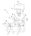
- Fig. 1 is a circuit diagram of a zero-voltage-switching (ZVS) piezoelectric driving circuit according to a first example, which is not in accordance with the present invention, but helpful for the understanding thereof.
- the zero-voltage-switching (ZVS) piezoelectric driving circuit 10 includes: a half-bridge driving circuit 12, a piezoelectric element 14, and at least a shunt circuit 16.
- the half-bridge driving circuit 12 includes a high-side switch set 18 and a low-side switch set 20 connected in series.
- the half-bridge driving circuit 12 receives an input DC voltage (V DC ), and converts it into an AC voltage of square wave through switching the high-side switch set 18 and the low-side switch set 20.
- V DC input DC voltage
- the piezoelectric element 14 is connected electrically to the half-bridge driving circuit 12, to receive the AC voltage to perform resonance, and then drive a load 22 into actions.
- the load 22 can be a Cold Cathode Fluorescent Lamp (CCFL), a Hot Cathode Fluorescent Lamp (HCFL), a High Intensity Discharge (HID) Lamp, a Light-Emitting-Diode (LED), a rectifier circuit, a piezoelectric actuator, and a switching circuit.
- the shunt circuit 16 is connected electrically between the half-bridge driving circuit 12 and the piezoelectric element 14. The shunt circuit 16 resonates with the half-bridge driving circuit 12, such that the high-side switch set 18 and a low-side switch set 20 perform zero-voltage-switching (ZVS), and that will described in detail later.
- the high-side switch set 18 includes a first parasitic capacitance (C K1 ) 182 and a first parasitic diode 184.
- the low-side switch set 20 includes a second parasitic capacitance (C K2 ) 202 and a second parasitic diode 204.
- the piezoelectric element 14 can be a piezoelectric transformer or a piezoelectric resonator. Herein, the piezoelectric transformer is taken as an example for explanation, and it includes an input capacitor (C P ) 142.
- a set of shunt circuits 16 are taken as example for explanation, and it includes a shunt inductor (L S ) 162, a dual-direction switch (K S ) 164, and a shunt power supply (V DC /2) 166.
- the shunt power supply 166 provides a driving voltage to the dual-direction switch (K S ) 164, such that the DC voltage of the shunt power supply 166 is half the input DC voltage (V DC ).
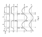
- Fig. 2 a waveform diagram of an AC voltage on a zero-voltage-switching (ZVS) piezoelectric driving circuit according to the first prior art example.
- ZVS zero-voltage-switching
- the high-side switch set 18 and the low-side switch set 20 are both switched off, and this period is the dead time of the conventional half-bridge circuit.
- the shunt circuit 16 is turned on, such that the input capacitor 142, the second parasitic capacitance 202, the first parasitic capacitance 182, and the shunt inductor 162 start to resonate, so that the input capacitor 142 and the second parasitic capacitance 202 start to resonate and discharge through the shunt circuit 16. Meanwhile, the first parasitic capacitance 182 starts to resonate and is charged.
- V P across the input capacitor 142 decrements to zero voltage by a positive and sinusoidal slope, while the voltage across the high-side switch set 18 increments to the level of the input DC voltage (V DC ), such that it could serve as the critical condition for the zero-voltage-switching (ZVS) of the low-side switch set 20.
- V DC input DC voltage
- ZVS zero-voltage-switching
- the parasitic inductance produced on the conduction wire of the shunt circuit 16, or the minute inductance produced by the wire on the printed-circuit-board (PCB) of the shunt circuit 16 can be used to match the input capacitor 142, the first parasitic capacitance 182, and the second parasitic capacitance 202 to perform resonance.
- the voltage V P across the input capacitor 142 is discharged to zero, that operation period is over.
- the high-side switch set 18, the low-side switch set 20, and the shunt circuits 16 are switched off at the same time.
- the second parasitic diode 204 of the low-side switch set 20 is turned on, to provide current i m to flow through the piezoelectric element 14.
- the high-side switch set 18 is switched off, while the low-side switch set 20 is switched on.
- the shunt circuit 16 is still turned off.
- the high-side switch set 18 is switched from switching off to switching on, the input voltage of the piezoelectric element 14 is zero, namely, the voltage V P across the input capacitor 142 is zero, and it will remain at zero after it is switched, thus achieving zero-voltage-switching (ZVS).
- ZVS zero-voltage-switching
- the high-side switch set 18 and the low-side switch set 20 are both switched off.
- the shunt circuit 16 starts to be turned on, the same as that in the operation period [t 1 -t 2 ].
- the input capacitor 142, the second parasitic capacitance 202, the first parasitic capacitance 182, and the shunt inductor 162 starts to resonate, so that the input capacitor 142, the second parasitic capacitance 202 start to resonate and discharge through the shunt circuit 16, meanwhile the first parasitic capacitance 182 starts to resonate and is charged.
- the voltage V P across the input capacitor 142 increments to the level of input DC voltage (V DC ) by a positive and sinusoidal slope, while the voltage across the high-side switch set 18 decrements to zero voltage by a positive and sinusoidal slope, such that it could serve as the critical condition for the zero-voltage-switching (ZVS) of high-side switch set 18.
- ZVS zero-voltage-switching
- the input capacitor 142 is not able to discharge completely to zero, such that the high-side switch set 18 is not able to perform zero-voltage-switching-on in the next operation period.
- the voltage V P across the input capacitor 142 is charged to the level of the input DC voltage (V DC ), that operation period is over.
- the high-side switch set 18, the low-side switch set 20, and the shunt circuits 16 are switched off at the same time.
- the voltage V P across the input capacitor 142 starts to be charged to the level of input DC voltage (V DC ).
- the first parasitic diode 184 of the high-side switch set 18 is turned on, to provide current i m to flow through the piezoelectric element 14.
- the high-side switch set 18 and the low-side switch set 20 are switched on respectively in operation period [t 0 -t 1 ] and operation period [t 3 -t 4 ]. In other operation period, the high-side switch set 18 and the low-side switch set 20 are both switched off, and this is the dead times of half-bridge driving circuit 12.
- the input capacitor 142, the second parasitic capacitance 202, the first parasitic capacitance 182, and the shunt inductor 162 start to resonate to charge, or it is discharged through the shunt circuit 16, to achieve zero-voltage-switching (ZVS).
- ZVS zero-voltage-switching
- shunt circuit 16 is configured to enable the half-bridge driving circuit 12 to achieve zero-voltage-switching (ZVS), but it has first to satisfy the following two conditions, as shown in equations (3) to (6):
- K S is dual-direction switch 164
- T S is the switching-on period of the dual-direction switch 164, such as the operation period [t 1 -t 2 ] or [t 4 -t 5 ]
- i S is the current of shunt circuit 16.
- the two conditions of zero-voltage-switching are: a sufficiently long dead time and a sufficiently large current i s of the shunt circuit 16, and they are not related to other factors (such as frequency and load).
- the current is of the shunt circuit 16 is determined based on the input DC voltage (V DC ), shunt inductor 162 (L S ) and input capacitor 142 (C P ), the first parasitic capacitance 182 (C K1 ), the second parasitic capacitance 202 (C K2 ), and they are all the conventional elements.
- the dead time when the dead time is fixed, then the conditions for zero-voltage-saitching (ZVS) are fixed, and they are not related to operation frequency and load, to achieve wide bandwidth of zero-voltage-switching (ZVS).
- the corresponding frequency for period t d is 1/t d , such that the upper limit of operation frequency of the shunt circuit 16 is 1/t d .
- Fig. 3 a circuit diagram of a zero-voltage-switching (ZVS) piezoelectric driving circuit according to the present invention.
- the second embodiment is in fact a design of a dual-direction switch incorporating a half-bridge driving circuit, namely, the shunt circuit is designed into two groups.
- two shunt circuits are connected electrically between the half-bridge driving circuit 12 and the piezoelectric element 14, namely, a first shunt circuit 24 and a second shunt circuit 26.
- the first shunt circuit 24 includes a first shunt inductor 242 (L 1 ) and a first single-direction switch 244 (S 1 ) connected in series.
- the second shunt circuit 26 is connected to the first shunt circuit 24.
- the second shunt circuit 26 includes a second shunt inductor 262 (L 2 ) and a second single-direction switch 264 (S 2 ) connected in series.
- the compositions of the half-bridge driving circuit 12 and the piezoelectric element 14 are the same as the first embodiment, and they will not be repeated here for brevity.
- the first shunt circuit 24 is connected directly to the input DC voltage (V DC ), to be used as driving voltage V 1
- the second shunt circuit 26 is connected directly to ground (0V), to be used as driving voltage V 2 .
- outside power supply can be omitted, to simplify the overall circuit design.
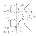
- Fig. 4 a waveform diagram of an AC voltage on a zero-voltage-switching (ZVS) piezoelectric driving circuit according to the present invention.
- ZVS zero-voltage-switching
- V DC input DC voltage
- ZVS zero-voltage-switching
- the resonance period [t 1 -t 2 ] of the second shunt inductor 262 and the total capacitance can be obtained through the following equation 7: t 5 - t 4 > ⁇ ⁇ L s ⁇ C p + C K ⁇ 1 + C K ⁇ 2
- the operation period [t 1 -t 2 ] is rather short, so during resonance, a small inductor can be used directly on the first shunt circuit 24 and the second shunt circuit 26 to match the total capacitance on the piezoelectric driving circuit 10.
- a small inductor can be used directly on the first shunt circuit 24 and the second shunt circuit 26 to match the total capacitance on the piezoelectric driving circuit 10.
- the high-side switch set 18, the low-side switch set 20, and the first shunt circuit 24 are switched off at the same time.
- the second single-direction switch 264 of the second shunt circuit 26 is still switched on, but the voltage V P across input capacitor 142 becomes zero.
- the second parasitic diode 204 of the low-side switch set 20 is switched on, to provide current i m to flow through the piezoelectric element 14. Meanwhile, the remaining current (i S2 ) on the second shunt inductor 262 is discharged linearly.
- the second shunt circuit 26 When the charges on the second shunt inductor 262 are discharged completely, the second shunt circuit 26 is turned off automatically. Then, the second single-direction switch 264 can be switched off in the present operation period or the next operation period under the condition of zero-voltage-switching (ZVS), since no current flows through the second shunt circuit 26. In fact, in the next operation period, the second single-direction switch 264 is switched off at a slower switching speed. When the low-side switch set 20 starts to be switched on, that operation period is over.
- ZVS zero-voltage-switching
- the high-side switch set 18 and the low-side switch set 20 are both switched on.
- the first shunt circuit 24 and the second shunt circuit 26 are both turned off. Therefore, the input voltage of the piezoelectric element 14 is zero, namely, voltage V P across the input capacitor 142 is zero.
- the low-side switch set 20 is switched to a switch-off, that operation period is over.
- the high-side switch set 18 and the low-side switch set 20 are both switched off.
- the input capacitor 142, the second parasitic capacitance 202, the first parasitic capacitance 182, and the second shunt inductor 264 start to resonate, so that the input capacitor 142 and the second parasitic capacitance 202 start to resonate and charge through the first shunt circuit 24. Meanwhile, the first parasitic capacitance 182 starts to resonate and discharge.
- the voltage V P across the input capacitor 142 increments to the level of the input DC voltage (V DC ) by a positive and sinusoidal slope
- the voltage across the high-side switch set 18 decrements to zero voltage by a positive and sinusoidal slope , such that it could serve as the critical condition for the zero-voltage-switching (ZVS) of the high-side switch set 18.
- ZVS zero-voltage-switching
- the resonance discharge current is not sufficiently large, then the input capacitor 142 is not able to discharge completely to zero, such that the high-side switch set 18 is not able to perform zero-voltage-switching-on in the next operation period.
- the voltage V P across the input capacitor 142 is charged to the level of the input DC voltage (V DC ), that operation period is over.
- the high-side switch set 18 and the low-side switch set 20 are switched on respectively in operation periods [t 0 -t 1 ] and [t 3 -t 4 ]. In other operation periods, the high-side switch set 18 and the low-side switch set 20 are switched off, and this is the dead time of half-bridge driving circuit 12.
- the input capacitor 142, the second parasitic capacitance 202, the first parasitic capacitance 182, and the first shunt inductor 242, and the second shunt inductor 262 start to resonate to charge, or they are discharged through the first shunt inductor 242 and the second shunt inductor 262, to achieve zero-voltage-switching (ZVS).
- ZVS zero-voltage-switching
- ZVS zero-voltage-switching
- Fig. 5 a circuit diagram of a zero-voltage-switching (ZVS) piezoelectric driving circuit according to another example, which is not in accordance with the present invention but helpful for the understanding thereof.
- the difference between the third embodiment and the first embodiment is that, in the third embodiment, a first capacitor (C 1 ) 28, a second capacitor (C 2 ) 30, and a shunt capacitor (C S ) 32 are added.
- the high-side switch set 18 is connected to the first capacitor 28 in parallel
- the piezoelectric element 14 is connected to the second capacitor 30 in parallel.
- the shunt capacitor 32 is connected in series between the first capacitor 28 and the shunt circuit 16.
- the second capacitor 30 is capable of changing the value of shunt current is in the shunt circuit 16, and the resonance frequency (f S ) of the first capacitor 28 and the shunt circuit 16.
- the first capacitor 28 and the second capacitor 30 can be used to reduce the resonance frequency (f S ), and increase the current is in the shunt circuit 16.
- the shunt capacitor 32 can be used to increase the resonance frequency (f S ), and reduce the current is in the shunt circuit 16.
- the addition of the capacitors mentioned above is capable of making design of the zero-voltage-switching (ZVS) of the piezoelectric driving circuit 10 more flexible.
- Fig. 6 a circuit diagram of a zero-voltage-switching (ZVS) piezoelectric driving circuit according to a further example, which is not in accordance with the present invention, but helpful for the understanding thereof.
- the piezoelectric element is a piezoelectric resonator 34, such that a third capacitor (C P2 ) 36 replaces the second capacitor (C 2 ), and the mechanical resonance L m -C m -R m of the original piezoelectric transformer is replaced by the mechanical resonance L m2 -C m2 -R m2 of the piezoelectric resonator 34.
- the piezoelectric resonator 34 replaces the piezoelectric transformer to transfer energy, thus eliminating the output capacitor (C out ) of the original piezoelectric transformer.
- the current i m will flow into the output capacitor (C out ) and the load 22, while in the example of piezoelectric resonator 34, current i m will flow directly into the load 22. Since current i m (vibration speed) is the physical restriction of piezoelectric resonator, in the condition of the same current i m , piezoelectric resonator 34 is able to obtain more watts of output power for the load 22, thus simplifying even more the entire circuit design.
- Zero-Voltage-Switching can not be maintained for frequency variation feedback control and large range load variations, and frequency range applicable is too narrow, as such limiting the development and application of that technology.
- the present invention proposes to use shunt circuits to replace bulky inductor, and also utilizes the shunt circuits to assist resonance in the dead time of the half-bridge switch, so that Zero-Voltage-Switching (ZVS) can be maintained for varying load and varying operation frequency.
- shunt circuits replace the ordinary inductor in the main current route to save the space occupied and reduce the energy loss. As such, the entire circuit can be of a thinner profile, while its effectiveness is raised, that is beneficial to the development and application of the technology, and the competitiveness of the product.
Landscapes
- Engineering & Computer Science (AREA)
- Power Engineering (AREA)
- Inverter Devices (AREA)
- Circuit Arrangements For Discharge Lamps (AREA)
- Dc-Dc Converters (AREA)
Description
- The present invention relates to a zero-voltage-switching (ZVS) piezoelectric driving circuit, and in particular to a piezoelectric driving circuit of a Zero-Voltage-Switching (ZVS) half-bridge circuit, capable of operating in a wide bandwidth and in a wide range of load.
- Due to its advantages of compact size, thin profile, and free of Electromagnetic Interference (EMI), the piezoelectric transformer has been used extensively in the power driving circuits. However, the piezoelectric transformer still has insurmountable problems. By way of example, in applying a piezoelectric transformer into a bridge switching circuit, usually, an inductor has to be connected between the bridge switching circuit and the piezoelectric transformer, to achieve Zero-voltage-Switching. However, the inductor itself is thicker than the piezoelectric transformer (namely, having a larger dimension), such that it has to sacrifice the advantages of thin profile of the piezoelectric transformer. In addition, the disposition of inductor in the main circuit could cause additional power loss and electromagnetic interference (EMI).
- Moreover, by not including an inductor in a piezoelectric transformer driving circuit, though it can achieve Zero-Voltage-Switching (ZVS) for a specific load range, yet the frequency range applicable is just too narrow, so that the piezoelectric transformer is not able to keep up ZVS operations under the conditions of frequency variation feedback control and large range load variations. In fact, without regard to whether piezoelectric transformer is used in cooperation with an inductor, the frequency range for the driving circuit to achieve ZVS is rather narrow. Furthermore, in actual application, piezoelectric transformer is difficult to achieve ZVS for a light load, when it is far away from resonance frequency. For this reason, the development and application of piezoelectric transformer in power supply is rather limited.
-
JP 2000-312474 A
Therefore, presently, the design and performance of the piezoelectric transformer is not quite satisfactory, and it has much room for improvements. - In view of the problems and shortcomings of the prior art, the present invention provides a zero-voltage-switching (ZVS) piezoelectric driving circuit, to overcome the deficiency and drawback of the prior art.
- A major objective of the present invention is to provide a zero-voltage-switching (ZVS) piezoelectric driving circuit, to utilize a shunt circuit to assist resonance in the dead time of a half-bridge switch, so as to achieve ZVS for a varying load and a varying operation frequency.
- Another objective of the present invention is to provide a zero-voltage-switching (ZVS) piezoelectric driving circuit. Wherein, a shunt circuit replaces an ordinary inductor in the main current route, to reduce the space occupied and power loss, and to achieve a thin profile and raised effectiveness of the entire circuit, hereby enhancing the development and application of this technology, and competitiveness of the product.
- The above mentioned objects are solved by the zero-voltage-switching (ZVS) piezoelectric driving circuit according to
claim 1. Advantageous improvements of the invention are described by dependent claims. In order to achieve the above objective, the present invention provides a zero-voltage-switching (ZVS) piezoelectric driving circuit, comprising: a half-bridge driving circuit, a piezoelectric element, and a first and a second shunt circuit. The half-bridge driving circuit is used to receive an input DC voltage, and it includes a high-side switch set and a low-side switch set connected in series, to convert the input DC voltage into AC voltage through switching the high-side switch set and a low-side switch set. The piezoelectric element is connected electrically to the half-bridge driving circuit, to receive the AC voltage and drive a load. The first and the second shunt circuit are connected electrically between the half-bridge driving circuit and the piezoelectric element. The first and the second shunt circuit resonate with the half-bridge driving circuit, so that the high-side switch set and the low-side switch set perform zero-voltage-switching (ZVS). - Further scope of the applicability of the present invention will become apparent from the detailed descriptions given hereinafter. However, it should be understood that the detailed descriptions and specific examples, while indicating preferred embodiments of the present invention, are given by way of illustration only, since various changes and modifications within the scope of the present invention will become apparent to those skilled in the art from this detailed descriptions.
- The related drawings in connection with the detailed descriptions of the present invention to be made later are described briefly as follows, in which:
-
Fig. 1 is a circuit diagram of a zero-voltage-switching (ZVS) piezoelectric driving circuit according to a first prior art example; -
Fig. 2 is a waveform diagram of an AC voltage on a zero-voltage-switching (ZVS) piezoelectric driving circuit according to the first prior art example; -
Fig. 3 is a circuit diagram of a zero-voltage-switching (ZVS) piezoelectric driving circuit according to the present invention; -
Fig. 4 is a waveform diagram of an AC voltage on a zero-voltage-switching (ZVS) piezoelectric driving circuit according to the present invention; -
Fig. 5 is a circuit diagram of a zero-voltage-switching (ZVS) piezoelectric driving circuit according to another prior art example; and -
Fig. 6 is a circuit diagram of a zero-voltage-switching (ZVS) piezoelectric driving circuit according to a further prior art example. - The purpose, construction, features, functions and advantages of the present invention can be appreciated and understood more thoroughly through the following detailed description with reference to the attached drawings.
-
Fig. 1 is a circuit diagram of a zero-voltage-switching (ZVS) piezoelectric driving circuit according to a first example, which is not in accordance with the present invention, but helpful for the understanding thereof. As shown inFig. 1 , the zero-voltage-switching (ZVS)piezoelectric driving circuit 10 includes: a half-bridge driving circuit 12, apiezoelectric element 14, and at least ashunt circuit 16. The half-bridge driving circuit 12 includes a high-side switch set 18 and a low-side switch set 20 connected in series. The half-bridge driving circuit 12 receives an input DC voltage (VDC), and converts it into an AC voltage of square wave through switching the high-side switch set 18 and the low-side switch set 20. Thepiezoelectric element 14 is connected electrically to the half-bridge driving circuit 12, to receive the AC voltage to perform resonance, and then drive aload 22 into actions. Wherein, theload 22 can be a Cold Cathode Fluorescent Lamp (CCFL), a Hot Cathode Fluorescent Lamp (HCFL), a High Intensity Discharge (HID) Lamp, a Light-Emitting-Diode (LED), a rectifier circuit, a piezoelectric actuator, and a switching circuit. Theshunt circuit 16 is connected electrically between the half-bridge driving circuit 12 and thepiezoelectric element 14. Theshunt circuit 16 resonates with the half-bridge driving circuit 12, such that the high-side switch set 18 and a low-side switch set 20 perform zero-voltage-switching (ZVS), and that will described in detail later. - Now, the circuit elements are described in detail, to facilitate explaining operations of the subsequent circuit. The high-
side switch set 18 includes a first parasitic capacitance (CK1) 182 and a firstparasitic diode 184. The low-side switch set 20 includes a second parasitic capacitance (CK2) 202 and a secondparasitic diode 204. Thepiezoelectric element 14 can be a piezoelectric transformer or a piezoelectric resonator. Herein, the piezoelectric transformer is taken as an example for explanation, and it includes an input capacitor (CP) 142. In the first embodiment, a set ofshunt circuits 16 are taken as example for explanation, and it includes a shunt inductor (LS) 162, a dual-direction switch (KS) 164, and a shunt power supply (VDC/2) 166. Wherein, theshunt power supply 166 provides a driving voltage to the dual-direction switch (KS) 164, such that the DC voltage of theshunt power supply 166 is half the input DC voltage (VDC). - Next, refer to
Fig. 2 for a waveform diagram of an AC voltage on a zero-voltage-switching (ZVS) piezoelectric driving circuit according to the first prior art example. Herein, the operation of thepiezoelectric driving circuit 10 is described to explain how to achieve zero-voltage-switching (ZVS). Firstly, in the operation period [t0-t1] , the high-side switch set (K1) 18 is switched on, while the low-side switch set (K2) 20 is switched off. At this time theshunt circuit 16 is turned off, therefore the input current ip flows to thepiezoelectric element 14, and voltage Vp across theinput capacitor 142 is equal to the input DC voltage (VDC), and that voltage is positive. At the end of this operation period, the dual-direction switch 164 of theshunt circuit 16 is still switched off. - Then, in the operation period [t1-t2], the high-side switch set 18 and the low-side switch set 20 are both switched off, and this period is the dead time of the conventional half-bridge circuit. At this time, the
shunt circuit 16 is turned on, such that theinput capacitor 142, the secondparasitic capacitance 202, the firstparasitic capacitance 182, and theshunt inductor 162 start to resonate, so that theinput capacitor 142 and the secondparasitic capacitance 202 start to resonate and discharge through theshunt circuit 16. Meanwhile, the firstparasitic capacitance 182 starts to resonate and is charged. It is worth to note that, the voltage VP across theinput capacitor 142 decrements to zero voltage by a positive and sinusoidal slope, while the voltage across the high-side switch set 18 increments to the level of the input DC voltage (VDC), such that it could serve as the critical condition for the zero-voltage-switching (ZVS) of the low-side switch set 20. Of course, in case in the operation period [t1-t2], when the resonance discharge current is not sufficiently large, then theinput capacitor 142 and the secondparasitic capacitance 202 are not able to discharge completely to zero, such that the low-side switch set 20 is not able to perform zero-voltage-switching-on in the next operation period. Wherein, the resonance period [t1-t2] of theshunt inductor 162 and the total capacitance can be obtained through the following equation 1:
Since usually, the operation period [t1-t2] is rather short, so during resonance, a small inductor (shunt inductor 162) can be used directly on theshunt circuit 16 to match the total capacitance on thepiezoelectric driving circuit 10. In order to make the entire circuit thinner, the parasitic inductance produced on the conduction wire of theshunt circuit 16, or the minute inductance produced by the wire on the printed-circuit-board (PCB) of theshunt circuit 16, can be used to match theinput capacitor 142, the firstparasitic capacitance 182, and the secondparasitic capacitance 202 to perform resonance. When the voltage VP across theinput capacitor 142 is discharged to zero, that operation period is over. - Subsequently, in the operation period[t2-t3], the high-side switch set 18, the low-side switch set 20, and the
shunt circuits 16 are switched off at the same time. In this operation period, the secondparasitic diode 204 of the low-side switch set 20 is turned on, to provide current im to flow through thepiezoelectric element 14. When the low-side switch set 20 starts to be switched on, that operation period is over. - Then, in the operation period [t3-t4], the high-side switch set 18 is switched off, while the low-side switch set 20 is switched on. At this time, the
shunt circuit 16 is still turned off. When the high-side switch set 18 is switched from switching off to switching on, the input voltage of thepiezoelectric element 14 is zero, namely, the voltage VP across theinput capacitor 142 is zero, and it will remain at zero after it is switched, thus achieving zero-voltage-switching (ZVS). When the low-side switch set 20 is switched off, this operation period is over. - Moreover, in the operation period[t4-t5], the high-side switch set 18 and the low-side switch set 20 are both switched off. At this time, the
shunt circuit 16 starts to be turned on, the same as that in the operation period [t1-t2]. Theinput capacitor 142, the secondparasitic capacitance 202, the firstparasitic capacitance 182, and theshunt inductor 162 starts to resonate, so that theinput capacitor 142, the secondparasitic capacitance 202 start to resonate and discharge through theshunt circuit 16, meanwhile the firstparasitic capacitance 182 starts to resonate and is charged. Wherein, the resonance period [t4-t5] of theshunt inductor 162 and the total capacitance can be obtained through the following equation (2):
- During resonance, the voltage VP across the
input capacitor 142 increments to the level of input DC voltage (VDC) by a positive and sinusoidal slope, while the voltage across the high-side switch set 18 decrements to zero voltage by a positive and sinusoidal slope, such that it could serve as the critical condition for the zero-voltage-switching (ZVS) of high-side switch set 18. Of course, in case in the operation period [t4-t5], when the resonance discharge current is not sufficiently large, then theinput capacitor 142 is not able to discharge completely to zero, such that the high-side switch set 18 is not able to perform zero-voltage-switching-on in the next operation period. When the voltage VP across theinput capacitor 142 is charged to the level of the input DC voltage (VDC), that operation period is over. - Then, in the operation period [t5-t6], the high-side switch set 18, the low-side switch set 20, and the
shunt circuits 16 are switched off at the same time. At this time, the voltage VP across theinput capacitor 142 starts to be charged to the level of input DC voltage (VDC). Meanwhile, the firstparasitic diode 184 of the high-side switch set 18 is turned on, to provide current im to flow through thepiezoelectric element 14. When the high-side switch set 18 is switched on, that operation period is over. Since when the high-side switch set 18 is switched from switch-off to switch-on, the input voltage VP of thepiezoelectric element 14 is charged to the level of input DC voltage (VDC), and it will remain at VDC after it is switched, thus achieving zero-voltage-switching (ZVS). - From the operation periods described above, it can be known that, the high-side switch set 18 and the low-side switch set 20 are switched on respectively in operation period [t0-t1] and operation period [t3-t4]. In other operation period, the high-side switch set 18 and the low-side switch set 20 are both switched off, and this is the dead times of half-
bridge driving circuit 12. During operation periods [t1-t2] and [t4-t5], theinput capacitor 142, the secondparasitic capacitance 202, the firstparasitic capacitance 182, and theshunt inductor 162 start to resonate to charge, or it is discharged through theshunt circuit 16, to achieve zero-voltage-switching (ZVS). Another approach to achieve zero-voltage-switching (ZVS) is that, when the secondparasitic diode 204 of the low-side switch set 20, and the firstparasitic diode 184 of the high-side switch set 18 are operated in the corresponding operation periods [t2-t3] and [t5-t0], and they provide the current im to flow through thepiezoelectric element 14, while theload 22 is put into action through receiving energy transferred by the current im from thepiezoelectric element 14. It is worth to note that, thepiezoelectric element 14 and theshunt circuit 16 do not have direct relations in operation. Thepiezoelectric element 14 is driven by the square waves generated by the high-side switch set 18 and the low-side switch set 20; while theshunt circuit 16 is used for zero-voltage-switching (ZVS) only. - Wherein,
shunt circuit 16 is configured to enable the half-bridge driving circuit 12 to achieve zero-voltage-switching (ZVS), but it has first to satisfy the following two conditions, as shown in equations (3) to (6): - 1. A sufficiently long dead time td, namely td is equal to the operation periods [t1-t3] or [t4-t0]

- 2. Sufficient amount of charging and discharging charges Q:



- Wherein, KS is dual-
direction switch 164, TS is the switching-on period of the dual-direction switch 164, such as the operation period [t1-t2] or [t4-t5] ; and iS is the current ofshunt circuit 16. - From equations (3) to (6), it can be known that, the two conditions of zero-voltage-switching (ZVS) are: a sufficiently long dead time and a sufficiently large current is of the
shunt circuit 16, and they are not related to other factors (such as frequency and load). The current is of theshunt circuit 16 is determined based on the input DC voltage (VDC), shunt inductor 162 (LS) and input capacitor 142 (CP), the first parasitic capacitance 182 (CK1), the second parasitic capacitance 202 (CK2), and they are all the conventional elements. Therefore, when the dead time is fixed, then the conditions for zero-voltage-saitching (ZVS) are fixed, and they are not related to operation frequency and load, to achieve wide bandwidth of zero-voltage-switching (ZVS). Wherein, the corresponding frequency for period td is 1/td, such that the upper limit of operation frequency of theshunt circuit 16 is 1/td. - Then, refer to
Fig. 3 for a circuit diagram of a zero-voltage-switching (ZVS) piezoelectric driving circuit according to the present invention. As shown inFig. 3 , the difference between the second embodiment and the first embodiment of the present invention is that, the second embodiment is in fact a design of a dual-direction switch incorporating a half-bridge driving circuit, namely, the shunt circuit is designed into two groups. To be more specific, in thepiezoelectric driving circuit 10, two shunt circuits are connected electrically between the half-bridge driving circuit 12 and thepiezoelectric element 14, namely, afirst shunt circuit 24 and asecond shunt circuit 26. Thefirst shunt circuit 24 includes a first shunt inductor 242 (L1) and a first single-direction switch 244 (S1) connected in series. Thesecond shunt circuit 26 is connected to thefirst shunt circuit 24. Thesecond shunt circuit 26 includes a second shunt inductor 262 (L2) and a second single-direction switch 264 (S2) connected in series. Wherein, the compositions of the half-bridge driving circuit 12 and thepiezoelectric element 14 are the same as the first embodiment, and they will not be repeated here for brevity. It is worth to note that, thefirst shunt circuit 24 is connected directly to the input DC voltage (VDC), to be used as driving voltage V1, while thesecond shunt circuit 26 is connected directly to ground (0V), to be used as driving voltage V2. As such, in the present invention, outside power supply can be omitted, to simplify the overall circuit design. - Subsequently, refer to
Fig. 4 for a waveform diagram of an AC voltage on a zero-voltage-switching (ZVS) piezoelectric driving circuit according to the present invention. Herein, the operation of thepiezoelectric driving circuit 10 is described as to how to achieve zero-voltage-switching (ZVS). Firstly, in the operation period [t0-t1], the high-side switch set (K1) 18 is switched on, while the low-side switch set (K2) 20 is switched off. At this time, thefirst shunt circuit 24 and thesecond shunt circuit 26 are turned off. Therefore the input current ip flows to thepiezoelectric element 14, and voltage Vp across theinput capacitor 142 is equal to the input DC voltage (VDC), and that voltage is positive. At the end of this operation period, the first single-direction switch 244 and the second single-direction switch 264 are still switched off. - Then, in the operation period [t1-t2], when the high-side switch set 18 and the low-side switch set 20 are both switched off at the same time, while the
first shunt circuit 24 is still turned off, but the low-side switch set 20 will be switched on at the time t1=t2. At this time, theinput capacitor 142, the secondparasitic capacitance 202, the firstparasitic capacitance 182, and thesecond shunt inductor 262 starts to resonate, while theinput capacitor 142 and the secondparasitic capacitance 202 start to resonate and discharge through thesecond shunt circuit 26. Meanwhile, the firstparasitic capacitance 182 starts to resonate and is charged. It is worth to note that, the voltage VP across theinput capacitor 142 decrements to zero voltage by a positive and sinusoidal slope, while the voltage across the high-side switch set 18 will increment to the level of the input DC voltage (VDC), such that it could serve as the critical condition for the zero-voltage-switching (ZVS) of the low-side switch set 20. Of course, in case in the operation period [t1-t2], the resonance discharge current is not sufficiently large, then theinput capacitor 142 and the secondparasitic capacitance 202 are not able to discharge completely to zero, such that the low-side switch set 20 is not able to perform zero-voltage-switching-on in the next operation period. Wherein, the resonance period [t1-t2] of thesecond shunt inductor 262 and the total capacitance can be obtained through the following equation 7:
- Since usually, the operation period [t1-t2] is rather short, so during resonance, a small inductor can be used directly on the
first shunt circuit 24 and thesecond shunt circuit 26 to match the total capacitance on thepiezoelectric driving circuit 10. When the voltage VP across theinput capacitor 142 is discharged to zero, that operation period is over. - Subsequently, in the operation period [t2-t3], the high-side switch set 18, the low-side switch set 20, and the
first shunt circuit 24 are switched off at the same time. During the operation period t1=t2, the second single-direction switch 264 of thesecond shunt circuit 26 is still switched on, but the voltage VP acrossinput capacitor 142 becomes zero. At this time, the secondparasitic diode 204 of the low-side switch set 20 is switched on, to provide current im to flow through thepiezoelectric element 14. Meanwhile, the remaining current (iS2) on thesecond shunt inductor 262 is discharged linearly. When the charges on thesecond shunt inductor 262 are discharged completely, thesecond shunt circuit 26 is turned off automatically. Then, the second single-direction switch 264 can be switched off in the present operation period or the next operation period under the condition of zero-voltage-switching (ZVS), since no current flows through thesecond shunt circuit 26. In fact, in the next operation period, the second single-direction switch 264 is switched off at a slower switching speed. When the low-side switch set 20 starts to be switched on, that operation period is over. - Then, in the operation period [t3-t4], the high-side switch set 18 and the low-side switch set 20 are both switched on. At this time, the
first shunt circuit 24 and thesecond shunt circuit 26 are both turned off. Therefore, the input voltage of thepiezoelectric element 14 is zero, namely, voltage VP across theinput capacitor 142 is zero. When the low-side switch set 20 is switched to a switch-off, that operation period is over. - Further, in the operation period [t4-t5], the high-side switch set 18 and the low-side switch set 20 are both switched off. At this time, the
second shunt circuit 24 is still turned off, such that at operation period t=t4, the first single-direction switch 244 starts to be switched on. The same as in operation period [t1-t2], theinput capacitor 142, the secondparasitic capacitance 202, the firstparasitic capacitance 182, and thesecond shunt inductor 264 start to resonate, so that theinput capacitor 142 and the secondparasitic capacitance 202 start to resonate and charge through thefirst shunt circuit 24. Meanwhile, the firstparasitic capacitance 182 starts to resonate and discharge. Therefore, during resonance, the voltage VP across theinput capacitor 142 increments to the level of the input DC voltage (VDC) by a positive and sinusoidal slope , while the voltage across the high-side switch set 18 decrements to zero voltage by a positive and sinusoidal slope , such that it could serve as the critical condition for the zero-voltage-switching (ZVS) of the high-side switch set 18. Of course, in case in the operation period [t4-t5] , the resonance discharge current is not sufficiently large, then theinput capacitor 142 is not able to discharge completely to zero, such that the high-side switch set 18 is not able to perform zero-voltage-switching-on in the next operation period. When the voltage VP across theinput capacitor 142 is charged to the level of the input DC voltage (VDC), that operation period is over. - Then, in operation period [t5-t0], the high-side switch set 18 ,the low-side switch set 20, and the
first shunt circuit 24 are switched off at the same time, while the first single-direction switch 244 is still switched on. At this time, the voltage VP across theinput capacitor 142 starts to be charged to the level of input DC voltage (VDC). At the same time, the firstparasitic diode 184 of the high-side switch set 18 is turned on, to provide the current im to flow through thepiezoelectric element 14. Meanwhile, the remaining current (is1) on thefirst shunt inductor 242 is discharged linearly to zero, and thesecond shunt circuit 26 is turned off automatically. When the low-side switch set 20 starts to be switched on, that operation period is over. - From the operation periods of the second embodiment described above, it can be known that, the high-side switch set 18 and the low-side switch set 20 are switched on respectively in operation periods [t0-t1] and [t3-t4]. In other operation periods, the high-side switch set 18 and the low-side switch set 20 are switched off, and this is the dead time of half-
bridge driving circuit 12. During operation periods [t1-t2] and [t4-t5], theinput capacitor 142, the secondparasitic capacitance 202, the firstparasitic capacitance 182, and thefirst shunt inductor 242, and thesecond shunt inductor 262 start to resonate to charge, or they are discharged through thefirst shunt inductor 242 and thesecond shunt inductor 262, to achieve zero-voltage-switching (ZVS). Another approach to achieve zero-voltage-switching (ZVS) is that, when the secondparasitic diode 204 of the low-side switch set 20, and the firstparasitic diode 184 of the high-side switch set 18 are operated in the corresponding operation period [t2-t3] and operation period [t5-t0], the remaining current (iS1 and iS2) on thefirst shunt circuit 24 and thesecond shunt circuit 26 will be discharged. - Further, refer to
Fig. 5 for a circuit diagram of a zero-voltage-switching (ZVS) piezoelectric driving circuit according to another example, which is not in accordance with the present invention but helpful for the understanding thereof. The difference between the third embodiment and the first embodiment is that, in the third embodiment, a first capacitor (C1) 28, a second capacitor (C2) 30, and a shunt capacitor (CS) 32 are added. Wherein, the high-side switch set 18 is connected to thefirst capacitor 28 in parallel, and thepiezoelectric element 14 is connected to thesecond capacitor 30 in parallel. As shown in the equivalent circuit inFig. 5 , theshunt capacitor 32 is connected in series between thefirst capacitor 28 and theshunt circuit 16. Wherein, thesecond capacitor 30 is capable of changing the value of shunt current is in theshunt circuit 16, and the resonance frequency (fS) of thefirst capacitor 28 and theshunt circuit 16. Thefirst capacitor 28 and thesecond capacitor 30 can be used to reduce the resonance frequency (fS), and increase the current is in theshunt circuit 16. Meanwhile, theshunt capacitor 32 can be used to increase the resonance frequency (fS), and reduce the current is in theshunt circuit 16. The addition of the capacitors mentioned above is capable of making design of the zero-voltage-switching (ZVS) of thepiezoelectric driving circuit 10 more flexible. - Finally, refer to
Fig. 6 for a circuit diagram of a zero-voltage-switching (ZVS) piezoelectric driving circuit according to a further example, which is not in accordance with the present invention, but helpful for the understanding thereof. As shown inFig. 6 , the difference between the fourth embodiment and the third embodiment is that, in the fourth embodiment, the piezoelectric element is apiezoelectric resonator 34, such that a third capacitor (CP2) 36 replaces the second capacitor (C2), and the mechanical resonance Lm-Cm-Rm of the original piezoelectric transformer is replaced by the mechanical resonance Lm2-Cm2-Rm2 of thepiezoelectric resonator 34. In brief, thepiezoelectric resonator 34 replaces the piezoelectric transformer to transfer energy, thus eliminating the output capacitor (Cout) of the original piezoelectric transformer. To be more specific, for the original piezoelectric transformer, the current im will flow into the output capacitor (Cout) and theload 22, while in the example ofpiezoelectric resonator 34, current im will flow directly into theload 22. Since current im (vibration speed) is the physical restriction of piezoelectric resonator, in the condition of the same current im,piezoelectric resonator 34 is able to obtain more watts of output power for theload 22, thus simplifying even more the entire circuit design. - Summing up the above, in the piezoelectric transformer driving circuit of the prior art, Zero-Voltage-Switching (ZVS) can not be maintained for frequency variation feedback control and large range load variations, and frequency range applicable is too narrow, as such limiting the development and application of that technology. For this reason, the present invention proposes to use shunt circuits to replace bulky inductor, and also utilizes the shunt circuits to assist resonance in the dead time of the half-bridge switch, so that Zero-Voltage-Switching (ZVS) can be maintained for varying load and varying operation frequency. Moreover, shunt circuits replace the ordinary inductor in the main current route to save the space occupied and reduce the energy loss. As such, the entire circuit can be of a thinner profile, while its effectiveness is raised, that is beneficial to the development and application of the technology, and the competitiveness of the product.
- The above detailed description of the preferred embodiment is intended to describe more clearly the characteristics of the present invention. However, the preferred embodiments disclosed above are not intended to be any restrictions to the scope of the present invention. Conversely, its purpose is to include the various changes and equivalent arrangements which are within the scope of the appended claims.
Claims (4)
- A zero-voltage-switching (ZVS) piezoelectric driving circuit (10), comprising:a half-bridge driving circuit (12), used to receive an input DC voltage (VDC), and said half-bridge driving circuit (12) comprising a high-side switch set (18) and a low-side switch set (20) connected in series, to convert said input DC voltage into an AC voltage through switching of said high-side switch set (18) and said low-side switch set (20);wherein said high-side switch set (18) includes a first parasitic capacitance (182), and said low-side switch set (20) includes a second parasitic capacitance (202);a piezoelectric element (14), connected electrically to said half-bridge driving circuit (12), to receive said AC voltage, and drive a load (22) into action; anda first shunt circuit (24), connected electrically between said half-bridge driving circuit (12) and said piezoelectric element (14), wherein said first shunt circuit (24) resonates with said half-bridge driving circuit (12), so that said high-side switch set (18) and said low-side switch set (20) perform zero-voltage-switching (ZVS), characterized in thatthe ZVS piezoelectric driving circuit (10) further comprises a second shunt circuit (26), wherein said first shunt circuit (24) includes a first shunt inductor (242) and a first single-direction switch (244) connected in series, said first shunt circuit (24) is connected to said second shunt circuit (26), and said second shunt circuit (26) includes a second shunt inductor (262) and a second single-direction switch (264) connected in series,
wherein, when said high-side switch set (18) and said low-side switch set (20) are switched off, the first shunt circuit (24) is turned on, the input capacitor (142) of said piezoelectric element (14) and said second parasitic capacitance (202) charge through said first shunt circuit (24), while said first parasitic capacitance (182) is discharged, or said second shunt circuit (26) is turned on, an input capacitor (142) of said piezoelectric element (14) and said second parasitic capacitance (202) discharge through said second shunt circuit (26), while said first parasitic capacitance (182) is charged. - The zero-voltage-switching (ZVS) piezoelectric driving circuit (10) as claimed in claim 1, wherein, when said high-side switch set (18) and said low-side switch set (20) are at dead time of both switching off, said first shunt circuit (24) or second shunt circuit (26) is turned on, such that said high-side switch set (18) and said low-side switch set (20) start to resonate to charge or discharge, and during turning on of said first shunt circuit (24) or second shunt circuit (26), voltage of charging is equal to said input DC voltage, or voltage of discharging is zero voltage, so that said high-side switch set (18) and said low-side switch set (20) perform zero-voltage-switching (ZVS).
- The zero-voltage-switching (ZVS) piezoelectric driving circuit (10) as claimed in claim 1, wherein, when said low-side switch set (20) is switched on, said first shunt inductor (262), said second shunt inductor (242) and said first parasitic capacitance (182), said second parasitic capacitance (202), and said input capacitor (142) start to resonate, said input capacitor (142) and said second parasitic capacitance (202) discharge through said second shunt inductor (26), a second parasitic diode (204), and said second single-direction switch (264), meanwhile said first parasitic capacitance (182) is charged, at this time, said input AC voltage of said piezoelectric element (14) decrements to zero voltage, while voltage across said high-side switch set (18) increments to level of said input DC voltage; and
when said high-side switch set (18) is switched on, said first shunt inductor (262), said second shunt inductor (242) and said first parasitic capacitance (182), said second parasitic capacitance (202), and said input capacitor (142) start to resonate, said input capacitor (142) and said second parasitic capacitance (202) are charged through said first shunt inductor (242), a first parasitic diode (184), and said first single-direction switch (244), meanwhile said first parasitic capacitance (182) discharges, at this time, said input AC voltage of said piezoelectric element (14) increments to level of said input DC voltage, while voltage across said high-side switch set (18) decrements to zero voltage. - The zero-voltage-switching (ZVS) piezoelectric driving circuit (10) as claimed in claim 1, wherein said piezoelectric element (14) is a piezoelectric transformer or a piezoelectric resonator.
Applications Claiming Priority (1)
| Application Number | Priority Date | Filing Date | Title |
|---|---|---|---|
| TW100149933A TWI458146B (en) | 2011-12-30 | 2011-12-30 | Piezoelectric drive circuit with zero voltage switching |
Publications (2)
| Publication Number | Publication Date |
|---|---|
| EP2611015A1 EP2611015A1 (en) | 2013-07-03 |
| EP2611015B1 true EP2611015B1 (en) | 2015-02-11 |
Family
ID=47754268
Family Applications (1)
| Application Number | Title | Priority Date | Filing Date |
|---|---|---|---|
| EP20120199270 Active EP2611015B1 (en) | 2011-12-30 | 2012-12-21 | Zero-voltage-switching (ZVS) piezoelectric driving circuit |
Country Status (11)
| Country | Link |
|---|---|
| US (1) | US9093947B2 (en) |
| EP (1) | EP2611015B1 (en) |
| JP (1) | JP5774577B2 (en) |
| KR (1) | KR101997926B1 (en) |
| CN (1) | CN103187897B (en) |
| AU (1) | AU2012268788B2 (en) |
| BR (1) | BR102012033419A2 (en) |
| CA (1) | CA2801765C (en) |
| RU (1) | RU2012158056A (en) |
| TW (1) | TWI458146B (en) |
| ZA (1) | ZA201209754B (en) |
Families Citing this family (18)
| Publication number | Priority date | Publication date | Assignee | Title |
|---|---|---|---|---|
| KR102074000B1 (en) * | 2011-08-01 | 2020-02-05 | 가레스 제이. 놀스 | Intrinsic adaptive and autonomic piezotransformer circuits |
| CN102769379B (en) * | 2012-07-23 | 2015-04-15 | 广州慧智微电子有限公司 | Positive and negative voltage generation circuit applicable to silicon-on-insulator (SOI) process |
| JP6528391B2 (en) * | 2014-11-25 | 2019-06-12 | セイコーエプソン株式会社 | Liquid discharge apparatus, head unit, integrated circuit device for driving capacitive load, and capacitive load drive circuit |
| CN208063050U (en) * | 2015-07-28 | 2018-11-06 | 株式会社村田制作所 | Power supply circuit and AC adapter |
| CN106712542A (en) * | 2015-07-31 | 2017-05-24 | 常州明石晶电科技有限公司 | Switching power supply |
| US10345332B2 (en) | 2015-10-08 | 2019-07-09 | The Charles Stark Draper Laboratory, Inc. | Zero power sensors |
| US9787340B2 (en) * | 2015-10-08 | 2017-10-10 | Northeastern University | Zero power radio frequency receiver |
| US11158783B2 (en) | 2015-10-13 | 2021-10-26 | Northeastern University | Piezoelectric cross-sectional Lamé mode transformer |
| JP7007873B2 (en) * | 2017-11-20 | 2022-01-25 | 株式会社タムラ製作所 | Piezoelectric drive |
| WO2020252250A2 (en) * | 2019-06-13 | 2020-12-17 | Massachusetts Institute Of Technology | Dc-dc converter based on piezoelectric resonator |
| CN111969877B (en) * | 2020-06-23 | 2021-07-02 | 湖南大学 | A control method and device for a half-bridge inverter |
| CN112953289B (en) * | 2021-04-15 | 2022-11-22 | 哈尔滨工业大学 | Resonant direct-current link soft switching inverter and modulation method thereof |
| FR3122297B1 (en) * | 2021-04-21 | 2024-11-01 | Commissariat Energie Atomique | Electronic device and method for controlling an electrical energy converter comprising a piezoelectric element, associated electronic electrical energy conversion system |
| TWI777531B (en) * | 2021-04-28 | 2022-09-11 | 力林科技股份有限公司 | Llc converter circuit |
| FR3130096B1 (en) * | 2021-12-03 | 2025-01-10 | Commissariat Energie Atomique | Electronic device and method for common-mode-free control of an electrical energy converter comprising two piezoelectric elements, associated electronic electrical energy conversion system |
| FR3130097A1 (en) * | 2021-12-03 | 2023-06-09 | Commissariat à l'énergie atomique et aux énergies alternatives | Electrical energy converter with piezoelectric element(s) and switching assistance circuit(s), associated electrical energy conversion electronic system |
| FR3130095A1 (en) * | 2021-12-03 | 2023-06-09 | Commissariat à l'énergie atomique et aux énergies alternatives | Electrical energy converter with at least one pair of piezoelectric assemblies and at least one complementary switch for direct connection between them, conversion system and associated control method |
| TWI866221B (en) * | 2023-05-19 | 2024-12-11 | 正修學校財團法人正修科技大學 | The piezoelectric transformer of bimorph type |
Family Cites Families (29)
| Publication number | Priority date | Publication date | Assignee | Title |
|---|---|---|---|---|
| US3636386A (en) * | 1969-05-08 | 1972-01-18 | Denki Onkyo Co Ltd | High-voltage source devices utilizing piezoelectric elements |
| JP2518527B2 (en) * | 1993-07-20 | 1996-07-24 | 日本電気株式会社 | Piezoelectric transformer converter |
| JP2778554B2 (en) * | 1995-10-12 | 1998-07-23 | 日本電気株式会社 | Piezo transformer drive circuit |
| JPH10304682A (en) * | 1997-04-25 | 1998-11-13 | Mitsui Chem Inc | Piezoelectric transformer drive circuit |
| JP3067715B2 (en) * | 1997-10-31 | 2000-07-24 | 日本電気株式会社 | Drive device for piezoelectric transformer |
| JP3173585B2 (en) * | 1998-02-27 | 2001-06-04 | 日本電気株式会社 | Driving method and driving circuit for piezoelectric transformer |
| US6153962A (en) * | 1998-09-21 | 2000-11-28 | Murata Manufacturing Co., Ltd. | Piezoelectric transformer inverter |
| US6151231A (en) * | 1998-12-31 | 2000-11-21 | Motorola, Inc. | Circuit and method for reactive energy recirculation control in a series-resonant converter |
| JP4338820B2 (en) * | 1999-04-23 | 2009-10-07 | パナソニック株式会社 | Power supply |
| JP2002036534A (en) * | 2000-05-16 | 2002-02-05 | Fuji Xerox Co Ltd | Driving circuit for acoustic printer and acoustic printer |
| EP1220435A3 (en) * | 2000-12-21 | 2003-07-09 | Alcatel | Switched power converter |
| US6501234B2 (en) * | 2001-01-09 | 2002-12-31 | 02 Micro International Limited | Sequential burst mode activation circuit |
| JP2003312474A (en) * | 2002-04-17 | 2003-11-06 | Hitachi Ltd | Railway vehicle air conditioner dehumidification control method and railway vehicle air conditioner |
| DE10259088B4 (en) * | 2002-12-17 | 2007-01-25 | Infineon Technologies Ag | Resonance converter with voltage regulation and method for driving variable loads |
| CN100373756C (en) * | 2003-02-27 | 2008-03-05 | 国际整流器公司 | Power converter circuit with single-stage power factor correction (PFC) and method of operation thereof |
| US6934168B2 (en) * | 2003-02-27 | 2005-08-23 | International Rectifier Corporation | Single stage PFC and power converter unit |
| JP4075884B2 (en) * | 2004-11-05 | 2008-04-16 | 株式会社デンソー | Power control circuit for charge storage element |
| KR100649508B1 (en) * | 2005-02-02 | 2006-11-27 | 권오영 | Hybrid power system |
| US20090039798A1 (en) * | 2005-04-14 | 2009-02-12 | Patent-Treuhand-Gesellschaft Fur Elektrische Gluhlampen Mbh | Pulsed igniting device comprising a piezoelectric transformer for a high-pressure discharge lamp |
| DE102006022845B4 (en) * | 2005-05-23 | 2016-01-07 | Infineon Technologies Ag | A drive circuit for a switch unit of a clocked power supply circuit and resonance converter |
| CN2859927Y (en) * | 2005-07-19 | 2007-01-17 | 环隆科技股份有限公司 | drive power supply |
| US20070040471A1 (en) * | 2005-08-17 | 2007-02-22 | Nokia Corporation | Load adaptive class de driving amplifier for piezoelectric actuators |
| US20070109822A1 (en) * | 2005-11-14 | 2007-05-17 | Kan-Sheng Kuan | Zero voltage switch method for synchronous rectifier and inverter |
| TWM365013U (en) * | 2009-01-06 | 2009-09-11 | qing-ming Lai | Portable high-voltage power supply device |
| JP5359637B2 (en) * | 2009-07-17 | 2013-12-04 | 富士電機株式会社 | Power converter |
| US8063717B2 (en) * | 2009-07-27 | 2011-11-22 | Avago Technologies Wireless Ip (Singapore) Pte. Ltd. | Duplexer having resonator filters |
| US8193877B2 (en) * | 2009-11-30 | 2012-06-05 | Avago Technologies Wireless Ip (Singapore) Pte. Ltd. | Duplexer with negative phase shifting circuit |
| TWM417719U (en) * | 2011-07-06 | 2011-12-01 | Wen-Jin Huang | Bisynchronous Resonant Switching DC power supply |
| TWM433305U (en) * | 2012-01-06 | 2012-07-11 | Midas Wei Trading Co Ltd | Piezoelectric drive circuit with zero voltage switching |
-
2011
- 2011-12-30 TW TW100149933A patent/TWI458146B/en active
-
2012
- 2012-10-23 CN CN201210407616.1A patent/CN103187897B/en active Active
- 2012-12-20 AU AU2012268788A patent/AU2012268788B2/en active Active
- 2012-12-20 JP JP2012278240A patent/JP5774577B2/en active Active
- 2012-12-21 EP EP20120199270 patent/EP2611015B1/en active Active
- 2012-12-21 ZA ZA2012/09754A patent/ZA201209754B/en unknown
- 2012-12-21 CA CA2801765A patent/CA2801765C/en active Active
- 2012-12-26 KR KR1020120153005A patent/KR101997926B1/en active Active
- 2012-12-27 BR BRBR102012033419-4A patent/BR102012033419A2/en not_active IP Right Cessation
- 2012-12-28 RU RU2012158056/07A patent/RU2012158056A/en not_active Application Discontinuation
- 2012-12-28 US US13/729,942 patent/US9093947B2/en active Active
Also Published As
| Publication number | Publication date |
|---|---|
| CA2801765A1 (en) | 2013-06-30 |
| KR20130079239A (en) | 2013-07-10 |
| US20130169198A1 (en) | 2013-07-04 |
| RU2012158056A (en) | 2014-07-10 |
| AU2012268788B2 (en) | 2015-05-21 |
| KR101997926B1 (en) | 2019-10-01 |
| TWI458146B (en) | 2014-10-21 |
| US9093947B2 (en) | 2015-07-28 |
| CA2801765C (en) | 2019-05-14 |
| CN103187897A (en) | 2013-07-03 |
| BR102012033419A2 (en) | 2013-10-29 |
| CN103187897B (en) | 2015-11-25 |
| JP2013141389A (en) | 2013-07-18 |
| TW201327955A (en) | 2013-07-01 |
| ZA201209754B (en) | 2013-09-25 |
| EP2611015A1 (en) | 2013-07-03 |
| JP5774577B2 (en) | 2015-09-09 |
| AU2012268788A1 (en) | 2013-07-18 |
Similar Documents
| Publication | Publication Date | Title |
|---|---|---|
| US9093947B2 (en) | Zero-voltage-switching (ZVS) piezoelectric driving circuit | |
| US7593241B2 (en) | Hybrid power supply system | |
| WO2008154811A1 (en) | Driver circuit for switches | |
| Bronstein et al. | Design considerations for achieving ZVS in a half bridge inverter that drives a piezoelectric transformer with no series inductor | |
| CN100397770C (en) | Method and apparatus for single-ended conversion of DC to AC power for driving discharge lamps | |
| WO2011030264A1 (en) | Operating an electrodeless discharge lamp | |
| US7030568B2 (en) | Circuit arrangement for operation of one or more lamps | |
| US9473035B2 (en) | Power conversion device | |
| TW200529538A (en) | Flyback converter capable of performing a zero voltage switch in boundary mode | |
| US8049433B2 (en) | Inverter circuit and lamp control apparatus having the same | |
| CN202931220U (en) | Piezoelectric drive circuit with zero voltage switching | |
| CN101582641A (en) | Low-electromagnetic interference power converter | |
| JPH1198832A (en) | Switching power supply equipment with snubber circuit of small loss | |
| KR100651079B1 (en) | Half-bridge inverter circuit with zero voltage switching | |
| CN101488706B (en) | Dual frequency bridge type topology circuit | |
| CN101582642A (en) | Electromagnetic interference resistance power converter | |
| CN100484358C (en) | Circuit device for poleless discharge lamp | |
| KR100835101B1 (en) | Full-Bridge Inverter and Converter for LC Backlight | |
| KR100917644B1 (en) | Bipolar Pulse Edge Discharge Driving Type Surface Light Source Driving Circuit | |
| CN120915113A (en) | Soft start control method of LLC resonant converter and LLC resonant conversion system | |
| CN114157162A (en) | Resonant forward circuit | |
| Hsieh et al. | Experimental approach to designing multi-paralleled EEFLs lighting system in series-resonant mode | |
| Sugimura et al. | Pulse Density Modulated Zero Voltage Soft-Switching High-Frequency Inverter with Single Switch for Xenon Gas Dielectric Barrier Discharge Lamp Dimming | |
| Li et al. | High-Power-Factor Single-Stage LCC-Resonant Inverter for LCD TV Backlights | |
| KR20060119446A (en) | Multi external electrode fluorescent lamp driving circuit using piezoelectric transformer |
Legal Events
| Date | Code | Title | Description |
|---|---|---|---|
| PUAI | Public reference made under article 153(3) epc to a published international application that has entered the european phase |
Free format text: ORIGINAL CODE: 0009012 |
|
| AK | Designated contracting states |
Kind code of ref document: A1 Designated state(s): AL AT BE BG CH CY CZ DE DK EE ES FI FR GB GR HR HU IE IS IT LI LT LU LV MC MK MT NL NO PL PT RO RS SE SI SK SM TR |
|
| AX | Request for extension of the european patent |
Extension state: BA ME |
|
| 17P | Request for examination filed |
Effective date: 20140103 |
|
| RBV | Designated contracting states (corrected) |
Designated state(s): AL AT BE BG CH CY CZ DE DK EE ES FI FR GB GR HR HU IE IS IT LI LT LU LV MC MK MT NL NO PL PT RO RS SE SI SK SM TR |
|
| REG | Reference to a national code |
Ref country code: DE Ref legal event code: R079 Ref document number: 602012005226 Country of ref document: DE Free format text: PREVIOUS MAIN CLASS: H02M0001420000 Ipc: H02M0001080000 |
|
| RIC1 | Information provided on ipc code assigned before grant |
Ipc: H02N 2/02 20060101ALI20140328BHEP Ipc: H01L 41/04 20060101ALI20140328BHEP Ipc: H02M 1/24 20060101AFI20140328BHEP Ipc: H02M 7/5387 20070101ALI20140328BHEP |
|
| RIC1 | Information provided on ipc code assigned before grant |
Ipc: H03K 17/13 20060101ALI20140428BHEP Ipc: H01L 41/04 20060101ALI20140428BHEP Ipc: H02M 1/08 20060101AFI20140428BHEP Ipc: H02N 2/02 20060101ALI20140428BHEP |
|
| GRAP | Despatch of communication of intention to grant a patent |
Free format text: ORIGINAL CODE: EPIDOSNIGR1 |
|
| INTG | Intention to grant announced |
Effective date: 20140808 |
|
| GRAS | Grant fee paid |
Free format text: ORIGINAL CODE: EPIDOSNIGR3 |
|
| GRAA | (expected) grant |
Free format text: ORIGINAL CODE: 0009210 |
|
| AK | Designated contracting states |
Kind code of ref document: B1 Designated state(s): AL AT BE BG CH CY CZ DE DK EE ES FI FR GB GR HR HU IE IS IT LI LT LU LV MC MK MT NL NO PL PT RO RS SE SI SK SM TR |
|
| REG | Reference to a national code |
Ref country code: GB Ref legal event code: FG4D |
|
| REG | Reference to a national code |
Ref country code: CH Ref legal event code: EP |
|
| REG | Reference to a national code |
Ref country code: IE Ref legal event code: FG4D |
|
| REG | Reference to a national code |
Ref country code: AT Ref legal event code: REF Ref document number: 710192 Country of ref document: AT Kind code of ref document: T Effective date: 20150315 |
|
| REG | Reference to a national code |
Ref country code: DE Ref legal event code: R096 Ref document number: 602012005226 Country of ref document: DE Effective date: 20150326 |
|
| REG | Reference to a national code |
Ref country code: NL Ref legal event code: VDEP Effective date: 20150211 |
|
| REG | Reference to a national code |
Ref country code: AT Ref legal event code: MK05 Ref document number: 710192 Country of ref document: AT Kind code of ref document: T Effective date: 20150211 |
|
| REG | Reference to a national code |
Ref country code: LT Ref legal event code: MG4D |
|
| PG25 | Lapsed in a contracting state [announced via postgrant information from national office to epo] |
Ref country code: SE Free format text: LAPSE BECAUSE OF FAILURE TO SUBMIT A TRANSLATION OF THE DESCRIPTION OR TO PAY THE FEE WITHIN THE PRESCRIBED TIME-LIMIT Effective date: 20150211 Ref country code: NO Free format text: LAPSE BECAUSE OF FAILURE TO SUBMIT A TRANSLATION OF THE DESCRIPTION OR TO PAY THE FEE WITHIN THE PRESCRIBED TIME-LIMIT Effective date: 20150511 Ref country code: ES Free format text: LAPSE BECAUSE OF FAILURE TO SUBMIT A TRANSLATION OF THE DESCRIPTION OR TO PAY THE FEE WITHIN THE PRESCRIBED TIME-LIMIT Effective date: 20150211 Ref country code: FI Free format text: LAPSE BECAUSE OF FAILURE TO SUBMIT A TRANSLATION OF THE DESCRIPTION OR TO PAY THE FEE WITHIN THE PRESCRIBED TIME-LIMIT Effective date: 20150211 Ref country code: HR Free format text: LAPSE BECAUSE OF FAILURE TO SUBMIT A TRANSLATION OF THE DESCRIPTION OR TO PAY THE FEE WITHIN THE PRESCRIBED TIME-LIMIT Effective date: 20150211 Ref country code: LT Free format text: LAPSE BECAUSE OF FAILURE TO SUBMIT A TRANSLATION OF THE DESCRIPTION OR TO PAY THE FEE WITHIN THE PRESCRIBED TIME-LIMIT Effective date: 20150211 |
|
| PG25 | Lapsed in a contracting state [announced via postgrant information from national office to epo] |
Ref country code: NL Free format text: LAPSE BECAUSE OF FAILURE TO SUBMIT A TRANSLATION OF THE DESCRIPTION OR TO PAY THE FEE WITHIN THE PRESCRIBED TIME-LIMIT Effective date: 20150211 Ref country code: RS Free format text: LAPSE BECAUSE OF FAILURE TO SUBMIT A TRANSLATION OF THE DESCRIPTION OR TO PAY THE FEE WITHIN THE PRESCRIBED TIME-LIMIT Effective date: 20150211 Ref country code: GR Free format text: LAPSE BECAUSE OF FAILURE TO SUBMIT A TRANSLATION OF THE DESCRIPTION OR TO PAY THE FEE WITHIN THE PRESCRIBED TIME-LIMIT Effective date: 20150512 Ref country code: AT Free format text: LAPSE BECAUSE OF FAILURE TO SUBMIT A TRANSLATION OF THE DESCRIPTION OR TO PAY THE FEE WITHIN THE PRESCRIBED TIME-LIMIT Effective date: 20150211 Ref country code: IS Free format text: LAPSE BECAUSE OF FAILURE TO SUBMIT A TRANSLATION OF THE DESCRIPTION OR TO PAY THE FEE WITHIN THE PRESCRIBED TIME-LIMIT Effective date: 20150611 Ref country code: LV Free format text: LAPSE BECAUSE OF FAILURE TO SUBMIT A TRANSLATION OF THE DESCRIPTION OR TO PAY THE FEE WITHIN THE PRESCRIBED TIME-LIMIT Effective date: 20150211 |
|
| PG25 | Lapsed in a contracting state [announced via postgrant information from national office to epo] |
Ref country code: CZ Free format text: LAPSE BECAUSE OF FAILURE TO SUBMIT A TRANSLATION OF THE DESCRIPTION OR TO PAY THE FEE WITHIN THE PRESCRIBED TIME-LIMIT Effective date: 20150211 Ref country code: RO Free format text: LAPSE BECAUSE OF FAILURE TO SUBMIT A TRANSLATION OF THE DESCRIPTION OR TO PAY THE FEE WITHIN THE PRESCRIBED TIME-LIMIT Effective date: 20150211 Ref country code: EE Free format text: LAPSE BECAUSE OF FAILURE TO SUBMIT A TRANSLATION OF THE DESCRIPTION OR TO PAY THE FEE WITHIN THE PRESCRIBED TIME-LIMIT Effective date: 20150211 Ref country code: DK Free format text: LAPSE BECAUSE OF FAILURE TO SUBMIT A TRANSLATION OF THE DESCRIPTION OR TO PAY THE FEE WITHIN THE PRESCRIBED TIME-LIMIT Effective date: 20150211 Ref country code: SK Free format text: LAPSE BECAUSE OF FAILURE TO SUBMIT A TRANSLATION OF THE DESCRIPTION OR TO PAY THE FEE WITHIN THE PRESCRIBED TIME-LIMIT Effective date: 20150211 |
|
| REG | Reference to a national code |
Ref country code: DE Ref legal event code: R097 Ref document number: 602012005226 Country of ref document: DE |
|
| PG25 | Lapsed in a contracting state [announced via postgrant information from national office to epo] |
Ref country code: PL Free format text: LAPSE BECAUSE OF FAILURE TO SUBMIT A TRANSLATION OF THE DESCRIPTION OR TO PAY THE FEE WITHIN THE PRESCRIBED TIME-LIMIT Effective date: 20150211 |
|
| PLBE | No opposition filed within time limit |
Free format text: ORIGINAL CODE: 0009261 |
|
| REG | Reference to a national code |
Ref country code: FR Ref legal event code: PLFP Year of fee payment: 4 |
|
| STAA | Information on the status of an ep patent application or granted ep patent |
Free format text: STATUS: NO OPPOSITION FILED WITHIN TIME LIMIT |
|
| PG25 | Lapsed in a contracting state [announced via postgrant information from national office to epo] |
Ref country code: IT Free format text: LAPSE BECAUSE OF FAILURE TO SUBMIT A TRANSLATION OF THE DESCRIPTION OR TO PAY THE FEE WITHIN THE PRESCRIBED TIME-LIMIT Effective date: 20150211 |
|
| 26N | No opposition filed |
Effective date: 20151112 |
|
| PG25 | Lapsed in a contracting state [announced via postgrant information from national office to epo] |
Ref country code: SI Free format text: LAPSE BECAUSE OF FAILURE TO SUBMIT A TRANSLATION OF THE DESCRIPTION OR TO PAY THE FEE WITHIN THE PRESCRIBED TIME-LIMIT Effective date: 20150211 |
|
| PG25 | Lapsed in a contracting state [announced via postgrant information from national office to epo] |
Ref country code: BE Free format text: LAPSE BECAUSE OF FAILURE TO SUBMIT A TRANSLATION OF THE DESCRIPTION OR TO PAY THE FEE WITHIN THE PRESCRIBED TIME-LIMIT Effective date: 20150211 |
|
| PG25 | Lapsed in a contracting state [announced via postgrant information from national office to epo] |
Ref country code: LU Free format text: LAPSE BECAUSE OF FAILURE TO SUBMIT A TRANSLATION OF THE DESCRIPTION OR TO PAY THE FEE WITHIN THE PRESCRIBED TIME-LIMIT Effective date: 20151221 Ref country code: MC Free format text: LAPSE BECAUSE OF FAILURE TO SUBMIT A TRANSLATION OF THE DESCRIPTION OR TO PAY THE FEE WITHIN THE PRESCRIBED TIME-LIMIT Effective date: 20150211 |
|
| REG | Reference to a national code |
Ref country code: CH Ref legal event code: PL |
|
| REG | Reference to a national code |
Ref country code: IE Ref legal event code: MM4A |
|
| PG25 | Lapsed in a contracting state [announced via postgrant information from national office to epo] |
Ref country code: IE Free format text: LAPSE BECAUSE OF NON-PAYMENT OF DUE FEES Effective date: 20151221 Ref country code: CH Free format text: LAPSE BECAUSE OF NON-PAYMENT OF DUE FEES Effective date: 20151231 Ref country code: LI Free format text: LAPSE BECAUSE OF NON-PAYMENT OF DUE FEES Effective date: 20151231 |
|
| REG | Reference to a national code |
Ref country code: FR Ref legal event code: PLFP Year of fee payment: 5 |
|
| PG25 | Lapsed in a contracting state [announced via postgrant information from national office to epo] |
Ref country code: SM Free format text: LAPSE BECAUSE OF FAILURE TO SUBMIT A TRANSLATION OF THE DESCRIPTION OR TO PAY THE FEE WITHIN THE PRESCRIBED TIME-LIMIT Effective date: 20150211 Ref country code: BG Free format text: LAPSE BECAUSE OF FAILURE TO SUBMIT A TRANSLATION OF THE DESCRIPTION OR TO PAY THE FEE WITHIN THE PRESCRIBED TIME-LIMIT Effective date: 20150211 Ref country code: HU Free format text: LAPSE BECAUSE OF FAILURE TO SUBMIT A TRANSLATION OF THE DESCRIPTION OR TO PAY THE FEE WITHIN THE PRESCRIBED TIME-LIMIT; INVALID AB INITIO Effective date: 20121221 |
|
| PG25 | Lapsed in a contracting state [announced via postgrant information from national office to epo] |
Ref country code: CY Free format text: LAPSE BECAUSE OF FAILURE TO SUBMIT A TRANSLATION OF THE DESCRIPTION OR TO PAY THE FEE WITHIN THE PRESCRIBED TIME-LIMIT Effective date: 20150211 |
|
| PG25 | Lapsed in a contracting state [announced via postgrant information from national office to epo] |
Ref country code: MT Free format text: LAPSE BECAUSE OF FAILURE TO SUBMIT A TRANSLATION OF THE DESCRIPTION OR TO PAY THE FEE WITHIN THE PRESCRIBED TIME-LIMIT Effective date: 20150211 |
|
| REG | Reference to a national code |
Ref country code: FR Ref legal event code: PLFP Year of fee payment: 6 |
|
| PG25 | Lapsed in a contracting state [announced via postgrant information from national office to epo] |
Ref country code: PT Free format text: LAPSE BECAUSE OF FAILURE TO SUBMIT A TRANSLATION OF THE DESCRIPTION OR TO PAY THE FEE WITHIN THE PRESCRIBED TIME-LIMIT Effective date: 20150211 Ref country code: TR Free format text: LAPSE BECAUSE OF FAILURE TO SUBMIT A TRANSLATION OF THE DESCRIPTION OR TO PAY THE FEE WITHIN THE PRESCRIBED TIME-LIMIT Effective date: 20150211 Ref country code: MK Free format text: LAPSE BECAUSE OF FAILURE TO SUBMIT A TRANSLATION OF THE DESCRIPTION OR TO PAY THE FEE WITHIN THE PRESCRIBED TIME-LIMIT Effective date: 20150211 |
|
| PG25 | Lapsed in a contracting state [announced via postgrant information from national office to epo] |
Ref country code: AL Free format text: LAPSE BECAUSE OF FAILURE TO SUBMIT A TRANSLATION OF THE DESCRIPTION OR TO PAY THE FEE WITHIN THE PRESCRIBED TIME-LIMIT Effective date: 20150211 |
|
| PGFP | Annual fee paid to national office [announced via postgrant information from national office to epo] |
Ref country code: DE Payment date: 20251211 Year of fee payment: 14 |
|
| PGFP | Annual fee paid to national office [announced via postgrant information from national office to epo] |
Ref country code: GB Payment date: 20251219 Year of fee payment: 14 |
|
| PGFP | Annual fee paid to national office [announced via postgrant information from national office to epo] |
Ref country code: FR Payment date: 20251223 Year of fee payment: 14 |