EP2610962A2 - Communication electronic device and antenna structure thereof - Google Patents
Communication electronic device and antenna structure thereof Download PDFInfo
- Publication number
- EP2610962A2 EP2610962A2 EP12168895.6A EP12168895A EP2610962A2 EP 2610962 A2 EP2610962 A2 EP 2610962A2 EP 12168895 A EP12168895 A EP 12168895A EP 2610962 A2 EP2610962 A2 EP 2610962A2
- Authority
- EP
- European Patent Office
- Prior art keywords
- radiation portion
- antenna
- antenna structure
- metal line
- electronic device
- Prior art date
- Legal status (The legal status is an assumption and is not a legal conclusion. Google has not performed a legal analysis and makes no representation as to the accuracy of the status listed.)
- Withdrawn
Links
- 238000004891 communication Methods 0.000 title claims description 44
- 230000005855 radiation Effects 0.000 claims abstract description 65
- 239000002184 metal Substances 0.000 claims abstract description 32
- 239000000758 substrate Substances 0.000 claims abstract description 8
- 230000005404 monopole Effects 0.000 claims description 2
- 238000010586 diagram Methods 0.000 description 9
- 238000011161 development Methods 0.000 description 2
- 230000018109 developmental process Effects 0.000 description 2
- 230000000694 effects Effects 0.000 description 2
- 238000005516 engineering process Methods 0.000 description 2
- 238000010295 mobile communication Methods 0.000 description 2
- 230000001419 dependent effect Effects 0.000 description 1
- 230000007774 longterm Effects 0.000 description 1
Images



Classifications
-
- H—ELECTRICITY
- H01—ELECTRIC ELEMENTS
- H01Q—ANTENNAS, i.e. RADIO AERIALS
- H01Q1/00—Details of, or arrangements associated with, antennas
- H01Q1/12—Supports; Mounting means
- H01Q1/22—Supports; Mounting means by structural association with other equipment or articles
- H01Q1/24—Supports; Mounting means by structural association with other equipment or articles with receiving set
- H01Q1/241—Supports; Mounting means by structural association with other equipment or articles with receiving set used in mobile communications, e.g. GSM
- H01Q1/242—Supports; Mounting means by structural association with other equipment or articles with receiving set used in mobile communications, e.g. GSM specially adapted for hand-held use
- H01Q1/243—Supports; Mounting means by structural association with other equipment or articles with receiving set used in mobile communications, e.g. GSM specially adapted for hand-held use with built-in antennas
-
- H—ELECTRICITY
- H01—ELECTRIC ELEMENTS
- H01Q—ANTENNAS, i.e. RADIO AERIALS
- H01Q1/00—Details of, or arrangements associated with, antennas
- H01Q1/36—Structural form of radiating elements, e.g. cone, spiral, umbrella; Particular materials used therewith
- H01Q1/38—Structural form of radiating elements, e.g. cone, spiral, umbrella; Particular materials used therewith formed by a conductive layer on an insulating support
-
- H—ELECTRICITY
- H01—ELECTRIC ELEMENTS
- H01Q—ANTENNAS, i.e. RADIO AERIALS
- H01Q1/00—Details of, or arrangements associated with, antennas
- H01Q1/48—Earthing means; Earth screens; Counterpoises
-
- H—ELECTRICITY
- H01—ELECTRIC ELEMENTS
- H01Q—ANTENNAS, i.e. RADIO AERIALS
- H01Q5/00—Arrangements for simultaneous operation of antennas on two or more different wavebands, e.g. dual-band or multi-band arrangements
- H01Q5/30—Arrangements for providing operation on different wavebands
- H01Q5/307—Individual or coupled radiating elements, each element being fed in an unspecified way
- H01Q5/342—Individual or coupled radiating elements, each element being fed in an unspecified way for different propagation modes
- H01Q5/357—Individual or coupled radiating elements, each element being fed in an unspecified way for different propagation modes using a single feed point
- H01Q5/364—Creating multiple current paths
-
- H—ELECTRICITY
- H01—ELECTRIC ELEMENTS
- H01Q—ANTENNAS, i.e. RADIO AERIALS
- H01Q5/00—Arrangements for simultaneous operation of antennas on two or more different wavebands, e.g. dual-band or multi-band arrangements
- H01Q5/30—Arrangements for providing operation on different wavebands
- H01Q5/378—Combination of fed elements with parasitic elements
-
- H—ELECTRICITY
- H01—ELECTRIC ELEMENTS
- H01Q—ANTENNAS, i.e. RADIO AERIALS
- H01Q9/00—Electrically-short antennas having dimensions not more than twice the operating wavelength and consisting of conductive active radiating elements
- H01Q9/04—Resonant antennas
- H01Q9/30—Resonant antennas with feed to end of elongated active element, e.g. unipole
- H01Q9/40—Element having extended radiating surface
-
- H—ELECTRICITY
- H01—ELECTRIC ELEMENTS
- H01Q—ANTENNAS, i.e. RADIO AERIALS
- H01Q9/00—Electrically-short antennas having dimensions not more than twice the operating wavelength and consisting of conductive active radiating elements
- H01Q9/04—Resonant antennas
- H01Q9/30—Resonant antennas with feed to end of elongated active element, e.g. unipole
- H01Q9/42—Resonant antennas with feed to end of elongated active element, e.g. unipole with folded element, the folded parts being spaced apart a small fraction of the operating wavelength
Definitions
- the present invention relates to a communication electronic device having a small-size planar antenna utilizing parallel resonance to generate multi-band operation according to the pre-characterizing clause of Claim 1.
- WLAN wireless local area networks
- WWAN wireless wide area network
- LTE Long term evolution
- Slim-profile designs are also becoming more attractive in the communication electronic device market. Hence, it is critical to design a planar printed antenna that has the capability of covering multi-band operation for a slim mobile device.
- U.S. Patent No. 7978141 B2 entitled "Coupled-fed multi-band loop antenna” discloses a dual-band antenna used in a communication electronic device, wherein the antenna has two operating bands. This lower operating band of the antenna fails to cover multi-band operation. As a result, the antenna cannot cover all the lower operating bands in the WWAN or LTE system.
- the operating bands can cover the 824 ⁇ 960 MHz band as well as the 1710 ⁇ 2170 MHz band.
- the antenna element should also have the characteristics of planar structure and small size.
- the invention aims at providing a communication electronic device having the advantages of small size, planar structure, and multi-band operation.
- the antenna has a spiral metal line, which can increase an operating bandwidth of the antenna element. As the spiral metal line has a small size, it does not increase the size of the antenna structure.
- a claimed communication electronic device has an antenna structure.
- the antenna structure comprises a ground element and an antenna element that is disposed on a dielectric substrate.
- the antenna element comprises a first radiation portion, a second radiation portion and a spiral metal line, wherein a first end of the first radiation portion is a feeding point of the antenna element, and a second end is an open end.
- One end of the second radiation portion is electrically coupled to the ground element.
- the second radiation portion is extended around the open end of the first radiation portion.
- a first end of the spiral metal line is electrically coupled to the first radiation portion.
- the spiral metal line contributes a parallel resonance at a frequency outside an operating band of the antenna element.
- the parallel resonance further contributes a resonant mode in the operating band, thereby increasing an operating bandwidth of the antenna element.
- the second radiation portion of the antenna element generates a resonant mode at lower frequencies.
- the higher-order resonant mode of the second radiation portion can further combine with a resonant mode generated by the first radiation portion at higher frequencies to increase the operating bandwidth.
- the first end of the spiral metal line is electrically coupled to the first radiation portion, which generates a parallel resonance at a frequency outside the lower operating band of the antenna element. The parallel resonance will in turn generate a resonant mode in the lower operating band, which will be combined with the original resonant mode generated by the second radiation portion to increase the operating bandwidth of the antenna element.
- the size of the antenna is only 12 x 40 mm2, and is able to cover the penta-band WWAN operation (824 ⁇ 960/1710 ⁇ 2170 MHz), thereby obtaining the advantages of small size, planar structure, and multi-band operation.
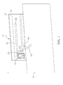
- FIG. 1 is a structural drawing of a communication electronic device with an antenna structure 1 according to a first exemplary embodiment of the present invention.
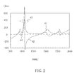
- FIG. 2 is a diagram illustrating the input impedance of the communication electronic device with the antenna structure 1 according to the first exemplary embodiment of the present invention.
- the communication electronic device with the antenna structure 1 comprises a ground element 10 and an antenna element 11.
- the antenna element 11 is disposed on a dielectric substrate 12, and comprises a first radiation portion 13, a second radiation portion 14 and a spiral metal line 15.
- a first end of the first radiation portion 13 is a feeding point 131 of the antenna element 11, the signal is fed through a coaxial line 16 connected thereto.
- a second end of the first radiation portion 13 is an open end 132.
- One end 141 of the second radiation portion 14 is electrically coupled to the ground element 10.
- a length of the second radiation portion 14 is greater than that of the first radiation portion 13.
- the second radiation portion 14 is extended around the open end 132 of the first radiation portion 13.
- a first end 151 of the spiral metal line 15 is electrically coupled to the first radiation portion 13.
- the spiral metal line 15 can contribute a parallel resonance 43 (as shown in FIG. 2 ) at a frequency outside a lower band 31 (shown in FIG. 5 ) of the antenna element 11.
- the parallel resonance 43 generates an additional resonant mode 312 (as shown in FIG. 5 ) in the lower band 31 such that an operating bandwidth of the antenna in the lower band 31 can be increased.
- the first radiation portion 13 is implemented using a monopole antenna.
- a second end 152 of the spiral metal line 15 is an open end and spirals inward.
- the spiral metal line 15 spirals in a rectangular shape.
- FIG. 3 is a structural drawing of a conventional communication electronic device with a conventional antenna structure 2 thereof.
- FIG. 4 is a diagram illustrating input impedance of the conventional communication electronic device with the conventional antenna structure 2.
- the communication electronic device and the antenna structure 2 comprise a ground element 20 and an antenna element 21.
- the antenna element 21 is disposed on a dielectric substrate 22, and comprises a first radiation portion 23 and a second radiation portion 24.
- a first end of the first radiation portion 23 is a feeding point 231 of the antenna element 21, and the signal is fed through a coaxial line 26 connected thereto.
- the second end of the first radiation portion 23 is an open end 232.
- the first radiation portion 23 can contribute a resonant mode (as shown in FIG. 3 ) at a higher band 32 of the antenna element 21.
- a first end 241 of the second radiation portion 24 is electrically coupled to the ground element 20.
- a length of the second radiation portion 24 is greater than that of the first radiation portion 23.
- the second radiation portion 24 is extended around the open end 232 of the first radiation portion 23.
- the second radiation portion 24 can contribute a resonant mode (e.g. the resonant mode 313 shown in FIG. 5 ) at a lower band 31 of the antenna element 21.
- the bandwidth of the resonant mode is narrow, which fails to cover multi-band operation.
- the antenna element 11 of the communication electronic device with the antenna structure 1 includes the spiral metal line 15. With the spiral metal line 15, a parallel resonance can be generated at a frequency outside the lower band of the antenna element 11. The parallel resonance will in turn generate a resonant mode in the lower band, which can be further combined with the original resonant mode of the second radiation portion, thereby increasing the operating bandwidth of the antenna element 11.
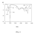
- FIG. 5 is a diagram illustrating return loss of the communication electronic device 1 as shown in FIG. 1 and the conventional communication electronic device 2 as shown in FIG. 3 .
- the first radiation portion 13 of the communication electronic device 1 generates at least one resonant mode in a second (higher frequency) operating band 32.
- the second radiation portion 14 of the communication electronic device 1 generates at least one resonant mode in the first (lower frequency) operating band 31.
- FIG. 2 is a diagram illustrating the input impedance of the communication electronic device with the antenna structure 1.
- FIG. 4 is a diagram illustrating the input impedance of the conventional communication electronic device with the antenna structure 2.
- FIG. 5 is a diagram illustrating return loss of the communication electronic device 1 of FIG. 1 and the conventional communication electronic device 2 of FIG. 3 .
- the input impedance of the communication electronic device 1 has a real part 41 and an imaginary part 42.
- the input impedance of the communication electronic device 2 has a real part 51 and an imaginary part 52.
- a length of the ground element 20 is about 150 mm and a width of the ground element 20 is about 200 mm; a length of the dielectric substrate 22 is about 40 mm, a width of the dielectric substrate 22 is about 12 mm and a thickness of the dielectric substrate 22 is about 0.8 mm.
- a length of the first radiation portion 23 is about 30 mm and a length of second radiation portion 24 is about 75 mm. The second radiation portion 24 can cause a quarter-wavelength resonant mode 313.
- the bandwidth of the resonant mode 313 will be narrow and fail to cover multi-band operation with the 6-dB return-loss definition (which is the design specification widely used for the mobile communication device antennas).
- the sizes of the elements are chosen as the similar sizes of the elements of the conventional communication electronic device 2 shown in FIG. 3 .
- a length of the spiral metal line 15 is about 60 mm.
- the second radiation portion 14 can cause the quarter-wavelength resonant mode 311 and the higher-order resonant mode.
- the spiral metal line 15 can contribute a parallel resonance 43 (having a center frequency at about 1.1 GHz) at a frequency outside the lower band 31 of the antenna element 11.
- the parallel resonance 43 generates an additional resonance around the resonant mode 311 (e.g. the zero imaginary part of the impedance as shown in FIG. 2 ), thereby generating a resonant mode 312.
- the resonant mode 312 and the resonant mode 311 generated by the second radiation portion 14 collectively generate the first (lower frequency) operating band (e.g. the operating band 31 shown in FIG. 5 ).
- the first radiation portion 13 can cause a quarter-wavelength resonant mode.
- the quarter-wavelength resonant mode and the higher-order resonant mode generated by the second radiation portion 14 collectively generate the second (higher frequency) operating band (e.g. the operating band 32 shown in FIG. 5 ).
- the first operating band 31 covers at least the dual-band operation of GSM850/900 (from about 824 to 960 MHz).
- the second operating band 32 covers at least the triple-band operation of GSM1800/1900/UMTS (from about 1710 to 2170 MHz).
- the operating bandwidth of the communication electronic device 1 is significantly increased by the spiral metal line 15, thereby allowing the first operating band 31 to achieve multi-band operation.
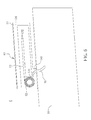
- FIG. 6 is a structural drawing of a communication electronic device with an antenna structure 6 thereof according to a second exemplary embodiment of the present invention.
- the antenna structure is basically similar to the antenna structure of the first exemplary embodiment.
- the difference between these two exemplary embodiments is that structures of the antenna element 61 and the spiral metal line 65 are changed.
- the spiral metal line 65 can spiral in circular shapes. Since the antenna structure of the second exemplary embodiment is similar to that of the first exemplary embodiment, effects of the second exemplary embodiment are also similar to those of the first exemplary embodiment.
- FIG. 7 is a structural drawing of a communication electronic device with an antenna structure 7 according to a third exemplary embodiment of the present invention.
- the antenna structure of the third exemplary embodiment is basically similar to the antenna structure of the first exemplary embodiment.
- the difference between the antenna structures of these two exemplary embodiments is that the position where the antenna element 71 and the spiral metal line 75 are electrically coupled is changed.
- the spiral metal line 75 is adjusted to determine the center frequency of the parallel resonance generated by the spiral metal line 75. Since the antenna structure of the third exemplary embodiment is similar to that of the first exemplary embodiment, effects of the third exemplary embodiment are also similar to those of the first exemplary embodiment.
Landscapes
- Engineering & Computer Science (AREA)
- Computer Networks & Wireless Communication (AREA)
- Details Of Aerials (AREA)
- Support Of Aerials (AREA)
Abstract
Description
- The present invention relates to a communication electronic device having a small-size planar antenna utilizing parallel resonance to generate multi-band operation according to the pre-characterizing clause of
Claim 1. - With the rapid development of mobile communication technologies and markets, wireless access capabilities are indispensable to portable communication electronic devices. In addition to wireless local area networks (WLAN), a wireless wide area network (WWAN) has been developed which is able to provide services over a wide coverage. Long term evolution (LTE) technology can provide higher data rates, thereby improving convenience and providing real time in wireless access when a portable communication electronic device is used. Slim-profile designs are also becoming more attractive in the communication electronic device market. Hence, it is critical to design a planar printed antenna that has the capability of covering multi-band operation for a slim mobile device.
-
U.S. Patent (No. 7978141 B2 ) entitled "Coupled-fed multi-band loop antenna" discloses a dual-band antenna used in a communication electronic device, wherein the antenna has two operating bands. This lower operating band of the antenna fails to cover multi-band operation. As a result, the antenna cannot cover all the lower operating bands in the WWAN or LTE system. - There is therefore a need for a communication electronic device, which has two wide operating bands. For example, the operating bands can cover the 824~960 MHz band as well as the 1710~2170 MHz band. To meet the needs of slim-profile design, the antenna element should also have the characteristics of planar structure and small size.
- This in mind, the invention aims at providing a communication electronic device having the advantages of small size, planar structure, and multi-band operation.
- This is achieved by providing an antenna structure according to
Claim 1. The antenna has a spiral metal line, which can increase an operating bandwidth of the antenna element. As the spiral metal line has a small size, it does not increase the size of the antenna structure. - The dependent claims pertain to corresponding further developments and improvements.
- As will be seen more clearly from the detailed description below, in an aspect of the present invention, a claimed communication electronic device has an antenna structure. The antenna structure comprises a ground element and an antenna element that is disposed on a dielectric substrate. The antenna element comprises a first radiation portion, a second radiation portion and a spiral metal line, wherein a first end of the first radiation portion is a feeding point of the antenna element, and a second end is an open end. One end of the second radiation portion is electrically coupled to the ground element. The second radiation portion is extended around the open end of the first radiation portion. A first end of the spiral metal line is electrically coupled to the first radiation portion. The spiral metal line contributes a parallel resonance at a frequency outside an operating band of the antenna element. The parallel resonance further contributes a resonant mode in the operating band, thereby increasing an operating bandwidth of the antenna element.
- In one exemplary embodiment, the second radiation portion of the antenna element generates a resonant mode at lower frequencies. The higher-order resonant mode of the second radiation portion can further combine with a resonant mode generated by the first radiation portion at higher frequencies to increase the operating bandwidth. Additionally, with the addition of the spiral metal line, the first end of the spiral metal line is electrically coupled to the first radiation portion, which generates a parallel resonance at a frequency outside the lower operating band of the antenna element. The parallel resonance will in turn generate a resonant mode in the lower operating band, which will be combined with the original resonant mode generated by the second radiation portion to increase the operating bandwidth of the antenna element.
- In one exemplary embodiment, the size of the antenna is only 12 x 40 mm2, and is able to cover the penta-band WWAN operation (824~960/1710~2170 MHz), thereby obtaining the advantages of small size, planar structure, and multi-band operation.
- In the following, the invention is further illustrated by way of example, taking reference to the following drawings. Thereof:
- FIG. 1
- is a structural drawing of a communication electronic device with an antenna structure according to a first exemplary embodiment of the present invention;
- FIG. 2
- is a diagram illustrating input impedance of the communication electronic device with the antenna structure;
- FIG. 3
- is a structural drawing of a conventional communication electronic device with a conventional antenna structure;
- FIG. 4
- is a diagram illustrating input impedance of the conventional communication electronic device with the conventional antenna structure;
- FIG. 5
- is a diagram illustrating return loss of the communication electronic device of
FIG. 1 and the conventional communication electronic device ofFIG. 3 ; - FIG. 6
- is a structural drawing of a communication electronic device with an antenna structure according to a second exemplary embodiment of the present invention; and
- FIG. 7
- is a structural drawing of a communication electronic device with an antenna structure according to a third exemplary embodiment of the present invention.
- The following description is of the best-contemplated mode of carrying out the present invention. A detailed description is given in the following embodiments with reference to the accompanying drawings.
- Certain terms are used throughout the following descriptions and claims to refer to particular system components. As one skilled in the art will appreciate, manufacturers may refer to a component by different names. This document does not intend to distinguish between components that differ in name but not differ in functionality. In the following discussion and in the claims, the terms "include", "including", "comprise", and "comprising" are used in an open-ended fashion, and thus should be interpreted to mean "including, but not limited to ..." The terms "couple" and "coupled" are intended to mean either an indirect or a direct electrical connection. Thus, if a first device couples to a second device, that connection may be through a direct electrical connection, or through an indirect electrical connection via other devices and connections.
- Please refer to
FIG. 1 in conjunction withFIG. 2 .FIG. 1 is a structural drawing of a communication electronic device with anantenna structure 1 according to a first exemplary embodiment of the present invention.FIG. 2 is a diagram illustrating the input impedance of the communication electronic device with theantenna structure 1 according to the first exemplary embodiment of the present invention. In the first exemplary embodiment, the communication electronic device with theantenna structure 1 comprises aground element 10 and anantenna element 11. Theantenna element 11 is disposed on adielectric substrate 12, and comprises afirst radiation portion 13, asecond radiation portion 14 and aspiral metal line 15. A first end of thefirst radiation portion 13 is afeeding point 131 of theantenna element 11, the signal is fed through acoaxial line 16 connected thereto. Additionally, a second end of thefirst radiation portion 13 is anopen end 132. Oneend 141 of thesecond radiation portion 14 is electrically coupled to theground element 10. A length of thesecond radiation portion 14 is greater than that of thefirst radiation portion 13. Thesecond radiation portion 14 is extended around theopen end 132 of thefirst radiation portion 13. Afirst end 151 of thespiral metal line 15 is electrically coupled to thefirst radiation portion 13. Thespiral metal line 15 can contribute a parallel resonance 43 (as shown inFIG. 2 ) at a frequency outside a lower band 31 (shown inFIG. 5 ) of theantenna element 11. Theparallel resonance 43 generates an additional resonant mode 312 (as shown inFIG. 5 ) in thelower band 31 such that an operating bandwidth of the antenna in thelower band 31 can be increased. It should be noted that, in this embodiment, thefirst radiation portion 13 is implemented using a monopole antenna. - Further, in this embodiment, a
second end 152 of thespiral metal line 15 is an open end and spirals inward. Thespiral metal line 15 spirals in a rectangular shape. These features should not be considered as limitations of the present invention. Additionally, in this embodiment, the length of thespiral metal line 15 is close to one quarter of a wavelength of the center frequency of the parallel resonance 43 (as shown inFIG. 2 ). - Please refer to
FIG. 3 in conjunction withFIG. 4 .FIG. 3 is a structural drawing of a conventional communication electronic device with aconventional antenna structure 2 thereof.FIG. 4 is a diagram illustrating input impedance of the conventional communication electronic device with theconventional antenna structure 2. As shown inFIG. 3 , the communication electronic device and theantenna structure 2 comprise aground element 20 and anantenna element 21. Theantenna element 21 is disposed on adielectric substrate 22, and comprises afirst radiation portion 23 and asecond radiation portion 24. A first end of thefirst radiation portion 23 is afeeding point 231 of theantenna element 21, and the signal is fed through a coaxial line 26 connected thereto. The second end of thefirst radiation portion 23 is anopen end 232. Thefirst radiation portion 23 can contribute a resonant mode (as shown inFIG. 3 ) at ahigher band 32 of theantenna element 21. Afirst end 241 of thesecond radiation portion 24 is electrically coupled to theground element 20. A length of thesecond radiation portion 24 is greater than that of thefirst radiation portion 23. Thesecond radiation portion 24 is extended around theopen end 232 of thefirst radiation portion 23. Also, thesecond radiation portion 24 can contribute a resonant mode (e.g. theresonant mode 313 shown inFIG. 5 ) at alower band 31 of theantenna element 21. The bandwidth of the resonant mode is narrow, which fails to cover multi-band operation. - The difference between the communication electronic device with the
antenna structure 1 ofFIG. 1 and the conventional communication electronic device with theconventional antenna structure 2 is that theantenna element 11 of the communication electronic device with theantenna structure 1 includes thespiral metal line 15. With thespiral metal line 15, a parallel resonance can be generated at a frequency outside the lower band of theantenna element 11. The parallel resonance will in turn generate a resonant mode in the lower band, which can be further combined with the original resonant mode of the second radiation portion, thereby increasing the operating bandwidth of theantenna element 11. - Please refer to
FIG. 5 , which is a diagram illustrating return loss of the communicationelectronic device 1 as shown inFIG. 1 and the conventional communicationelectronic device 2 as shown inFIG. 3 . In the first exemplary embodiment, thefirst radiation portion 13 of the communicationelectronic device 1 generates at least one resonant mode in a second (higher frequency) operatingband 32. Thesecond radiation portion 14 of the communicationelectronic device 1 generates at least one resonant mode in the first (lower frequency) operatingband 31. - Please refer to
FIG. 2 in conjunction withFIG. 3 andFIG. 5 .FIG. 2 is a diagram illustrating the input impedance of the communication electronic device with theantenna structure 1.FIG. 4 is a diagram illustrating the input impedance of the conventional communication electronic device with theantenna structure 2.FIG. 5 is a diagram illustrating return loss of the communicationelectronic device 1 ofFIG. 1 and the conventional communicationelectronic device 2 ofFIG. 3 . As shown inFIG. 2 , the input impedance of the communicationelectronic device 1 has areal part 41 and animaginary part 42. As shown inFIG. 4 , the input impedance of the communicationelectronic device 2 has areal part 51 and animaginary part 52. - In the communication device shown in
FIG. 3 , a length of theground element 20 is about 150 mm and a width of theground element 20 is about 200 mm; a length of thedielectric substrate 22 is about 40 mm, a width of thedielectric substrate 22 is about 12 mm and a thickness of thedielectric substrate 22 is about 0.8 mm. A length of thefirst radiation portion 23 is about 30 mm and a length ofsecond radiation portion 24 is about 75 mm. Thesecond radiation portion 24 can cause a quarter-wavelengthresonant mode 313. Since the impedance of theresonant mode 313 has a larger real part, the bandwidth of theresonant mode 313 will be narrow and fail to cover multi-band operation with the 6-dB return-loss definition (which is the design specification widely used for the mobile communication device antennas). In the communicationelectronic device 1 as shown inFIG. 1 , the sizes of the elements are chosen as the similar sizes of the elements of the conventional communicationelectronic device 2 shown inFIG. 3 . Further, a length of thespiral metal line 15 is about 60 mm. Thesecond radiation portion 14 can cause the quarter-wavelengthresonant mode 311 and the higher-order resonant mode. Thespiral metal line 15 can contribute a parallel resonance 43 (having a center frequency at about 1.1 GHz) at a frequency outside thelower band 31 of theantenna element 11. Theparallel resonance 43 generates an additional resonance around the resonant mode 311 (e.g. the zero imaginary part of the impedance as shown inFIG. 2 ), thereby generating aresonant mode 312. Theresonant mode 312 and theresonant mode 311 generated by thesecond radiation portion 14 collectively generate the first (lower frequency) operating band (e.g. the operatingband 31 shown inFIG. 5 ). Thefirst radiation portion 13 can cause a quarter-wavelength resonant mode. The quarter-wavelength resonant mode and the higher-order resonant mode generated by thesecond radiation portion 14 collectively generate the second (higher frequency) operating band (e.g. the operatingband 32 shown inFIG. 5 ). Under the definition of 6 dB return loss, thefirst operating band 31 covers at least the dual-band operation of GSM850/900 (from about 824 to 960 MHz). Thesecond operating band 32 covers at least the triple-band operation of GSM1800/1900/UMTS (from about 1710 to 2170 MHz). Compared to the conventional communicationelectronic device 2, the operating bandwidth of the communicationelectronic device 1 is significantly increased by thespiral metal line 15, thereby allowing thefirst operating band 31 to achieve multi-band operation. - Please refer to
FIG. 6 , which is a structural drawing of a communication electronic device with anantenna structure 6 thereof according to a second exemplary embodiment of the present invention. In the second exemplary embodiment, the antenna structure is basically similar to the antenna structure of the first exemplary embodiment. The difference between these two exemplary embodiments is that structures of theantenna element 61 and thespiral metal line 65 are changed. In the second exemplary embodiment, thespiral metal line 65 can spiral in circular shapes. Since the antenna structure of the second exemplary embodiment is similar to that of the first exemplary embodiment, effects of the second exemplary embodiment are also similar to those of the first exemplary embodiment. - Please refer to
FIG. 7 , which is a structural drawing of a communication electronic device with anantenna structure 7 according to a third exemplary embodiment of the present invention. The antenna structure of the third exemplary embodiment is basically similar to the antenna structure of the first exemplary embodiment. The difference between the antenna structures of these two exemplary embodiments is that the position where theantenna element 71 and thespiral metal line 75 are electrically coupled is changed. Also, thespiral metal line 75 is adjusted to determine the center frequency of the parallel resonance generated by thespiral metal line 75. Since the antenna structure of the third exemplary embodiment is similar to that of the first exemplary embodiment, effects of the third exemplary embodiment are also similar to those of the first exemplary embodiment. - All combinations and sub-combinations of the above-described features also belong to the invention.
Claims (9)
- An antenna structure, comprising:a ground element (10); andan antenna element (11, 61, 71), disposed on a dielectric substrate (12),comprising:a first radiation portion (13), having a first end (131) as a feeding point of the antenna element (11, 61, 71), and a second end (132) as an open end;a second radiation portion (14), having one end (141) electrically coupled to the ground element (10), wherein a length of the second radiation portion (14) is greater than that of the first radiation portion (13), and the second radiation portion (14) is extended around the open end (132) of the first radiation portion (13); and
characterized by:a spiral metal line (15, 65, 75), having a first end (141) electrically coupled to the first radiation portion (13), wherein the spiral metal line (15, 65, 75) contributes a parallel resonance (43) at a frequency outside an operating band of the antenna element (11, 61, 71), and the parallel resonance (43) contributes a resonant mode in the operating band to increase an operating bandwidth of the antenna element (11, 61, 71). - The antenna structure of claim 1, characterized in that the first radiation portion (13) is a monopole antenna.
- The antenna structure of claim 1, characterized in that a second end (152) of the spiral metal line (15, 65, 75) is an open end and spirals inward.
- The antenna structure of claim 1, characterized in that the spiral metal line (15, 65, 75) spirals in rectangular shapes or in circular shapes.
- The antenna structure of claim 1, characterized in that the spiral metal line (15, 65, 75) is disposed between the first radiation portion (13) and the second radiation portion (14).
- The antenna structure of claim 1, characterized in that a length of the spiral metal line (15, 65, 75) is close to one quarter of a wavelength of a center frequency of the parallel resonance (43).
- The antenna structure of claim 1, characterized in that the antenna element (11, 61, 71) has a first operating band (31) and a second operating band (32), and the first operating band (31) covers about 824 to 960 MHz, and the second operating band (32) covers about 1710 to 2170 MHz.
- The antenna structure of claim 1, characterized in that the second radiation portion (14) contributes at least a first resonant mode (312) in the first operating band (31), and the first radiation portion (13) contributes at least a second resonant mode (311, 313) in the second operating band (32).
- The antenna structure of claim 1, characterized in that the antenna structure is disposed in a communication electronic device (1, 6, 7).
Applications Claiming Priority (1)
| Application Number | Priority Date | Filing Date | Title |
|---|---|---|---|
| TW100148862A TWI488358B (en) | 2011-12-27 | 2011-12-27 | Communication electronic device and antenna structure thereof |
Publications (2)
| Publication Number | Publication Date |
|---|---|
| EP2610962A2 true EP2610962A2 (en) | 2013-07-03 |
| EP2610962A3 EP2610962A3 (en) | 2013-10-23 |
Family
ID=46197041
Family Applications (1)
| Application Number | Title | Priority Date | Filing Date |
|---|---|---|---|
| EP12168895.6A Withdrawn EP2610962A3 (en) | 2011-12-27 | 2012-05-22 | Communication electronic device and antenna structure thereof |
Country Status (3)
| Country | Link |
|---|---|
| US (1) | US8922449B2 (en) |
| EP (1) | EP2610962A3 (en) |
| TW (1) | TWI488358B (en) |
Cited By (1)
| Publication number | Priority date | Publication date | Assignee | Title |
|---|---|---|---|---|
| WO2017001937A1 (en) * | 2015-01-07 | 2017-01-05 | Galtronics Corporation Ltd. | Compact antenna structure |
Families Citing this family (14)
| Publication number | Priority date | Publication date | Assignee | Title |
|---|---|---|---|---|
| CN104577303A (en) * | 2013-10-17 | 2015-04-29 | 启碁科技股份有限公司 | Antenna with a shield |
| TWI451629B (en) | 2013-11-04 | 2014-09-01 | Quanta Comp Inc | Antenna structure |
| TWI509883B (en) * | 2013-12-06 | 2015-11-21 | Univ Nat Kaohsiung Marine | Multi-mode monopole antenna with planar strips |
| CN104795624A (en) * | 2014-01-17 | 2015-07-22 | 台湾立讯精密有限公司 | Full frequency band antenna |
| TWI501464B (en) * | 2014-03-05 | 2015-09-21 | Quanta Comp Inc | Mobile device |
| CN206907920U (en) * | 2016-12-14 | 2018-01-19 | 深圳市道通智能航空技术有限公司 | A kind of unmanned plane of dual-band microstrip antenna and the application antenna |
| CN112821037B (en) | 2019-11-15 | 2022-09-02 | 英业达科技有限公司 | Multi-frequency antenna |
| TWI725642B (en) * | 2019-11-29 | 2021-04-21 | 英業達股份有限公司 | Multi-band antenna |
| CN112968270B (en) * | 2019-12-13 | 2022-09-23 | 华为技术有限公司 | Dual-frequency antenna and communication equipment |
| TWI723833B (en) * | 2020-04-01 | 2021-04-01 | 啟碁科技股份有限公司 | Antenna structure |
| CN114069207B (en) * | 2020-07-29 | 2023-08-22 | 北京小米移动软件有限公司 | Antenna structure and electronics |
| CN112736454B (en) * | 2020-12-25 | 2023-04-07 | RealMe重庆移动通信有限公司 | Antenna assembly and electronic equipment |
| CN115603036B (en) * | 2022-09-08 | 2025-07-11 | 昆山睿翔讯通通信技术有限公司 | Mobile terminal antenna and mobile terminal |
| US20250030150A1 (en) * | 2022-09-08 | 2025-01-23 | Kunshan Innowave Communication Technology Co., Ltd. | Antenna for mobile terminal, and mobile terminal |
Citations (1)
| Publication number | Priority date | Publication date | Assignee | Title |
|---|---|---|---|---|
| US7978141B2 (en) | 2008-05-05 | 2011-07-12 | Acer Incorporated | Couple-fed multi-band loop antenna |
Family Cites Families (7)
| Publication number | Priority date | Publication date | Assignee | Title |
|---|---|---|---|---|
| WO2002013312A1 (en) | 2000-08-04 | 2002-02-14 | Matsushita Electric Industrial Co., Ltd. | Antenna device and radio communication device comprising the same |
| EP1547194A1 (en) * | 2002-09-10 | 2005-06-29 | Fractus, S.A. | Coupled multiband antennas |
| US20060197538A1 (en) * | 2005-03-07 | 2006-09-07 | Nokia Corporation | Self-test method for antennas |
| US7760146B2 (en) * | 2005-03-24 | 2010-07-20 | Nokia Corporation | Internal digital TV antennas for hand-held telecommunications device |
| WO2007128340A1 (en) * | 2006-05-04 | 2007-11-15 | Fractus, S.A. | Wireless portable device including internal broadcast receiver |
| US8618990B2 (en) * | 2011-04-13 | 2013-12-31 | Pulse Finland Oy | Wideband antenna and methods |
| KR101480555B1 (en) * | 2008-06-19 | 2015-01-09 | 삼성전자주식회사 | Antenna device for portable terminal |
-
2011
- 2011-12-27 TW TW100148862A patent/TWI488358B/en active
-
2012
- 2012-04-18 US US13/449,318 patent/US8922449B2/en active Active
- 2012-05-22 EP EP12168895.6A patent/EP2610962A3/en not_active Withdrawn
Patent Citations (1)
| Publication number | Priority date | Publication date | Assignee | Title |
|---|---|---|---|---|
| US7978141B2 (en) | 2008-05-05 | 2011-07-12 | Acer Incorporated | Couple-fed multi-band loop antenna |
Cited By (2)
| Publication number | Priority date | Publication date | Assignee | Title |
|---|---|---|---|---|
| WO2017001937A1 (en) * | 2015-01-07 | 2017-01-05 | Galtronics Corporation Ltd. | Compact antenna structure |
| CN107534211A (en) * | 2015-01-07 | 2018-01-02 | 盖尔创尼克斯有限公司 | Compact antenna structure |
Also Published As
| Publication number | Publication date |
|---|---|
| EP2610962A3 (en) | 2013-10-23 |
| US8922449B2 (en) | 2014-12-30 |
| TW201328016A (en) | 2013-07-01 |
| TWI488358B (en) | 2015-06-11 |
| US20130162494A1 (en) | 2013-06-27 |
Similar Documents
| Publication | Publication Date | Title |
|---|---|---|
| US8922449B2 (en) | Communication electronic device and antenna structure thereof | |
| US10819031B2 (en) | Printed circuit board antenna and terminal | |
| US6614400B2 (en) | Antenna | |
| US7616158B2 (en) | Multi mode antenna system | |
| US6552686B2 (en) | Internal multi-band antenna with improved radiation efficiency | |
| CN102075205B (en) | Mobile communication device | |
| CN1173432C (en) | Ground extension structure for connection to a ground device in an antenna system, and antenna system and mobile antenna device having such a ground structure | |
| US6734825B1 (en) | Miniature built-in multiple frequency band antenna | |
| US9276320B2 (en) | Multi-band antenna | |
| EP2246935A1 (en) | Multi-loop antenna structure and hand-held electronic device using the same | |
| EP2511978B1 (en) | Mobile communication device and antenna structure therein | |
| EP2381529B1 (en) | Communications structures including antennas with separate antenna branches coupled to feed and ground conductors | |
| US8593354B2 (en) | Multi-band antenna | |
| US20080231532A1 (en) | Multi-band slot-strip antenna | |
| EP2509158B1 (en) | Communication electronic device and antenna structure thereof | |
| EP2575207B1 (en) | Communication electronic device and antenna structure thereof | |
| WO2007107101A1 (en) | Single feed internal antenna with multi-band for mobile communication terminals | |
| US20130225234A1 (en) | Mobile device and wideband antenna structure therein | |
| CN102099962A (en) | Antenna arrangement | |
| EP1852939A1 (en) | Portable wireless device | |
| CN100468861C (en) | Multiband Radio Antenna | |
| EP1678783B1 (en) | Multi-band antennas and radio apparatus incorporating the same | |
| CN101283478A (en) | Antenna structure provided with notch filter | |
| Elfergani et al. | Dual-band printed folded dipole balanced antenna for 700/2600MHz LTE bands | |
| CN1885613B (en) | Inversed-F type antenna |
Legal Events
| Date | Code | Title | Description |
|---|---|---|---|
| PUAI | Public reference made under article 153(3) epc to a published international application that has entered the european phase |
Free format text: ORIGINAL CODE: 0009012 |
|
| AK | Designated contracting states |
Kind code of ref document: A2 Designated state(s): AL AT BE BG CH CY CZ DE DK EE ES FI FR GB GR HR HU IE IS IT LI LT LU LV MC MK MT NL NO PL PT RO RS SE SI SK SM TR |
|
| AX | Request for extension of the european patent |
Extension state: BA ME |
|
| PUAL | Search report despatched |
Free format text: ORIGINAL CODE: 0009013 |
|
| AK | Designated contracting states |
Kind code of ref document: A3 Designated state(s): AL AT BE BG CH CY CZ DE DK EE ES FI FR GB GR HR HU IE IS IT LI LT LU LV MC MK MT NL NO PL PT RO RS SE SI SK SM TR |
|
| AX | Request for extension of the european patent |
Extension state: BA ME |
|
| RIC1 | Information provided on ipc code assigned before grant |
Ipc: H01Q 1/38 20060101ALI20130913BHEP Ipc: H01Q 1/24 20060101AFI20130913BHEP Ipc: H01Q 9/40 20060101ALI20130913BHEP Ipc: H01Q 5/00 20060101ALI20130913BHEP Ipc: H01Q 9/42 20060101ALI20130913BHEP |
|
| STAA | Information on the status of an ep patent application or granted ep patent |
Free format text: STATUS: THE APPLICATION IS DEEMED TO BE WITHDRAWN |
|
| 18D | Application deemed to be withdrawn |
Effective date: 20140424 |