EP2610923A2 - Photoconductive antenna, terahertz wave generating device, camera, imaging device, and measuring device - Google Patents
Photoconductive antenna, terahertz wave generating device, camera, imaging device, and measuring device Download PDFInfo
- Publication number
- EP2610923A2 EP2610923A2 EP12199071.7A EP12199071A EP2610923A2 EP 2610923 A2 EP2610923 A2 EP 2610923A2 EP 12199071 A EP12199071 A EP 12199071A EP 2610923 A2 EP2610923 A2 EP 2610923A2
- Authority
- EP
- European Patent Office
- Prior art keywords
- semiconductor layer
- type semiconductor
- photoconductive antenna
- layer
- terahertz wave
- Prior art date
- Legal status (The legal status is an assumption and is not a legal conclusion. Google has not performed a legal analysis and makes no representation as to the accuracy of the status listed.)
- Withdrawn
Links
- 238000003384 imaging method Methods 0.000 title claims description 22
- 239000004065 semiconductor Substances 0.000 claims abstract description 261
- 239000000463 material Substances 0.000 claims abstract description 48
- 238000003475 lamination Methods 0.000 claims abstract description 18
- 239000000758 substrate Substances 0.000 claims description 37
- 239000012535 impurity Substances 0.000 claims description 21
- 238000001514 detection method Methods 0.000 claims description 20
- 150000001875 compounds Chemical class 0.000 claims description 6
- 238000005253 cladding Methods 0.000 description 21
- 239000000126 substance Substances 0.000 description 17
- 238000010586 diagram Methods 0.000 description 14
- 238000009413 insulation Methods 0.000 description 10
- 230000006835 compression Effects 0.000 description 9
- 238000007906 compression Methods 0.000 description 9
- 230000000694 effects Effects 0.000 description 9
- 238000005530 etching Methods 0.000 description 9
- 238000012545 processing Methods 0.000 description 9
- 230000005540 biological transmission Effects 0.000 description 6
- 238000009826 distribution Methods 0.000 description 6
- 229910001218 Gallium arsenide Inorganic materials 0.000 description 5
- VYPSYNLAJGMNEJ-UHFFFAOYSA-N Silicium dioxide Chemical compound O=[Si]=O VYPSYNLAJGMNEJ-UHFFFAOYSA-N 0.000 description 5
- OMOVVBIIQSXZSZ-UHFFFAOYSA-N [6-(4-acetyloxy-5,9a-dimethyl-2,7-dioxo-4,5a,6,9-tetrahydro-3h-pyrano[3,4-b]oxepin-5-yl)-5-formyloxy-3-(furan-3-yl)-3a-methyl-7-methylidene-1a,2,3,4,5,6-hexahydroindeno[1,7a-b]oxiren-4-yl] 2-hydroxy-3-methylpentanoate Chemical compound CC12C(OC(=O)C(O)C(C)CC)C(OC=O)C(C3(C)C(CC(=O)OC4(C)COC(=O)CC43)OC(C)=O)C(=C)C32OC3CC1C=1C=COC=1 OMOVVBIIQSXZSZ-UHFFFAOYSA-N 0.000 description 5
- 238000010521 absorption reaction Methods 0.000 description 5
- 238000004519 manufacturing process Methods 0.000 description 5
- GWEVSGVZZGPLCZ-UHFFFAOYSA-N Titan oxide Chemical compound O=[Ti]=O GWEVSGVZZGPLCZ-UHFFFAOYSA-N 0.000 description 4
- -1 borazine compound Chemical class 0.000 description 4
- 230000003247 decreasing effect Effects 0.000 description 4
- 229920005989 resin Polymers 0.000 description 4
- 239000011347 resin Substances 0.000 description 4
- 238000000701 chemical imaging Methods 0.000 description 3
- 239000003989 dielectric material Substances 0.000 description 3
- 239000006185 dispersion Substances 0.000 description 3
- 238000005259 measurement Methods 0.000 description 3
- 230000000704 physical effect Effects 0.000 description 3
- 229910000980 Aluminium gallium arsenide Inorganic materials 0.000 description 2
- JBRZTFJDHDCESZ-UHFFFAOYSA-N AsGa Chemical compound [As]#[Ga] JBRZTFJDHDCESZ-UHFFFAOYSA-N 0.000 description 2
- YCKRFDGAMUMZLT-UHFFFAOYSA-N Fluorine atom Chemical compound [F] YCKRFDGAMUMZLT-UHFFFAOYSA-N 0.000 description 2
- 229910000673 Indium arsenide Inorganic materials 0.000 description 2
- GPXJNWSHGFTCBW-UHFFFAOYSA-N Indium phosphide Chemical compound [In]#P GPXJNWSHGFTCBW-UHFFFAOYSA-N 0.000 description 2
- 239000004642 Polyimide Substances 0.000 description 2
- 239000006096 absorbing agent Substances 0.000 description 2
- 230000004888 barrier function Effects 0.000 description 2
- UMIVXZPTRXBADB-UHFFFAOYSA-N benzocyclobutene Chemical class C1=CC=C2CCC2=C1 UMIVXZPTRXBADB-UHFFFAOYSA-N 0.000 description 2
- 229910052681 coesite Inorganic materials 0.000 description 2
- 238000005260 corrosion Methods 0.000 description 2
- 230000007797 corrosion Effects 0.000 description 2
- 229910052906 cristobalite Inorganic materials 0.000 description 2
- KPUWHANPEXNPJT-UHFFFAOYSA-N disiloxane Chemical class [SiH3]O[SiH3] KPUWHANPEXNPJT-UHFFFAOYSA-N 0.000 description 2
- 229910052731 fluorine Inorganic materials 0.000 description 2
- 239000011737 fluorine Substances 0.000 description 2
- 230000006870 function Effects 0.000 description 2
- 239000011521 glass Substances 0.000 description 2
- WPYVAWXEWQSOGY-UHFFFAOYSA-N indium antimonide Chemical compound [Sb]#[In] WPYVAWXEWQSOGY-UHFFFAOYSA-N 0.000 description 2
- RPQDHPTXJYYUPQ-UHFFFAOYSA-N indium arsenide Chemical compound [In]#[As] RPQDHPTXJYYUPQ-UHFFFAOYSA-N 0.000 description 2
- 230000001678 irradiating effect Effects 0.000 description 2
- MRELNEQAGSRDBK-UHFFFAOYSA-N lanthanum(3+);oxygen(2-) Chemical compound [O-2].[O-2].[O-2].[La+3].[La+3] MRELNEQAGSRDBK-UHFFFAOYSA-N 0.000 description 2
- 238000000034 method Methods 0.000 description 2
- 229920001721 polyimide Polymers 0.000 description 2
- 229910052710 silicon Inorganic materials 0.000 description 2
- 239000000377 silicon dioxide Substances 0.000 description 2
- 238000001228 spectrum Methods 0.000 description 2
- 229910052682 stishovite Inorganic materials 0.000 description 2
- 229910052905 tridymite Inorganic materials 0.000 description 2
- 239000004698 Polyethylene Substances 0.000 description 1
- 238000004458 analytical method Methods 0.000 description 1
- 239000000470 constituent Substances 0.000 description 1
- 230000007423 decrease Effects 0.000 description 1
- 239000003814 drug Substances 0.000 description 1
- 229940079593 drug Drugs 0.000 description 1
- 230000009977 dual effect Effects 0.000 description 1
- 230000005684 electric field Effects 0.000 description 1
- 230000005284 excitation Effects 0.000 description 1
- 238000005187 foaming Methods 0.000 description 1
- 229910052735 hafnium Inorganic materials 0.000 description 1
- 229910000449 hafnium oxide Inorganic materials 0.000 description 1
- WIHZLLGSGQNAGK-UHFFFAOYSA-N hafnium(4+);oxygen(2-) Chemical compound [O-2].[O-2].[Hf+4] WIHZLLGSGQNAGK-UHFFFAOYSA-N 0.000 description 1
- 239000011159 matrix material Substances 0.000 description 1
- 238000012986 modification Methods 0.000 description 1
- 230000004048 modification Effects 0.000 description 1
- ZKATWMILCYLAPD-UHFFFAOYSA-N niobium pentoxide Inorganic materials O=[Nb](=O)O[Nb](=O)=O ZKATWMILCYLAPD-UHFFFAOYSA-N 0.000 description 1
- URLJKFSTXLNXLG-UHFFFAOYSA-N niobium(5+);oxygen(2-) Chemical compound [O-2].[O-2].[O-2].[O-2].[O-2].[Nb+5].[Nb+5] URLJKFSTXLNXLG-UHFFFAOYSA-N 0.000 description 1
- 238000009659 non-destructive testing Methods 0.000 description 1
- 230000003287 optical effect Effects 0.000 description 1
- SIWVEOZUMHYXCS-UHFFFAOYSA-N oxo(oxoyttriooxy)yttrium Chemical compound O=[Y]O[Y]=O SIWVEOZUMHYXCS-UHFFFAOYSA-N 0.000 description 1
- 229920000573 polyethylene Polymers 0.000 description 1
- 239000010453 quartz Substances 0.000 description 1
- 239000010703 silicon Substances 0.000 description 1
- 239000007787 solid Substances 0.000 description 1
- 238000004611 spectroscopical analysis Methods 0.000 description 1
- 239000004408 titanium dioxide Substances 0.000 description 1
- OGIDPMRJRNCKJF-UHFFFAOYSA-N titanium oxide Inorganic materials [Ti]=O OGIDPMRJRNCKJF-UHFFFAOYSA-N 0.000 description 1
- 229910052725 zinc Inorganic materials 0.000 description 1
Images





Classifications
-
- H—ELECTRICITY
- H01—ELECTRIC ELEMENTS
- H01Q—ANTENNAS, i.e. RADIO AERIALS
- H01Q1/00—Details of, or arrangements associated with, antennas
- H01Q1/36—Structural form of radiating elements, e.g. cone, spiral, umbrella; Particular materials used therewith
- H01Q1/38—Structural form of radiating elements, e.g. cone, spiral, umbrella; Particular materials used therewith formed by a conductive layer on an insulating support
-
- H—ELECTRICITY
- H10—SEMICONDUCTOR DEVICES; ELECTRIC SOLID-STATE DEVICES NOT OTHERWISE PROVIDED FOR
- H10H—INORGANIC LIGHT-EMITTING SEMICONDUCTOR DEVICES HAVING POTENTIAL BARRIERS
- H10H20/00—Individual inorganic light-emitting semiconductor devices having potential barriers, e.g. light-emitting diodes [LED]
-
- H—ELECTRICITY
- H01—ELECTRIC ELEMENTS
- H01Q—ANTENNAS, i.e. RADIO AERIALS
- H01Q1/00—Details of, or arrangements associated with, antennas
- H01Q1/36—Structural form of radiating elements, e.g. cone, spiral, umbrella; Particular materials used therewith
-
- H—ELECTRICITY
- H01—ELECTRIC ELEMENTS
- H01Q—ANTENNAS, i.e. RADIO AERIALS
- H01Q23/00—Antennas with active circuits or circuit elements integrated within them or attached to them
-
- H—ELECTRICITY
- H01—ELECTRIC ELEMENTS
- H01S—DEVICES USING THE PROCESS OF LIGHT AMPLIFICATION BY STIMULATED EMISSION OF RADIATION [LASER] TO AMPLIFY OR GENERATE LIGHT; DEVICES USING STIMULATED EMISSION OF ELECTROMAGNETIC RADIATION IN WAVE RANGES OTHER THAN OPTICAL
- H01S1/00—Masers, i.e. devices using stimulated emission of electromagnetic radiation in the microwave range
-
- H—ELECTRICITY
- H10—SEMICONDUCTOR DEVICES; ELECTRIC SOLID-STATE DEVICES NOT OTHERWISE PROVIDED FOR
- H10F—INORGANIC SEMICONDUCTOR DEVICES SENSITIVE TO INFRARED RADIATION, LIGHT, ELECTROMAGNETIC RADIATION OF SHORTER WAVELENGTH OR CORPUSCULAR RADIATION
- H10F30/00—Individual radiation-sensitive semiconductor devices in which radiation controls the flow of current through the devices, e.g. photodetectors
- H10F30/10—Individual radiation-sensitive semiconductor devices in which radiation controls the flow of current through the devices, e.g. photodetectors the devices being sensitive to infrared radiation, visible or ultraviolet radiation, and having no potential barriers, e.g. photoresistors
-
- H—ELECTRICITY
- H10—SEMICONDUCTOR DEVICES; ELECTRIC SOLID-STATE DEVICES NOT OTHERWISE PROVIDED FOR
- H10F—INORGANIC SEMICONDUCTOR DEVICES SENSITIVE TO INFRARED RADIATION, LIGHT, ELECTROMAGNETIC RADIATION OF SHORTER WAVELENGTH OR CORPUSCULAR RADIATION
- H10F30/00—Individual radiation-sensitive semiconductor devices in which radiation controls the flow of current through the devices, e.g. photodetectors
- H10F30/20—Individual radiation-sensitive semiconductor devices in which radiation controls the flow of current through the devices, e.g. photodetectors the devices having potential barriers, e.g. phototransistors
- H10F30/21—Individual radiation-sensitive semiconductor devices in which radiation controls the flow of current through the devices, e.g. photodetectors the devices having potential barriers, e.g. phototransistors the devices being sensitive to infrared, visible or ultraviolet radiation
- H10F30/22—Individual radiation-sensitive semiconductor devices in which radiation controls the flow of current through the devices, e.g. photodetectors the devices having potential barriers, e.g. phototransistors the devices being sensitive to infrared, visible or ultraviolet radiation the devices having only one potential barrier, e.g. photodiodes
- H10F30/223—Individual radiation-sensitive semiconductor devices in which radiation controls the flow of current through the devices, e.g. photodetectors the devices having potential barriers, e.g. phototransistors the devices being sensitive to infrared, visible or ultraviolet radiation the devices having only one potential barrier, e.g. photodiodes the potential barrier being a PIN barrier
-
- H—ELECTRICITY
- H10—SEMICONDUCTOR DEVICES; ELECTRIC SOLID-STATE DEVICES NOT OTHERWISE PROVIDED FOR
- H10F—INORGANIC SEMICONDUCTOR DEVICES SENSITIVE TO INFRARED RADIATION, LIGHT, ELECTROMAGNETIC RADIATION OF SHORTER WAVELENGTH OR CORPUSCULAR RADIATION
- H10F55/00—Radiation-sensitive semiconductor devices covered by groups H10F10/00, H10F19/00 or H10F30/00 being structurally associated with electric light sources and electrically or optically coupled thereto
- H10F55/20—Radiation-sensitive semiconductor devices covered by groups H10F10/00, H10F19/00 or H10F30/00 being structurally associated with electric light sources and electrically or optically coupled thereto wherein the electric light source controls the radiation-sensitive semiconductor devices, e.g. optocouplers
Definitions
- the present invention relates to a photoconductive antenna, a terahertz wave generating device, a camera, an imaging device, and a measuring device.
- Terahertz waves which are electromagnetic waves with frequencies of 100 GHz or greater and 30 THz or less. Terahertz waves can be used in various forms of measurement and non-destructive testing such as imaging and spectrometry.
- the terahertz wave generating device that generates these terahertz waves has a light source device that generates light pulses (pulsed light) having pulse widths at the approximately sub picosecond level (several hundred femtoseconds) and a photoconductive antenna that generates terahertz waves by irradiating light pulses generated by the light pulse generator.
- the photoconductive antenna for example, disclosed in Japanese Laid-Open Patent Application Publication No. 2007-300022 is a terahertz wave generating device (photoconductive antenna) having a laminated body (pin structure) for which an n type semiconductor layer, an i type semiconductor layer, and a p type semiconductor layer are laminated in that order.
- photoconductive antenna when light pulses are irradiated on the p type semiconductor layer via an aperture formed on an electrode provided on the p type semiconductor layer, terahertz waves are emitted radially from the entire side surface of the i type semiconductor layer.
- An object of the present invention is to provide a photoconductive antenna, a terahertz wave generating device, a camera, an imaging device, and a measuring device capable of generating terahertz waves with better efficiency than the prior art.
- a photoconductive antenna is adapted to generate terahertz waves when irradiated by pulsed light.
- the photoconductive antenna includes a first conductive layer, a second conductive layer, a semiconductor layer, a first electrode and a second electrode.
- the first conductive layer is made of a semiconductor material containing a first conductive type impurity.
- the second conductive layer is made of a semiconductor material containing a second conductive type impurity different from the first conductive type impurity.
- the semiconductor layer is positioned between the first conductive layer and the second conductive layer, and made of a semiconductor material having a carrier density that is lower than a carrier density of the semiconductor material of the first conductive layer or a carrier density of the semiconductor material of the second conductive layer.
- the first electrode is electrically connected to the first conductive layer.
- the second electrode is electrically connected to the second conductive layer.
- the semiconductor layer includes an incidence surface through which the pulsed light enters the semiconductor layer, and an emission surface from which the terahertz waves are emitted.
- the incidence surface is positioned in a side surface of the semiconductor layer having a normal direction extending orthogonal to a lamination direction of the first conductive layer, the semiconductor layer, and the second conductive layer, and the emission surface is positioned in the side surface of the semiconductor layer at a position different from the incidence surface.
- the light pulses (pulsed light) are made incident to the semiconductor directly without going via the semiconductor layer containing a first impurity or the semiconductor layer containing a second impurity, so it is possible to prevent absorption of the light pulses by the semiconductor layer containing a first impurity or the semiconductor layer containing a second impurity, making it possible to generate terahertz waves efficiently.
- the terahertz wave generating device by forming the photoconductive antenna and the light source for generating light pulses on a substrate as an integrated unit with that substrate, and with this configuration, it is possible to make the terahertz wave generating device more compact. Also, it is possible to perform alignment of the light source and the photoconductive antenna when forming that light source and photoconductive antenna on the substrate, and with this configuration, it is possible to manufacture the terahertz wave generating device easily.
- the semiconductor layer preferably has an elongated shape in which a direction from the incidence surface toward the emission surface is a lengthwise direction as viewed along the lamination direction.
- a width of a part of the semiconductor layer as viewed along the lamination direction preferably increases in a direction from the incidence surface toward the emission surface, the width being defined in a direction orthogonal to the direction from the incidence surface toward the emission surface.
- the second conductive layer is preferably provided only on a portion of the semiconductor layer, and a side surface of the second conductive layer having a normal direction extending orthogonal to the lamination direction is flush with the incidence surface of the semiconductor layer.
- terahertz waves are generated only on a portion of the incidence surface side of the semiconductor layer, so it is possible to suppress interference between terahertz waves within the semiconductor layer.
- the photoconductive antenna according to the above described aspect of the present invention preferably further includes a covering layer covering the side surface of the semiconductor layer.
- a relative dielectric constant of a material of the covering layer provided on the emission surface is preferably higher than a relative dielectric constant of the semiconductor material of the semiconductor layer.
- the terahertz waves have the physical property of trying to advance in a material with a higher dielectric constant. Therefore, it is possible to reliably emit terahertz waves generated by the semiconductor layer from the emission surface of that semiconductor layer.
- the semiconductor material of the semiconductor layer is preferably a III-V compound.
- a terahertz wave generating device includes a photoconductive antenna according to above described aspects of the present invention, and a light source configured and arranged to generate the pulsed light.
- the terahertz wave generating device preferably further includes a substrate, and the light source and the photoconductive antenna are preferably formed on the substrate as an integrated unit with the substrate
- a camera includes a photoconductive antenna according to the above described aspects of the present invention, a light source configured and arranged to generate the pulsed light, and a terahertz wave detecting unit configured and arranged to detect the terahertz waves emitted from the photoconductive antenna and reflected by an object.
- An imaging device includes a photoconductive antenna according to the above described aspects of the present invention, a light source configured and arranged to generate the pulsed light, a terahertz wave detecting unit configured and arranged to detect the terahertz waves emitted from the photoconductive antenna and transmitted through an object or reflected by the object, and an image foaming unit configured and arranged to generate an image of the object based on detection results of the terahertz wave detecting unit.
- a measuring device includes a photoconductive antenna according to the above described aspects of the present invention, a light source configured and arranged to generate the pulsed light, a terahertz wave detecting unit configured and arranged to detect the terahertz waves emitted from the photoconductive antenna and transmitted through an object or reflected by the object, and a measuring unit configured and arranged to measure the object based on detection results of the terahertz wave detecting unit.
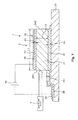
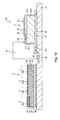
- FIG. 1 is a drawing showing a first embodiment of the terahertz wave generating device of the present invention as taken along a line S-S in FIG. 2 .
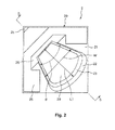
- FIG. 2 is a plan view of the photoconductive antenna of the terahertz wave generating device shown in FIG. 1 .
- FIG. 3 is a cross section perspective view of the light source device of the terahertz wave generating device shown in FIG. 1 .
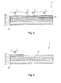
- FIG. 4 is a cross section view as taken along a line A-A in FIG. 3 .
- FIG. 5 is a cross section view as taken along a line B-B in FIG. 3 .
- FIGS. 6A to 6E are plan views showing another constitutional example of the i type semiconductor layer of the photoconductive antenna of the terahertz wave generating device shown in FIG. 1 .
- FIG. 7 is a drawing showing a second embodiment of the terahertz wave generating device of the present invention.
- FIG. 8 is a drawing showing a third embodiment of the terahertz wave generating device of the present invention.
- FIG. 9 is a drawing showing a fourth embodiment of the terahertz wave generating device of the present invention.
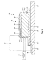
- FIG. 10 is a cross section view showing a fifth embodiment of the terahertz wave generating device of the present invention.
- FIG. 11 is a block diagram showing an embodiment of the imaging device of the present invention.
- FIG. 12 is a plan view showing the terahertz wave detecting unit of the imaging device shown in FIG. 11 .
- FIG. 13 is a graph showing the spectrum in the terahertz band of the object.
- FIG. 14 is a drawing of the image showing the distribution of substances A, B, and C of the object.
- FIG. 15 is a block diagram showing an embodiment of the measuring device of the present invention.
- FIG. 16 is a block diagram showing an embodiment of the camera of the present invention.
- FIG. 17 is a perspective view showing an embodiment of the camera of the present invention.
- FIG. 1 is a drawing showing an embodiment of the terahertz wave generating device of the present invention.
- a cross section view of line S-S in FIG. 2 is shown for the photoconductive antenna, and a block diagram is shown for the light source device.
- FIG. 2 is a plan view of the photoconductive antenna of the terahertz wave generating device shown in FIG. 1 .
- FIG. 3 is a cross section perspective view of the light source device of the terahertz wave generating device shown in FIG. 1 .
- FIG. 4 is a cross section view ofline A-A in FIG. 3 .
- FIG. 5 is a cross section view of line B-B in FIG. 3 .
- FIG. 6 is a plan view showing another constitutional example of the i type semiconductor layer of the photoconductive antenna of the terahertz wave generating device shown in FIG. 1 . Note that hereafter, in FIG. 1 and FIG. 3 to FIG. 5 , the upper side will be described as “upper” and the lower side will be described as “lower.”
- the terahertz wave generating device 1 has a light source device 3 that generates light pulses (pulsed light) which is excitation light, and a photoconductive antenna 2 for generating terahertz waves by irradiating light pulses generated by the light source device 3.
- a terahertz wave means an electromagnetic wave for which the frequency is 100 GHz or greater and 30 THz or less, and particularly an electromagnetic wave of 300 GHz or greater and 3 THz or less.
- the light source device 3 has a light pulse generator 4 that generates light pulses, a first pulse compressor 5 that performs pulse compression on light pulses generated by the light pulse generator 4, a second pulse compressor 7 that performs pulse compression on light pulses for which pulse compression was done by the first pulse compressor 5, and an amplifier 6 that amplifies the light pulses.
- the amplifier 6 can be provided at the front stage of the first pulse compressor 5, or between the first pulse compressor 5 and the second pulse compressor 7, but with the configuration in the drawing, the amplifier 6 is provided between the first pulse compressor 5 and the second pulse compressor 7. With this configuration, the light pulses which underwent pulse compression by the first pulse compressor 5 are amplified by the amplifier 6, and the light pulses amplified by the amplifier 6 undergo pulse compression by the second pulse compressor 7.
- the pulse width (half-value width) of the light pulses emitted from the light source device 3 is not particularly restricted, but is preferably 1 femtosecond or greater and 800 femtoseconds or less, and more preferably 10 femtoseconds or greater and 200 femtoseconds or less.
- the frequency of the light pulses emitted from the light source device 3 is set to the same or greater frequency corresponding to the band gap of the i type semiconductor layer 24 of the photoconductive antenna 2 described later.
- the light pulse generator 4 can use a so-called semiconductor laser such as a DBR laser, DFB laser, mode locked laser or the like, for example.
- the pulse width of the light pulses generated by this light pulse generator 4 is not particularly restricted, but is preferably 1 picosecond or greater and 100 picoseconds or less.
- the first pulse compressor 5 performs pulse compression based on saturable absorption. Specifically, the first pulse compressor 5 has a saturable absorber, and using that saturable absorber, light pulses are compressed and pulse width is decreased.
- the second pulse compressor 7 performs pulse compression based on group velocity dispersion compensation.
- the second pulse compressor 7 has a group velocity dispersion compensation medium, and with this embodiment a coupled waveguide structure, and using that coupled waveguide structure, light pulses are compressed and pulse width is decreased.
- the light pulse generator 4 of the light source device 3, the first pulse compressor 5, the amplifier 6, and the second pulse compressor 7 are made into an integral unit, specifically, integrated on the same substrate.
- the light source device 3 has a substrate 31 which is a semiconductor substrate, a cladding layer 32 which is provided on the substrate 31, an active layer 33 which is provided on the cladding layer 32, a waveguide structure processing etching stop layer 34 provided on the active layer 33, a cladding layer 35 provided on the waveguide structure processing etching stop layer 34, a contact layer 36 provided on the cladding layer 35, an insulation layer 37 provided on the waveguide structure processing etching stop layer 34, a cladding layer 32 side electrode 38 provided on the surface of the substrate 31, and cladding layer 35 side electrodes 391, 392, 393, 394, and 395 provided on the contact layer 36 and the insulation layer 37 surface.
- a diffraction grating 30 is provided between the waveguide structure processing etching stop layer 34 of the light pulse generator 4 and the cladding layer 35.
- the waveguide structure processing etching stop layer is not limited to being provided directly above the active layer, but can also be provided within the cladding layer, for example.
- each part is not particularly restricted, but an example for the substrate 31 and the contact layer 36 is GaAs or the like. Also, an example for the cladding layers 32 and 35, the waveguide structure processing etching stop layer 34, and the diffraction grating 30 includes AlGaAs or the like. Also, for the active layer 33, an example is a structure using a quantum effect called a multiple quantum well or the like. In specific terms, an example of the active layer 33 is an item with a structure called a distributed index of refraction multiple quantum well structured with multiple quantum wells or the like made by alternately providing a plurality of well layers (GaAs well layers) and barrier layers (AlGaAs barrier layers) or the like.
- the waveguide of the light source device 3 is constituted from the cladding layer 32, the active layer 33, the waveguide structure processing etching stop layer 34, and the cladding layer 35.
- the cladding layer 35 is provided in a shape corresponding to the waveguide, only on the top part of the waveguide.
- the cladding layer 35 is formed by removal of the unnecessary parts by etching. Depending on the manufacturing method, it is possible to omit the waveguide structure processing etching stop layer 34.
- two each of the cladding layer 35 and the contact layer 36 are provided.
- One of the cladding layer 35 and the contact layer 36 constitute the light pulse generator 4, the first pulse compressor 5, the amplifier 6, and part of the second pulse compressor 7, and are provided sequentially, and the other cladding layer 35 and contact layer 36 constitute part of the second pulse compressor 7.
- one pair of cladding layers 35 and one pair of contact layers 36 are provided on the second pulse compressor 7.
- the electrode 391 is provided so as to correspond to the cladding layer 35 of the light pulse generator 4
- the electrode 392 is provided so as to correspond to the cladding layer 35 of the first pulse compressor 5
- the electrode 393 is provided so as to correspond to the cladding layer 35 of the amplifier 6,
- the electrodes 394 and 395 are provided so as to respectively correspond to the two cladding layers 35 of the second pulse compressor 7.
- the electrode 38 is a shared electrode of the light pulse generator 4, the first pulse compressor 5, the amplifier 6, and the second pulse compressor 7.
- the pair of electrodes of the light pulse generator 4 is constituted by the electrode 38 and the electrode 391
- the pair of electrodes of the first pulse compressor 5 is constituted by the electrode 38 and the electrode 392
- the pair of electrodes of the amplifier 6 is constituted by the electrode 38 and the electrode 393
- the two pairs of electrodes of the second pulse compressor 7 are constituted by the electrode 38 and electrode 394 and the electrode 38 and electrode 395.
- the overall shape of the light source device 3 is a rectangular solid with the constitution in the drawing, but naturally it is not restricted to this.
- the dimensions of the light source device 3 are not particularly restricted, but for example can be 1 mm or greater and 10 mm or less x 0.5 mm or greater and 5 mm or less x 0.1 mm or greater and 1 mm or less.
- the constitution of the light source device is not restricted to the previously described constitution.
- the photoconductive antenna 2 has a substrate 21 and a photoconductive antenna main unit 20 provided on the substrate 21.
- the substrate 21 is not restricted provided it is an item that can support the photoconductive antenna main unit 20, and though it is possible to use a semiconductor substrate constituted by various types of semiconductor material, a resin substrate constituted by various types of resin material, or a glass substrate constituted by various types of glass material, a semiconductor substrate is preferable. Also, when using a semiconductor substrate as the substrate 21, as its semiconductor material, though not particularly restricted, it is possible to use various types of items, but a III-V compound semiconductor is preferable. Also, as the III-V compound semiconductor, though not particularly restricted, examples include GaAs, InP, InAs, InSb and the like.
- the shape of the substrate 21 is rectangular when seen from the lamination direction (as viewed along the lamination direction) of the n type semiconductor layer 22, the i type semiconductor layer 24, and the p type semiconductor layer 23 described later.
- the shape of the substrate 21 is not restricted to being rectangular, and can also be a circle, an oval, or another polygon or the like such as a triangle, a pentagon, a hexagon or the like.
- the lamination direction of the n type semiconductor layer 22, the i type semiconductor layer 24, and the p type semiconductor layer 23 is also called “the planar view.” Also, “the lamination direction of the n type semiconductor layer 22, the i type semiconductor layer 24, and the p type semiconductor layer 23" is also simply stated as “the lamination direction.”
- the photoconductive antenna main unit 20 has an n type semiconductor layer (first conductive layer) 22, an i type semiconductor layer (semiconductor layer) 24 that generates terahertz waves and has the function of leading those terahertz waves, a p type semiconductor layer (second conductive layer) 23, an insulation layer 25, and an electrode (first electrode) 28 and an electrode (second electrode) 29 constituting the pair of electrodes.
- the n type semiconductor layer 22, the i type semiconductor layer 24, and the p type semiconductor layer 23 are laminated (provided) in that order from the substrate 21 side.
- a laminated body (pin structure) for which the n type semiconductor layer 22, the i type semiconductor layer 24, and the p type semiconductor layer 23 are laminated in that order from the substrate 21 side.
- the i type semiconductor layer 24 is formed sandwiched by the n type semiconductor layer 22 and the p type semiconductor layer 23.
- the side surface of the left side in FIG. 1 constitutes the incidence surface 241 at which the light pulses are made incident
- the end surface of the right side in FIG. 1 constitutes the emission surface 242 at which the terahertz waves generated by the i type semiconductor layer 24 are emitted.
- the light pulses are made incident on the i type semiconductor layer 24 directly, without passing through the n type semiconductor layer 22 or the p type semiconductor layer 23, so it is possible to prevent the absorption of the light pulses by the n type semiconductor layer 22 or the p type semiconductor layer 23, making it possible to generate terahertz waves with good efficiency.
- the insulation layer 25 is provided on the substrate 21, and at a site at which the i type semiconductor layer 24 is not provided on the n type semiconductor layer 22. Also, an aperture 251 is formed on a portion of the insulation layer 25 on the n type semiconductor layer 25.
- the electrode 28 is provided on the insulation layer 25, and is in contact with the n type semiconductor layer 22 via the aperture 251, and is electrically connected to that n type semiconductor layer 22.
- the electrode 29 is provided on the p type semiconductor layer 23. Specifically, the electrode 29 is in contact with the p type semiconductor layer 23, and is electrically connected to that p type semiconductor layer 23. This electrode 29 is provided on roughly the entire p type semiconductor layer 23, and also works as a reflective layer for reflecting the terahertz waves generated by the i type semiconductor layer 24. With this configuration, it is possible to reflect the terahertz waves that leak to the outside from the top surface of the p type semiconductor layer 23 to the i type semiconductor layer 24 side (to the side of the laminated body interior), making it possible to lead terahertz waves efficiently.
- the shape of the i type semiconductor layer 24 is not particularly restricted, but it is preferably an elongated shape.
- an elongated shape indicates a shape for which with a planar view, compared to the length of one direction, the length of the other direction orthogonal to that one direction is longer. Then, if this condition is fulfilled, the shape is not restricted to being a rectangle.
- the i type semiconductor layer 24 has an elongated shape, in specific terms, with the planar view, has a shape for which the center side part of a fan shape (the part including the intersection of the two straight lines constituting the outer form of the fan shape) is removed.
- the incidence surface 241 of the i type semiconductor layer 24 is a flat plane
- the emission surface 242 is a curved convex surface (curved surface).
- the shape of the incidence surface 241 of the i type semiconductor layer 24 is a straight line shape
- the shape of the emission surface 242 is an arc shape (curved line shape).
- the width W of the i type semiconductor layer 24 gradually increases from the incidence surface 241 side toward the emission surface 242 side.
- the length L1 of the lengthwise direction orthogonal to the width W of the i type semiconductor layer 24 is larger than the maximum width W of the i type semiconductor layer 24.
- the i type semiconductor layer 24 may also have the width W for only a portion thereof gradually increase from the incidence surface 241 side toward the emission surface 242 side. Specifically, with a planar view, the i type semiconductor layer 24 may also have a site for which the width W gradually increases from the incidence surface 241 side toward the emission surface 242 side.
- the dimensions of the i type semiconductor layer 24 are not particularly restricted, and are set as appropriate according to various conditions, but the length L1 of the lengthwise direction of the i type semiconductor layer 24 is preferably 30 ⁇ m or greater and 3 mm or less, and more preferably 30 ⁇ m or greater and 0.3 mm or less. Also, the angle (center angle) ⁇ in the drawing of the i type semiconductor layer 24 is preferably 5° or greater and 170° or less, and more preferably 10° or greater and 90° or less.
- the shapes of the n type semiconductor layer 22 and the p type semiconductor 23 are not particularly restricted, but with the configuration in the drawing, with a planar view, the n type semiconductor layer 22 is formed so as to contain the i type semiconductor layer 24 and the p type semiconductor layer 23. Also, the i type semiconductor layer 24 and the p type semiconductor layer 23 have the same shape with the planar view. In this way, with the planar view, the n type semiconductor layer 22 and the p type semiconductor layer 23 are formed so as to have the same shape as the i type semiconductor layer 24 or to contain the i type semiconductor layer 24, and with this configuration, with the planar view, terahertz waves are generated on roughly the entire i type semiconductor layer 24, so it is possible to generate high intensity terahertz waves.
- the n type semiconductor layer 22 is constituted from a semiconductor material containing an n type (first conductive type) impurity.
- the carrier density (impurity concentration) of the n type semiconductor layer 22 is preferably 1 x 10 17 /cm 3 or greater, more preferably 1 x 10 20 /cm 3 or greater, and even more preferably 1 x 10 20 /cm 3 or greater and 1 x 10 25 /cm 3 or less.
- the n type impurity is not particularly restricted, but examples include Si, Ge, S, Se or the like.
- the thickness d1 of the n type semiconductor layer 22 is not particularly restricted, and is set as appropriate according to various conditions, but is preferably 1 ⁇ m or greater and 4 mm or less, and more preferably 1 ⁇ m or greater and 10 ⁇ m or less.
- the p type semiconductor layer 23 is constituted by a semiconductor material containing a p type (second conductive type) impurity.
- the carrier density of the p type semiconductor layer 23 is preferably 1 x 10 17 /cm 3 or greater, more preferably 1 x 10 20 /cm 3 or greater, and even more preferably 1 x 10 20 /cm 3 or greater and 1 x 10 25 /cm 3 or less.
- This p type impurity is not particularly restricted, but examples include Zn, Mg, C or the like.
- the thickness d2 of the p type semiconductor layer 23 is not particularly restricted, and is set as appropriate according to various conditions, but is preferably 1 ⁇ m or greater and 2 mm or less, and more preferably 1 ⁇ m or greater and 10 ⁇ m or less.
- the i type semiconductor layer 24 is constituted with a semiconductor material.
- the semiconductor material constituting this i type semiconductor layer 24 is preferably an intrinsic semiconductor, but may also include a small volume of an n type impurity or a p type impurity.
- the i type semiconductor layer 24 can be said to have a carrier density lower than an n type semiconductor 22 when it contains an n type impurity, and can be said to have a carrier density lower than a p type semiconductor when it contains a p type impurity. It is preferable that even when the i type semiconductor layer 24 contains either the n type impurity or the p type impurity, the carrier density is lower than with the n type semiconductor layer 22 and the p type semiconductor layer 23.
- the carrier density of the i type semiconductor layer 24 is preferably 1 x 10 18 cm 3 or less, more preferably 1 x 10 12 /cm 3 or greater and 1 x 10 18 /cm 3 or less, and even more preferably 1 x 10 12 /cm 3 or greater and 1 x 10 16 /cm 3 or less.
- the thickness d3 of the i type semiconductor layer 24 is not particularly restricted, and is set as appropriate according to various conditions, but is preferably 1 ⁇ m or greater and 4 mm or less, and more preferably 1 ⁇ m or greater and 10 ⁇ m or less.
- the thickness d3 of the i type semiconductor layer 24 is less than the lower limit value noted above, forming of the i type semiconductor layer 24 may be difficult depending on other conditions, and if it exceeds the upper limit value noted above, the withstand voltage may be insufficient depending on other conditions, so it is not possible to form an electric field of a large field intensity inside the i type semiconductor layer 24, and because of that, it is not possible to generate high intensity terahertz waves.
- the semiconductor material of the p type semiconductor layer 23, the n type semiconductor layer 33, and the i type semiconductor layer 24 is not particularly restricted, and it is possible to use various types of items, but it is preferable to use a III-V compound semiconductor.
- the III-V compound semiconductor is not particularly restricted, and examples include GaAs, InP, InAs, InSb and the like.
- the material of the insulation layer 25 is not particularly restricted as long as it is a material having insulating properties, and examples include fluorine based resin, polyimide, a borazine compound, hydrogenated siloxane, benzocyclobutene, SiN, SiO 2 and the like.
- a power supply device 18 is electrically connected to the electrodes 28 and 29 respectively via a pad, conducting wire, connector or the like (not illustrated), and direct current voltage is applied between the electrode 28 and the electrode 29 so that the electrode 28 side is positive.
- the terahertz wave generating device 1 With the terahertz wave generating device 1, first, light pulses are generated by the light pulse generator 4 of the light source device 3.
- the pulse width of the light pulses generated by the light pulse generator 4 is larger than the target pulse width.
- the light pulses generated by the light pulse generator 4 pass through the waveguide, and pass through the first pulse compressor 5, the amplifier 6, and the second pulse compressor 7 sequentially in that order.
- pulse compression based on saturable absorption is performed on the light pulses, and the pulse width of the light pulses is decreased.
- the amplifier 6 the light pulses are amplified.
- pulse compression based on group velocity dispersion compensation is performed on the light pulses, and the pulse width of the light pulses is decreased. In this way, light pulses of the target pulse width are generated, and are emitted from the second pulse compressor 7.
- the light pulses emitted from the light source device 3 are irradiated at the incidence surface 241 of the i type semiconductor layer 24 from the side of the photoconductive antenna 2, are made incident from the incidence surface 241 into the i type semiconductor layer 24, and terahertz waves are generated at the i type semiconductor layer 24.
- These terahertz waves are lead by the i type semiconductor layer 24, and advance within that i type semiconductor layer 24 toward the emission surface 242 side.
- the terahertz waves that advance inside the i type semiconductor layer 24 the terahertz waves that pass through the p type semiconductor layer 23 are reflected by the electrode 29, and are prevented from leaking from the top surface of the p type semiconductor layer 23, and this makes it possible for the terahertz waves to be led efficiently.
- terahertz waves having directionality in the lengthwise direction of the i type semiconductor layer 24 are emitted from the emission surface 242.
- the light pulses are made incident on the i type semiconductor layer 24 directly without going via the n type semiconductor layer 22 or the p type semiconductor 23, so it is possible to prevent the light pulses from being partially absorbed by the n type semiconductor layer 22 or the p type semiconductor layer 23, making it possible to generate terahertz waves efficiently.
- the terahertz waves generated by the i type semiconductor layer 24 are led in a designated direction by that i type semiconductor layer 24, and with this configuration, it is possible to generate terahertz waves having directionality.
- the light source device 3 has the first pulse compressor 5, the amplifier 6, and the second pulse compressor 7, so it is possible to make the light source device 3 more compact, and thus the terahertz wave generating device 1 more compact, and it is also possible to generate light pulses with a desired wave height and desired width, and with this configuration, it is possible to reliably generate the desired terahertz waves.
- the shape of the i type semiconductor layer 24 of the photoconductive antenna 2 is not restricted to the item described above, and other examples include the items such as those shown in FIG. 6A to FIG. 6E .
- the incidence surface 241 of the i type semiconductor layer 24 is a curved concave surface (curved surface), and the emission surface 242 is a curved convex surface (curved surface).
- the i type semiconductor layer 24 incidence surface 241 shape and the emission surface 242 shape are respectively arc shapes (curved line shapes).
- the curvature radius of the incidence surface 241 and the curvature radius of the emission surface 242 may be the same, or may be different.
- the i type semiconductor layer 24 incidence surface 241 and emission surface 242 are respectively curved convex surfaces (curved surfaces).
- the i type semiconductor layer 24 incidence surface 241 shape and the emission surface 242 shape are respectively arc shapes (curved line shapes).
- the curvature radius of the incidence surface 241 and the curvature radius of the emission surface 242 may be the same, or may be different.
- the i type semiconductor, layer 24 incidence surface 241 and emission surface 242 are respectively flat planes.
- the i type semiconductor layer 24 incidence surface 241 shape and the emission surface 242 shape are straight lines.
- the i type semiconductor layer 24 can also be called a trapezoid.
- the i type semiconductor layer 24 incidence surface 241 is a curved concave surface (curved surface), and the emission surface 242 is a flat plane.
- the i type semiconductor layer 24 incidence surface 241 shape is an arc shape (curved line shape), and the emission surface 242 shape is a straight line shape.
- the i type semiconductor layer 24 incidence surface 241 is a curved convex surface (curved surface), and the emission surface 242 is a flat plane.
- the i type semiconductor layer 24 incidence surface 241 shape is an arc shape (curved line shape), and the emission surface 242 shape is a straight line shape.
- a terahertz wave generating device 1A in accordance with a second embodiment will now be explained.
- the parts of the second embodiment that are identical to the parts of the first embodiment will be given the same reference numerals as the parts of the first embodiment.
- the descriptions of the parts of the second embodiment that are identical to the parts of the first embodiment may be omitted for the sake of brevity.
- FIG. 7 is a drawing showing the terahertz wave generating device 1A according to the second embodiment of the present invention.
- a cross section diagram is shown for the photoconductive antenna, and a block diagram is shown for the light source device.
- the upper side will be described as “upper” and the lower side will be described as “lower.”
- a p type semiconductor layer 23' of the photoconductive antenna 2 is provided only on a portion of the incidence surface 241 side on the i type semiconductor layer 24.
- the incidence surface 241 of the i type semiconductor layer 24 is flush with the end surface of the incidence surface side of the p type semiconductor layer 23' (the side surface, specifically, the surface having a normal line perpendicular to the lamination direction), and the length of the p type semiconductor layer 23' (length in the same direction as L1) L2 is set to be shorter than the length L1 of the lengthwise direction of the i type semiconductor layer 24.
- terahertz waves are generated only on a portion of the incidence surface 241 side of the i type semiconductor layer 24, so it is possible to suppress interference between terahertz waves generated in the plurality of regions within the i type semiconductor layer 24.
- the dimensions of the p type semiconductor layer 23' are not particularly restricted as long as they are smaller than those of the i type semiconductor layer 24, and are set as appropriate according to various conditions, but the length L2 of the p type semiconductor layer 23' is preferably 1 ⁇ m or greater and 2 mm or less, and more preferably 3 ⁇ m or greater and 30 ⁇ m or less. Also, L2/L1 is preferably 0.00033 or greater and 0.667 or less, and more preferably 0.001 or greater and 0.1 or less.
- an insulation layer 26 is provided continuously with the p type semiconductor layer 23'.
- the material of this insulation layer 26 is not particularly restricted as long as it is a material having insulating properties, and for example it is possible to use the same material as the previously described insulation layer 25.
- a terahertz wave generating device 1B in accordance with a third embodiment will now be explained.
- the parts of the third embodiment that are identical to the parts of the first or second embodiment will be given the same reference numerals as the parts of the first or second embodiment.
- the descriptions of the parts of the third embodiment that are identical to the parts of the first or second embodiment may be omitted for the sake of brevity.
- FIG. 8 is a drawing showing the terahertz wave generating device 1B according to the third embodiment of the present invention.
- a cross section diagram is shown for the photoconductive antenna, and a block diagram is shown for the light source device.
- the upper side will be described as “upper” and the lower side will be described as “lower.”
- the photoconductive antenna 2 has a covering layer 27.
- This covering layer 27 covers the part of the i type semiconductor layer 24 at the side surface of the laminated body, specifically, the surface of the i type semiconductor layer 24 having a normal line perpendicular to the lamination direction.
- the covering layer 27 covers the entire surface that is exposed between the i type semiconductor layer 24 n type semiconductor layer 22 and the p type semiconductor layer 23'. With this configuration, the i type semiconductor layer 24 is sealed, making it possible to prevent corrosion or the like of the i type semiconductor layer 24.
- the thickness d4 of the covering layer 27 is not particularly restricted, and is set as appropriate according to various conditions, but it is preferably 10 nm or greater and 1 mm or less, more preferably 1 ⁇ m or greater and 100 ⁇ m or less, and in particular, the thickness d4 of the covering layer 27 provided on the incidence surface 241 of the i type semiconductor layer 24 is preferably 1 nm or greater and 100 ⁇ m or less, and more preferably 10 nm or greater and 1 ⁇ m or less.
- the material of the covering layer 27 is not particularly restricted as long as it is a material that can seal the i type semiconductor layer 24, but it is preferable that the relative dielectric constant (dielectric constant) of the material of the covering layer 27 is lower than the relative dielectric constant of the semiconductor material constituting the i type semiconductor layer 24.
- the terahertz waves have the physical property of trying to advance in a material with a higher dielectric constant, so with this configuration, it is possible for the terahertz waves to be led efficiently by the i type semiconductor layer 24.
- the relative dielectric constant of the material of the covering layer 27 is 20 or less, and more preferably 2 or greater and 10 or less.
- covering layer 27 material examples include polyimide (relative dielectric constant: 3), a borazine compound (relative dielectric constant: 2.3), SiN (relative dielectric constant: 7), SiO 2 (relative dielectric constant: 4), hydrogenated siloxane (relative dielectric constant: 3), benzocyclobutene (relative dielectric constant: 2.7), fluorine based resin (relative dielectric constant: 2.7) and the like.
- the structures of the covering layer 27 in the third embodiment can also be applied to the first embodiment.
- a terahertz wave generating device 1C in accordance with a fourth embodiment will now be explained.
- the parts of the fourth embodiment that are identical to the parts of the first, second or third embodiment will be given the same reference numerals as the parts of the first, second or third embodiment.
- the descriptions of the parts of the fourth embodiment that are identical to the parts of the first, second or third embodiment may be omitted for the sake of brevity.
- FIG. 9 is a drawing showing the terahertz wave generating device 1C according to the fourth embodiment of the present invention.
- a cross section diagram is shown for the photoconductive antenna, and a block diagram is shown for the light source device.
- the upper side will be described as “upper” and the lower side will be described as “lower.”
- the relative dielectric constant (dielectric constant) of a material of a covering layer 27a provided on the emission surface 242 of the i type semiconductor layer 24 is higher than the relative dielectric constant of the semiconductor material constituting the i type semiconductor layer 24.
- the terahertz waves have a physical property of trying to advance in the substance with the higher dielectric constant, so it is possible to reliably emit terahertz waves generated by the i type semiconductor layer 24 from the emission surface 242 of that i type semiconductor layer 24, making it possible to generate high intensity terahertz waves.
- the thickness d5 of the covering layer 27a is not particularly restricted, and is set as appropriate according to various conditions, but it is preferably 10 nm or greater and 1 mm or less, and more preferably 1 ⁇ m or greater and 100 ⁇ m or less.
- the material of the covering layer 27a is not particularly restricted as long as its relative dielectric constant is higher than the relative dielectric constant of the semiconductor material constituting the i type semiconductor layer 24, specifically, is a dielectric material, but the relative dielectric constant of the dielectric material constituting the covering layer 27a is preferably 20 or greater, and more preferably 30 or greater and 200 or less.
- examples include nitrogen-added hafnium aluminate (relative dielectric constant: 20), hafnium oxide (relative dielectric constant: 23), yttrium oxide (relative dielectric constant: 25), lanthanum oxide (relative dielectric constant: 27), niobium pentoxide (relative dielectric constant: 41), titanium dioxide (rutile) (relative dielectric constant: 80), and titanium oxide (relative dielectric constant: 160) and the like.
- the covering layer 27 other than the covering layer 27a is the same as that of the previously described third embodiment, so a description of that is omitted.
- the structure of the covering layer 27a in the fourth embodiment can also be applied to the first or second embodiment.
- a terahertz wave generating device 1D in accordance with a fifth embodiment will now be explained.
- the parts of the fifth embodiment that are identical to the parts of the first, second, third or fourth embodiment will be given the same reference numerals as the parts of the first, second, third or fourth embodiment.
- the descriptions of the parts of the fifth embodiment that are identical to the parts of the first, second or third embodiment may be omitted for the sake of brevity.
- FIG. 10 is a cross section diagram showing the terahertz wave generating device 1D according to the fifth embodiment of the present invention.
- the upper side will be described as “upper” and the lower side will be described as “lower.”
- the light source device 3 and the photoconductive antenna 2 are respectively provided on the substrate 21.
- This light source device 3 and the photoconductive antenna 2 are respectively formed on the substrate 21 and formed as an integral unit with the substrate 21.
- the light source device 3 and the photoconductive antenna 2 are given a monolithic structure.
- the alignment of the light source device 3 and the photoconductive antenna 2 can be performed at the same time as when the light source device 3 and the photoconductive antenna 2 are formed on the substrate 21, so it is possible to perform higher precision alignment within the process range of error. Because of that, compared to when the light source device 3 and the photoconductive antenna 2 are manufactured separately, and they are installed on abase while aligning them, it is possible to more easily manufacture the terahertz wave generating device 1.
- the light source device 3 and the photoconductive antenna 2 are given a monolithic structure, so it is possible to make the terahertz wave generating device more compact.
- the structure of the photoconductive antenna in the terahertz wave generation device 1D is basically the same as the structure of the photoconductive antenna in the terahertz wave generation device 1C in the fourth embodiment. It will be apparent to those skilled in the art from this disclosure that the structure of the photoconductive antenna in the terahertz wave generation device 1, 1A or 1B in the first, second or third embodiment can also be applied to the terahertz wave generation device 1D of the fifth embodiment.
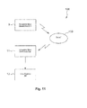
- FIG. 11 is a block diagram showing an embodiment of the imaging device of the present invention.
- FIG. 12 is a plan view showing the terahertz wave detecting unit of the imaging device shown in FIG. 11 .
- FIG. 13 is a graph showing the spectrum of the terahertz band of the object.
- FIG. 14 is a drawing of an image showing the distribution of the substances A, B, and C of the object.
- the imagine device 100 is equipped with a terahertz wave generating unit 9, a terahertz wave detecting unit 11 for detecting terahertz waves emitted from the terahertz wave generating unit 9 and passed through or reflected by the object 150, and an image forming unit 12 that generates an image of the object 150. specifically, image data, based on the detection results of the terahertz wave detecting unit 11.
- the configuration of the terahertz wave generating unit 9 is the same as the previously noted terahertz wave generating device 1, so a description will be omitted here.
- any of the terahertz wave generating devices 1, 1A, 1B, 1C and 1D described in the first through fifth embodiment can be used as the terahertz wave generating unit 9.
- the terahertz wave detecting unit 11 an item is used that is equipped with a filter 15 that transmits terahertz waves of target wavelengths, and a detection unit 17 that detects the terahertz waves of the target wavelengths transmitted by the filter 15.
- the detection unit 17 for example, an item is used that converts terahertz waves to heat and detects it, specifically, an item that converts terahertz waves to heat, and detects the energy (intensity) of the terahertz waves.
- examples include pyroelectric sensors, bolomoters and the like.
- the terahertz wave detecting unit 11 is not restricted to an item of this constitution.
- the filter 15 has a plurality of pixels (unit filter units) 16 arranged two dimensionally. Specifically, the pixels 16 are arranged in matrix form.
- each pixel 16 has a plurality of fields that transmit terahertz waves of mutually different wavelengths, specifically, a plurality of fields that have mutually different transmitted terahertz wavelengths (hereafter also called "transmission wavelengths").
- transmission wavelengths a plurality of fields that have mutually different transmitted terahertz wavelengths.
- the detection unit 17 has a first unit detecting unit 171, a second unit detecting unit 172, a third unit detecting unit 173, and a fourth unit detecting unit 174 provided respectively corresponding to the first field 161, second field 162, third field 163, and fourth field 164 of each pixel 16 of the filter 15.
- Each first unit detecting unit 171, second unit detecting unit 172, third unit detecting unit 173, and fourth unit detecting unit 174 respectively convert to heat and detect terahertz waves that were transmitted through the first field 161, the second field 162, the third field 163, and the fourth field 164 of each pixel 16.
- the object 150 that is the subject of spectral imaging is constituted by three substances A, B, and C.
- the imaging device 100 performs spectral imaging of this object 150.
- the terahertz wave detecting unit 11 detects terahertz waves reflected by the object 150.
- a first field 161 and a second field 162 are used.
- the transmission wavelength ⁇ 1 of the first field 161 and the transmission wavelength ⁇ 2 of the second field 162 are set so that the difference ( ⁇ 2 - ⁇ 1) between the intensity ⁇ 2 and intensity ⁇ 1 can be clearly mutually distinguished for the substance A, substance B, and substance C.
- the difference between the intensity ⁇ 2 of they wavelength ⁇ 2 component of the terahertz waves reflected by the object 150 and the intensity ⁇ 1 of the wavelength ⁇ 1 component ( ⁇ 2 - ⁇ 1) is a positive value.
- the imaging device 100 when performing spectral imaging of the object 150, first, terahertz waves are generated by the terahertz wave generating unit 9, and those terahertz waves are irradiated on the object 150. Then, the terahertz wave detecting unit 11 detects the terahertz waves reflected by the object 150 as ⁇ 1 and ⁇ 2. These detection results are sent to the image forming unit 12. The detection of irradiation of terahertz waves on the object 150 and terahertz waves reflected by the object 150 is performed for the overall object 150.
- the image forming unit 12 finds the difference ( ⁇ 2 - ⁇ 1) between the intensity ⁇ 2 of the wavelength ⁇ 2 component of the terahertz waves transmitted through the second field 162 of the filter 15 and the intensity ⁇ 1 of the wavelength ⁇ 1 component of the terahertz waves transmitted through the first field 161 based on the detection results. Then, of the object 150, sites for which the difference is a positive value are determined and specified as being substance A, sites for which the difference is zero as substance B, and sites for which the difference is a negative value as substance C.
- the image forming unit 12 creates image data of an image showing the distribution of the substances A, B and C of the object 150.
- This image data is sent to a monitor (not illustrated) from the image forming unit 12, and an image showing the distribution of the substance A, substance B, and substance C of the object 150 is displayed on the monitor.
- a monitor not illustrated
- color coded display is done so that the field in which substance A of the object 150 is distributed is shown as black, the field in which substance B is distributed is shown as gray, and the field in which substance C is distributed is shown as white.
- the application of the imaging device 100 is not limited to the item described above, and for example, it is possible to irradiate terahertz waves on a person, to detect terahertz waves transmitted or reflected by that person, and by performing processing at the image forming unit 12, it is possible to determine whether that person is holding a gun, knife, illegal drugs or the like.
- FIG. 15 is a block diagram showing an embodiment of the measuring device of the present invention.
- the measuring device 200 is equipped with a terahertz wave generating unit 9 for generating terahertz waves, a terahertz wave detecting unit 11 for detecting terahertz waves emitted from the terahertz wave generating unit 9 and transmitted through or reflected by the object 160, and a measuring unit 13 for measuring the obj ect 160 based on the detection results of the terahertz wave detecting unit 11.
- the measuring device 200 when performing spectroscopic measurement of the object 160, first, terahertz waves are generated by the terahertz wave generating unit 9, and those terahertz waves are irradiated on the object 160. Then, the terahertz waves transmitted by or reflected by the object 160 are detected by the terahertz wave detecting unit 11. These detection results are sent to the measuring unit 13. Irradiation of the terahertz waves on the object 160 and detection of the terahertz waves transmitted by or reflected by the object 160 are performed for the overall object 160.
- the measuring unit 13 From the detection results, the respective intensities of the terahertz waves that were transmitted through the first field 161, the second field 162, the third field 163, and the fourth field 164 of the filter 15 are found out, and analysis or the like of the object 160 components and their distribution is performed.
- FIG. 16 is a block diagram showing the embodiment of the camera of the present invention. Also, FIG. 17 shows a schematic perspective view showing an embodiment of the camera of the present invention.
- the camera 300 is equipped with a terahertz waive generating unit 9 for generating terahertz waves, a terahertz wave detecting unit 11 for detecting terahertz waves emitted from the terahertz wave generating unit 9 and reflected by the object 170, and a memory unit 14. Then, each of these parts is housed in a case 310 of the camera 300.
- the camera 300 is equipped with a lens (optical system) 320 for converging (imaging) the terahertz waves reflected by the object 170 on the terahertz wave detecting unit 11, and a window part 330 for emitting to outside the case 310 the terahertz waves generated by the terahertz wave generating unit 9.
- the lens 320 and the window part 330 are constituted by members using silicon, quartz, polyethylene or the like that transmit or refract terahertz waves.
- the window part 330 can also be constituted with an aperture simply provided as a slit.
- terahertz waves are generated by the terahertz wave generating unit 9, and those terahertz waves are irradiated on the object 170. Then, the terahertz waves reflected by the object 170 are converged (imaged) by the lens 320 to the terahertz wave detecting unit 11 and detected.
- the detection results are sent to and stored in the memory unit 14. Detection of irradiation of the terahertz waves on the object 170 and of the terahertz waves reflected by the object 170 is performed on the overall object 170.
- the detection results can also be sent to an external device such as a personal computer or the like, for example. With the personal computer, it is possible to perform various processes based on the detection results.
- the photoconductive antenna, the terahertz wave generating device, the camera, the imaging device, and the measuring device of the present invention were described based on the embodiments in the drawings, but the present invention is not limited to this, and the constitution of each part can be replaced with an item of any constitution having the same functions. It is also possible to add any other constituent materials to the present invention.
- an n type semiconductor layer was used as the first conductive layer
- a p type semiconductor layer was used as the second conductive layer
- the light pulse generator can be a separate item from the light source device.
Landscapes
- Physics & Mathematics (AREA)
- Electromagnetism (AREA)
- Optics & Photonics (AREA)
- Investigating Or Analysing Materials By Optical Means (AREA)
- Light Receiving Elements (AREA)
Abstract
Description
- This application claims priority to Japanese Patent Application No.
2011-290068 filed on December 28, 2011 2011-290068 - The present invention relates to a photoconductive antenna, a terahertz wave generating device, a camera, an imaging device, and a measuring device.
- In recent years, attention has been devoted to terahertz waves, which are electromagnetic waves with frequencies of 100 GHz or greater and 30 THz or less. Terahertz waves can be used in various forms of measurement and non-destructive testing such as imaging and spectrometry.
- The terahertz wave generating device that generates these terahertz waves has a light source device that generates light pulses (pulsed light) having pulse widths at the approximately sub picosecond level (several hundred femtoseconds) and a photoconductive antenna that generates terahertz waves by irradiating light pulses generated by the light pulse generator.
- As the photoconductive antenna, for example, disclosed in Japanese Laid-Open Patent Application Publication No.
2007-300022 - With the photoconductive antenna noted in the above mentioned publication, for a dipole shaped photoconductive antenna (PCA) using a low temperature growth GaAs (LT-GaAs) substrate, it is possible to make the intensity of the generated terahertz waves approximately 10 times larger.
- However, with the photoconductive antenna noted in the above mentioned publication, light pulses are irradiated on the p type semiconductor layer, and the light pulses that pass through that p type semiconductor layer are made incident on the i type semiconductor layer, so a portion of the light pulses are absorbed by the p type semiconductor layer, and because of that, there is the problem that the terahertz wave generating efficiency decreases.
- An object of the present invention is to provide a photoconductive antenna, a terahertz wave generating device, a camera, an imaging device, and a measuring device capable of generating terahertz waves with better efficiency than the prior art.
- This kind of object is achieved by the present invention noted hereafter.
- A photoconductive antenna according to one aspect of the present invention is adapted to generate terahertz waves when irradiated by pulsed light. The photoconductive antenna includes a first conductive layer, a second conductive layer, a semiconductor layer, a first electrode and a second electrode. The first conductive layer is made of a semiconductor material containing a first conductive type impurity. The second conductive layer is made of a semiconductor material containing a second conductive type impurity different from the first conductive type impurity. The semiconductor layer is positioned between the first conductive layer and the second conductive layer, and made of a semiconductor material having a carrier density that is lower than a carrier density of the semiconductor material of the first conductive layer or a carrier density of the semiconductor material of the second conductive layer. The first electrode is electrically connected to the first conductive layer. The second electrode is electrically connected to the second conductive layer. The semiconductor layer includes an incidence surface through which the pulsed light enters the semiconductor layer, and an emission surface from which the terahertz waves are emitted. The incidence surface is positioned in a side surface of the semiconductor layer having a normal direction extending orthogonal to a lamination direction of the first conductive layer, the semiconductor layer, and the second conductive layer, and the emission surface is positioned in the side surface of the semiconductor layer at a position different from the incidence surface.
- With this configuration, the light pulses (pulsed light) are made incident to the semiconductor directly without going via the semiconductor layer containing a first impurity or the semiconductor layer containing a second impurity, so it is possible to prevent absorption of the light pulses by the semiconductor layer containing a first impurity or the semiconductor layer containing a second impurity, making it possible to generate terahertz waves efficiently.
- Also, it is possible to manufacture the terahertz wave generating device by forming the photoconductive antenna and the light source for generating light pulses on a substrate as an integrated unit with that substrate, and with this configuration, it is possible to make the terahertz wave generating device more compact. Also, it is possible to perform alignment of the light source and the photoconductive antenna when forming that light source and photoconductive antenna on the substrate, and with this configuration, it is possible to manufacture the terahertz wave generating device easily.
- With the photoconductive antenna according to the above described aspect of the present invention, the semiconductor layer preferably has an elongated shape in which a direction from the incidence surface toward the emission surface is a lengthwise direction as viewed along the lamination direction.
- With this configuration, using the semiconductor layer, it is possible to lead the terahertz waves along the lengthwise direction of that semiconductor layer. Therefore, it is possible to generate terahertz waves with directionality.
- With the photoconductive antenna according to the above described aspect of the present invention, a width of a part of the semiconductor layer as viewed along the lamination direction preferably increases in a direction from the incidence surface toward the emission surface, the width being defined in a direction orthogonal to the direction from the incidence surface toward the emission surface.
- With this configuration, it is possible for terahertz waves to be led efficiently by the semiconductor layer.
- With the photoconductive antenna according to the above described aspect of the present invention, the second conductive layer is preferably provided only on a portion of the semiconductor layer, and a side surface of the second conductive layer having a normal direction extending orthogonal to the lamination direction is flush with the incidence surface of the semiconductor layer.
- With this configuration, terahertz waves are generated only on a portion of the incidence surface side of the semiconductor layer, so it is possible to suppress interference between terahertz waves within the semiconductor layer.
- The photoconductive antenna according to the above described aspect of the present invention preferably further includes a covering layer covering the side surface of the semiconductor layer.
- With this configuration, it is possible to prevent corrosion of the semiconductor layer.
- With the photoconductive antenna according to the above described aspect of the present invention, a relative dielectric constant of a material of the covering layer provided on the emission surface is preferably higher than a relative dielectric constant of the semiconductor material of the semiconductor layer.
- The terahertz waves have the physical property of trying to advance in a material with a higher dielectric constant. Therefore, it is possible to reliably emit terahertz waves generated by the semiconductor layer from the emission surface of that semiconductor layer.
- With the photoconductive antenna according to the above described aspect of the present invention, the semiconductor material of the semiconductor layer is preferably a III-V compound.
- With this configuration, it is possible to generate high intensity terahertz waves.
- A terahertz wave generating device according to another aspect of the present invention includes a photoconductive antenna according to above described aspects of the present invention, and a light source configured and arranged to generate the pulsed light.
- With this configuration, it is possible to provide a terahertz wave generating device having the effects of the present invention.
- The terahertz wave generating device according to the above described aspect of the present invention preferably further includes a substrate, and the light source and the photoconductive antenna are preferably formed on the substrate as an integrated unit with the substrate
- With this configuration, it is possible to make the terahertz wave generating device smaller. Also, it is possible to perform alignment of the light source and the photoconductive antenna when forming that light source and the photoconductive antenna on the substrate, and with this configuration, it is possible to easily manufacture the terahertz wave generating device.
- A camera according to another aspect of the present invention includes a photoconductive antenna according to the above described aspects of the present invention, a light source configured and arranged to generate the pulsed light, and a terahertz wave detecting unit configured and arranged to detect the terahertz waves emitted from the photoconductive antenna and reflected by an object.
- With this configuration, it is possible to provide a camera having the effects of the invention.
- An imaging device according to another aspect of the present invention includes a photoconductive antenna according to the above described aspects of the present invention, a light source configured and arranged to generate the pulsed light, a terahertz wave detecting unit configured and arranged to detect the terahertz waves emitted from the photoconductive antenna and transmitted through an object or reflected by the object, and an image foaming unit configured and arranged to generate an image of the object based on detection results of the terahertz wave detecting unit.
- With this configuration, it is possible to provide an imaging device having the effects of the present invention.
- A measuring device according to another aspect of the present invention includes a photoconductive antenna according to the above described aspects of the present invention, a light source configured and arranged to generate the pulsed light, a terahertz wave detecting unit configured and arranged to detect the terahertz waves emitted from the photoconductive antenna and transmitted through an object or reflected by the object, and a measuring unit configured and arranged to measure the object based on detection results of the terahertz wave detecting unit.
- With this configuration, it is possible to provide a measuring device having the effects of the present invention.
- Referring now to the attached drawings which form a part of this original disclosure:
-
FIG. 1 is a drawing showing a first embodiment of the terahertz wave generating device of the present invention as taken along a line S-S inFIG. 2 . -
FIG. 2 is a plan view of the photoconductive antenna of the terahertz wave generating device shown inFIG. 1 . -
FIG. 3 is a cross section perspective view of the light source device of the terahertz wave generating device shown inFIG. 1 . -
FIG. 4 is a cross section view as taken along a line A-A inFIG. 3 . -
FIG. 5 is a cross section view as taken along a line B-B inFIG. 3 . -
FIGS. 6A to 6E are plan views showing another constitutional example of the i type semiconductor layer of the photoconductive antenna of the terahertz wave generating device shown inFIG. 1 . -
FIG. 7 is a drawing showing a second embodiment of the terahertz wave generating device of the present invention. -
FIG. 8 is a drawing showing a third embodiment of the terahertz wave generating device of the present invention. -
FIG. 9 is a drawing showing a fourth embodiment of the terahertz wave generating device of the present invention. -
FIG. 10 is a cross section view showing a fifth embodiment of the terahertz wave generating device of the present invention. -
FIG. 11 is a block diagram showing an embodiment of the imaging device of the present invention. -
FIG. 12 is a plan view showing the terahertz wave detecting unit of the imaging device shown inFIG. 11 . -
FIG. 13 is a graph showing the spectrum in the terahertz band of the object. -
FIG. 14 is a drawing of the image showing the distribution of substances A, B, and C of the object. -
FIG. 15 is a block diagram showing an embodiment of the measuring device of the present invention. -
FIG. 16 is a block diagram showing an embodiment of the camera of the present invention. -
FIG. 17 is a perspective view showing an embodiment of the camera of the present invention. - Following, a detailed description of the photoconductive antenna, the terahertz wave generating device, the camera, the imaging device, and the measuring device of the present invention will be provided based on preferred embodiments shown in the attached drawings.
-
FIG. 1 is a drawing showing an embodiment of the terahertz wave generating device of the present invention. With thisFIG. 1 , a cross section view of line S-S inFIG. 2 is shown for the photoconductive antenna, and a block diagram is shown for the light source device.FIG. 2 is a plan view of the photoconductive antenna of the terahertz wave generating device shown inFIG. 1 .FIG. 3 is a cross section perspective view of the light source device of the terahertz wave generating device shown inFIG. 1 .FIG. 4 is a cross section view ofline A-A inFIG. 3 .FIG. 5 is a cross section view of line B-B inFIG. 3 .FIG. 6 is a plan view showing another constitutional example of the i type semiconductor layer of the photoconductive antenna of the terahertz wave generating device shown inFIG. 1 . Note that hereafter, inFIG. 1 andFIG. 3 toFIG. 5 , the upper side will be described as "upper" and the lower side will be described as "lower." - As shown in
FIG. 1 , the terahertzwave generating device 1 has alight source device 3 that generates light pulses (pulsed light) which is excitation light, and aphotoconductive antenna 2 for generating terahertz waves by irradiating light pulses generated by thelight source device 3. A terahertz wave means an electromagnetic wave for which the frequency is 100 GHz or greater and 30 THz or less, and particularly an electromagnetic wave of 300 GHz or greater and 3 THz or less. - As shown in
FIG. 3 to FIG. 5 , with this embodiment, thelight source device 3 has alight pulse generator 4 that generates light pulses, afirst pulse compressor 5 that performs pulse compression on light pulses generated by thelight pulse generator 4, asecond pulse compressor 7 that performs pulse compression on light pulses for which pulse compression was done by thefirst pulse compressor 5, and anamplifier 6 that amplifies the light pulses. - The
amplifier 6 can be provided at the front stage of thefirst pulse compressor 5, or between thefirst pulse compressor 5 and thesecond pulse compressor 7, but with the configuration in the drawing, theamplifier 6 is provided between thefirst pulse compressor 5 and thesecond pulse compressor 7. With this configuration, the light pulses which underwent pulse compression by thefirst pulse compressor 5 are amplified by theamplifier 6, and the light pulses amplified by theamplifier 6 undergo pulse compression by thesecond pulse compressor 7. - Also, the pulse width (half-value width) of the light pulses emitted from the
light source device 3 is not particularly restricted, but is preferably 1 femtosecond or greater and 800 femtoseconds or less, and more preferably 10 femtoseconds or greater and 200 femtoseconds or less. - Also, the frequency of the light pulses emitted from the
light source device 3 is set to the same or greater frequency corresponding to the band gap of the itype semiconductor layer 24 of thephotoconductive antenna 2 described later. - Also, the
light pulse generator 4 can use a so-called semiconductor laser such as a DBR laser, DFB laser, mode locked laser or the like, for example. The pulse width of the light pulses generated by thislight pulse generator 4 is not particularly restricted, but is preferably 1 picosecond or greater and 100 picoseconds or less. - Also, the
first pulse compressor 5 performs pulse compression based on saturable absorption. Specifically, thefirst pulse compressor 5 has a saturable absorber, and using that saturable absorber, light pulses are compressed and pulse width is decreased. - Also, the
second pulse compressor 7 performs pulse compression based on group velocity dispersion compensation. Specifically, thesecond pulse compressor 7 has a group velocity dispersion compensation medium, and with this embodiment a coupled waveguide structure, and using that coupled waveguide structure, light pulses are compressed and pulse width is decreased. - Also, the
light pulse generator 4 of thelight source device 3, thefirst pulse compressor 5, theamplifier 6, and thesecond pulse compressor 7 are made into an integral unit, specifically, integrated on the same substrate. - In specific terms, the
light source device 3 has asubstrate 31 which is a semiconductor substrate, acladding layer 32 which is provided on thesubstrate 31, anactive layer 33 which is provided on thecladding layer 32, a waveguide structure processingetching stop layer 34 provided on theactive layer 33, acladding layer 35 provided on the waveguide structure processingetching stop layer 34, acontact layer 36 provided on thecladding layer 35, aninsulation layer 37 provided on the waveguide structure processingetching stop layer 34, acladding layer 32side electrode 38 provided on the surface of thesubstrate 31, andcladding layer 35side electrodes contact layer 36 and theinsulation layer 37 surface. Also, adiffraction grating 30 is provided between the waveguide structure processingetching stop layer 34 of thelight pulse generator 4 and thecladding layer 35. Note that the waveguide structure processing etching stop layer is not limited to being provided directly above the active layer, but can also be provided within the cladding layer, for example. - The materials of each part are not particularly restricted, but an example for the
substrate 31 and thecontact layer 36 is GaAs or the like. Also, an example for the cladding layers 32 and 35, the waveguide structure processingetching stop layer 34, and thediffraction grating 30 includes AlGaAs or the like. Also, for theactive layer 33, an example is a structure using a quantum effect called a multiple quantum well or the like. In specific terms, an example of theactive layer 33 is an item with a structure called a distributed index of refraction multiple quantum well structured with multiple quantum wells or the like made by alternately providing a plurality of well layers (GaAs well layers) and barrier layers (AlGaAs barrier layers) or the like. - With the constitution in the drawing, the waveguide of the
light source device 3 is constituted from thecladding layer 32, theactive layer 33, the waveguide structure processingetching stop layer 34, and thecladding layer 35. Also, thecladding layer 35 is provided in a shape corresponding to the waveguide, only on the top part of the waveguide. Also, thecladding layer 35 is formed by removal of the unnecessary parts by etching. Depending on the manufacturing method, it is possible to omit the waveguide structure processingetching stop layer 34. - Also, two each of the
cladding layer 35 and thecontact layer 36 are provided. One of thecladding layer 35 and thecontact layer 36 constitute thelight pulse generator 4, thefirst pulse compressor 5, theamplifier 6, and part of thesecond pulse compressor 7, and are provided sequentially, and theother cladding layer 35 andcontact layer 36 constitute part of thesecond pulse compressor 7. Specifically, one pair of cladding layers 35 and one pair of contact layers 36 are provided on thesecond pulse compressor 7. - Also, the
electrode 391 is provided so as to correspond to thecladding layer 35 of thelight pulse generator 4, theelectrode 392 is provided so as to correspond to thecladding layer 35 of thefirst pulse compressor 5, theelectrode 393 is provided so as to correspond to thecladding layer 35 of theamplifier 6, and theelectrodes cladding layers 35 of thesecond pulse compressor 7. Theelectrode 38 is a shared electrode of thelight pulse generator 4, thefirst pulse compressor 5, theamplifier 6, and thesecond pulse compressor 7. Then, the pair of electrodes of thelight pulse generator 4 is constituted by theelectrode 38 and theelectrode 391, the pair of electrodes of thefirst pulse compressor 5 is constituted by theelectrode 38 and theelectrode 392, the pair of electrodes of theamplifier 6 is constituted by theelectrode 38 and theelectrode 393, and the two pairs of electrodes of thesecond pulse compressor 7 are constituted by theelectrode 38 andelectrode 394 and theelectrode 38 andelectrode 395. - The overall shape of the
light source device 3 is a rectangular solid with the constitution in the drawing, but naturally it is not restricted to this. - Also, the dimensions of the
light source device 3 are not particularly restricted, but for example can be 1 mm or greater and 10 mm or less x 0.5 mm or greater and 5 mm or less x 0.1 mm or greater and 1 mm or less. - With the present invention, it also goes without saying that the constitution of the light source device is not restricted to the previously described constitution.
- Next, the
photoconductive antenna 2 will be described. - As shown in
FIG. 1 andFIG. 2 , thephotoconductive antenna 2 has asubstrate 21 and a photoconductive antennamain unit 20 provided on thesubstrate 21. - The
substrate 21 is not restricted provided it is an item that can support the photoconductive antennamain unit 20, and though it is possible to use a semiconductor substrate constituted by various types of semiconductor material, a resin substrate constituted by various types of resin material, or a glass substrate constituted by various types of glass material, a semiconductor substrate is preferable. Also, when using a semiconductor substrate as thesubstrate 21, as its semiconductor material, though not particularly restricted, it is possible to use various types of items, but a III-V compound semiconductor is preferable. Also, as the III-V compound semiconductor, though not particularly restricted, examples include GaAs, InP, InAs, InSb and the like. - Also, with the configuration in the drawing, the shape of the
substrate 21 is rectangular when seen from the lamination direction (as viewed along the lamination direction) of the ntype semiconductor layer 22, the itype semiconductor layer 24, and the ptype semiconductor layer 23 described later. The shape of thesubstrate 21 is not restricted to being rectangular, and can also be a circle, an oval, or another polygon or the like such as a triangle, a pentagon, a hexagon or the like. Hereafter, "when seen from the lamination direction of the ntype semiconductor layer 22, the itype semiconductor layer 24, and the ptype semiconductor layer 23" is also called "the planar view." Also, "the lamination direction of the ntype semiconductor layer 22, the itype semiconductor layer 24, and the ptype semiconductor layer 23" is also simply stated as "the lamination direction." - The photoconductive antenna
main unit 20 has an n type semiconductor layer (first conductive layer) 22, an i type semiconductor layer (semiconductor layer) 24 that generates terahertz waves and has the function of leading those terahertz waves, a p type semiconductor layer (second conductive layer) 23, aninsulation layer 25, and an electrode (first electrode) 28 and an electrode (second electrode) 29 constituting the pair of electrodes. - In this case, on the
substrate 21, the ntype semiconductor layer 22, the itype semiconductor layer 24, and the ptype semiconductor layer 23 are laminated (provided) in that order from thesubstrate 21 side. Specifically, on thesubstrate 21 is formed a laminated body (pin structure) for which the ntype semiconductor layer 22, the itype semiconductor layer 24, and the ptype semiconductor layer 23 are laminated in that order from thesubstrate 21 side. In other words, the itype semiconductor layer 24 is formed sandwiched by the ntype semiconductor layer 22 and the ptype semiconductor layer 23. - Then, of the surfaces exposed between the i type semiconductor layer 24 n
type semiconductor layer 22 and the p type semiconductor layer 23 (specifically, the part of the itype semiconductor layer 24 at the side surface of the laminated body), the side surface of the left side inFIG. 1 constitutes theincidence surface 241 at which the light pulses are made incident, and the end surface of the right side inFIG. 1 constitutes theemission surface 242 at which the terahertz waves generated by the itype semiconductor layer 24 are emitted. Specifically, it can be said that at least a portion of the surface (side surface) of the itype semiconductor layer 24 having a normal line perpendicular to the lamination direction transmits the light pulses, and at least a portion of the surface of the itype semiconductor layer 24 having a normal line perpendicular to the lamination direction transmits the terahertz light generated by the itype semiconductor layer 24. With this configuration, the light pulses are made incident on the itype semiconductor layer 24 directly, without passing through the ntype semiconductor layer 22 or the ptype semiconductor layer 23, so it is possible to prevent the absorption of the light pulses by the ntype semiconductor layer 22 or the ptype semiconductor layer 23, making it possible to generate terahertz waves with good efficiency. - Also, the
insulation layer 25 is provided on thesubstrate 21, and at a site at which the itype semiconductor layer 24 is not provided on the ntype semiconductor layer 22. Also, anaperture 251 is formed on a portion of theinsulation layer 25 on the ntype semiconductor layer 25. - Also, the
electrode 28 is provided on theinsulation layer 25, and is in contact with the ntype semiconductor layer 22 via theaperture 251, and is electrically connected to that ntype semiconductor layer 22. - Also, the
electrode 29 is provided on the ptype semiconductor layer 23. Specifically, theelectrode 29 is in contact with the ptype semiconductor layer 23, and is electrically connected to that ptype semiconductor layer 23. Thiselectrode 29 is provided on roughly the entire ptype semiconductor layer 23, and also works as a reflective layer for reflecting the terahertz waves generated by the itype semiconductor layer 24. With this configuration, it is possible to reflect the terahertz waves that leak to the outside from the top surface of the ptype semiconductor layer 23 to the itype semiconductor layer 24 side (to the side of the laminated body interior), making it possible to lead terahertz waves efficiently. - Here, the shape of the i
type semiconductor layer 24 is not particularly restricted, but it is preferably an elongated shape. Here, an elongated shape indicates a shape for which with a planar view, compared to the length of one direction, the length of the other direction orthogonal to that one direction is longer. Then, if this condition is fulfilled, the shape is not restricted to being a rectangle. With this configuration, with the itype semiconductor layer 24, it is possible to lead the terahertz waves along the lengthwise direction of the itype semiconductor layer 24, and with this configuration, it is possible to generate high intensity terahertz waves which have directionality. - With the configuration in the drawing, the i
type semiconductor layer 24 has an elongated shape, in specific terms, with the planar view, has a shape for which the center side part of a fan shape (the part including the intersection of the two straight lines constituting the outer form of the fan shape) is removed. Specifically, theincidence surface 241 of the itype semiconductor layer 24 is a flat plane, and theemission surface 242 is a curved convex surface (curved surface). With the planar view, the shape of theincidence surface 241 of the itype semiconductor layer 24 is a straight line shape, and the shape of theemission surface 242 is an arc shape (curved line shape). Also, with a planar view, the width W of the itype semiconductor layer 24 gradually increases from theincidence surface 241 side toward theemission surface 242 side. The length L1 of the lengthwise direction orthogonal to the width W of the itype semiconductor layer 24 is larger than the maximum width W of the itype semiconductor layer 24. With this configuration, it is possible to have the terahertz waves led efficiently by the itype semiconductor layer 24. - The i type
semiconductor layer 24 may also have the width W for only a portion thereof gradually increase from theincidence surface 241 side toward theemission surface 242 side. Specifically, with a planar view, the itype semiconductor layer 24 may also have a site for which the width W gradually increases from theincidence surface 241 side toward theemission surface 242 side. - Also, the dimensions of the i
type semiconductor layer 24 are not particularly restricted, and are set as appropriate according to various conditions, but the length L1 of the lengthwise direction of the itype semiconductor layer 24 is preferably 30 µm or greater and 3 mm or less, and more preferably 30 µm or greater and 0.3 mm or less. Also, the angle (center angle) θ in the drawing of the itype semiconductor layer 24 is preferably 5° or greater and 170° or less, and more preferably 10° or greater and 90° or less. - Also, the shapes of the n
type semiconductor layer 22 and thep type semiconductor 23 are not particularly restricted, but with the configuration in the drawing, with a planar view, the ntype semiconductor layer 22 is formed so as to contain the itype semiconductor layer 24 and the ptype semiconductor layer 23. Also, the itype semiconductor layer 24 and the ptype semiconductor layer 23 have the same shape with the planar view. In this way, with the planar view, the ntype semiconductor layer 22 and the ptype semiconductor layer 23 are formed so as to have the same shape as the itype semiconductor layer 24 or to contain the itype semiconductor layer 24, and with this configuration, with the planar view, terahertz waves are generated on roughly the entire itype semiconductor layer 24, so it is possible to generate high intensity terahertz waves. - The n
type semiconductor layer 22 is constituted from a semiconductor material containing an n type (first conductive type) impurity. The carrier density (impurity concentration) of the ntype semiconductor layer 22 is preferably 1 x 10¹⁷/cm3 or greater, more preferably 1 x 10²⁰/cm3 or greater, and even more preferably 1 x 10²⁰/cm3 or greater and 1 x 1025/cm3 or less. The n type impurity is not particularly restricted, but examples include Si, Ge, S, Se or the like. - Also, the thickness d1 of the n
type semiconductor layer 22 is not particularly restricted, and is set as appropriate according to various conditions, but is preferably 1 µm or greater and 4 mm or less, and more preferably 1 µm or greater and 10 µm or less. - Also, the p
type semiconductor layer 23 is constituted by a semiconductor material containing a p type (second conductive type) impurity. The carrier density of the ptype semiconductor layer 23 is preferably 1 x 10¹⁷/cm3 or greater, more preferably 1 x 10²⁰/cm3 or greater, and even more preferably 1 x 10²⁰/cm3 or greater and 1 x 1025/cm3 or less. This p type impurity is not particularly restricted, but examples include Zn, Mg, C or the like. - Also, the thickness d2 of the p
type semiconductor layer 23 is not particularly restricted, and is set as appropriate according to various conditions, but is preferably 1 µm or greater and 2 mm or less, and more preferably 1 µm or greater and 10 µm or less. - Also, the i
type semiconductor layer 24 is constituted with a semiconductor material. The semiconductor material constituting this i typesemiconductor layer 24 is preferably an intrinsic semiconductor, but may also include a small volume of an n type impurity or a p type impurity. In other words, the itype semiconductor layer 24 can be said to have a carrier density lower than ann type semiconductor 22 when it contains an n type impurity, and can be said to have a carrier density lower than a p type semiconductor when it contains a p type impurity. It is preferable that even when the itype semiconductor layer 24 contains either the n type impurity or the p type impurity, the carrier density is lower than with the ntype semiconductor layer 22 and the ptype semiconductor layer 23. - In specific terms, the carrier density of the i
type semiconductor layer 24 is preferably 1 x 1018 cm3 or less, more preferably 1 x 10¹²/cm3 or greater and 1 x 10¹⁸/cm3 or less, and even more preferably 1 x 10¹²/cm3 or greater and 1 x 10¹⁶/cm3 or less. - Also, the thickness d3 of the i
type semiconductor layer 24 is not particularly restricted, and is set as appropriate according to various conditions, but is preferably 1 µm or greater and 4 mm or less, and more preferably 1 µm or greater and 10 µm or less. - If the thickness d3 of the i
type semiconductor layer 24 is less than the lower limit value noted above, forming of the itype semiconductor layer 24 may be difficult depending on other conditions, and if it exceeds the upper limit value noted above, the withstand voltage may be insufficient depending on other conditions, so it is not possible to form an electric field of a large field intensity inside the itype semiconductor layer 24, and because of that, it is not possible to generate high intensity terahertz waves. - The semiconductor material of the p
type semiconductor layer 23, the ntype semiconductor layer 33, and the itype semiconductor layer 24 is not particularly restricted, and it is possible to use various types of items, but it is preferable to use a III-V compound semiconductor. Also, the III-V compound semiconductor is not particularly restricted, and examples include GaAs, InP, InAs, InSb and the like. - The material of the
insulation layer 25 is not particularly restricted as long as it is a material having insulating properties, and examples include fluorine based resin, polyimide, a borazine compound, hydrogenated siloxane, benzocyclobutene, SiN, SiO2 and the like. - A
power supply device 18 is electrically connected to theelectrodes electrode 28 and theelectrode 29 so that theelectrode 28 side is positive. - Next, the operation of the terahertz
wave generating device 1 will be described. - With the terahertz
wave generating device 1, first, light pulses are generated by thelight pulse generator 4 of thelight source device 3. The pulse width of the light pulses generated by thelight pulse generator 4 is larger than the target pulse width. The light pulses generated by thelight pulse generator 4 pass through the waveguide, and pass through thefirst pulse compressor 5, theamplifier 6, and thesecond pulse compressor 7 sequentially in that order. - First, at the
first pulse compressor 5, pulse compression based on saturable absorption is performed on the light pulses, and the pulse width of the light pulses is decreased. Next, at theamplifier 6, the light pulses are amplified. Finally, at thesecond pulse compressor 7, pulse compression based on group velocity dispersion compensation is performed on the light pulses, and the pulse width of the light pulses is decreased. In this way, light pulses of the target pulse width are generated, and are emitted from thesecond pulse compressor 7. - The light pulses emitted from the
light source device 3 are irradiated at theincidence surface 241 of the itype semiconductor layer 24 from the side of thephotoconductive antenna 2, are made incident from theincidence surface 241 into the itype semiconductor layer 24, and terahertz waves are generated at the itype semiconductor layer 24. These terahertz waves are lead by the itype semiconductor layer 24, and advance within that i typesemiconductor layer 24 toward theemission surface 242 side. Also, of the terahertz waves that advance inside the itype semiconductor layer 24, the terahertz waves that pass through the ptype semiconductor layer 23 are reflected by theelectrode 29, and are prevented from leaking from the top surface of the ptype semiconductor layer 23, and this makes it possible for the terahertz waves to be led efficiently. Then, terahertz waves having directionality in the lengthwise direction of the itype semiconductor layer 24 are emitted from theemission surface 242. - As described above, with this terahertz
wave generating device 1, the light pulses are made incident on the itype semiconductor layer 24 directly without going via the ntype semiconductor layer 22 or thep type semiconductor 23, so it is possible to prevent the light pulses from being partially absorbed by the ntype semiconductor layer 22 or the ptype semiconductor layer 23, making it possible to generate terahertz waves efficiently. - Also, the terahertz waves generated by the i
type semiconductor layer 24 are led in a designated direction by that i typesemiconductor layer 24, and with this configuration, it is possible to generate terahertz waves having directionality. - Also, the
light source device 3 has thefirst pulse compressor 5, theamplifier 6, and thesecond pulse compressor 7, so it is possible to make thelight source device 3 more compact, and thus the terahertzwave generating device 1 more compact, and it is also possible to generate light pulses with a desired wave height and desired width, and with this configuration, it is possible to reliably generate the desired terahertz waves. - The shape of the i
type semiconductor layer 24 of thephotoconductive antenna 2 is not restricted to the item described above, and other examples include the items such as those shown inFIG. 6A to FIG. 6E . - With the i
type semiconductor layer 24 shown inFIG. 6A , theincidence surface 241 of the itype semiconductor layer 24 is a curved concave surface (curved surface), and theemission surface 242 is a curved convex surface (curved surface). With the planar view, the itype semiconductor layer 24incidence surface 241 shape and theemission surface 242 shape are respectively arc shapes (curved line shapes). The curvature radius of theincidence surface 241 and the curvature radius of theemission surface 242 may be the same, or may be different. - With the i
type semiconductor layer 24 shown inFIG. 6B , the itype semiconductor layer 24incidence surface 241 andemission surface 242 are respectively curved convex surfaces (curved surfaces). With the planar view, the itype semiconductor layer 24incidence surface 241 shape and theemission surface 242 shape are respectively arc shapes (curved line shapes). The curvature radius of theincidence surface 241 and the curvature radius of theemission surface 242 may be the same, or may be different. - With the i
type semiconductor layer 24 shown inFIG. 6C , the i type semiconductor,layer 24incidence surface 241 andemission surface 242 are respectively flat planes. With the planar view, the itype semiconductor layer 24incidence surface 241 shape and theemission surface 242 shape are straight lines. Specifically, with the planar view, the itype semiconductor layer 24 can also be called a trapezoid. - With the i
type semiconductor layer 24 shown inFIG. 6D , the itype semiconductor layer 24incidence surface 241 is a curved concave surface (curved surface), and theemission surface 242 is a flat plane. With the planar view, the itype semiconductor layer 24incidence surface 241 shape is an arc shape (curved line shape), and theemission surface 242 shape is a straight line shape. - With the i
type semiconductor layer 24 shown inFIG. 6E , the itype semiconductor layer 24incidence surface 241 is a curved convex surface (curved surface), and theemission surface 242 is a flat plane. With the planar view, the itype semiconductor layer 24incidence surface 241 shape is an arc shape (curved line shape), and theemission surface 242 shape is a straight line shape. - Referring now to
FIG. 7 , a terahertzwave generating device 1A in accordance with a second embodiment will now be explained. In view of the similarity between the first and second embodiments, the parts of the second embodiment that are identical to the parts of the first embodiment will be given the same reference numerals as the parts of the first embodiment. Moreover, the descriptions of the parts of the second embodiment that are identical to the parts of the first embodiment may be omitted for the sake of brevity. -
FIG. 7 is a drawing showing the terahertzwave generating device 1A according to the second embodiment of the present invention. With thisFIG. 7 , a cross section diagram is shown for the photoconductive antenna, and a block diagram is shown for the light source device. Hereafter, inFIG. 7 , the upper side will be described as "upper" and the lower side will be described as "lower." - As shown in
FIG. 7 , with the terahertzwave generating device 1A of the second embodiment, a p type semiconductor layer 23' of thephotoconductive antenna 2 is provided only on a portion of theincidence surface 241 side on the itype semiconductor layer 24. With the configuration in the drawing, theincidence surface 241 of the itype semiconductor layer 24 is flush with the end surface of the incidence surface side of the p type semiconductor layer 23' (the side surface, specifically, the surface having a normal line perpendicular to the lamination direction), and the length of the p type semiconductor layer 23' (length in the same direction as L1) L2 is set to be shorter than the length L1 of the lengthwise direction of the itype semiconductor layer 24. - With this configuration, terahertz waves are generated only on a portion of the
incidence surface 241 side of the itype semiconductor layer 24, so it is possible to suppress interference between terahertz waves generated in the plurality of regions within the itype semiconductor layer 24. - Also, the dimensions of the p type semiconductor layer 23' are not particularly restricted as long as they are smaller than those of the i
type semiconductor layer 24, and are set as appropriate according to various conditions, but the length L2 of the p type semiconductor layer 23' is preferably 1 µm or greater and 2 mm or less, and more preferably 3 µm or greater and 30 µm or less. Also, L2/L1 is preferably 0.00033 or greater and 0.667 or less, and more preferably 0.001 or greater and 0.1 or less. - Also, between the site at which the p type semiconductor layer 23' is not provided on the i
type semiconductor layer 24 and theelectrode 29, specifically, at further to theemission surface 242 side than the p type semiconductor layer 23' on the itype semiconductor layer 24, aninsulation layer 26 is provided continuously with the p type semiconductor layer 23'. The material of thisinsulation layer 26 is not particularly restricted as long as it is a material having insulating properties, and for example it is possible to use the same material as the previously describedinsulation layer 25. - With this terahertz
wave generating device 1A, the same effects are obtained as with the previously described first embodiment. - Referring now to
FIG. 8 , a terahertzwave generating device 1B in accordance with a third embodiment will now be explained. In view of the similarity between the first, second and third embodiments, the parts of the third embodiment that are identical to the parts of the first or second embodiment will be given the same reference numerals as the parts of the first or second embodiment. Moreover, the descriptions of the parts of the third embodiment that are identical to the parts of the first or second embodiment may be omitted for the sake of brevity. -
FIG. 8 is a drawing showing the terahertzwave generating device 1B according to the third embodiment of the present invention. With thisFIG. 8 , a cross section diagram is shown for the photoconductive antenna, and a block diagram is shown for the light source device. Hereafter, inFIG. 8 , the upper side will be described as "upper" and the lower side will be described as "lower." - As shown in
FIG. 8 , with the terahertzwave generating device 1B of the third embodiment, thephotoconductive antenna 2 has acovering layer 27. Thiscovering layer 27 covers the part of the itype semiconductor layer 24 at the side surface of the laminated body, specifically, the surface of the itype semiconductor layer 24 having a normal line perpendicular to the lamination direction. Thecovering layer 27 covers the entire surface that is exposed between the i type semiconductor layer 24 ntype semiconductor layer 22 and the p type semiconductor layer 23'. With this configuration, the itype semiconductor layer 24 is sealed, making it possible to prevent corrosion or the like of the itype semiconductor layer 24. - The thickness d4 of the
covering layer 27 is not particularly restricted, and is set as appropriate according to various conditions, but it is preferably 10 nm or greater and 1 mm or less, more preferably 1 µm or greater and 100 µm or less, and in particular, the thickness d4 of thecovering layer 27 provided on theincidence surface 241 of the itype semiconductor layer 24 is preferably 1 nm or greater and 100 µm or less, and more preferably 10 nm or greater and 1 µm or less. - With this configuration, while suppressing absorption of the light pulses made incident on the
incidence surface 241 by the coveringlayer 27, it is possible to reliably seal the itype semiconductor layer 24. - The material of the
covering layer 27 is not particularly restricted as long as it is a material that can seal the itype semiconductor layer 24, but it is preferable that the relative dielectric constant (dielectric constant) of the material of thecovering layer 27 is lower than the relative dielectric constant of the semiconductor material constituting the itype semiconductor layer 24. The terahertz waves have the physical property of trying to advance in a material with a higher dielectric constant, so with this configuration, it is possible for the terahertz waves to be led efficiently by the itype semiconductor layer 24. - Also, it is preferable that the relative dielectric constant of the material of the
covering layer 27 is 20 or less, and more preferably 2 or greater and 10 or less. - As this kind of covering
layer 27 material (low dielectric constant material), examples include polyimide (relative dielectric constant: 3), a borazine compound (relative dielectric constant: 2.3), SiN (relative dielectric constant: 7), SiO2 (relative dielectric constant: 4), hydrogenated siloxane (relative dielectric constant: 3), benzocyclobutene (relative dielectric constant: 2.7), fluorine based resin (relative dielectric constant: 2.7) and the like. - With this terahertz
wave generating device 1B, the same effects as with the previously described second embodiment are obtained. - The structures of the
covering layer 27 in the third embodiment can also be applied to the first embodiment. - Referring now to
FIG. 9 , a terahertzwave generating device 1C in accordance with a fourth embodiment will now be explained. In view of the similarity between the first, second, third and fourth embodiments, the parts of the fourth embodiment that are identical to the parts of the first, second or third embodiment will be given the same reference numerals as the parts of the first, second or third embodiment. Moreover, the descriptions of the parts of the fourth embodiment that are identical to the parts of the first, second or third embodiment may be omitted for the sake of brevity. -
FIG. 9 is a drawing showing the terahertzwave generating device 1C according to the fourth embodiment of the present invention. With thisFIG. 9 , a cross section diagram is shown for the photoconductive antenna, and a block diagram is shown for the light source device. Hereafter, inFIG. 9 , the upper side will be described as "upper" and the lower side will be described as "lower." - As shown in
FIG. 9 , with the terahertzwave generating device 1C of the fourth embodiment, the relative dielectric constant (dielectric constant) of a material of acovering layer 27a provided on theemission surface 242 of the itype semiconductor layer 24 is higher than the relative dielectric constant of the semiconductor material constituting the itype semiconductor layer 24. - With this configuration, the terahertz waves have a physical property of trying to advance in the substance with the higher dielectric constant, so it is possible to reliably emit terahertz waves generated by the i
type semiconductor layer 24 from theemission surface 242 of that i typesemiconductor layer 24, making it possible to generate high intensity terahertz waves. - The thickness d5 of the
covering layer 27a is not particularly restricted, and is set as appropriate according to various conditions, but it is preferably 10 nm or greater and 1 mm or less, and more preferably 1 µm or greater and 100 µm or less. - With this configuration, it is possible to more reliably emit the terahertz waves generated by the i
type semiconductor layer 24 from theemission surface 242. - Also, the material of the
covering layer 27a is not particularly restricted as long as its relative dielectric constant is higher than the relative dielectric constant of the semiconductor material constituting the itype semiconductor layer 24, specifically, is a dielectric material, but the relative dielectric constant of the dielectric material constituting thecovering layer 27a is preferably 20 or greater, and more preferably 30 or greater and 200 or less. - As this kind of dielectric material (high dielectric constant material), examples include nitrogen-added hafnium aluminate (relative dielectric constant: 20), hafnium oxide (relative dielectric constant: 23), yttrium oxide (relative dielectric constant: 25), lanthanum oxide (relative dielectric constant: 27), niobium pentoxide (relative dielectric constant: 41), titanium dioxide (rutile) (relative dielectric constant: 80), and titanium oxide (relative dielectric constant: 160) and the like.
- The
covering layer 27 other than thecovering layer 27a is the same as that of the previously described third embodiment, so a description of that is omitted. - With this terahertz
wave generating device 1C, the same effects as with the previously described third embodiment can be obtained. - The structure of the
covering layer 27a in the fourth embodiment can also be applied to the first or second embodiment. - Referring now to
FIG. 10 , a terahertzwave generating device 1D in accordance with a fifth embodiment will now be explained. In view of the similarity between the first, second, third, fourth and fifth embodiments, the parts of the fifth embodiment that are identical to the parts of the first, second, third or fourth embodiment will be given the same reference numerals as the parts of the first, second, third or fourth embodiment. Moreover, the descriptions of the parts of the fifth embodiment that are identical to the parts of the first, second or third embodiment may be omitted for the sake of brevity. -
FIG. 10 is a cross section diagram showing the terahertzwave generating device 1D according to the fifth embodiment of the present invention. Hereafter, inFIG. 10 , the upper side will be described as "upper" and the lower side will be described as "lower." - As shown in
FIG. 10 , with the terahertzwave generating device 1D of the fifth embodiment, thelight source device 3 and thephotoconductive antenna 2 are respectively provided on thesubstrate 21. Thislight source device 3 and thephotoconductive antenna 2 are respectively formed on thesubstrate 21 and formed as an integral unit with thesubstrate 21. Specifically, thelight source device 3 and thephotoconductive antenna 2 are given a monolithic structure. - Also, with this terahertz
wave generating device 1D, the alignment of thelight source device 3 and thephotoconductive antenna 2 can be performed at the same time as when thelight source device 3 and thephotoconductive antenna 2 are formed on thesubstrate 21, so it is possible to perform higher precision alignment within the process range of error. Because of that, compared to when thelight source device 3 and thephotoconductive antenna 2 are manufactured separately, and they are installed on abase while aligning them, it is possible to more easily manufacture the terahertzwave generating device 1. - Also, the
light source device 3 and thephotoconductive antenna 2 are given a monolithic structure, so it is possible to make the terahertz wave generating device more compact. - Also, with this terahertz
wave generating device 1D, the same effects as with the previously described fourth embodiment can be obtained. - In the description of the fifth embodiment, the structure of the photoconductive antenna in the terahertz
wave generation device 1D is basically the same as the structure of the photoconductive antenna in the terahertzwave generation device 1C in the fourth embodiment. It will be apparent to those skilled in the art from this disclosure that the structure of the photoconductive antenna in the terahertzwave generation device wave generation device 1D of the fifth embodiment. -
FIG. 11 is a block diagram showing an embodiment of the imaging device of the present invention.FIG. 12 is a plan view showing the terahertz wave detecting unit of the imaging device shown inFIG. 11 .FIG. 13 is a graph showing the spectrum of the terahertz band of the object.FIG. 14 is a drawing of an image showing the distribution of the substances A, B, and C of the object. - As shown in
FIG. 11 , theimagine device 100 is equipped with a terahertzwave generating unit 9, a terahertzwave detecting unit 11 for detecting terahertz waves emitted from the terahertzwave generating unit 9 and passed through or reflected by theobject 150, and animage forming unit 12 that generates an image of theobject 150. specifically, image data, based on the detection results of the terahertzwave detecting unit 11. The configuration of the terahertzwave generating unit 9 is the same as the previously noted terahertzwave generating device 1, so a description will be omitted here. In other words, any of the terahertzwave generating devices wave generating unit 9. - Also, as the terahertz
wave detecting unit 11, an item is used that is equipped with afilter 15 that transmits terahertz waves of target wavelengths, and adetection unit 17 that detects the terahertz waves of the target wavelengths transmitted by thefilter 15. Also, as thedetection unit 17, for example, an item is used that converts terahertz waves to heat and detects it, specifically, an item that converts terahertz waves to heat, and detects the energy (intensity) of the terahertz waves. As this kind of detection unit, examples include pyroelectric sensors, bolomoters and the like. Naturally, the terahertzwave detecting unit 11 is not restricted to an item of this constitution. - Also, the
filter 15 has a plurality of pixels (unit filter units) 16 arranged two dimensionally. Specifically, thepixels 16 are arranged in matrix form. - Also, the
pixels 16 have a plurality of fields that transmit terahertz waves of mutually different wavelengths, specifically, a plurality of fields that have mutually different transmitted terahertz wavelengths (hereafter also called "transmission wavelengths"). With the constitution in the drawing, eachpixel 16 has afirst field 161, asecond field 162, athird field 163, and afourth field 164. - Also, the
detection unit 17 has a firstunit detecting unit 171, a secondunit detecting unit 172, a thirdunit detecting unit 173, and a fourthunit detecting unit 174 provided respectively corresponding to thefirst field 161,second field 162,third field 163, andfourth field 164 of eachpixel 16 of thefilter 15. Each firstunit detecting unit 171, secondunit detecting unit 172, thirdunit detecting unit 173, and fourthunit detecting unit 174 respectively convert to heat and detect terahertz waves that were transmitted through thefirst field 161, thesecond field 162, thethird field 163, and thefourth field 164 of eachpixel 16. As a result, at eachrespective pixel 16, it is possible to reliably detect the terahertz waves of four target wavelengths. - Next, a use example of the
imaging device 100 will be described. - First, the
object 150 that is the subject of spectral imaging is constituted by three substances A, B, and C. Theimaging device 100 performs spectral imaging of thisobject 150. Also, here, as an example, the terahertzwave detecting unit 11 detects terahertz waves reflected by theobject 150. - With each
pixel 16 of thefilter 15 of the terahertzwave detecting unit 11, afirst field 161 and asecond field 162 are used. - Also, when the transmission wavelength of the
first field 161 is λ1 and the transmission wavelength of thesecond field 162 is λ2, and the intensity of the wavelength λ1 component of the terahertz wave reflected by theobject 150 is α1 and the intensity of the transmission wavelength λ2 component is α2, the transmission wavelength λ1 of thefirst field 161 and the transmission wavelength λ2 of thesecond field 162 are set so that the difference (α2 - α1) between the intensity α2 and intensity α1 can be clearly mutually distinguished for the substance A, substance B, and substance C. - As shown in
FIG. 13 , with substance A, the difference between the intensity α2 of they wavelength λ2 component of the terahertz waves reflected by theobject 150 and the intensity α1 of the wavelength λ1 component (α2 - α1) is a positive value. - With substance B, the difference between intensity α2 and intensity α1 (α2 - α1) is zero.
- With substance C, the difference between intensity α2 and intensity α1 (α2 - α1) is a negative value.
- With the
imaging device 100, when performing spectral imaging of theobject 150, first, terahertz waves are generated by the terahertzwave generating unit 9, and those terahertz waves are irradiated on theobject 150. Then, the terahertzwave detecting unit 11 detects the terahertz waves reflected by theobject 150 as α1 and α2. These detection results are sent to theimage forming unit 12. The detection of irradiation of terahertz waves on theobject 150 and terahertz waves reflected by theobject 150 is performed for theoverall object 150. - The
image forming unit 12 finds the difference (α2 - α1) between the intensity α2 of the wavelength λ2 component of the terahertz waves transmitted through thesecond field 162 of thefilter 15 and the intensity α1 of the wavelength λ1 component of the terahertz waves transmitted through thefirst field 161 based on the detection results. Then, of theobject 150, sites for which the difference is a positive value are determined and specified as being substance A, sites for which the difference is zero as substance B, and sites for which the difference is a negative value as substance C. - As shown in
FIG. 14 , theimage forming unit 12 creates image data of an image showing the distribution of the substances A, B and C of theobject 150. This image data is sent to a monitor (not illustrated) from theimage forming unit 12, and an image showing the distribution of the substance A, substance B, and substance C of theobject 150 is displayed on the monitor. In this case, for example, color coded display is done so that the field in which substance A of theobject 150 is distributed is shown as black, the field in which substance B is distributed is shown as gray, and the field in which substance C is distributed is shown as white. With thisimaging device 100, as described above, it is possible to identify each substance constituting theobject 150 and to simultaneously perform distribution measurement of each substance. - The application of the
imaging device 100 is not limited to the item described above, and for example, it is possible to irradiate terahertz waves on a person, to detect terahertz waves transmitted or reflected by that person, and by performing processing at theimage forming unit 12, it is possible to determine whether that person is holding a gun, knife, illegal drugs or the like. -
FIG. 15 is a block diagram showing an embodiment of the measuring device of the present invention. - Following, the description of the embodiment of the measuring device will focus on the differences from the previously described embodiment of the imaging device, the same items will be given the same code numbers, and a detailed description of those will be omitted.
- As shown in
FIG. 15 , the measuringdevice 200 is equipped with a terahertzwave generating unit 9 for generating terahertz waves, a terahertzwave detecting unit 11 for detecting terahertz waves emitted from the terahertzwave generating unit 9 and transmitted through or reflected by theobject 160, and a measuringunit 13 for measuring theobj ect 160 based on the detection results of the terahertzwave detecting unit 11. - Next, a use example of the measuring
device 200 will be described. - With the measuring
device 200, when performing spectroscopic measurement of theobject 160, first, terahertz waves are generated by the terahertzwave generating unit 9, and those terahertz waves are irradiated on theobject 160. Then, the terahertz waves transmitted by or reflected by theobject 160 are detected by the terahertzwave detecting unit 11. These detection results are sent to the measuringunit 13. Irradiation of the terahertz waves on theobject 160 and detection of the terahertz waves transmitted by or reflected by theobject 160 are performed for theoverall object 160. - With the measuring
unit 13, from the detection results, the respective intensities of the terahertz waves that were transmitted through thefirst field 161, thesecond field 162, thethird field 163, and thefourth field 164 of thefilter 15 are found out, and analysis or the like of theobject 160 components and their distribution is performed. -
FIG. 16 is a block diagram showing the embodiment of the camera of the present invention. Also,FIG. 17 shows a schematic perspective view showing an embodiment of the camera of the present invention. - Following, the description of the embodiment of the camera will focus on the differences from the previously described embodiment of the image device, the same items are given the same code numbers as in the previously described embodiments, and a detailed description of those will be omitted.
- As shown in
FIG. 16 and FIG. 17 , thecamera 300 is equipped with a terahertz waive generatingunit 9 for generating terahertz waves, a terahertzwave detecting unit 11 for detecting terahertz waves emitted from the terahertzwave generating unit 9 and reflected by theobject 170, and amemory unit 14. Then, each of these parts is housed in acase 310 of thecamera 300. Also, thecamera 300 is equipped with a lens (optical system) 320 for converging (imaging) the terahertz waves reflected by theobject 170 on the terahertzwave detecting unit 11, and awindow part 330 for emitting to outside thecase 310 the terahertz waves generated by the terahertzwave generating unit 9. Thelens 320 and thewindow part 330 are constituted by members using silicon, quartz, polyethylene or the like that transmit or refract terahertz waves. Thewindow part 330 can also be constituted with an aperture simply provided as a slit. - Next, a use example of the
camera 300 will be described. - With the
camera 300, when taking an image of theobject 170, first, terahertz waves are generated by the terahertzwave generating unit 9, and those terahertz waves are irradiated on theobject 170. Then, the terahertz waves reflected by theobject 170 are converged (imaged) by thelens 320 to the terahertzwave detecting unit 11 and detected. The detection results are sent to and stored in thememory unit 14. Detection of irradiation of the terahertz waves on theobject 170 and of the terahertz waves reflected by theobject 170 is performed on theoverall object 170. The detection results can also be sent to an external device such as a personal computer or the like, for example. With the personal computer, it is possible to perform various processes based on the detection results. - Above, the photoconductive antenna, the terahertz wave generating device, the camera, the imaging device, and the measuring device of the present invention were described based on the embodiments in the drawings, but the present invention is not limited to this, and the constitution of each part can be replaced with an item of any constitution having the same functions. It is also possible to add any other constituent materials to the present invention.
- Also, with the present invention, it is also possible to combine the constitutions (features) of any two or more of the embodiments noted above.
- Also, with the aforementioned embodiments, an n type semiconductor layer was used as the first conductive layer, and a p type semiconductor layer was used as the second conductive layer, but with the present invention, this is not restricted to these, and it is also possible to use a p type semiconductor layer for the first conductive layer and an n type semiconductor layer for the second conductive layer.
- Also, with the present invention, the light pulse generator can be a separate item from the light source device.
- In understanding the scope of the present invention, the term "comprising" and its derivatives, as used herein, are intended to be open ended terms that specify the presence of the stated features, elements, components, groups, integers, and/or steps, but do not exclude the presence of other unstated features, elements, components, groups, integers and/or steps. The foregoing also applies to words having similar meanings such as the terms, "including" "having" and their derivatives. Also, the terms "part," "section," "portion," "member" or "element'' when used in the singular can have the dual meaning of a single part or a plurality of parts. Finally, terms of degree such as "substantially", "about" and "approximately" as used herein mean a reasonable amount of deviation of the modified term such that the end result is not significantly changed. For example, these terms can be construed as including a deviation of at least ± 5% of the modified term if this deviation would not negate the meaning of the word it modifies.
- While only selected embodiments have been chosen to illustrate the present invention, it will be apparent to those skilled in the art from this disclosure that various changes and modifications can be made herein without departing from the scope of the invention as defined in the appended claims. Furthermore, the foregoing descriptions of the embodiments according to the present invention are provided for illustration only, and not for the purpose of limiting the invention as defined by the appended claims and their equivalents.
Claims (14)
- A photoconductive antenna adapted to generate terahertz waves when irradiated by pulsed light, the photoconductive antenna comprising:a first conductive layer made of a semiconductor material containing a first conductive type impurity;a second conductive layer made of a semiconductor material containing a second conductive type impurity different from the first conductive type impurity;a semiconductor layer positioned between the first conductive layer and the second conductive layer, and made of a semiconductor material having a carrier density that is lower than a carrier density of the semiconductor material of the first conductive layer or a carrier density of the semiconductor material of the second conductive layer;a first electrode electrically connected to the first conductive layer; anda second electrode electrically connected to the second conductive layer,the semiconductor layer including an incidence surface through which the pulsed light enters the semiconductor layer, and an emission surface from which the terahertz waves are emitted, the incidence surface being positioned in a side surface of the semiconductor layer having a normal direction extending orthogonal to a lamination direction of the first conductive layer, the semiconductor layer, and the second conductive layer, and the emission surface being positioned in the side surface of the semiconductor layer at a position different from the incidence surface.
- The photoconductive antenna according to claim 1, wherein
the semiconductor layer has an elongated shape in which a direction from the incidence surface toward the emission surface is a lengthwise direction as viewed along the lamination direction. - The photoconductive antenna according to claim 1 or claim 2, wherein
a width of a part of the semiconductor layer as viewed along the lamination direction increases in a direction from the incidence surface toward the emission surface, the width being defined in a direction orthogonal to the direction from the incidence surface toward the emission surface. - The photoconductive antenna according to any of claims 1-3, wherein
the second conductive layer is provided only on a portion of the semiconductor layer, and a side surface of the second conductive layer having a normal direction extending orthogonal to the lamination direction is flush with the incidence surface of the semiconductor layer. - The photoconductive antenna according to any of claims 1-4, further comprising
a covering layer covering the side surface of the semiconductor layer. - The photoconductive antenna according to claim 5, wherein
a relative dielectric constant of a material of the covering layer provided on the emission surface is higher than a relative dielectric constant of the semiconductor material of the semiconductor layer. - The photoconductive antenna according to any of claims 1-6, wherein
the semiconductor material of the semiconductor layer is a III-V compound. - A terahertz wave generating device comprising:the photoconductive antenna according to any of claims 1-7; anda light source configured and arranged to generate the pulsed light.
- The terahertz wave generating device according to claim 8, further comprising
a substrate,
the light source and the photoconductive antenna being formed on the substrate as an integrated unit with the substrate.
a light source configured and arranged to generate the pulsed light. - A camera comprising:the photoconductive antenna according to any of claims 1-7;a light source configured and arranged to generate the pulsed light; anda terahertz wave detecting unit configured and arranged to detect the terahertz waves emitted from the photoconductive antenna and reflected by an object.
- An imaging device comprising:the photoconductive antenna according to any of claims 1-7;a light source configured and arranged to generate the pulsed light;a terahertz wave detecting unit configured and arranged to detect the terahertz waves emitted from the photoconductive antenna and transmitted through an object or reflected by the object; andan image forming unit configured and arranged to generate an image of the object based on detection results of the terahertz wave detecting unit.
- The imaging device according to claim 11, wherein
the image forming unit is configured and arranged to generate the image of the object using intensity of the terahertz waves detected by the terahertz wave detecting unit. - A measuring device comprising:the photoconductive antenna according to any of claims 1-7;a light source configured and arranged to generate the pulsed light;a terahertz wave detecting unit configured and arranged to detect the terahertz waves emitted from the photoconductive antenna and transmitted through an object or reflected by the object; anda measuring unit configured and arranged to measure the object based on detection results of the terahertz wave detecting unit.
- The measuring device according to claim 13, wherein
the measuring unit is configured and arranged to measure the object using intensity of the terahertz waves detected by the terahertz wave detecting unit.
Applications Claiming Priority (1)
| Application Number | Priority Date | Filing Date | Title |
|---|---|---|---|
| JP2011290068A JP5998479B2 (en) | 2011-12-28 | 2011-12-28 | Photoconductive antenna, terahertz wave generator, camera, imaging device, and measuring device |
Publications (2)
| Publication Number | Publication Date |
|---|---|
| EP2610923A2 true EP2610923A2 (en) | 2013-07-03 |
| EP2610923A3 EP2610923A3 (en) | 2017-08-16 |
Family
ID=47678515
Family Applications (1)
| Application Number | Title | Priority Date | Filing Date |
|---|---|---|---|
| EP12199071.7A Withdrawn EP2610923A3 (en) | 2011-12-28 | 2012-12-21 | Photoconductive antenna, terahertz wave generating device, camera, imaging device, and measuring device |
Country Status (6)
| Country | Link |
|---|---|
| US (1) | US8872107B2 (en) |
| EP (1) | EP2610923A3 (en) |
| JP (1) | JP5998479B2 (en) |
| KR (1) | KR20130076732A (en) |
| CN (1) | CN103187679A (en) |
| TW (1) | TW201328087A (en) |
Families Citing this family (8)
| Publication number | Priority date | Publication date | Assignee | Title |
|---|---|---|---|---|
| TWI481825B (en) * | 2013-11-21 | 2015-04-21 | Finetek Co Ltd | Level detection device with integrated lens antenna |
| JP2015148541A (en) * | 2014-02-07 | 2015-08-20 | セイコーエプソン株式会社 | Photoconductive antenna, camera, imaging device, and measuring device |
| JP6485624B2 (en) * | 2014-10-28 | 2019-03-20 | セイコーエプソン株式会社 | Measuring device |
| NL2015262B9 (en) * | 2015-08-04 | 2017-04-10 | Univ Delft Tech | Photoconductive antenna array. |
| JP2017084991A (en) * | 2015-10-29 | 2017-05-18 | セイコーエプソン株式会社 | Terahertz wave generator, imaging device, camera, and measurement device |
| EP3407392B1 (en) * | 2016-01-20 | 2020-07-08 | Sony Corporation | Light receiving element, method for manufacturing light receiving element, image pickup element, and electronic apparatus |
| KR102666357B1 (en) * | 2019-09-19 | 2024-05-17 | 한국전력공사 | Large caliber array type terahertz photoconductive antenna |
| WO2021070921A1 (en) * | 2019-10-10 | 2021-04-15 | ローム株式会社 | Terahertz device |
Citations (1)
| Publication number | Priority date | Publication date | Assignee | Title |
|---|---|---|---|---|
| JP2007300022A (en) | 2006-05-02 | 2007-11-15 | Material Design Factory:Kk | Terahertz wave amplifier, terahertz wave modulator, and communication apparatus, and sensing apparatus using it |
Family Cites Families (14)
| Publication number | Priority date | Publication date | Assignee | Title |
|---|---|---|---|---|
| US5371399A (en) * | 1991-06-14 | 1994-12-06 | International Business Machines Corporation | Compound semiconductor having metallic inclusions and devices fabricated therefrom |
| US5894125A (en) * | 1997-08-18 | 1999-04-13 | Lucent Technologies Inc. | Near field terahertz imaging |
| GB2396695B (en) * | 2001-01-16 | 2005-05-04 | Teraview Ltd | Apparatus and method for investigating a sample |
| JP3913253B2 (en) * | 2004-07-30 | 2007-05-09 | キヤノン株式会社 | Optical semiconductor device and manufacturing method thereof |
| CN1993869A (en) * | 2004-07-30 | 2007-07-04 | 佳能株式会社 | Optical semiconductor device |
| JP2006313803A (en) | 2005-05-09 | 2006-11-16 | Matsushita Electric Ind Co Ltd | Terahertz electromagnetic wave generator |
| JP5127360B2 (en) * | 2007-08-20 | 2013-01-23 | キヤノン株式会社 | Oscillation element and inspection device |
| US9117133B2 (en) * | 2008-06-18 | 2015-08-25 | Spectral Image, Inc. | Systems and methods for hyperspectral imaging |
| JP5419411B2 (en) * | 2008-10-08 | 2014-02-19 | キヤノン株式会社 | Terahertz wave generator |
| KR101385108B1 (en) * | 2009-12-17 | 2014-04-29 | 한국전자통신연구원 | Photomixer module and terahertz wave generation method thereof |
| JP5582822B2 (en) * | 2010-02-26 | 2014-09-03 | キヤノン株式会社 | Electromagnetic wave generator |
| JP5709562B2 (en) * | 2010-03-04 | 2015-04-30 | キヤノン株式会社 | Terahertz wave generating element and terahertz time domain spectrometer |
| JP2011202972A (en) * | 2010-03-24 | 2011-10-13 | Fujitsu Ltd | Imaging apparatus |
| JP5418916B2 (en) * | 2010-06-04 | 2014-02-19 | 日本電気株式会社 | Reflective imaging device |
-
2011
- 2011-12-28 JP JP2011290068A patent/JP5998479B2/en not_active Expired - Fee Related
-
2012
- 2012-12-18 US US13/717,857 patent/US8872107B2/en not_active Expired - Fee Related
- 2012-12-21 EP EP12199071.7A patent/EP2610923A3/en not_active Withdrawn
- 2012-12-24 KR KR1020120152330A patent/KR20130076732A/en not_active Withdrawn
- 2012-12-25 TW TW101149905A patent/TW201328087A/en unknown
- 2012-12-26 CN CN2012105753357A patent/CN103187679A/en active Pending
Patent Citations (1)
| Publication number | Priority date | Publication date | Assignee | Title |
|---|---|---|---|---|
| JP2007300022A (en) | 2006-05-02 | 2007-11-15 | Material Design Factory:Kk | Terahertz wave amplifier, terahertz wave modulator, and communication apparatus, and sensing apparatus using it |
Also Published As
| Publication number | Publication date |
|---|---|
| TW201328087A (en) | 2013-07-01 |
| JP5998479B2 (en) | 2016-09-28 |
| CN103187679A (en) | 2013-07-03 |
| KR20130076732A (en) | 2013-07-08 |
| JP2013140854A (en) | 2013-07-18 |
| US20130168550A1 (en) | 2013-07-04 |
| EP2610923A3 (en) | 2017-08-16 |
| US8872107B2 (en) | 2014-10-28 |
Similar Documents
| Publication | Publication Date | Title |
|---|---|---|
| US8872107B2 (en) | Photoconductive antenna, terahertz wave generating device, camera, imaging device, and measuring device | |
| US9130118B2 (en) | Photoconductive antenna, terahertz wave generating device, camera, imaging device, and measuring device | |
| US8946633B2 (en) | Terahertz wave detection device, terahertz wavelength filter, imaging device, and measurement device | |
| US20130134309A1 (en) | Nonlinear optical and electro-optical devices and methods of use thereof for amplification of non-linear properties | |
| US10976477B2 (en) | Optical filter and spectrometer including sub-wavelength reflector, and electronic apparatus including the spectrometer | |
| US9341567B2 (en) | Terahertz wave generation device, light source device, camera, imaging device, and measurement device | |
| US9638578B2 (en) | Terahertz wave detecting device, camera, imaging apparatus, and measuring apparatus | |
| US8633442B2 (en) | Terahertz wave generating device, camera, imaging device, and measuring device | |
| US9306112B2 (en) | Photoconductive antenna, terahertz wave generating device, camera, imaging device, and measuring device | |
| US8859970B2 (en) | Terahertz wave generating device, camera, imaging device, and measurement device | |
| CN104009370A (en) | Short light pulse generation device, terahertz wave generation device, camera, imaging device | |
| CN103682957B (en) | Short optical pulse generation device, THz wave generation device and its application apparatus | |
| US20130120584A1 (en) | Short light pulse generating device, terahertz wave generating device, camera, imaging device, and measuring device | |
| CN104836098A (en) | Photoconductive antenna, camera, imaging device, and measurement device | |
| Han et al. | Advancements in terahertz-enabled photoconductive antenna design: a review | |
| JP2013172133A (en) | Antenna, terahertz wave generating device, camera, imaging device, and measuring device | |
| JP2017084991A (en) | Terahertz wave generator, imaging device, camera, and measurement device | |
| US20240418573A1 (en) | Electromagnetic radiation detector | |
| Yardimci et al. | High-sensitivity, broadband terahertz detectors based on plasmonic nano-antenna arrays |
Legal Events
| Date | Code | Title | Description |
|---|---|---|---|
| PUAI | Public reference made under article 153(3) epc to a published international application that has entered the european phase |
Free format text: ORIGINAL CODE: 0009012 |
|
| AK | Designated contracting states |
Kind code of ref document: A2 Designated state(s): AL AT BE BG CH CY CZ DE DK EE ES FI FR GB GR HR HU IE IS IT LI LT LU LV MC MK MT NL NO PL PT RO RS SE SI SK SM TR |
|
| AX | Request for extension of the european patent |
Extension state: BA ME |
|
| PUAL | Search report despatched |
Free format text: ORIGINAL CODE: 0009013 |
|
| AK | Designated contracting states |
Kind code of ref document: A3 Designated state(s): AL AT BE BG CH CY CZ DE DK EE ES FI FR GB GR HR HU IE IS IT LI LT LU LV MC MK MT NL NO PL PT RO RS SE SI SK SM TR |
|
| AX | Request for extension of the european patent |
Extension state: BA ME |
|
| RIC1 | Information provided on ipc code assigned before grant |
Ipc: H01L 31/105 20060101ALI20170710BHEP Ipc: G01J 3/00 20060101ALI20170710BHEP Ipc: H01L 31/09 20060101AFI20170710BHEP Ipc: H01Q 1/00 20060101ALI20170710BHEP |
|
| STAA | Information on the status of an ep patent application or granted ep patent |
Free format text: STATUS: THE APPLICATION IS DEEMED TO BE WITHDRAWN |
|
| 18D | Application deemed to be withdrawn |
Effective date: 20180217 |