EP2609681B1 - Low noise cmos ring oscillator - Google Patents
Low noise cmos ring oscillator Download PDFInfo
- Publication number
- EP2609681B1 EP2609681B1 EP11820415.5A EP11820415A EP2609681B1 EP 2609681 B1 EP2609681 B1 EP 2609681B1 EP 11820415 A EP11820415 A EP 11820415A EP 2609681 B1 EP2609681 B1 EP 2609681B1
- Authority
- EP
- European Patent Office
- Prior art keywords
- transistor
- resistor
- ring oscillator
- output
- inverter
- Prior art date
- Legal status (The legal status is an assumption and is not a legal conclusion. Google has not performed a legal analysis and makes no representation as to the accuracy of the status listed.)
- Not-in-force
Links
- 239000003990 capacitor Substances 0.000 claims description 11
- 238000000034 method Methods 0.000 claims description 6
- 230000003534 oscillatory effect Effects 0.000 claims description 6
- 230000007850 degeneration Effects 0.000 claims description 5
- 230000000694 effects Effects 0.000 claims description 5
- 230000001419 dependent effect Effects 0.000 claims description 4
- 239000013078 crystal Substances 0.000 description 9
- 238000010586 diagram Methods 0.000 description 4
- 238000004088 simulation Methods 0.000 description 4
- 230000006872 improvement Effects 0.000 description 3
- 230000008569 process Effects 0.000 description 3
- 239000004065 semiconductor Substances 0.000 description 3
- 229910044991 metal oxide Inorganic materials 0.000 description 2
- 150000004706 metal oxides Chemical class 0.000 description 2
- 230000009467 reduction Effects 0.000 description 2
- 238000013459 approach Methods 0.000 description 1
- 230000002238 attenuated effect Effects 0.000 description 1
- 230000015572 biosynthetic process Effects 0.000 description 1
- 239000000470 constituent Substances 0.000 description 1
- 230000005669 field effect Effects 0.000 description 1
- 238000004519 manufacturing process Methods 0.000 description 1
- 238000012986 modification Methods 0.000 description 1
- 230000004048 modification Effects 0.000 description 1
- 229920000729 poly(L-lysine) polymer Polymers 0.000 description 1
- 238000011084 recovery Methods 0.000 description 1
- 238000003786 synthesis reaction Methods 0.000 description 1
Images



Classifications
-
- H—ELECTRICITY
- H03—ELECTRONIC CIRCUITRY
- H03K—PULSE TECHNIQUE
- H03K3/00—Circuits for generating electric pulses; Monostable, bistable or multistable circuits
- H03K3/02—Generators characterised by the type of circuit or by the means used for producing pulses
- H03K3/027—Generators characterised by the type of circuit or by the means used for producing pulses by the use of logic circuits, with internal or external positive feedback
- H03K3/03—Astable circuits
- H03K3/0315—Ring oscillators
-
- H—ELECTRICITY
- H03—ELECTRONIC CIRCUITRY
- H03K—PULSE TECHNIQUE
- H03K19/00—Logic circuits, i.e. having at least two inputs acting on one output; Inverting circuits
- H03K19/20—Logic circuits, i.e. having at least two inputs acting on one output; Inverting circuits characterised by logic function, e.g. AND, OR, NOR, NOT circuits
-
- H—ELECTRICITY
- H03—ELECTRONIC CIRCUITRY
- H03K—PULSE TECHNIQUE
- H03K3/00—Circuits for generating electric pulses; Monostable, bistable or multistable circuits
- H03K3/02—Generators characterised by the type of circuit or by the means used for producing pulses
- H03K3/353—Generators characterised by the type of circuit or by the means used for producing pulses by the use, as active elements, of field-effect transistors with internal or external positive feedback
- H03K3/354—Astable circuits
Definitions
- the present invention relates to oscillator circuits and in particular to a low noise CMOS ring oscillator.
- CMOS Complimentary Metal Oxide Semiconductor
- PLL Phase Locked Loop
- inverter based single ended or differential ring oscillators are recognized as being efficient and are often the ring oscillator design of choice.
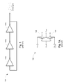
- Fig. 1 shows a schematic diagram for a three-stage inverter-based ring oscillator 100.
- the ring oscillator 100 comprises a chain of three inverters 102a, 102b, and 102c connected in cascade fashion. The output of last inverter 102c feeds back into the input of the first inverter 102a.
- Inverter-based ring oscillators can be constructed with any odd number of inverters.
- Fig. 1A is a circuit diagram of a typical inverter cell 102 that may be used for inverters 102a, 102b, and 102c in the ring oscillator 100 shown in Fig. 1 .
- the inverter cell 102 comprises a first transistor 122 and a second transistor 124.
- the transistors 122 and 124 may be Field Effect Transistors (FETs).
- FETs Field Effect Transistors
- a gate G of each transistor 122 and 124 is connected to an input terminal V in of the inverter cell 112.
- a drain D of each transistor 122 and 124 is connected to an output terminal V OUT of the inverter cell 102.
- a source S of transistor 122 is configured for connection to a first voltage potential; e.g., V SS .
- a source S of transistor 124 is configured for connection to a second voltage accommodation, e.g., V DD .
- inverter-based ring oscillators are designed with increasingly smaller device sizes in order to maintain reasonable levels of power consumption.
- device noise in ring oscillators become significant.
- One kind of noise called “flicker noise,” which occurs in most electronic devices, is dominant at low frequencies.
- flicker noise can predominate at frequencies as high as about 10 MHz - 20 MHz.
- thermal noise tends to predominate.
- the flicker noise is the predominant noise source, and can manifest itself in the output signal of the ring oscillator as phase noise (frequency domain) or jitter (time domain).
- GB 2 050 097 A discloses a voltage control circuit having a supply voltage source which provides a supply voltage controlled in accordance with temperature.
- a ring oscillator is described which is based on a cascade CMOS inverters.
- a ring oscillator includes a number of inverter cells connected in cascade fashion. An output of each inverter cell is connected to an input of another inverter cell. Each inverter cell includes first and second resistors for connection to respective first and second voltage potentials. An output of the ring oscillator is an oscillatory signal having a frequency that is based at least on the resistance values of the first and second resistors.
- each inverter cell includes first and second transistors. Sources of the first and second transistors are connected to the first and second resistors, respectively.
- each inverter cell further includes a capacitor connected to the first and second transistors.
- a phase locked loop comprises a ring oscillator in accordance with the present disclosure.
- a frequency divider circuit comprises a ring oscillator in accordance with the present disclosure.
- an inverter cell 202 in accordance with embodiments of the present disclosure comprises a first transistor M 1 and a second transistor M 2 , and a first resistor R 1 and a second resistor R 2 .
- the transistors M 1 and M 2 may be FETs; e.g., Metal Oxide Semiconductor FETs (MOSFETs).
- MOSFETs Metal Oxide Semiconductor FETs
- the transistor M 1 is an N-channel MOSFET and the transistor M 2 is a P-channel MOSFET. It will be appreciated of course that other combinations of transistor types for M 1 and M 2 may be employed.
- An input terminal V in of the inverter cell 202 is connected to a gate G of each transistor M 1 and M 2 .
- An output terminal V OUT of the inverter cell 202 is connected to a drain D of each transistor M 1 and M 2 .
- a source S of transistor M 1 is connected to a first terminal 212 of resistor R 1 .
- a second terminal 214 of resistor R 1 may be connected to a first power rail 222 that is configured for connection to a first voltage potential; e.g., V SS .
- a source S of transistor M 2 is connected to a first terminal 216 of resistor R 2 .
- a second terminal 218 of resistor R 2 may be connected to a second power rail 224 that is configured for connection to a second voltage potential; e.g., V DD .
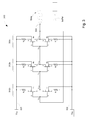
- Fig. 3 illustrates an embodiment of a ring oscillator 300 comprising inverter cells 302a, 302b, and 302c of the form shown in Fig. 2 .
- the inverter cells 302a, 302b, and 302c are connected in cascade fashion. Accordingly, the output V OUT of cell 302a is fed into the input V in of cell 302b. The output V OUT of cell 302b is fed into the input V in of cell 302c. The output V OUT of cell 302c is fed back into the input V in of cell 302a.
- each cell 302a, 302b, and 302c may be connected to respective power rails 322 and 324 to provide power to the ring oscillator 300.
- the power rails 322 and 324 may be at respective first and second voltage potentials (e.g., V SS and V DD ).
- the ring oscillator 300 may include additional cells.
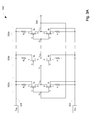
- Fig. 3A illustrates a more generic ring oscillator design 300' comprising some number of stages 302a through 302n other than the three stages shown in Fig. 3 .
- the number of stages 302a through 302n may be an even number or an odd number.
- the ring oscillator 300 shown in Fig. 3 may output an oscillatory signal 304a at a terminal 304.
- the resistors R 1 and R 2 can attenuate the level of flicker noise (phase noise) in the output signal 304a as a result of the effect of resistor degeneration.
- the output signal 304a is oscillatory, its shape may not be adequate for use by electronic circuits that the ring oscillator 300 is being used in.
- the output signal 304a may not be a properly formed square (or rectangular) wave or a properly formed sinusoidal wave.
- additional circuitry may be used to produce a suitable waveform.
- the output signal 304a may be further processed by a buffer that can output a properly formed square wave based on the received output signal.
- the frequency of the output signal of the ring oscillator 100 is dependent upon various aspects of the design of the ring oscillator. For example, the number of inverter stages that comprise the ring oscillator 100 affects the frequency. The frequency will decrease as the number of inverter stages increase, because each additional inverter adds to the propagation delay of the signal along the chain of inverters and hence how frequently the output signal will switch between HI and LO logic levels.
- the transconductance (g m ) of the inverters that comprise a ring oscillator 100 is another factor that affects the frequency of the output signal of the ring oscillator.
- the transconductance of a CMOS inverter is a function of the device size of its constituent transistors. Referring to the inverter cell 102 shown in Fig. 1A , for example, the device size of FET transistor 124 is typically specified by its channel dimensions, which may be expressed as the ratio W/L, where W is the FET channel width (W) and L is the FET channel length.
- Fig. 1A shows typical channel dimensions for the FET transistors 122 and 124 of the inverter 102.
- transistor 122 may have a channel dimension of 600/100 and transistor 124 may have a channel dimension of 1200/100.
- the transconductance also affects power consumption in each inverter during operation, and hence power consumption of the ring oscillator 100 as a whole.
- the transconductance of the inverter 202 shown in Fig. 2 is dependent not only on the channel dimensions of FET transistors M 1 and M 2 , but also on the sizes of the resistors R 1 and R 2 .
- the inverters 302a, 302b, and 302c comprising ring oscillator 300 are designed to have substantially the same transconductance as the design of inverter 102 shown in Fig. 1A .
- the transconductance of the particular inverter design shown in Fig. 2 is substantially the same as the transconductance as the design of inverter 102 shown in Fig.
- the channel dimension of FET transistor M 1 is 1200/50
- the channel dimension of FET transistor M 2 is 2400/50
- each resistor R 1 and R 2 is 600 ⁇ .
- the resistors R 1 and R 2 may have different resistance values.
- the inverters 302a, 302b, and 302c use the inverter design of Fig. 2 . Since the ring oscillator 300 is also a three-stage device as is ring oscillator 100, then the output frequency and power consumption performance of both ring oscillators 100 and 300 are about the same. However, the ring oscillator 300 will exhibit attenuated flicker noise, and in particular reduced phase noise.
- Simulations of a three-stage ring oscillator designed using the inverter cell 102 of Fig. 1A and a three-stage ring oscillator designed using the inverter cell 202 of Fig. 2 were compared. Both ring oscillators were designed to produce an output signal in the gigahertz range. The simulations have shown that the ring oscillator based on the inverter cell 202 exhibits a 2.5 dB reduction in phase noise at 10 MHz as compared to the ring oscillator based on the inverter cell 102. Simulations were made using ring oscillators designed for 3-5 GHz output signals with even greater improvement; a 6dB difference in phase noise was noted.
- the resistor degeneration effect in the ring oscillator 300 can be increased to further attenuate phase noise by increasing the sizes of the resistors R 1 and R 2 in the ring oscillator.
- the frequency of the output signal 304a is inversely related to the resistance of the resistors R 1 and R 2 . Therefore, increasing the resistance of resistors R 1 and R 2 in an attempt to further attenuate phase noise will also decrease the frequency of the output signal 304a.
- Fig. 2A shows an embodiment of an inverter cell 212 that is a variation of the inverter cell 202 shown in Fig. 2 , wherein each resistor R 1 and R 2 is designed for 1 K ⁇ to provide additional phase noise attenuation.
- the inverter cell 212 includes a capacitor C to compensate for the reduction in the frequency of the output signal 304a that may result from using bigger resistors R 1 and R 2 .
- the capacitor C has a capacitance of 10 pF.
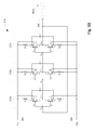
- Fig. 3B shows an embodiment of a ring oscillator 310 comprising inverter cells 312a, 312b, and 312c of the form shown in Fig. 2A .
- the cells 312a, 312b, and 312c are connected in cascade fashion; for example, the output V OUT of cell 312a is fed into the input V in of cell 312b.
- the output V OUT of cell 312b is fed into the input V in of cell 312c.
- the output V OUT of cell 312c is fed back into the input V in of cell 312a.
- the ring oscillator 310 may include additional cells. Simulations of this embodiment of the ring oscillator have shown an additional 1dB improvement in the reducing phase noise.
- the inverter cell 202 of Fig. 2 may be used in a crystal oscillator design.
- the inverter cell 202 itself exhibits improved flicker noise performance because of the effect of resistor degeneration provided by resistors R 1 and R 2 . Accordingly, a crystal-based oscillator design that employs the inverter cell 202 may likewise exhibit a similar improvement in reduced flicker noise.
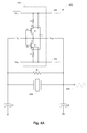
- Fig. 4 illustrates a crystal oscillator 400 in accordance with embodiments of the present disclosure.
- the oscillator 400 comprises a suitable crystal 406.
- a pi ( ⁇ ) network comprising capacitors C1 and C2 may be used to set a resonant frequency in the crystal 406.
- An inverter 402 of the form illustrated in Fig. 2 is connected in parallel with the crystal.
- a resistor R is connected in parallel with the inverter 402 and serves to bias the inverter 402 to operate within its linear region.
- An output terminal 404 of the oscillator 400 may be provided in order to output an oscillatory signal that is generated by the oscillator.
- an oscillator 410 shown in Fig. 4A may include an inverter 412 of the form illustrated in Fig. 2A to attain greater flicker noise attenuation, while maintaining a suitable output frequency.
- the ring oscillator 300 in Fig. 3 may be designed for operation in the gigahertz range.
- the ring oscillator 300 in Fig. 3 may be used in a PLL designed for operation in the range of 10 MHz ⁇ 5MHz.
- the ring oscillator 300 in Fig. 3 may be designed for operation at a corner frequency F c between the region of flicker noise dominance and thermal noise dominance.
- a phase detector 502 receives two inputs: a reference input F ref and feedback from an output F out of a Voltage Controlled Oscillator (VCO) 506. Circuitry for the phase detector 502 is well known.
- the VCO 506 comprises an embodiment of a ring oscillator in accordance with principles of the present invention. In some embodiments, the VCO 506 comprises an embodiment of a crystal oscillator in accordance with principles of the present invention.
- the output of the phase detector 502 is fed to the VCO 506 via filter 504.
- the output of the phase detector 502 controls the VCO 506 such that the phase difference between the two inputs F ref and F out is held constant.
- the filter 504 determines the dynamics of the PLL circuit 500, such as how quickly the PLL circuit 500 responds to changes in the output of the VCO 506.
- a ring oscillator in accordance with principles of the present invention may be embodied in a frequency synthesizer circuit 600.
- a frequency synthesizer may be based on a PLL circuit, for example such as the one depicted in Fig. 5 .
- a phase detector 602 receives two inputs: a reference input F ref and feedback based on an output F out of a VCO 606.
- the VCO 606 comprises an embodiment of a ring oscillator in accordance with principles of the present invention.
- the VCO 606 comprises an embodiment of a crystal oscillator in accordance with principles of the present invention.
- the output of the phase detector 602 is fed to the VCO 606 via filter 604.
- the output of the phase detector 602 controls the VCO 606 such that the phase difference between the two inputs F ref and F out ' is held constant.
- the filter 604 determines the dynamics of the PLL circuit 600, such as how quickly the PLL circuit 600 responds to changes in the output of the VCO 606.
Landscapes
- Physics & Mathematics (AREA)
- Engineering & Computer Science (AREA)
- Computer Hardware Design (AREA)
- Computing Systems (AREA)
- General Engineering & Computer Science (AREA)
- Mathematical Physics (AREA)
- Oscillators With Electromechanical Resonators (AREA)
Description
- The present disclosure claims priority to
U.S. Provisional App. No. 61/376,391 filed on August 24, 2010 - The present invention relates to oscillator circuits and in particular to a low noise CMOS ring oscillator.
- Unless otherwise indicated herein, the approaches described in this section are not prior art to the claims in this application and are not admitted to be prior art by inclusion in this section.
- Complimentary Metal Oxide Semiconductor (CMOS) ring oscillators are widely used in Phase Locked Loop (PLL) circuits. PLLs are commonly used for clock and data recovery, frequency synthesis, clock generation circuitry, etc. Among the various types of CMOS ring oscillators, inverter based single ended or differential ring oscillators are recognized as being efficient and are often the ring oscillator design of choice.
-
Fig. 1 shows a schematic diagram for a three-stage inverter-basedring oscillator 100. Thering oscillator 100 comprises a chain of threeinverters last inverter 102c feeds back into the input of thefirst inverter 102a. Inverter-based ring oscillators can be constructed with any odd number of inverters. -
Fig. 1A is a circuit diagram of atypical inverter cell 102 that may be used forinverters ring oscillator 100 shown inFig. 1 . Theinverter cell 102 comprises afirst transistor 122 and asecond transistor 124. Thetransistors transistor transistor inverter cell 102. A source S oftransistor 122 is configured for connection to a first voltage potential; e.g., VSS. A source S oftransistor 124 is configured for connection to a second voltage potentiel, e.g., VDD. - As semiconductor manufacturing processes continue to shrink and the requirements for higher switching speeds continue to increase, inverter-based ring oscillators are designed with increasingly smaller device sizes in order to maintain reasonable levels of power consumption. As device dimensions decrease, device noise in ring oscillators become significant. One kind of noise called "flicker noise," which occurs in most electronic devices, is dominant at low frequencies. For inverter-based ring oscillator devices using deep submicron processes like 45nm processes or 30nm processes, flicker noise can predominate at frequencies as high as about 10 MHz - 20 MHz. For frequencies above a corner frequency of 10 MHz to 20 MHz, "thermal noise" tends to predominate. For circuit applications that run at 1 MHz to 10 MHz, the flicker noise is the predominant noise source, and can manifest itself in the output signal of the ring oscillator as phase noise (frequency domain) or jitter (time domain).
-
GB 2 050 097 A - It is in the object of the present invention to provide an improved ring oscillator, and a method for operating same.
- The object is solved by the subject matter of the independent claims. Preferred embodiments of the present invention are defined by the dependent claims.
- The present invention is defined by independent claims 1 and 7. In accordance with the invention, a ring oscillator includes a number of inverter cells connected in cascade fashion. An output of each inverter cell is connected to an input of another inverter cell. Each inverter cell includes first and second resistors for connection to respective first and second voltage potentials. An output of the ring oscillator is an oscillatory signal having a frequency that is based at least on the resistance values of the first and second resistors.
- In accordance with the invention, each inverter cell includes first and second transistors. Sources of the first and second transistors are connected to the first and second resistors, respectively.
- In accordance with the invention, each inverter cell further includes a capacitor connected to the first and second transistors.
- In an embodiment, a phase locked loop comprises a ring oscillator in accordance with the present disclosure. In another embodiment, a frequency divider circuit comprises a ring oscillator in accordance with the present disclosure.
- The following detailed description and accompanying drawings provide a better understanding of the nature and advantages of the present invention.
-
-
Fig. 1 illustrates a ring oscillator. -
Fig. 1A shows details for an inverter cell. -
Figs. 2 and 2A shows details for inverter cells in accordance with the present disclosure. -
Figs. 3 ,3A , and3B illustrate embodiments of ring oscillators in accordance with the principles of the present invention. -
Figs. 4 and4A illustrate embodiments of crystal oscillators in accordance with the principles of the present invention. -
Fig. 5 is a block diagram of a phase locked loop in accordance with the present disclosure. -
Fig. 6 , is a block diagram of a frequency divider circuit in accordance with the present disclosure. - The embodiments shown in
figures 2 ,3 ,3A , and4 are useful for understanding the claimed invention but do not form part of the claimed invention. - In the following description, for purposes of explanation, numerous examples and specific details are set forth in order to provide a thorough understanding of the present invention. It will be evident, however, to one skilled in the art that the present invention as defined by the claims may include some or all of the features in these examples alone or in combination with other features described below, and may further include modifications and equivalents of the features and concepts described herein.
- Referring to
Fig. 2 , aninverter cell 202 in accordance with embodiments of the present disclosure comprises a first transistor M1 and a second transistor M2, and a first resistor R1 and a second resistor R2. The transistors M1 and M2 may be FETs; e.g., Metal Oxide Semiconductor FETs (MOSFETs). In an embodiment, the transistor M1 is an N-channel MOSFET and the transistor M2 is a P-channel MOSFET. It will be appreciated of course that other combinations of transistor types for M1 and M2 may be employed. - An input terminal Vin of the
inverter cell 202 is connected to a gate G of each transistor M1 and M2. An output terminal VOUT of theinverter cell 202 is connected to a drain D of each transistor M1 and M2. A source S of transistor M1 is connected to afirst terminal 212 of resistor R1. Asecond terminal 214 of resistor R1 may be connected to afirst power rail 222 that is configured for connection to a first voltage potential; e.g., VSS. A source S of transistor M2 is connected to afirst terminal 216 of resistor R2. Asecond terminal 218 of resistor R2 may be connected to asecond power rail 224 that is configured for connection to a second voltage potential; e.g., VDD. -
Fig. 3 illustrates an embodiment of aring oscillator 300 comprisinginverter cells Fig. 2 . In some embodiments, theinverter cells cell 302a is fed into the input Vin ofcell 302b. The output VOUT ofcell 302b is fed into the input Vin ofcell 302c. The output VOUT ofcell 302c is fed back into the input Vin ofcell 302a. The resistors R1 and R2 of eachcell respective power rails ring oscillator 300. The power rails 322 and 324, in turn, may be at respective first and second voltage potentials (e.g., VSS and VDD). In some embodiments, thering oscillator 300 may include additional cells. For example,Fig. 3A illustrates a more generic ring oscillator design 300' comprising some number ofstages 302a through 302n other than the three stages shown inFig. 3 . The number ofstages 302a through 302n may be an even number or an odd number. - The
ring oscillator 300 shown inFig. 3 may output anoscillatory signal 304a at a terminal 304. The resistors R1 and R2 can attenuate the level of flicker noise (phase noise) in theoutput signal 304a as a result of the effect of resistor degeneration. Though theoutput signal 304a is oscillatory, its shape may not be adequate for use by electronic circuits that thering oscillator 300 is being used in. For example, theoutput signal 304a may not be a properly formed square (or rectangular) wave or a properly formed sinusoidal wave. Accordingly, additional circuitry may be used to produce a suitable waveform. For instance, theoutput signal 304a may be further processed by a buffer that can output a properly formed square wave based on the received output signal. - Referring back to
Figs. 1 and 1A , the frequency of the output signal of thering oscillator 100 is dependent upon various aspects of the design of the ring oscillator. For example, the number of inverter stages that comprise thering oscillator 100 affects the frequency. The frequency will decrease as the number of inverter stages increase, because each additional inverter adds to the propagation delay of the signal along the chain of inverters and hence how frequently the output signal will switch between HI and LO logic levels. - The transconductance (gm) of the inverters that comprise a
ring oscillator 100 is another factor that affects the frequency of the output signal of the ring oscillator. The transconductance of a CMOS inverter is a function of the device size of its constituent transistors. Referring to theinverter cell 102 shown inFig. 1A , for example, the device size ofFET transistor 124 is typically specified by its channel dimensions, which may be expressed as the ratio W/L, where W is the FET channel width (W) and L is the FET channel length.Fig. 1A shows typical channel dimensions for theFET transistors inverter 102. For example,transistor 122 may have a channel dimension of 600/100 andtransistor 124 may have a channel dimension of 1200/100. The transconductance also affects power consumption in each inverter during operation, and hence power consumption of thering oscillator 100 as a whole. - Referring now to
Figs. 2 and3 , in accordance with embodiments of the present disclosure, the transconductance of theinverter 202 shown inFig. 2 is dependent not only on the channel dimensions of FET transistors M1 and M2, but also on the sizes of the resistors R1 and R2. Suppose theinverters ring oscillator 300 are designed to have substantially the same transconductance as the design ofinverter 102 shown inFig. 1A . For example, the transconductance of the particular inverter design shown inFig. 2 is substantially the same as the transconductance as the design ofinverter 102 shown inFig. 1A , where the channel dimension of FET transistor M1 is 1200/50, the channel dimension of FET transistor M2 is 2400/50, and each resistor R1 and R2 is 600 Ω. In other embodiments, the resistors R1 and R2 may have different resistance values. Suppose theinverters Fig. 2 . Since thering oscillator 300 is also a three-stage device as isring oscillator 100, then the output frequency and power consumption performance of bothring oscillators ring oscillator 300 will exhibit attenuated flicker noise, and in particular reduced phase noise. - Simulations of a three-stage ring oscillator designed using the
inverter cell 102 ofFig. 1A and a three-stage ring oscillator designed using theinverter cell 202 ofFig. 2 were compared. Both ring oscillators were designed to produce an output signal in the gigahertz range. The simulations have shown that the ring oscillator based on theinverter cell 202 exhibits a 2.5 dB reduction in phase noise at 10 MHz as compared to the ring oscillator based on theinverter cell 102. Simulations were made using ring oscillators designed for 3-5 GHz output signals with even greater improvement; a 6dB difference in phase noise was noted. - In some embodiments, the resistor degeneration effect in the
ring oscillator 300 can be increased to further attenuate phase noise by increasing the sizes of the resistors R1 and R2 in the ring oscillator. However, the frequency of theoutput signal 304a is inversely related to the resistance of the resistors R1 and R2. Therefore, increasing the resistance of resistors R1 and R2 in an attempt to further attenuate phase noise will also decrease the frequency of theoutput signal 304a. -
Fig. 2A shows an embodiment of aninverter cell 212 that is a variation of theinverter cell 202 shown inFig. 2 , wherein each resistor R1 and R2 is designed for 1 KΩ to provide additional phase noise attenuation. Theinverter cell 212 includes a capacitor C to compensate for the reduction in the frequency of theoutput signal 304a that may result from using bigger resistors R1 and R2. In the particular embodiment shown inFig. 2A , the capacitor C has a capacitance of 10 pF. -
Fig. 3B shows an embodiment of aring oscillator 310 comprisinginverter cells Fig. 2A . Thecells cell 312a is fed into the input Vin ofcell 312b. The output VOUT ofcell 312b is fed into the input Vin ofcell 312c. The output VOUT ofcell 312c is fed back into the input Vin ofcell 312a. In some embodiments, thering oscillator 310 may include additional cells. Simulations of this embodiment of the ring oscillator have shown an additional 1dB improvement in the reducing phase noise. - In other embodiments, the
inverter cell 202 ofFig. 2 may be used in a crystal oscillator design. Theinverter cell 202 itself exhibits improved flicker noise performance because of the effect of resistor degeneration provided by resistors R1 and R2. Accordingly, a crystal-based oscillator design that employs theinverter cell 202 may likewise exhibit a similar improvement in reduced flicker noise. -
Fig. 4 illustrates acrystal oscillator 400 in accordance with embodiments of the present disclosure. Theoscillator 400 comprises asuitable crystal 406. A pi (π) network comprising capacitors C1 and C2 may be used to set a resonant frequency in thecrystal 406. Aninverter 402 of the form illustrated inFig. 2 is connected in parallel with the crystal. A resistor R is connected in parallel with theinverter 402 and serves to bias theinverter 402 to operate within its linear region. Anoutput terminal 404 of theoscillator 400 may be provided in order to output an oscillatory signal that is generated by the oscillator. In other embodiments, anoscillator 410 shown inFig. 4A may include aninverter 412 of the form illustrated inFig. 2A to attain greater flicker noise attenuation, while maintaining a suitable output frequency. - In some embodiments, the
ring oscillator 300 inFig. 3 may be designed for operation in the gigahertz range. Thering oscillator 300 inFig. 3 may be used in a PLL designed for operation in the range of 10 MHz ±5MHz. In some embodiments, thering oscillator 300 inFig. 3 may be designed for operation at a corner frequency Fc between the region of flicker noise dominance and thermal noise dominance. - As illustrated in
Fig. 5 , disclosed embodiments of a ring oscillator in accordance with principles of the present invention may be embodied in a PLL circuit 500. Aphase detector 502 receives two inputs: a reference input Fref and feedback from an output Fout of a Voltage Controlled Oscillator (VCO) 506. Circuitry for thephase detector 502 is well known. TheVCO 506 comprises an embodiment of a ring oscillator in accordance with principles of the present invention. In some embodiments, theVCO 506 comprises an embodiment of a crystal oscillator in accordance with principles of the present invention. The output of thephase detector 502 is fed to theVCO 506 viafilter 504. The output of thephase detector 502 controls theVCO 506 such that the phase difference between the two inputs Fref and Fout is held constant. Thefilter 504 determines the dynamics of the PLL circuit 500, such as how quickly the PLL circuit 500 responds to changes in the output of theVCO 506. - As illustrated in
Fig. 6 , a ring oscillator in accordance with principles of the present invention may be embodied in afrequency synthesizer circuit 600. A frequency synthesizer may be based on a PLL circuit, for example such as the one depicted inFig. 5 . Accordingly, aphase detector 602 receives two inputs: a reference input Fref and feedback based on an output Fout of aVCO 606. TheVCO 606 comprises an embodiment of a ring oscillator in accordance with principles of the present invention. In some embodiments, theVCO 606 comprises an embodiment of a crystal oscillator in accordance with principles of the present invention. A programmable divide-by-n network 608 receives two inputs: the output Fout from theVCO 606 and a counter N, and outputs a signal
phase detector 602. The output of thephase detector 602 is fed to theVCO 606 viafilter 604. The output of thephase detector 602 controls theVCO 606 such that the phase difference between the two inputs Fref and Fout' is held constant. Thefilter 604 determines the dynamics of thePLL circuit 600, such as how quickly thePLL circuit 600 responds to changes in the output of theVCO 606. - As used in the description herein and throughout the claims that follow, "a", "an", and "the" includes plural references unless the context clearly dictates otherwise. Also, as used in the description herein and throughout the claims that follow, the meaning of "in" includes "in" and "on" unless the context clearly dictates otherwise.
- The above description illustrates various embodiments of the present invention along with examples of how aspects of the present invention may be implemented. The above examples and embodiments should not be deemed to be the only embodiments, and are presented to illustrate the flexibility and advantages of the present invention as defined by the following claims. Based on the above disclosure and the following claims, other arrangements, embodiments, implementations and equivalents will be evident to those skilled in the art and may be employed without departing from the scope of the invention as defined by the claims.
Claims (7)
- A ring oscillator (310), comprising:a plurality of inverters (312a, 312b, 312c) connected in cascade fashion, wherein an output (VOUT) of each inverter is connected to an input of another inverter; andan output terminal (304) outputting an oscillatory signal (304a) having a frequency,wherein each of the plurality inverters comprises:a first transistor (M1); anda second transistor (M2);
a first resistor (R1) having a first end and a second end, wherein the first end of the first resistor is directly connected to a source of the first transistor, and wherein the second end of the first resistor is directly connected to a first voltage potential (Vss);
a second resistor (R2) having a first end and a second end, wherein the first end of the second resistor is directly connected to a source of the second transistor, and wherein the second end of the second transistor is directly connected to a second voltage potential (VDD), such that the first resistor, the first transistor, the second transistor, and the second resistor form a series connection;characterized in that the ring oscillator further includes:a capacitor (C) having a first end and a second end, wherein the first end of the capacitor is directly connected to each of the source of the first transistor and the first end of the first resistor, and wherein the second end of the capacitor is directly connected to each of the source of the second transistor and the first end of the second resistor, such that the capacitor is connected in parallel with the first transistor and the second transistor, and is connected in series with the first resistor and the second resistor,wherein the frequency of the oscillatory signal is based at least on resistance values of the first resistors and resistance values of the second resistors. - The ring oscillator of claim 1, wherein:a gate of the first transistor and a gate of the second transistor are connected to the input of a respective one of the plurality of inverters, anda drain of the first transistor and a drain of the second transistor are connected to the output of a respective one of the plurality of inverters.
- The ring oscillator of any one of claims 1 to 2 wherein a flicker noise of the ring oscillator is dependent on the resistance values of the first resistors and the second resistors.
- The ring oscillator of claim 1 wherein the capacitor increases an operating frequency of the ring oscillator.
- A phase locked loop comprising the ring oscillator of any one of claims 1 to 4.
- A frequency divider circuit comprising the ring oscillator of any one of claims 1 to 4.
- A method for operating a ring oscillator (310), the method comprising:generating a first output (VOUT) from a first inverter circuit (312a);feeding the first output into a second inverter circuit (312b)to generate a second output (VOUT);feeding the second output into at least a third inverter circuit (312c) to generate a third output (VOUT);feeding the third output into the first inverter circuit, thereby generating the first output; andreducing flicker noise in the ring oscillator by producing a resistor degeneration effect in the first inverter circuit, the second inverter circuit, and the third inverter circuit,where producing the resistor degeneration effect in an inverter includes
providing a first voltage level to a first transistor (M1) of the inverter via a first resistor (R1), the first resistor having (i) a first end directly connected to a source of the first transistor and (ii) a second end directly connected to a first supply (VSS) corresponding to the first voltage level, and
providing a second voltage level to a second transistor (M2) of the inverter via a second resistor (R1), the second resistor having (i) a first end directly connected to a source of a second transistor and (ii) a second end directly connected to a second supply (VDD) corresponding to the second voltage level, such that the first resistor, the first transistor, the second transistor, and the second resistor form a series connection; characterized in thatusing a capacitor (C) connected between the first resistor and the second resistor, increasing an operating frequency of the ring oscillator, wherein the capacitor is connected in parallel with the first transistor and the second transistor, and is connected in series with the first resistor and the second resistor.
Applications Claiming Priority (2)
| Application Number | Priority Date | Filing Date | Title |
|---|---|---|---|
| US37639110P | 2010-08-24 | 2010-08-24 | |
| PCT/US2011/048277 WO2012027199A1 (en) | 2010-08-24 | 2011-08-18 | Low noise cmos ring oscillator |
Publications (3)
| Publication Number | Publication Date |
|---|---|
| EP2609681A1 EP2609681A1 (en) | 2013-07-03 |
| EP2609681A4 EP2609681A4 (en) | 2014-05-07 |
| EP2609681B1 true EP2609681B1 (en) | 2015-07-22 |
Family
ID=45696361
Family Applications (1)
| Application Number | Title | Priority Date | Filing Date |
|---|---|---|---|
| EP11820415.5A Not-in-force EP2609681B1 (en) | 2010-08-24 | 2011-08-18 | Low noise cmos ring oscillator |
Country Status (4)
| Country | Link |
|---|---|
| US (2) | US8624681B2 (en) |
| EP (1) | EP2609681B1 (en) |
| CN (1) | CN103098372B (en) |
| WO (1) | WO2012027199A1 (en) |
Cited By (1)
| Publication number | Priority date | Publication date | Assignee | Title |
|---|---|---|---|---|
| WO2024255935A1 (en) | 2023-06-16 | 2024-12-19 | České vysoké učení technické v Praze | Low flicker noise near-threshold cmos inverter |
Families Citing this family (11)
| Publication number | Priority date | Publication date | Assignee | Title |
|---|---|---|---|---|
| EP2609681B1 (en) * | 2010-08-24 | 2015-07-22 | Marvell World Trade Ltd. | Low noise cmos ring oscillator |
| US20140022023A1 (en) * | 2012-07-20 | 2014-01-23 | Mediatek Inc. | Temperature-insensitive ring oscillators and inverter circuits |
| US9306577B2 (en) | 2013-02-27 | 2016-04-05 | Mediatek Inc. | Supply voltage drift insensitive digitally controlled oscillator and phase locked loop circuit |
| CN104253587B (en) * | 2013-06-27 | 2017-10-20 | 上海东软载波微电子有限公司 | Crystal oscillator |
| JP6314673B2 (en) * | 2014-06-11 | 2018-04-25 | 富士電機株式会社 | Semiconductor device |
| US10295583B2 (en) * | 2015-04-16 | 2019-05-21 | Taiwan Semiconductor Manufacturing Company, Ltd. | Circuit for measuring flicker noise and method of using the same |
| CN106788419A (en) * | 2016-11-22 | 2017-05-31 | 广东技术师范学院 | A kind of high performance adjustable wide band radio-frequency oscilator system |
| CN107830940A (en) * | 2017-10-13 | 2018-03-23 | 京东方科技集团股份有限公司 | A kind of temperature sensor, array base palte, display device |
| US10886901B1 (en) * | 2020-02-14 | 2021-01-05 | Realtek Semiconductor Corp. | Low supply voltage ring oscillator and method thereof |
| WO2022113341A1 (en) * | 2020-11-30 | 2022-06-02 | 三菱電機株式会社 | Voltage-controlled oscillator |
| CN113162616A (en) * | 2021-01-14 | 2021-07-23 | 温州大学 | Ring oscillator |
Family Cites Families (12)
| Publication number | Priority date | Publication date | Assignee | Title |
|---|---|---|---|---|
| JPS55135780A (en) * | 1979-04-10 | 1980-10-22 | Citizen Watch Co Ltd | Electronic watch |
| JP4167747B2 (en) | 1998-04-13 | 2008-10-22 | 株式会社ルネサステクノロジ | Frequency variable oscillation circuit and phase synchronization circuit using the same |
| US6097253A (en) * | 1999-02-12 | 2000-08-01 | Pmc-Sierra Ltd. | High speed process-controlled transresistance amplifier |
| CN2511046Y (en) * | 2001-02-28 | 2002-09-11 | 矽统科技股份有限公司 | High Noise Immunity Low Power Device for Quartz Oscillators |
| US6650191B2 (en) * | 2001-09-07 | 2003-11-18 | Texas Instruments Incorporated | Low jitter ring oscillator architecture |
| US7679463B2 (en) * | 2004-03-22 | 2010-03-16 | Mobius Microsystems, Inc. | Multi-terminal harmonic oscillator integrated circuit with frequency calibration and frequency configuration |
| US7268630B2 (en) | 2005-04-25 | 2007-09-11 | International Business Machines Corporation | Phase-locked loop using continuously auto-tuned inductor-capacitor voltage controlled oscillator |
| US8044727B2 (en) * | 2005-12-20 | 2011-10-25 | Fujitsu Limited | Phased locked loop circuit including voltage controlled ring oscillator |
| US7719373B2 (en) * | 2006-10-27 | 2010-05-18 | Imec | Device and method for generating a signal with predefined transcient at start-up |
| DE102007023044B4 (en) | 2007-05-16 | 2011-02-10 | Texas Instruments Deutschland Gmbh | Ring oscillator for PLLs |
| KR101541733B1 (en) * | 2008-10-09 | 2015-08-04 | 삼성전자주식회사 | Digitally controlled oscillator |
| EP2609681B1 (en) * | 2010-08-24 | 2015-07-22 | Marvell World Trade Ltd. | Low noise cmos ring oscillator |
-
2011
- 2011-08-18 EP EP11820415.5A patent/EP2609681B1/en not_active Not-in-force
- 2011-08-18 US US13/212,771 patent/US8624681B2/en active Active
- 2011-08-18 CN CN201180040936.1A patent/CN103098372B/en not_active Expired - Fee Related
- 2011-08-18 WO PCT/US2011/048277 patent/WO2012027199A1/en not_active Ceased
-
2014
- 2014-01-07 US US14/149,073 patent/US9148131B2/en active Active
Cited By (1)
| Publication number | Priority date | Publication date | Assignee | Title |
|---|---|---|---|---|
| WO2024255935A1 (en) | 2023-06-16 | 2024-12-19 | České vysoké učení technické v Praze | Low flicker noise near-threshold cmos inverter |
Also Published As
| Publication number | Publication date |
|---|---|
| US8624681B2 (en) | 2014-01-07 |
| CN103098372B (en) | 2016-03-02 |
| WO2012027199A1 (en) | 2012-03-01 |
| US9148131B2 (en) | 2015-09-29 |
| EP2609681A1 (en) | 2013-07-03 |
| US20140118077A1 (en) | 2014-05-01 |
| CN103098372A (en) | 2013-05-08 |
| EP2609681A4 (en) | 2014-05-07 |
| US20120049964A1 (en) | 2012-03-01 |
Similar Documents
| Publication | Publication Date | Title |
|---|---|---|
| US8624681B2 (en) | Low noise CMOS ring oscillator | |
| US7522008B2 (en) | Injection locker frequency divider | |
| CN101557213B (en) | Delay unit, annular oscillator and PLL circuit | |
| JP5876368B2 (en) | Phase-locked loop circuit having a voltage controlled oscillator with improved bandwidth | |
| US8264290B2 (en) | Dual positive-feedbacks voltage controlled oscillator | |
| WO2010093530A3 (en) | Integrated voltage-controlled oscillator circuits | |
| US7863991B1 (en) | Wide range/high speed low power CMOS VCO | |
| Hemmati et al. | Novel six‐phase ring voltage controlled oscillator with wide frequency tuning range | |
| US8120429B1 (en) | Voltage-controlled oscillator methods and apparatus | |
| US8035453B1 (en) | Techniques relating to oscillators | |
| Nishchal et al. | Design of novel phase frequency detectors for low phase noise frequency multipliers | |
| US8729931B1 (en) | Divide-by-two divider circuit having branches with static current blocking circuits | |
| US7132903B1 (en) | Noise-shielding, switch-controlled load circuitry for oscillators and the like | |
| US6774733B2 (en) | Frequency variable oscillation circuit | |
| US6861911B2 (en) | Self-regulating voltage controlled oscillator | |
| Zhang et al. | Process variation compensated voltage controlled ring oscillator with subtraction-based voltage controlled current source | |
| Tran et al. | An ultra-low power consumption and very compact 1.49 GHz CMOS voltage controlled ring oscillator | |
| Sharma et al. | Design of a hybrid ring oscillator at 1.5/3.0 GHz with low power supply sensitivity | |
| Hong et al. | Low-power CMOS injection-locked and current-mode logic frequency dividers in a 50 GHz LC cross-coupled oscillator | |
| Jiang et al. | Model analysis of multi-finger MOSFET layout in ring oscillator design | |
| KR20080083661A (en) | High-frequency power supply circuit | |
| JP2010056829A (en) | Oscillation circuit | |
| Saini et al. | Differential ring voltage controlled oscillator-A review | |
| Ann et al. | Low power CMOS 8: 1 injection-locked frequency divider with LC cross-coupled oscillator | |
| JP2007208589A (en) | Frequency divider |
Legal Events
| Date | Code | Title | Description |
|---|---|---|---|
| PUAI | Public reference made under article 153(3) epc to a published international application that has entered the european phase |
Free format text: ORIGINAL CODE: 0009012 |
|
| 17P | Request for examination filed |
Effective date: 20130225 |
|
| AK | Designated contracting states |
Kind code of ref document: A1 Designated state(s): AL AT BE BG CH CY CZ DE DK EE ES FI FR GB GR HR HU IE IS IT LI LT LU LV MC MK MT NL NO PL PT RO RS SE SI SK SM TR |
|
| DAX | Request for extension of the european patent (deleted) | ||
| A4 | Supplementary search report drawn up and despatched |
Effective date: 20140407 |
|
| RIC1 | Information provided on ipc code assigned before grant |
Ipc: H03K 3/03 20060101AFI20140401BHEP |
|
| GRAP | Despatch of communication of intention to grant a patent |
Free format text: ORIGINAL CODE: EPIDOSNIGR1 |
|
| INTG | Intention to grant announced |
Effective date: 20150318 |
|
| RIN1 | Information on inventor provided before grant (corrected) |
Inventor name: GUO, ZHENDONG Inventor name: MING, JUN |
|
| GRAS | Grant fee paid |
Free format text: ORIGINAL CODE: EPIDOSNIGR3 |
|
| GRAA | (expected) grant |
Free format text: ORIGINAL CODE: 0009210 |
|
| AK | Designated contracting states |
Kind code of ref document: B1 Designated state(s): AL AT BE BG CH CY CZ DE DK EE ES FI FR GB GR HR HU IE IS IT LI LT LU LV MC MK MT NL NO PL PT RO RS SE SI SK SM TR |
|
| REG | Reference to a national code |
Ref country code: GB Ref legal event code: FG4D |
|
| REG | Reference to a national code |
Ref country code: CH Ref legal event code: EP |
|
| REG | Reference to a national code |
Ref country code: IE Ref legal event code: FG4D |
|
| REG | Reference to a national code |
Ref country code: AT Ref legal event code: REF Ref document number: 738389 Country of ref document: AT Kind code of ref document: T Effective date: 20150815 |
|
| REG | Reference to a national code |
Ref country code: DE Ref legal event code: R096 Ref document number: 602011018106 Country of ref document: DE |
|
| REG | Reference to a national code |
Ref country code: AT Ref legal event code: MK05 Ref document number: 738389 Country of ref document: AT Kind code of ref document: T Effective date: 20150722 |
|
| REG | Reference to a national code |
Ref country code: LT Ref legal event code: MG4D |
|
| REG | Reference to a national code |
Ref country code: NL Ref legal event code: MP Effective date: 20150722 |
|
| PG25 | Lapsed in a contracting state [announced via postgrant information from national office to epo] |
Ref country code: GR Free format text: LAPSE BECAUSE OF FAILURE TO SUBMIT A TRANSLATION OF THE DESCRIPTION OR TO PAY THE FEE WITHIN THE PRESCRIBED TIME-LIMIT Effective date: 20151023 Ref country code: LV Free format text: LAPSE BECAUSE OF FAILURE TO SUBMIT A TRANSLATION OF THE DESCRIPTION OR TO PAY THE FEE WITHIN THE PRESCRIBED TIME-LIMIT Effective date: 20150722 Ref country code: LT Free format text: LAPSE BECAUSE OF FAILURE TO SUBMIT A TRANSLATION OF THE DESCRIPTION OR TO PAY THE FEE WITHIN THE PRESCRIBED TIME-LIMIT Effective date: 20150722 Ref country code: FI Free format text: LAPSE BECAUSE OF FAILURE TO SUBMIT A TRANSLATION OF THE DESCRIPTION OR TO PAY THE FEE WITHIN THE PRESCRIBED TIME-LIMIT Effective date: 20150722 Ref country code: NO Free format text: LAPSE BECAUSE OF FAILURE TO SUBMIT A TRANSLATION OF THE DESCRIPTION OR TO PAY THE FEE WITHIN THE PRESCRIBED TIME-LIMIT Effective date: 20151022 |
|
| PG25 | Lapsed in a contracting state [announced via postgrant information from national office to epo] |
Ref country code: SE Free format text: LAPSE BECAUSE OF FAILURE TO SUBMIT A TRANSLATION OF THE DESCRIPTION OR TO PAY THE FEE WITHIN THE PRESCRIBED TIME-LIMIT Effective date: 20150722 Ref country code: PT Free format text: LAPSE BECAUSE OF FAILURE TO SUBMIT A TRANSLATION OF THE DESCRIPTION OR TO PAY THE FEE WITHIN THE PRESCRIBED TIME-LIMIT Effective date: 20151123 Ref country code: RS Free format text: LAPSE BECAUSE OF FAILURE TO SUBMIT A TRANSLATION OF THE DESCRIPTION OR TO PAY THE FEE WITHIN THE PRESCRIBED TIME-LIMIT Effective date: 20150722 Ref country code: PL Free format text: LAPSE BECAUSE OF FAILURE TO SUBMIT A TRANSLATION OF THE DESCRIPTION OR TO PAY THE FEE WITHIN THE PRESCRIBED TIME-LIMIT Effective date: 20150722 Ref country code: ES Free format text: LAPSE BECAUSE OF FAILURE TO SUBMIT A TRANSLATION OF THE DESCRIPTION OR TO PAY THE FEE WITHIN THE PRESCRIBED TIME-LIMIT Effective date: 20150722 Ref country code: HR Free format text: LAPSE BECAUSE OF FAILURE TO SUBMIT A TRANSLATION OF THE DESCRIPTION OR TO PAY THE FEE WITHIN THE PRESCRIBED TIME-LIMIT Effective date: 20150722 Ref country code: IS Free format text: LAPSE BECAUSE OF FAILURE TO SUBMIT A TRANSLATION OF THE DESCRIPTION OR TO PAY THE FEE WITHIN THE PRESCRIBED TIME-LIMIT Effective date: 20151122 Ref country code: AT Free format text: LAPSE BECAUSE OF FAILURE TO SUBMIT A TRANSLATION OF THE DESCRIPTION OR TO PAY THE FEE WITHIN THE PRESCRIBED TIME-LIMIT Effective date: 20150722 |
|
| REG | Reference to a national code |
Ref country code: CH Ref legal event code: PL |
|
| REG | Reference to a national code |
Ref country code: DE Ref legal event code: R097 Ref document number: 602011018106 Country of ref document: DE |
|
| PG25 | Lapsed in a contracting state [announced via postgrant information from national office to epo] |
Ref country code: DK Free format text: LAPSE BECAUSE OF FAILURE TO SUBMIT A TRANSLATION OF THE DESCRIPTION OR TO PAY THE FEE WITHIN THE PRESCRIBED TIME-LIMIT Effective date: 20150722 Ref country code: EE Free format text: LAPSE BECAUSE OF FAILURE TO SUBMIT A TRANSLATION OF THE DESCRIPTION OR TO PAY THE FEE WITHIN THE PRESCRIBED TIME-LIMIT Effective date: 20150722 Ref country code: SK Free format text: LAPSE BECAUSE OF FAILURE TO SUBMIT A TRANSLATION OF THE DESCRIPTION OR TO PAY THE FEE WITHIN THE PRESCRIBED TIME-LIMIT Effective date: 20150722 Ref country code: IT Free format text: LAPSE BECAUSE OF FAILURE TO SUBMIT A TRANSLATION OF THE DESCRIPTION OR TO PAY THE FEE WITHIN THE PRESCRIBED TIME-LIMIT Effective date: 20150722 Ref country code: CZ Free format text: LAPSE BECAUSE OF FAILURE TO SUBMIT A TRANSLATION OF THE DESCRIPTION OR TO PAY THE FEE WITHIN THE PRESCRIBED TIME-LIMIT Effective date: 20150722 Ref country code: CH Free format text: LAPSE BECAUSE OF NON-PAYMENT OF DUE FEES Effective date: 20150831 Ref country code: MC Free format text: LAPSE BECAUSE OF FAILURE TO SUBMIT A TRANSLATION OF THE DESCRIPTION OR TO PAY THE FEE WITHIN THE PRESCRIBED TIME-LIMIT Effective date: 20150722 Ref country code: LI Free format text: LAPSE BECAUSE OF NON-PAYMENT OF DUE FEES Effective date: 20150831 |
|
| PLBE | No opposition filed within time limit |
Free format text: ORIGINAL CODE: 0009261 |
|
| STAA | Information on the status of an ep patent application or granted ep patent |
Free format text: STATUS: NO OPPOSITION FILED WITHIN TIME LIMIT |
|
| PG25 | Lapsed in a contracting state [announced via postgrant information from national office to epo] |
Ref country code: RO Free format text: LAPSE BECAUSE OF FAILURE TO SUBMIT A TRANSLATION OF THE DESCRIPTION OR TO PAY THE FEE WITHIN THE PRESCRIBED TIME-LIMIT Effective date: 20150722 |
|
| REG | Reference to a national code |
Ref country code: IE Ref legal event code: MM4A |
|
| 26N | No opposition filed |
Effective date: 20160425 |
|
| PG25 | Lapsed in a contracting state [announced via postgrant information from national office to epo] |
Ref country code: IE Free format text: LAPSE BECAUSE OF NON-PAYMENT OF DUE FEES Effective date: 20150818 |
|
| REG | Reference to a national code |
Ref country code: FR Ref legal event code: PLFP Year of fee payment: 6 |
|
| PG25 | Lapsed in a contracting state [announced via postgrant information from national office to epo] |
Ref country code: SI Free format text: LAPSE BECAUSE OF FAILURE TO SUBMIT A TRANSLATION OF THE DESCRIPTION OR TO PAY THE FEE WITHIN THE PRESCRIBED TIME-LIMIT Effective date: 20150722 |
|
| PG25 | Lapsed in a contracting state [announced via postgrant information from national office to epo] |
Ref country code: MT Free format text: LAPSE BECAUSE OF FAILURE TO SUBMIT A TRANSLATION OF THE DESCRIPTION OR TO PAY THE FEE WITHIN THE PRESCRIBED TIME-LIMIT Effective date: 20150722 |
|
| PG25 | Lapsed in a contracting state [announced via postgrant information from national office to epo] |
Ref country code: HU Free format text: LAPSE BECAUSE OF FAILURE TO SUBMIT A TRANSLATION OF THE DESCRIPTION OR TO PAY THE FEE WITHIN THE PRESCRIBED TIME-LIMIT; INVALID AB INITIO Effective date: 20110818 Ref country code: BG Free format text: LAPSE BECAUSE OF FAILURE TO SUBMIT A TRANSLATION OF THE DESCRIPTION OR TO PAY THE FEE WITHIN THE PRESCRIBED TIME-LIMIT Effective date: 20150722 Ref country code: SM Free format text: LAPSE BECAUSE OF FAILURE TO SUBMIT A TRANSLATION OF THE DESCRIPTION OR TO PAY THE FEE WITHIN THE PRESCRIBED TIME-LIMIT Effective date: 20150722 |
|
| PG25 | Lapsed in a contracting state [announced via postgrant information from national office to epo] |
Ref country code: NL Free format text: LAPSE BECAUSE OF FAILURE TO SUBMIT A TRANSLATION OF THE DESCRIPTION OR TO PAY THE FEE WITHIN THE PRESCRIBED TIME-LIMIT Effective date: 20150722 Ref country code: CY Free format text: LAPSE BECAUSE OF FAILURE TO SUBMIT A TRANSLATION OF THE DESCRIPTION OR TO PAY THE FEE WITHIN THE PRESCRIBED TIME-LIMIT Effective date: 20150722 |
|
| PG25 | Lapsed in a contracting state [announced via postgrant information from national office to epo] |
Ref country code: BE Free format text: LAPSE BECAUSE OF NON-PAYMENT OF DUE FEES Effective date: 20150831 |
|
| REG | Reference to a national code |
Ref country code: FR Ref legal event code: PLFP Year of fee payment: 7 |
|
| PG25 | Lapsed in a contracting state [announced via postgrant information from national office to epo] |
Ref country code: LU Free format text: LAPSE BECAUSE OF NON-PAYMENT OF DUE FEES Effective date: 20150818 |
|
| PG25 | Lapsed in a contracting state [announced via postgrant information from national office to epo] |
Ref country code: TR Free format text: LAPSE BECAUSE OF FAILURE TO SUBMIT A TRANSLATION OF THE DESCRIPTION OR TO PAY THE FEE WITHIN THE PRESCRIBED TIME-LIMIT Effective date: 20150722 Ref country code: MK Free format text: LAPSE BECAUSE OF FAILURE TO SUBMIT A TRANSLATION OF THE DESCRIPTION OR TO PAY THE FEE WITHIN THE PRESCRIBED TIME-LIMIT Effective date: 20150722 |
|
| REG | Reference to a national code |
Ref country code: FR Ref legal event code: PLFP Year of fee payment: 8 |
|
| PG25 | Lapsed in a contracting state [announced via postgrant information from national office to epo] |
Ref country code: AL Free format text: LAPSE BECAUSE OF FAILURE TO SUBMIT A TRANSLATION OF THE DESCRIPTION OR TO PAY THE FEE WITHIN THE PRESCRIBED TIME-LIMIT Effective date: 20150722 |
|
| PGFP | Annual fee paid to national office [announced via postgrant information from national office to epo] |
Ref country code: FR Payment date: 20190827 Year of fee payment: 9 |
|
| REG | Reference to a national code |
Ref country code: DE Ref legal event code: R082 Ref document number: 602011018106 Country of ref document: DE Representative=s name: GRUENECKER PATENT- UND RECHTSANWAELTE PARTG MB, DE Ref country code: DE Ref legal event code: R081 Ref document number: 602011018106 Country of ref document: DE Owner name: MARVELL ASIA PTE, LTD., SG Free format text: FORMER OWNER: MARVELL WORLD TRADE LTD., ST. MICHAEL, BB |
|
| REG | Reference to a national code |
Ref country code: GB Ref legal event code: 732E Free format text: REGISTERED BETWEEN 20200709 AND 20200715 |
|
| PG25 | Lapsed in a contracting state [announced via postgrant information from national office to epo] |
Ref country code: FR Free format text: LAPSE BECAUSE OF NON-PAYMENT OF DUE FEES Effective date: 20200831 |
|
| PGFP | Annual fee paid to national office [announced via postgrant information from national office to epo] |
Ref country code: GB Payment date: 20210826 Year of fee payment: 11 |
|
| PGFP | Annual fee paid to national office [announced via postgrant information from national office to epo] |
Ref country code: DE Payment date: 20211027 Year of fee payment: 11 |
|
| REG | Reference to a national code |
Ref country code: DE Ref legal event code: R119 Ref document number: 602011018106 Country of ref document: DE |
|
| GBPC | Gb: european patent ceased through non-payment of renewal fee |
Effective date: 20220818 |
|
| PG25 | Lapsed in a contracting state [announced via postgrant information from national office to epo] |
Ref country code: DE Free format text: LAPSE BECAUSE OF NON-PAYMENT OF DUE FEES Effective date: 20230301 |
|
| PG25 | Lapsed in a contracting state [announced via postgrant information from national office to epo] |
Ref country code: GB Free format text: LAPSE BECAUSE OF NON-PAYMENT OF DUE FEES Effective date: 20220818 |