EP2606379B1 - Metal detector and ground-penetrating radar hybrid head and manufacturing method thereof - Google Patents
Metal detector and ground-penetrating radar hybrid head and manufacturing method thereof Download PDFInfo
- Publication number
- EP2606379B1 EP2606379B1 EP11818575.0A EP11818575A EP2606379B1 EP 2606379 B1 EP2606379 B1 EP 2606379B1 EP 11818575 A EP11818575 A EP 11818575A EP 2606379 B1 EP2606379 B1 EP 2606379B1
- Authority
- EP
- European Patent Office
- Prior art keywords
- coil
- crossbar
- transmit
- receive
- dipole antenna
- Prior art date
- Legal status (The legal status is an assumption and is not a legal conclusion. Google has not performed a legal analysis and makes no representation as to the accuracy of the status listed.)
- Active
Links
Images






Classifications
-
- G—PHYSICS
- G01—MEASURING; TESTING
- G01V—GEOPHYSICS; GRAVITATIONAL MEASUREMENTS; DETECTING MASSES OR OBJECTS; TAGS
- G01V3/00—Electric or magnetic prospecting or detecting; Measuring magnetic field characteristics of the earth, e.g. declination, deviation
- G01V3/12—Electric or magnetic prospecting or detecting; Measuring magnetic field characteristics of the earth, e.g. declination, deviation operating with electromagnetic waves
-
- G—PHYSICS
- G01—MEASURING; TESTING
- G01V—GEOPHYSICS; GRAVITATIONAL MEASUREMENTS; DETECTING MASSES OR OBJECTS; TAGS
- G01V3/00—Electric or magnetic prospecting or detecting; Measuring magnetic field characteristics of the earth, e.g. declination, deviation
- G01V3/08—Electric or magnetic prospecting or detecting; Measuring magnetic field characteristics of the earth, e.g. declination, deviation operating with magnetic or electric fields produced or modified by objects or geological structures or by detecting devices
- G01V3/10—Electric or magnetic prospecting or detecting; Measuring magnetic field characteristics of the earth, e.g. declination, deviation operating with magnetic or electric fields produced or modified by objects or geological structures or by detecting devices using induction coils
- G01V3/101—Electric or magnetic prospecting or detecting; Measuring magnetic field characteristics of the earth, e.g. declination, deviation operating with magnetic or electric fields produced or modified by objects or geological structures or by detecting devices using induction coils by measuring the impedance of the search coil; by measuring features of a resonant circuit comprising the search coil
-
- G—PHYSICS
- G01—MEASURING; TESTING
- G01V—GEOPHYSICS; GRAVITATIONAL MEASUREMENTS; DETECTING MASSES OR OBJECTS; TAGS
- G01V3/00—Electric or magnetic prospecting or detecting; Measuring magnetic field characteristics of the earth, e.g. declination, deviation
- G01V3/08—Electric or magnetic prospecting or detecting; Measuring magnetic field characteristics of the earth, e.g. declination, deviation operating with magnetic or electric fields produced or modified by objects or geological structures or by detecting devices
- G01V3/10—Electric or magnetic prospecting or detecting; Measuring magnetic field characteristics of the earth, e.g. declination, deviation operating with magnetic or electric fields produced or modified by objects or geological structures or by detecting devices using induction coils
- G01V3/104—Electric or magnetic prospecting or detecting; Measuring magnetic field characteristics of the earth, e.g. declination, deviation operating with magnetic or electric fields produced or modified by objects or geological structures or by detecting devices using induction coils using several coupled or uncoupled coils
- G01V3/105—Electric or magnetic prospecting or detecting; Measuring magnetic field characteristics of the earth, e.g. declination, deviation operating with magnetic or electric fields produced or modified by objects or geological structures or by detecting devices using induction coils using several coupled or uncoupled coils forming directly coupled primary and secondary coils or loops
-
- G—PHYSICS
- G01—MEASURING; TESTING
- G01V—GEOPHYSICS; GRAVITATIONAL MEASUREMENTS; DETECTING MASSES OR OBJECTS; TAGS
- G01V3/00—Electric or magnetic prospecting or detecting; Measuring magnetic field characteristics of the earth, e.g. declination, deviation
- G01V3/15—Electric or magnetic prospecting or detecting; Measuring magnetic field characteristics of the earth, e.g. declination, deviation specially adapted for use during transport, e.g. by a person, vehicle or boat
- G01V3/165—Electric or magnetic prospecting or detecting; Measuring magnetic field characteristics of the earth, e.g. declination, deviation specially adapted for use during transport, e.g. by a person, vehicle or boat operating with magnetic or electric fields produced or modified by the object or by the detecting device
-
- G—PHYSICS
- G01—MEASURING; TESTING
- G01S—RADIO DIRECTION-FINDING; RADIO NAVIGATION; DETERMINING DISTANCE OR VELOCITY BY USE OF RADIO WAVES; LOCATING OR PRESENCE-DETECTING BY USE OF THE REFLECTION OR RERADIATION OF RADIO WAVES; ANALOGOUS ARRANGEMENTS USING OTHER WAVES
- G01S13/00—Systems using the reflection or reradiation of radio waves, e.g. radar systems; Analogous systems using reflection or reradiation of waves whose nature or wavelength is irrelevant or unspecified
- G01S13/88—Radar or analogous systems specially adapted for specific applications
- G01S13/885—Radar or analogous systems specially adapted for specific applications for ground probing
-
- Y—GENERAL TAGGING OF NEW TECHNOLOGICAL DEVELOPMENTS; GENERAL TAGGING OF CROSS-SECTIONAL TECHNOLOGIES SPANNING OVER SEVERAL SECTIONS OF THE IPC; TECHNICAL SUBJECTS COVERED BY FORMER USPC CROSS-REFERENCE ART COLLECTIONS [XRACs] AND DIGESTS
- Y10—TECHNICAL SUBJECTS COVERED BY FORMER USPC
- Y10T—TECHNICAL SUBJECTS COVERED BY FORMER US CLASSIFICATION
- Y10T29/00—Metal working
- Y10T29/49—Method of mechanical manufacture
- Y10T29/49002—Electrical device making
- Y10T29/49016—Antenna or wave energy "plumbing" making
- Y10T29/49018—Antenna or wave energy "plumbing" making with other electrical component
Definitions
- the present disclosure is directed to the field of mine and metal detection and, more particularly, towards systems and methods for integrating a ground penetrating radar head with a metal detector head.
- US 2008/036644 a1 discloses a hybrid found-penetrating radar (GPR) and metal detector (MD) sensor head consisting of a dipole receive coil loop and a transmit coil loop with a GPR planar antenna located in the middle of the coil loops.
- GPR found-penetrating radar
- MD metal detector
- US 2006/055584 A1 discloses a hybrid GPR and MD in which a bow tie planar antenna is spaced apart from tri-axial MD detector coils.
- the sensor must be unintrusive because of the nature of certain underground objects such as land mines.
- the combination of ground penetrating radar (“GPR”) and metal detection (“MD”, also referred to herein as electromagnetic induction, "EMI”, sensing) is desirable because of the different material characteristics that they detect.
- GPR ground penetrating radar
- MD metal detection
- EMI electromagnetic induction
- Integrating the MD sensor coils and the GPR antenna into a single, hybrid head can cause problems because both the transmit and receive coils of the EMI sensor and the antenna of the GPR produce and/or sense electro-magnetic fields that may be affected by the proximity of the other, thereby affecting the operation of the MD, the GPR, or both.
- coupling of the MD coiis to the GPR signal may result in ringing (clutter) in the GPR system, which may lower sensitivity and degrade performance.
- the hybrid head includes at least one GPR antenna, an MD transmit coil, and a MD receive coil that is arranged in a quadrupole configuration including a crossbar to minimize coupling between the transmit and receive coils, similar to common mode rejection.
- the at least one GPR antenna is a planar antenna, such as a V-dipole, that is positioned in a plane perpendicular to the crossbar of the quadrupole receive coil of the MD coils so as to reduce coupling between the GPR antenna and the MD coils.
- the plane in which the MD transmit and receive coils is located is positioned at a non-normal angle between 20 and 90 degrees, and more particularly between 45 and 90 degrees, such as 70 degrees, with respect to a central axis of the GPR planar antenna.
- the hybrid head also includes a V-dipole antenna of a GPR collocated with the MD sensor.
- a V-dipole antenna for a GPR The details of the design and implementation of a V-dipole antenna for a GPR are provided in the papers cited above. Details concerning the design and implementation of V-dipole antennas are also disclosed in Kim et al., "The Design and Realization of a Discreetly Loaded Resistive Vee Dipole on a Printed Circuit Board", 2003, pp. 818-829, Vol. 5089, Proceedings of: SPIE .
- While the configuration discussed above may reduce most of the coupling between the MD sensor and the GPR antenna, there may be some coupling due to components of the MD coils that may be oriented parallel to the to the V-dipoles. This coupling may be reduced by pitching the MD sensor coils at a non-normal angle with respect to the plane of the GPR antenna as discussed above.
- the top and bottom portion of the transmit and receive coils of the MD sensor may be covered by an electrostatic shield.
- the electrostatic shield fixes the capacitance of the coil to a changing outside environment.
- Fig. 1 illustrates a iow radar cross section transmit/receive coil assembly 100.
- the coil assembly 100 is formed from two D-shaped halves 10, 20.
- Each of the halves 10, 20 is formed from a substrate 30 on which a plurality of traces 40 are formed.
- the substrate 30 may be formed from a flexible material such as a polyester or polyimide.
- the traces 40 may be formed of conducting, metallic material such as copper using any known technique, such as chemical etching.
- Connectors 50 connect the traces on the two halves 10,20 such that the current in the receive coil flows in a figure eight pattern through multiple turns of the coil assembly 100, with current flowing through all of the traces 40 on the crossbar 60 in the same direction (referred to in the art as a quadruple configuration).
- the connectors 50 connect the traces 40 such that current flows in the direction of the sequence of arrows A-B-C-D through one turn of the coil assembly 100.
- the transmit coil extends around the outer circumference of both halves 10, 20 on the outside or inside of substrates 30.
- the substrates 30 and the traces 40 are as thin as possible consistent with structural and electrical requirements in order to minimize the radar cross section of the coil assembly 100.
- the transmit coil may be formed in a simple circular pattern on a separate substrate surrounding the receive coil such that the receive coil is concentric with the transmit coil.
- a GPR antenna array 200 including a plurality of elements 210 is shown (3 elements are shown in Fig. 2 , but those of skill in the art will recognize that more or less elements may be used).
- the elements 210 are each planar and in the shape of an inverted V-dipole, with the open end of the V-dipole positioned over the crossbar 60 of the coil assembly 100. In this manner, the components of the coil assembly 100 that are along the B-field axis (i.e., the crossbar 60) do not couple to the V-dipoles 210 which define the E-field axis.
- the elements 210 may be formed on a planar substrate 212 with a metallic trace 220 formed thereon. in Fig.
- the distal ends (the ends at the open end of the V) of the V-dipole elements 210 are positioned such that the crossbar 60 is interposed between them.
- the V-dipole elements 210 are positioned such that no portion of the crossbar 60 is interposed between any portion of the two legs of the V-dipole elements 210. but the distal ends of the V-dipole elements are on opposite sides of the plane in which crossbar 60 is oriented.
- the V-dipole elements are within an imaginary cylinder C (as used herein, "cylinder” is not limited to circular cylinders but rather includes any surface generated by a straight line intersecting and moving along a closed plane curve while remaining parallel to a fixed straight line that is perpendicular to the closed plane curve) with a base formed by the projection of the cross sectional shape of the coil assembly 100 onto the plane which is perpendicular to the planes in which the crossbar 60 and the V-dipole elements 210 are oriented.
- C as used herein, "cylinder” is not limited to circular cylinders but rather includes any surface generated by a straight line intersecting and moving along a closed plane curve while remaining parallel to a fixed straight line that is perpendicular to the closed plane curve
- the receive and transmit coils of the hybrid head 300 are formed by a multilayer PCB (printed circuit board) with through-hole vias for inter-layer connections.
- Each layer of the multi-layer PCB board includes either four grounding (shielding) fingers or two turns each of both the transmit and receive coils.
- the transmit and receive coils arc approximately concentric (as used herein, approximately concentric means that the approximate centers of the receive and transmit coils are both approximately on an axis of concentricity that is normal to the faces of the coils, and one coil is located within an outer perimeter formed by the turns of the other coil).
- the receive coil is in a quadrupole configuration.
- the total numbers of layers included in the PCB board depends upon the number of turns desired.
- Figs. 3A-D illustrate various layers of the PCB.
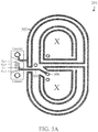
- Fig. 3A illustrates a top grounding (shielding) layer 301 with four grounding fingers formed by a long trace 302 connected to the ground terminal that covers the inner and outer areas of the PCB, and a short trace 304 connected to the Rx- (receive coil negative) terminal and the through hole via 306.
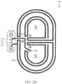
- Fig. 3B illustrates a bottom grounding layer 307 with four grounding fingers formed by the long trace 308, and a short trace 310 connected to the Rx+ (receive coil positive) terminal.
- Each PCB will have one top grounding layer 301 and one bottom grounding layer 307, with one or more pairs of complementary inner layers disposed between them.
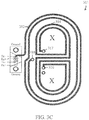
- the first inner layer 311 illustrated in Fig. 3C includes an outer trace 312 that forms two turns of a transmit coil, and an inner trace 314 that forms two turns of a quadrupole receive coil.
- the via 316 in Fig. 3C is aligned with the via 306 in the top grounding layer 301 of Fig. 3A , so the trace 314 will be electrically connected to the Rx- terminal at this point.
- the second inner layer 319 illustrated in Fig. 3D also includes an outer trace 320 that forms two turns of the transmit coil, with one end of the trace connected to the Tx- terminal and the other end connected to via 322 which is aligned with via 318 of Fig. 3C . thereby connecting the two turns of the transmit coil realized by the trace 320 in Fig. 3D to the two turns of the transmit coil realized by the trace 312 of Fig. 3C .
- the second inner layer of Fig. 3D also includes an inner trace 324 that forms two turns of the receive coil in a quadrupole configuration. One end of the trace 324 is connected to via 326, which aligns with via 317 of Fig. 3C .
- a four layer PCB formed by a top layer 301, a first inner layer 311, a second inner layer 319 and a bottom layer 307, along with suitable interconnections made using the vias discussed above, will thus have receive and transmit coils with four turns (two turns on each of the inner layers
- Figs. 4A-F illustrate an exemplary multilayer PCB with internal layers between a top layer and a bottom layer.
- additional vias are added.
- 2 additional vias for the transmit coil and two additional vias for the receive coil are needed for each pair of additional inner layers.
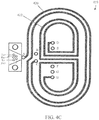
- the six-layer PCB includes a top grounding layer 401 shown in Fig. 4A with a long, four finger grounding trace 402 and a short trace 404 connected to an Rx- terminal via and a second via F.
- Below the top layer 401 is an inner layer 411 shown in Fig. 4B .
- the inner layer 411 includes an outer trace 412 that forms two turns of the transmit coil, and an inner trace 414 that forms two turns of the receive coil, again in a quadruple configuration.
- the outer transmit coil trace 412 is connected on one end to a Tx-terminal via and at the other end to a via C.
- the receive coil turns 414 are connected at one end to a via F (through which it is connected to the Rx- terminal connection in layer 401) and to a via D on the other end.
- the next layer 419 includes two turns 420 of the transmit coil connected to a via C (through which they are connected to the transmit coil turns in layer 411) and a via A, and two turns 422 of the receive coil connected to a via D (through which it is connected to the receive coil turns in layer 411) and a via H.
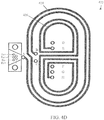
- the next layer 423 shown in Fig. 4D , includes two turns 424 of the transmit coil connected to a via A (through which they arc connected to the transmit coil turns in layer 419) and a via B, and two turns 426 of the receive coil connected to a via H (through which it is connected to the receive coil turns in layer 419) and a via E.
- the next layer 427 shown in Fig.
- the bottom layer 431 shown in Fig. 4F includes a trace 432 connected at one end to a via G (through which it is connected to the receive coil turns in layer 427) and at the other end to a Rx+ terminal.
- the bottom layer 431 also includes a long trace 434 connected to a via 436 that forms four grounding fingers.
- the areas of the PCB marked with an X in Figs. 3A-D inside each of the figure-8 patterns of the receive coil may be removed to allow the distal ends of the V-dipole antennas to be placed through the plane of the PCB.
- those areas in Figs. 3A-D marked with an X are not removed.
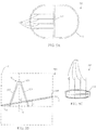
- the layers 301, 307, and one pair of complementary layers 311 and 319 illustrated in Figs. 3A-D may be formed into a single PCB 510 (with the areas of the PCB 510 marked with an X in Figs. 3A-D removed) that forms a part of a hybrid MD/GPR head 500 as shown in Figs. 5A-C . Also forming part of the hybrid head 500 are four planar V-dipole antenna elements 520. As shown most clearly in Fig.
- the legs 522 of each of the antenna elements 520 extend through the central plane (the plane parallel to the faces of the PCB 510 and passing through its center) P of the PCB 510 such that the distal ends of the legs 522 and the vertex V of the elements 520 are on opposite sides of the plane of the PCB 510.
- the central plane P of the PCB 510 forms an angle y of 70 degrees with respect to the central axis Y of the V-dipole antenna elements 520 (the central axis of the V-dipole antenna elements is the axis that passes through the vertex of the V-dipole antenna element and is equidistant from and coplanar with the axes of the two legs of the V-dipole antenna element) and an angle x of 20 degrees with respect to the plane X that is perpendicular to the central axis Y.
- an angle y of 70 degrees is illustrated in Fig.
- the angle y may range from 20 to 90 degrees (i.e., the angle x may range from 0 to 70 degrees) in other embodiments.
- the legs 522 of the V-dipole elements 520 extend through the plane P in the embodiment of Fig. 5
- the entirety of the V-dipole elements 520 are on one side of the plane P while remaining inside an imaginary cylinder C having a cross sectional shape formed by the projection of an outer perimeter of the coils of the PCB 510 on the plane X normal to the central axis of the V-dipole elements 520.
- Positioning the PCB 510 at a non-normal angle with respect to the V-dipole antenna elements 520 reduces antenna coupling by creating a time lag between received impulses in each of the V-dipole antenna legs 522. Since the coupling at each leg and the nearest portions of the PCB 510 are of different length scales, the differential signal between the two is incoherent. The resulting coupling is incoherent and displays little ringing in the received GPR signal. Coupling between the portions of the coils on the PCB 510 that are perpendicular to the legs 522 of the V-dipole elements 520 (e.g., the crossbar 512) is minimized because of the perpendicular relationship.
- the V-dipole elements 520 are on one side of the crossbar 512 (i.e., the elements 420 are on one side of a plane that passes through a center of the crossbar 512, is perpendicular to the faces of the PCB, and is parallel to an axis of the crossbar 512 in a direction in which current flows in the crossbar 512). This is done in order to minimize coupling between the V-dipole elements 520 and the terminals (not shown in Fig. 4 ) of the PCB 510. In other embodiments, V-dipole elements 520 are positioned such that their legs 522 are on opposite sides of the crossbar 512.
- the MD/GPR hybrid heads disclosed herein may be utilized in any device, and in particular may be incorporated into a handheld device that includes the hybrid head and other conventional components such as signal generators to generate signals for transmission by the MD transmit coil and the GPR antenna, a signal processor and associated analog-digital converters to process signals received by the MD receive coil and the GPR antenna, a power supply, and appropriate interconnections between the aforementioned components. Any conventional techniques known in the art may be utilized to process such received signals.
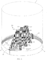
- the handheld device may further incorporate a display for displaying video from the GPR and objects detected by the MD. When the hybrid head is incorporated into such a handheld device, it may be wholly or partially enclosed by a housing such as the housing 600 of Fig. 6 .
- the GPR antenna elements and the transmit and receive coils of the hybrid head will be mechanically connected, either directly to each other or to another component and/or the housing (e.g., the mechanical connections 610 of Fig. 6 ).
Landscapes
- Physics & Mathematics (AREA)
- Life Sciences & Earth Sciences (AREA)
- Engineering & Computer Science (AREA)
- Remote Sensing (AREA)
- Electromagnetism (AREA)
- Environmental & Geological Engineering (AREA)
- Geology (AREA)
- General Life Sciences & Earth Sciences (AREA)
- General Physics & Mathematics (AREA)
- Geophysics (AREA)
- Magnetic Resonance Imaging Apparatus (AREA)
- Variable-Direction Aerials And Aerial Arrays (AREA)
Description
- The present disclosure is directed to the field of mine and metal detection and, more particularly, towards systems and methods for integrating a ground penetrating radar head with a metal detector head.
-
US 2008/036644 a1 discloses a hybrid found-penetrating radar (GPR) and metal detector (MD) sensor head consisting of a dipole receive coil loop and a transmit coil loop with a GPR planar antenna located in the middle of the coil loops. -
US 2006/055584 A1 discloses a hybrid GPR and MD in which a bow tie planar antenna is spaced apart from tri-axial MD detector coils. -
-
Fig. 1 is a schematic representation of the transmit and receive coils of an electromagnetic induction metal detector head according to a disclosed embodiment. -
Fig. 2 is a schematic representation of an integrated ground penetrating radar head according to a disclosed embodiment. -
Figs. 3A-3D are schematic representations of layers in a multi-layer printed circuit board constituting the transmit and receive coils of a metal detector head according to an alternate disclosed embodiment. -
Figs. 4A-4F are schematic representations of layers in a multi-layer printed circuit board constituting the transmit and receive coils of a metal detector head according to an alternate disclosed embodiment. -
Fig. 5A-5C are top view, front view, and side view schematic representations of an integrated ground penetrating radar head according to an alternate disclosed embodiment. -
Fig. 6 is a block diagram of a hybrid head including a printed circuit board implementation of transmit and receive coils and a ground penetrating radar antenna mechanically connected to a housing according to an alternate disclosed embodiment. - A need has arisen for a hand held sensor that can detect underground objects, including but not limited to underground objects such as land mines. The sensor must be unintrusive because of the nature of certain underground objects such as land mines. The combination of ground penetrating radar ("GPR") and metal detection ("MD", also referred to herein as electromagnetic induction, "EMI", sensing) is desirable because of the different material characteristics that they detect. A GPR system can measure the difference between dielectric constants of materials and their relative positions, while the MD measures the nearby presence or absence of conductive materials, with some information about the size and shape.
- Integrating the MD sensor coils and the GPR antenna into a single, hybrid head can cause problems because both the transmit and receive coils of the EMI sensor and the antenna of the GPR produce and/or sense electro-magnetic fields that may be affected by the proximity of the other, thereby affecting the operation of the MD, the GPR, or both. For example, coupling of the MD coiis to the GPR signal may result in ringing (clutter) in the GPR system, which may lower sensitivity and degrade performance. Accordingly, it is desirable to reduce coupling (resonance) between EMI sensor coils and GPR antennas. This can be achieved through both positioning of the coils and antennas relative to each other and through the choice of materials used to fabricate the antennas and coils in the hybrid head.
- At a high level, this disclosure is directed to a GPR and MD hybrid head. In some embodiments, the hybrid head includes at least one GPR antenna, an MD transmit coil, and a MD receive coil that is arranged in a quadrupole configuration including a crossbar to minimize coupling between the transmit and receive coils, similar to common mode rejection. The at least one GPR antenna is a planar antenna, such as a V-dipole, that is positioned in a plane perpendicular to the crossbar of the quadrupole receive coil of the MD coils so as to reduce coupling between the GPR antenna and the MD coils. In some embodiments, in order to further reduce coupling between the GPR antenna and the MD transmit and receive coils, the plane in which the MD transmit and receive coils is located is positioned at a non-normal angle between 20 and 90 degrees, and more particularly between 45 and 90 degrees, such as 70 degrees, with respect to a central axis of the GPR planar antenna.
- The details of the design and implementation of an MD sensor in a quadrupole configuration are discussed in at least the following papers: "Broadband Electromagnetic Induction Sensor for Detecting Buried Landmine," Waymond R. Scott, Jr.: "New Cancellation Technique for Electromagnetic Induction Sensors." Waymond R. Scott, Jr., and Michael Malluck; "Broadband Array of Electromagnetic Induction Sensors for Detecting Buried Landmines," Waymond R. Scott, Jr.; "Location Estimation Using A Broadband Electromagnetic Induction Array," Ali C. Gurbuz, Waymond R. Scott, Jr., and James H. McClellan; "Beamforming Array for Detecting Buried Land Mines," Seung-Ho Lee and Waymond R. Scott, Jr.; "Combined Seismic. Radar, and Induction Sensor for Landmine Detection," Waymond R. Scott, Jr.; Kangwook Kim, Gregg D. Larson, Ali C. Gurbuz, and James H. McClellan; and "Performance Comparison of Frequency Domain Quadrupole and Dipole Electromagnetic Induction Sensors in a Landmine Detection Application," Eric B. Fails, Peter A. Torrione. Waymond R. Scott, Jr., and Leslie M. Collins.
- In addition to the MD sensor arranged in a quadrupole configuration, the hybrid head also includes a V-dipole antenna of a GPR collocated with the MD sensor. The details of the design and implementation of a V-dipole antenna for a GPR are provided in the papers cited above. Details concerning the design and implementation of V-dipole antennas are also disclosed in Kim et al., "The Design and Realization of a Discreetly Loaded Resistive Vee Dipole on a Printed Circuit Board", 2003, pp. 818-829, Vol. 5089, Proceedings of: SPIE.
- While the configuration discussed above may reduce most of the coupling between the MD sensor and the GPR antenna, there may be some coupling due to components of the MD coils that may be oriented parallel to the to the V-dipoles. This coupling may be reduced by pitching the MD sensor coils at a non-normal angle with respect to the plane of the GPR antenna as discussed above.
- Furthermore, in an embodiment the top and bottom portion of the transmit and receive coils of the MD sensor may be covered by an electrostatic shield. The electrostatic shield fixes the capacitance of the coil to a changing outside environment.
- A particular embodiment of an MD/GPR hybrid head will now be discussed with reference to
Figs. 1 and2 .Fig. 1 illustrates a iow radar cross section transmit/receivecoil assembly 100. Thecoil assembly 100 is formed from two D-shaped halves halves substrate 30 on which a plurality oftraces 40 are formed. Thesubstrate 30 may be formed from a flexible material such as a polyester or polyimide. Thetraces 40 may be formed of conducting, metallic material such as copper using any known technique, such as chemical etching.Connectors 50 connect the traces on the twohalves coil assembly 100, with current flowing through all of thetraces 40 on thecrossbar 60 in the same direction (referred to in the art as a quadruple configuration). For example, in one embodiment, theconnectors 50 connect thetraces 40 such that current flows in the direction of the sequence of arrows A-B-C-D through one turn of thecoil assembly 100. The transmit coil extends around the outer circumference of bothhalves substrates 30. Thesubstrates 30 and thetraces 40 are as thin as possible consistent with structural and electrical requirements in order to minimize the radar cross section of thecoil assembly 100. Alternatively, the transmit coil may be formed in a simple circular pattern on a separate substrate surrounding the receive coil such that the receive coil is concentric with the transmit coil. - Referring now to
Fig. 2 , aGPR antenna array 200 including a plurality ofelements 210 is shown (3 elements are shown inFig. 2 , but those of skill in the art will recognize that more or less elements may be used). Theelements 210 are each planar and in the shape of an inverted V-dipole, with the open end of the V-dipole positioned over thecrossbar 60 of thecoil assembly 100. In this manner, the components of thecoil assembly 100 that are along the B-field axis (i.e., the crossbar 60) do not couple to the V-dipoles 210 which define the E-field axis. Theelements 210 may be formed on aplanar substrate 212 with ametallic trace 220 formed thereon. inFig. 2 , the distal ends (the ends at the open end of the V) of the V-dipole elements 210 are positioned such that thecrossbar 60 is interposed between them. In other embodiments, the V-dipole elements 210 are positioned such that no portion of thecrossbar 60 is interposed between any portion of the two legs of the V-dipole elements 210. but the distal ends of the V-dipole elements are on opposite sides of the plane in whichcrossbar 60 is oriented. In such configurations, the V-dipole elements are within an imaginary cylinder C (as used herein, "cylinder" is not limited to circular cylinders but rather includes any surface generated by a straight line intersecting and moving along a closed plane curve while remaining parallel to a fixed straight line that is perpendicular to the closed plane curve) with a base formed by the projection of the cross sectional shape of thecoil assembly 100 onto the plane which is perpendicular to the planes in which thecrossbar 60 and the V-dipole elements 210 are oriented. - A second embodiment of an MD/GPR hybrid head 300 will now be discussed with reference to
Figs. 3A-D and 5A-C . The receive and transmit coils of the hybrid head 300 are formed by a multilayer PCB (printed circuit board) with through-hole vias for inter-layer connections. Each layer of the multi-layer PCB board includes either four grounding (shielding) fingers or two turns each of both the transmit and receive coils. The transmit and receive coils arc approximately concentric (as used herein, approximately concentric means that the approximate centers of the receive and transmit coils are both approximately on an axis of concentricity that is normal to the faces of the coils, and one coil is located within an outer perimeter formed by the turns of the other coil). Also, as above, the receive coil is in a quadrupole configuration. The total numbers of layers included in the PCB board depends upon the number of turns desired. -
Figs. 3A-D illustrate various layers of the PCB.Fig. 3A illustrates a top grounding (shielding)layer 301 with four grounding fingers formed by along trace 302 connected to the ground terminal that covers the inner and outer areas of the PCB, and a short trace 304 connected to the Rx- (receive coil negative) terminal and the through hole via 306.Fig. 3B illustrates abottom grounding layer 307 with four grounding fingers formed by thelong trace 308, and a short trace 310 connected to the Rx+ (receive coil positive) terminal. Each PCB will have onetop grounding layer 301 and onebottom grounding layer 307, with one or more pairs of complementary inner layers disposed between them.Figs. 3C and3D illustrate the complementary first and second inner layer PCBs, respectively. The firstinner layer 311 illustrated inFig. 3C includes an outer trace 312 that forms two turns of a transmit coil, and aninner trace 314 that forms two turns of a quadrupole receive coil. The via 316 inFig. 3C is aligned with the via 306 in thetop grounding layer 301 ofFig. 3A , so thetrace 314 will be electrically connected to the Rx- terminal at this point. - The second
inner layer 319 illustrated inFig. 3D also includes anouter trace 320 that forms two turns of the transmit coil, with one end of the trace connected to the Tx- terminal and the other end connected to via 322 which is aligned with via 318 ofFig. 3C . thereby connecting the two turns of the transmit coil realized by thetrace 320 inFig. 3D to the two turns of the transmit coil realized by the trace 312 ofFig. 3C . The second inner layer ofFig. 3D also includes aninner trace 324 that forms two turns of the receive coil in a quadrupole configuration. One end of thetrace 324 is connected to via 326, which aligns with via 317 ofFig. 3C . thereby connecting the two turns of the receive coil formed by thetrace 324 with the two turns of the receive coil formed by thetrace 314 ofFig. 3C . The other end of thetrace 324 is connected to via 328, which aligns with via 309 of thebottom grounding layer 307 ofFig. 3B , thereby connecting the two turns of the receive coil formed bytrace 324 with the Rx+ terminal shown inFig. 3B . - A four layer PCB formed by a
top layer 301, a firstinner layer 311, a secondinner layer 319 and abottom layer 307, along with suitable interconnections made using the vias discussed above, will thus have receive and transmit coils with four turns (two turns on each of the inner layers - When additional turns on the transmit and receive coils are desired, additional inner PCB layers may be added.
Figs. 4A-F illustrate an exemplary multilayer PCB with internal layers between a top layer and a bottom layer. In order to accommodate the interconnection between the layers, additional vias are added. In general, 2 additional vias for the transmit coil and two additional vias for the receive coil are needed for each pair of additional inner layers. As with the previously discussed 4-layer embodiment, the six-layer PCB includes atop grounding layer 401 shown inFig. 4A with a long, fourfinger grounding trace 402 and ashort trace 404 connected to an Rx- terminal via and a second via F. Below thetop layer 401 is aninner layer 411 shown inFig. 4B . Theinner layer 411 includes anouter trace 412 that forms two turns of the transmit coil, and aninner trace 414 that forms two turns of the receive coil, again in a quadruple configuration. The outer transmitcoil trace 412 is connected on one end to a Tx-terminal via and at the other end to a via C. The receive coil turns 414 are connected at one end to a via F (through which it is connected to the Rx- terminal connection in layer 401) and to a via D on the other end. - The
next layer 419, shown inFig. 4C , includes twoturns 420 of the transmit coil connected to a via C (through which they are connected to the transmit coil turns in layer 411) and a via A, and twoturns 422 of the receive coil connected to a via D (through which it is connected to the receive coil turns in layer 411) and a via H. Thenext layer 423, shown inFig. 4D , includes twoturns 424 of the transmit coil connected to a via A (through which they arc connected to the transmit coil turns in layer 419) and a via B, and twoturns 426 of the receive coil connected to a via H (through which it is connected to the receive coil turns in layer 419) and a via E. Thenext layer 427, shown inFig. 4E , includes twoturns 428 of the transmit coil connected to a via B (through which they are connected to the transmit coil turns in layer 423) and a Tx+ via, and twoturns 430 of the receive coil connected to a via E (through which it is connected to the receive coil turns in layer 423) and a via G. Thebottom layer 431 shown inFig. 4F includes atrace 432 connected at one end to a via G (through which it is connected to the receive coil turns in layer 427) and at the other end to a Rx+ terminal. Thebottom layer 431 also includes along trace 434 connected to a via 436 that forms four grounding fingers. Those of skill will recognize that additional pairs of inner layers may be added by adding additional vias for the transmit and receive coils using the scheme ofFigs. 4A-F . - Referring now back to
Figs. 3A-D , in order to facilitate incorporation of V-dipole antennas (as discussed further below), the areas of the PCB marked with an X inFigs. 3A-D inside each of the figure-8 patterns of the receive coil may be removed to allow the distal ends of the V-dipole antennas to be placed through the plane of the PCB. In other embodiments in which the ends of the V-dipole antennas are not passed through the plane of the PCB, those areas inFigs. 3A-D marked with an X are not removed. - The
layers complementary layers Figs. 3A-D may be formed into a single PCB 510 (with the areas of thePCB 510 marked with an X inFigs. 3A-D removed) that forms a part of a hybrid MD/GPR head 500 as shown inFigs. 5A-C . Also forming part of thehybrid head 500 are four planar V-dipole antenna elements 520. As shown most clearly inFig. 5B , thelegs 522 of each of theantenna elements 520 extend through the central plane (the plane parallel to the faces of thePCB 510 and passing through its center) P of thePCB 510 such that the distal ends of thelegs 522 and the vertex V of theelements 520 are on opposite sides of the plane of thePCB 510. Referring still toFig. 5B , the central plane P of thePCB 510 forms an angle y of 70 degrees with respect to the central axis Y of the V-dipole antenna elements 520 (the central axis of the V-dipole antenna elements is the axis that passes through the vertex of the V-dipole antenna element and is equidistant from and coplanar with the axes of the two legs of the V-dipole antenna element) and an angle x of 20 degrees with respect to the plane X that is perpendicular to the central axis Y. Although an angle y of 70 degrees is illustrated inFig. 5B , the angle y may range from 20 to 90 degrees (i.e., the angle x may range from 0 to 70 degrees) in other embodiments. Further, although thelegs 522 of the V-dipole elements 520 extend through the plane P in the embodiment ofFig. 5 , in other embodiments the entirety of the V-dipole elements 520 are on one side of the plane P while remaining inside an imaginary cylinder C having a cross sectional shape formed by the projection of an outer perimeter of the coils of thePCB 510 on the plane X normal to the central axis of the V-dipole elements 520. - Positioning the
PCB 510 at a non-normal angle with respect to the V-dipole antenna elements 520 reduces antenna coupling by creating a time lag between received impulses in each of the V-dipole antenna legs 522. Since the coupling at each leg and the nearest portions of thePCB 510 are of different length scales, the differential signal between the two is incoherent. The resulting coupling is incoherent and displays little ringing in the received GPR signal. Coupling between the portions of the coils on thePCB 510 that are perpendicular to thelegs 522 of the V-dipole elements 520 (e.g., the crossbar 512) is minimized because of the perpendicular relationship. - Referring now to
Fig. 5A , it can be seen that the V-dipole elements 520 are on one side of the crossbar 512 (i.e., theelements 420 are on one side of a plane that passes through a center of thecrossbar 512, is perpendicular to the faces of the PCB, and is parallel to an axis of thecrossbar 512 in a direction in which current flows in the crossbar 512). This is done in order to minimize coupling between the V-dipole elements 520 and the terminals (not shown inFig. 4 ) of thePCB 510. In other embodiments, V-dipole elements 520 are positioned such that theirlegs 522 are on opposite sides of thecrossbar 512. - The MD/GPR hybrid heads disclosed herein may be utilized in any device, and in particular may be incorporated into a handheld device that includes the hybrid head and other conventional components such as signal generators to generate signals for transmission by the MD transmit coil and the GPR antenna, a signal processor and associated analog-digital converters to process signals received by the MD receive coil and the GPR antenna, a power supply, and appropriate interconnections between the aforementioned components. Any conventional techniques known in the art may be utilized to process such received signals. The handheld device may further incorporate a display for displaying video from the GPR and objects detected by the MD. When the hybrid head is incorporated into such a handheld device, it may be wholly or partially enclosed by a housing such as the
housing 600 ofFig. 6 . Regardless of whether or not a housing is provided, the GPR antenna elements and the transmit and receive coils of the hybrid head will be mechanically connected, either directly to each other or to another component and/or the housing (e.g., themechanical connections 610 ofFig. 6 ). - It will be apparent to those of skill in the art that numerous variations in addition to those discussed above are also possible. Therefore, while the invention has been described with respect to certain specific embodiments, it will be appreciated that many modifications and changes may be made by those skilled in the art without departing from the invention as claimed herein.
Claims (18)
- A ground penetrating radar, GPR, and metal detector, MD, hybrid head comprising: an MD sensor (100) including at least one receive coil (40, 314) in a quadrupole configuration including a crossbar (60), and at least one transmit coil (312), the crossbar having a first axis parallel to a direction in which current flows in the crossbar; and
at least one GPR V-dipole antenna (200) arranged in a plane perpendicular to the first axis of the crossbar so as to reduce coupling between the coils of the MD sensor and the antenna;
wherein the transmit coil has an outer perimeter, the receive coil has an outer perimeter, and wherein at least a portion of the V-dipole antenna is within a cylinder formed by the projection of one of the outer perimeter of the receive coil or the transmit coil onto a plane perpendicular to a central axis of the V-dipole antenna. - The hybrid head of claim 1, further including at least one electrostatic shield covering the top and bottom portion, with respect to the orientation of the head when in use, of the transmit and receive coils so as to stabilize capacitance between the transmit and receive coils and the changing external environment.
- The hybrid head of claim 1 , wherein the at least one receive coil is concentric with the at least one transmit coil.
- The hybrid head of claim 3, wherein each of the at least one transmit coil and the at least one receive coil includes a plurality of turns respectively, the plurality of turns being concentric to each other and offset along an axis of concentricity.
- The hybrid head of claim 3, wherein the at least one V-dipole antenna is located within one half of the MD sensor on one side of the crossbar.
- The hybrid head of claim 3, where first and second conductors of the at least one V-dipole antenna are placed on opposite sides of the crossbar.
- The hybrid head of claim 3, wherein the MD coils are pitched at an angle between 20 and 90 degrees with respect to a central axis of the V-dipole antenna.
- The hybrid head of claim 1, wherein the at least one transmit coil and the at least one receive coil are formed on a printed circuit board, PCB.
- The hybrid head of claim 8, wherein the PCB has at least one layer including at least one turn of the transmit coil and at least one turn of the receive coil.
- The hybrid head of claim 8, wherein the PCB includes multiple layers, each of the layers including at least one turn of the transmit coil and at least one turn of the receive coil, wherein the at least one turn of the transmit coil and the at least one turn of the receive coil are approximately concentric and wherein the concentric layers which are arranged in stacked planes which are offset from each other along an axis of concentricity.
- The hybrid head of claim 8, wherein the at least one V-dipole antenna is located within one half of the MD receive coil on one side of the crossbar.
- The hybrid head of claim 8, where first and second conductors of the at least one V-dipole antenna are placed on opposite sides of the crossbar.
- The hybrid head of claim 8, wherein the MD coils are pitched at an angle between 20 and 90 degrees with respect to a central axis of the V-dipole antenna.
- The hybrid head of claim 1, further comprising a housing, wherein the MD sensor and the GPR antenna are mechanically connected to the housing.
- A method for manufacturing an MD/GPR hybrid head, the method comprising the steps of:forming an MD sensor including at least one receive coil in a quadrupole configuration including a crossbar, and at least one transmit coil, the crossbar having a first axis parallel to a direction in which current flows in the crossbar; andpositioning at least one GPR V-dipole antenna in a plane perpendicular to the first axis of the crossbar so as to reduce coupling between the coils of the MD sensor and the antenna;wherein the transmit coil has an outer perimeter, the receive coil has an outer perimeter, and wherein at least a portion of the V-dipole antenna positioned within a cylinder formed by the projection of one of the outer perimeter of the receive coil or the transmit coil onto a plane perpendicular to a central axis of the V-dipole antenna.
- The method of claim 15, further including the step of covering the top and bottom portion, with respect to the orientation of the head when in use, of the transmit and receive coils with at least one electrostatic shield so as to stabilize capacitance between the transmit and receive coils and the changing external environment.
- The method of claim 15, wherein the at least one receive coil is concentric with the at least one transmit coil.
- The method of claim 15, wherein the at least one V-dipole antenna is positioned within one half of the MD sensor on one side of the crossbar.
Applications Claiming Priority (2)
| Application Number | Priority Date | Filing Date | Title |
|---|---|---|---|
| US37562410P | 2010-08-20 | 2010-08-20 | |
| PCT/US2011/047316 WO2012024133A2 (en) | 2010-08-20 | 2011-08-11 | Metal detector and ground-penetrating radar hybrid head and manufacturing method thereof |
Publications (3)
| Publication Number | Publication Date |
|---|---|
| EP2606379A2 EP2606379A2 (en) | 2013-06-26 |
| EP2606379A4 EP2606379A4 (en) | 2017-10-11 |
| EP2606379B1 true EP2606379B1 (en) | 2020-01-08 |
Family
ID=45605613
Family Applications (1)
| Application Number | Title | Priority Date | Filing Date |
|---|---|---|---|
| EP11818575.0A Active EP2606379B1 (en) | 2010-08-20 | 2011-08-11 | Metal detector and ground-penetrating radar hybrid head and manufacturing method thereof |
Country Status (3)
| Country | Link |
|---|---|
| US (1) | US8854247B2 (en) |
| EP (1) | EP2606379B1 (en) |
| WO (1) | WO2012024133A2 (en) |
Families Citing this family (16)
| Publication number | Priority date | Publication date | Assignee | Title |
|---|---|---|---|---|
| US9207307B2 (en) * | 2011-11-21 | 2015-12-08 | Stolar, Inc. | Large area ground monitoring |
| WO2013134928A1 (en) * | 2012-03-13 | 2013-09-19 | Siemens Aktiengesellschaft | Coil assembly component of a detector |
| DE102012210009A1 (en) * | 2012-06-14 | 2013-12-19 | Robert Bosch Gmbh | Hand tool device |
| WO2014055732A2 (en) | 2012-10-04 | 2014-04-10 | Whaley Brian A | Shieldings for metal detector heads and manufacturing methods thereof |
| US10209385B2 (en) * | 2014-10-03 | 2019-02-19 | Cable Detection Limited | Buried service detection |
| US10145660B1 (en) * | 2014-11-18 | 2018-12-04 | Herbert U. Fluhler | Land mine detection system |
| GB2536440A (en) * | 2015-03-16 | 2016-09-21 | Roke Manor Research | An antenna |
| US10665378B1 (en) * | 2016-03-08 | 2020-05-26 | Marvell International Ltd. | Systems and methods for an inductor structure with enhanced area usage of a circuit |
| EP3309578A1 (en) * | 2016-10-11 | 2018-04-18 | Vallon GmbH | Method for determining a relative dielectric constant and detection method for locating objects in the ground |
| FR3075524B1 (en) * | 2017-12-15 | 2020-01-03 | Alessandro Manneschi | DOUBLE TECHNOLOGY DETECTOR WITH TRANSVERSE REELS |
| FR3075523B1 (en) * | 2017-12-15 | 2020-01-10 | Alessandro Manneschi | DUAL TECHNOLOGY DETECTOR INCLUDING AN INDUCTIVE SENSOR AND A RADAR |
| FR3075397B1 (en) * | 2017-12-15 | 2020-09-18 | Alessandro Manneschi | DUAL TECHNOLOGY DETECTOR INCLUDING INDUCTIVE SENSOR AND RADAR |
| US10901079B2 (en) | 2018-01-24 | 2021-01-26 | David Ira Wilens | Portable penetrating radar |
| CN112578375B (en) * | 2020-12-13 | 2023-12-15 | 中国电波传播研究所(中国电子科技集团公司第二十二研究所) | A handheld composite detector probe and its preparation method |
| CN112859006B (en) * | 2021-01-11 | 2023-08-29 | 成都圭目机器人有限公司 | Method for detecting metal bending cylindrical structure in multichannel ground penetrating radar data |
| US12292541B1 (en) * | 2023-06-16 | 2025-05-06 | Enig Associates, Inc. | Compact electric dipole driven system for geophysical detection, interrogation, and exploration |
Family Cites Families (24)
| Publication number | Priority date | Publication date | Assignee | Title |
|---|---|---|---|---|
| US5680048A (en) * | 1996-08-19 | 1997-10-21 | Net Results, Inc. | Mine detecting device having a housing containing metal detector coils and an antenna |
| US6026135A (en) * | 1997-04-04 | 2000-02-15 | Her Majesty The Queen In Right Of Canada, As Represented By The Minister Of National Defence Of Her Majesty's Canadian Government | Multisensor vehicle-mounted mine detector |
| GB9813889D0 (en) * | 1998-06-27 | 1998-08-26 | Secr Defence | Apparatus for detecting metals |
| CA2285506A1 (en) * | 1998-10-08 | 2000-04-08 | Her Majesty The Queen, In Right Of Canada, As Represented By The Minister Of National Defence | A landmine detector with a high-power microwave illuminator and an infrared detector |
| US6333631B1 (en) * | 1999-03-08 | 2001-12-25 | Minister Of National Defence Of Her Majesty's Canadian Government | Cantilevered manipulator for autonomous non-contact scanning of natural surfaces for the deployment of landmine detectors |
| US6377872B1 (en) * | 1999-07-02 | 2002-04-23 | Bae Systems Information And Electronic Systems Integration Inc | Apparatus and method for microwave imaging and excavation of objects |
| US6341551B1 (en) * | 2001-02-26 | 2002-01-29 | William G. Comeyne | Land mine hunter killer technique |
| US6999021B2 (en) * | 2001-03-12 | 2006-02-14 | Ensco, Inc. | Method and apparatus for detecting, mapping and locating underground utilities |
| US6950054B1 (en) * | 2001-12-03 | 2005-09-27 | Cyterra Corporation | Handheld radar frequency scanner for concealed object detection |
| US6838671B2 (en) * | 2002-04-12 | 2005-01-04 | Northrop Grumman Corporation | Device and method for the detection of buried objects |
| US7310060B2 (en) * | 2003-08-15 | 2007-12-18 | L-3 Communications Cyterra Corporation | Multi-mode landmine detector |
| US8174429B2 (en) * | 2003-08-15 | 2012-05-08 | L-3 Communications Cyterra Corporation | Mine detection |
| US7042385B1 (en) * | 2003-09-16 | 2006-05-09 | Niitek, Inc. | Non-intrusive inspection impulse radar antenna |
| GB0322224D0 (en) * | 2003-09-23 | 2003-10-22 | Qinetiq Ltd | Apparatus for establishing the positions of metal objects in an input stream |
| US7834801B2 (en) * | 2003-11-25 | 2010-11-16 | Metrotech Corporation, Inc. | Sensor fusion for model-based detection in pipe and cable locator systems |
| DE102004007315A1 (en) * | 2004-02-14 | 2005-08-25 | Robert Bosch Gmbh | Short-range radar unit for detecting objects in a medium, e.g. for detecting reinforcement bars or electrical wiring buried in a wall, has one or more additional sensors, e.g. inductive, capacitive, photometric or infrared |
| WO2006044947A2 (en) * | 2004-10-20 | 2006-04-27 | Cyterra Corporation | Motion and position measuring for buried object |
| ES2476025T3 (en) * | 2005-08-04 | 2014-07-11 | Alessandro Manneschi | Metal detector |
| US7692598B1 (en) * | 2005-10-26 | 2010-04-06 | Niitek, Inc. | Method and apparatus for transmitting and receiving time-domain radar signals |
| US8374754B2 (en) * | 2005-12-05 | 2013-02-12 | Niitek, Inc. | Apparatus for detecting subsurface objects with a reach-in arm |
| US7333045B1 (en) * | 2006-02-28 | 2008-02-19 | Mitsui Engineering & Shipbuilding Co., Ltd. | Buried object detection sensor |
| WO2010101630A1 (en) * | 2009-03-03 | 2010-09-10 | Iii Herbert Duvoisin | Detection of surface and buried objects |
| US8310236B2 (en) * | 2009-09-18 | 2012-11-13 | L-3 Communications Cyterra Corporation | Continuous wave metal detector |
| US20130113648A1 (en) * | 2011-09-30 | 2013-05-09 | L-3 Communications Cyterra Corporation | Sensor head |
-
2011
- 2011-08-11 WO PCT/US2011/047316 patent/WO2012024133A2/en not_active Ceased
- 2011-08-11 US US13/207,475 patent/US8854247B2/en active Active
- 2011-08-11 EP EP11818575.0A patent/EP2606379B1/en active Active
Non-Patent Citations (1)
| Title |
|---|
| None * |
Also Published As
| Publication number | Publication date |
|---|---|
| EP2606379A2 (en) | 2013-06-26 |
| WO2012024133A2 (en) | 2012-02-23 |
| EP2606379A4 (en) | 2017-10-11 |
| US20120092206A1 (en) | 2012-04-19 |
| US8854247B2 (en) | 2014-10-07 |
| WO2012024133A3 (en) | 2012-04-12 |
Similar Documents
| Publication | Publication Date | Title |
|---|---|---|
| US8854247B2 (en) | Metal detector and ground-penetrating radar hybrid head and manufacturing method thereof | |
| US7098858B2 (en) | Ruggedized multi-layer printed circuit board based downhole antenna | |
| US10605945B2 (en) | Shieldings for metal detector heads and manufacturing methods thereof | |
| JP5257452B2 (en) | High frequency coupler and communication device | |
| KR102542787B1 (en) | Large-area expandable high-resonant wireless power coil | |
| CN1098542C (en) | Transmit and receive loop antenna | |
| US9991583B2 (en) | Antenna apparatus and communication terminal instrument | |
| US6538617B2 (en) | Two-axis, single output magnetic field sensing antenna | |
| EP1945010B1 (en) | Multi-layer substrate and electronic device having the same | |
| KR102155829B1 (en) | Compact 3d direction finder | |
| US8847434B2 (en) | Antenna arrangement and transponder reader | |
| US20150193080A1 (en) | Touch pad with antenna | |
| US7948440B1 (en) | Horizontally-polarized omni-directional antenna | |
| US7994788B2 (en) | Short hybrid microstrip magnetic resonance coils | |
| US9204531B2 (en) | Implementing feed-through and domain isolation using ferrite and containment barriers | |
| US9535136B2 (en) | Magnetic field probe | |
| US20220336949A1 (en) | Compact directional antenna, device comprising such an antenna | |
| EP3404767B1 (en) | High frequency system, communication link | |
| GB2536440A (en) | An antenna | |
| US10777906B2 (en) | Antenna device and electronic apparatus | |
| JP5488423B2 (en) | Magnetic field detector | |
| JP2917521B2 (en) | Radio antenna device | |
| WO2024041735A1 (en) | Radiator, antenna as well as a device | |
| JP2014202575A (en) | Magnetic field probe and method of manufacturing magnetic field probe |
Legal Events
| Date | Code | Title | Description |
|---|---|---|---|
| PUAI | Public reference made under article 153(3) epc to a published international application that has entered the european phase |
Free format text: ORIGINAL CODE: 0009012 |
|
| 17P | Request for examination filed |
Effective date: 20130319 |
|
| AK | Designated contracting states |
Kind code of ref document: A2 Designated state(s): AL AT BE BG CH CY CZ DE DK EE ES FI FR GB GR HR HU IE IS IT LI LT LU LV MC MK MT NL NO PL PT RO RS SE SI SK SM TR |
|
| AX | Request for extension of the european patent |
Extension state: BA ME |
|
| A4 | Supplementary search report drawn up and despatched |
Effective date: 20170911 |
|
| RIC1 | Information provided on ipc code assigned before grant |
Ipc: G01V 3/10 20060101AFI20170905BHEP Ipc: G01V 3/12 20060101ALI20170905BHEP Ipc: G01V 3/165 20060101ALI20170905BHEP Ipc: G01S 13/88 20060101ALN20170905BHEP |
|
| RIC1 | Information provided on ipc code assigned before grant |
Ipc: G01V 3/165 20060101ALI20190620BHEP Ipc: G01V 3/12 20060101ALI20190620BHEP Ipc: G01V 3/10 20060101AFI20190620BHEP Ipc: G01S 13/88 20060101ALN20190620BHEP |
|
| GRAP | Despatch of communication of intention to grant a patent |
Free format text: ORIGINAL CODE: EPIDOSNIGR1 |
|
| STAA | Information on the status of an ep patent application or granted ep patent |
Free format text: STATUS: GRANT OF PATENT IS INTENDED |
|
| RIC1 | Information provided on ipc code assigned before grant |
Ipc: G01V 3/165 20060101ALI20190717BHEP Ipc: G01S 13/88 20060101ALN20190717BHEP Ipc: G01V 3/10 20060101AFI20190717BHEP Ipc: G01V 3/12 20060101ALI20190717BHEP |
|
| INTG | Intention to grant announced |
Effective date: 20190729 |
|
| RIN1 | Information on inventor provided before grant (corrected) |
Inventor name: ETEBARI, ALI Inventor name: WOLFSON, JASON Inventor name: HIBBARD, MARK Inventor name: WHALEY, BRIAN A. |
|
| GRAS | Grant fee paid |
Free format text: ORIGINAL CODE: EPIDOSNIGR3 |
|
| GRAA | (expected) grant |
Free format text: ORIGINAL CODE: 0009210 |
|
| STAA | Information on the status of an ep patent application or granted ep patent |
Free format text: STATUS: THE PATENT HAS BEEN GRANTED |
|
| RAP1 | Party data changed (applicant data changed or rights of an application transferred) |
Owner name: CHEMRING SENSORS AND ELECTRONIC SYSTEMS, INC. |
|
| AK | Designated contracting states |
Kind code of ref document: B1 Designated state(s): AL AT BE BG CH CY CZ DE DK EE ES FI FR GB GR HR HU IE IS IT LI LT LU LV MC MK MT NL NO PL PT RO RS SE SI SK SM TR |
|
| AX | Request for extension of the european patent |
Extension state: BA ME |
|
| REG | Reference to a national code |
Ref country code: GB Ref legal event code: FG4D |
|
| REG | Reference to a national code |
Ref country code: CH Ref legal event code: EP |
|
| REG | Reference to a national code |
Ref country code: DE Ref legal event code: R096 Ref document number: 602011064539 Country of ref document: DE |
|
| REG | Reference to a national code |
Ref country code: IE Ref legal event code: FG4D |
|
| REG | Reference to a national code |
Ref country code: AT Ref legal event code: REF Ref document number: 1223389 Country of ref document: AT Kind code of ref document: T Effective date: 20200215 |
|
| REG | Reference to a national code |
Ref country code: NL Ref legal event code: MP Effective date: 20200108 |
|
| REG | Reference to a national code |
Ref country code: LT Ref legal event code: MG4D |
|
| PG25 | Lapsed in a contracting state [announced via postgrant information from national office to epo] |
Ref country code: PT Free format text: LAPSE BECAUSE OF FAILURE TO SUBMIT A TRANSLATION OF THE DESCRIPTION OR TO PAY THE FEE WITHIN THE PRESCRIBED TIME-LIMIT Effective date: 20200531 Ref country code: NL Free format text: LAPSE BECAUSE OF FAILURE TO SUBMIT A TRANSLATION OF THE DESCRIPTION OR TO PAY THE FEE WITHIN THE PRESCRIBED TIME-LIMIT Effective date: 20200108 Ref country code: NO Free format text: LAPSE BECAUSE OF FAILURE TO SUBMIT A TRANSLATION OF THE DESCRIPTION OR TO PAY THE FEE WITHIN THE PRESCRIBED TIME-LIMIT Effective date: 20200408 Ref country code: LT Free format text: LAPSE BECAUSE OF FAILURE TO SUBMIT A TRANSLATION OF THE DESCRIPTION OR TO PAY THE FEE WITHIN THE PRESCRIBED TIME-LIMIT Effective date: 20200108 Ref country code: RS Free format text: LAPSE BECAUSE OF FAILURE TO SUBMIT A TRANSLATION OF THE DESCRIPTION OR TO PAY THE FEE WITHIN THE PRESCRIBED TIME-LIMIT Effective date: 20200108 Ref country code: FI Free format text: LAPSE BECAUSE OF FAILURE TO SUBMIT A TRANSLATION OF THE DESCRIPTION OR TO PAY THE FEE WITHIN THE PRESCRIBED TIME-LIMIT Effective date: 20200108 |
|
| PG25 | Lapsed in a contracting state [announced via postgrant information from national office to epo] |
Ref country code: BG Free format text: LAPSE BECAUSE OF FAILURE TO SUBMIT A TRANSLATION OF THE DESCRIPTION OR TO PAY THE FEE WITHIN THE PRESCRIBED TIME-LIMIT Effective date: 20200408 Ref country code: LV Free format text: LAPSE BECAUSE OF FAILURE TO SUBMIT A TRANSLATION OF THE DESCRIPTION OR TO PAY THE FEE WITHIN THE PRESCRIBED TIME-LIMIT Effective date: 20200108 Ref country code: IS Free format text: LAPSE BECAUSE OF FAILURE TO SUBMIT A TRANSLATION OF THE DESCRIPTION OR TO PAY THE FEE WITHIN THE PRESCRIBED TIME-LIMIT Effective date: 20200508 Ref country code: SE Free format text: LAPSE BECAUSE OF FAILURE TO SUBMIT A TRANSLATION OF THE DESCRIPTION OR TO PAY THE FEE WITHIN THE PRESCRIBED TIME-LIMIT Effective date: 20200108 Ref country code: HR Free format text: LAPSE BECAUSE OF FAILURE TO SUBMIT A TRANSLATION OF THE DESCRIPTION OR TO PAY THE FEE WITHIN THE PRESCRIBED TIME-LIMIT Effective date: 20200108 Ref country code: GR Free format text: LAPSE BECAUSE OF FAILURE TO SUBMIT A TRANSLATION OF THE DESCRIPTION OR TO PAY THE FEE WITHIN THE PRESCRIBED TIME-LIMIT Effective date: 20200409 |
|
| REG | Reference to a national code |
Ref country code: DE Ref legal event code: R097 Ref document number: 602011064539 Country of ref document: DE |
|
| PG25 | Lapsed in a contracting state [announced via postgrant information from national office to epo] |
Ref country code: DK Free format text: LAPSE BECAUSE OF FAILURE TO SUBMIT A TRANSLATION OF THE DESCRIPTION OR TO PAY THE FEE WITHIN THE PRESCRIBED TIME-LIMIT Effective date: 20200108 Ref country code: SM Free format text: LAPSE BECAUSE OF FAILURE TO SUBMIT A TRANSLATION OF THE DESCRIPTION OR TO PAY THE FEE WITHIN THE PRESCRIBED TIME-LIMIT Effective date: 20200108 Ref country code: EE Free format text: LAPSE BECAUSE OF FAILURE TO SUBMIT A TRANSLATION OF THE DESCRIPTION OR TO PAY THE FEE WITHIN THE PRESCRIBED TIME-LIMIT Effective date: 20200108 Ref country code: SK Free format text: LAPSE BECAUSE OF FAILURE TO SUBMIT A TRANSLATION OF THE DESCRIPTION OR TO PAY THE FEE WITHIN THE PRESCRIBED TIME-LIMIT Effective date: 20200108 Ref country code: RO Free format text: LAPSE BECAUSE OF FAILURE TO SUBMIT A TRANSLATION OF THE DESCRIPTION OR TO PAY THE FEE WITHIN THE PRESCRIBED TIME-LIMIT Effective date: 20200108 Ref country code: ES Free format text: LAPSE BECAUSE OF FAILURE TO SUBMIT A TRANSLATION OF THE DESCRIPTION OR TO PAY THE FEE WITHIN THE PRESCRIBED TIME-LIMIT Effective date: 20200108 |
|
| PGFP | Annual fee paid to national office [announced via postgrant information from national office to epo] |
Ref country code: CZ Payment date: 20200804 Year of fee payment: 10 |
|
| PLBE | No opposition filed within time limit |
Free format text: ORIGINAL CODE: 0009261 |
|
| STAA | Information on the status of an ep patent application or granted ep patent |
Free format text: STATUS: NO OPPOSITION FILED WITHIN TIME LIMIT |
|
| REG | Reference to a national code |
Ref country code: AT Ref legal event code: MK05 Ref document number: 1223389 Country of ref document: AT Kind code of ref document: T Effective date: 20200108 |
|
| 26N | No opposition filed |
Effective date: 20201009 |
|
| PG25 | Lapsed in a contracting state [announced via postgrant information from national office to epo] |
Ref country code: IT Free format text: LAPSE BECAUSE OF FAILURE TO SUBMIT A TRANSLATION OF THE DESCRIPTION OR TO PAY THE FEE WITHIN THE PRESCRIBED TIME-LIMIT Effective date: 20200108 Ref country code: AT Free format text: LAPSE BECAUSE OF FAILURE TO SUBMIT A TRANSLATION OF THE DESCRIPTION OR TO PAY THE FEE WITHIN THE PRESCRIBED TIME-LIMIT Effective date: 20200108 |
|
| PG25 | Lapsed in a contracting state [announced via postgrant information from national office to epo] |
Ref country code: SI Free format text: LAPSE BECAUSE OF FAILURE TO SUBMIT A TRANSLATION OF THE DESCRIPTION OR TO PAY THE FEE WITHIN THE PRESCRIBED TIME-LIMIT Effective date: 20200108 Ref country code: PL Free format text: LAPSE BECAUSE OF FAILURE TO SUBMIT A TRANSLATION OF THE DESCRIPTION OR TO PAY THE FEE WITHIN THE PRESCRIBED TIME-LIMIT Effective date: 20200108 |
|
| REG | Reference to a national code |
Ref country code: DE Ref legal event code: R119 Ref document number: 602011064539 Country of ref document: DE |
|
| PG25 | Lapsed in a contracting state [announced via postgrant information from national office to epo] |
Ref country code: MC Free format text: LAPSE BECAUSE OF FAILURE TO SUBMIT A TRANSLATION OF THE DESCRIPTION OR TO PAY THE FEE WITHIN THE PRESCRIBED TIME-LIMIT Effective date: 20200108 |
|
| REG | Reference to a national code |
Ref country code: CH Ref legal event code: PL |
|
| GBPC | Gb: european patent ceased through non-payment of renewal fee |
Effective date: 20200811 |
|
| PG25 | Lapsed in a contracting state [announced via postgrant information from national office to epo] |
Ref country code: LU Free format text: LAPSE BECAUSE OF NON-PAYMENT OF DUE FEES Effective date: 20200811 Ref country code: CH Free format text: LAPSE BECAUSE OF NON-PAYMENT OF DUE FEES Effective date: 20200831 Ref country code: LI Free format text: LAPSE BECAUSE OF NON-PAYMENT OF DUE FEES Effective date: 20200831 |
|
| REG | Reference to a national code |
Ref country code: BE Ref legal event code: MM Effective date: 20200831 |
|
| PG25 | Lapsed in a contracting state [announced via postgrant information from national office to epo] |
Ref country code: FR Free format text: LAPSE BECAUSE OF NON-PAYMENT OF DUE FEES Effective date: 20200831 Ref country code: DE Free format text: LAPSE BECAUSE OF NON-PAYMENT OF DUE FEES Effective date: 20210302 |
|
| PG25 | Lapsed in a contracting state [announced via postgrant information from national office to epo] |
Ref country code: BE Free format text: LAPSE BECAUSE OF NON-PAYMENT OF DUE FEES Effective date: 20200831 Ref country code: IE Free format text: LAPSE BECAUSE OF NON-PAYMENT OF DUE FEES Effective date: 20200811 Ref country code: GB Free format text: LAPSE BECAUSE OF NON-PAYMENT OF DUE FEES Effective date: 20200811 |
|
| PG25 | Lapsed in a contracting state [announced via postgrant information from national office to epo] |
Ref country code: TR Free format text: LAPSE BECAUSE OF FAILURE TO SUBMIT A TRANSLATION OF THE DESCRIPTION OR TO PAY THE FEE WITHIN THE PRESCRIBED TIME-LIMIT Effective date: 20200108 Ref country code: MT Free format text: LAPSE BECAUSE OF FAILURE TO SUBMIT A TRANSLATION OF THE DESCRIPTION OR TO PAY THE FEE WITHIN THE PRESCRIBED TIME-LIMIT Effective date: 20200108 Ref country code: CZ Free format text: LAPSE BECAUSE OF NON-PAYMENT OF DUE FEES Effective date: 20210811 Ref country code: CY Free format text: LAPSE BECAUSE OF FAILURE TO SUBMIT A TRANSLATION OF THE DESCRIPTION OR TO PAY THE FEE WITHIN THE PRESCRIBED TIME-LIMIT Effective date: 20200108 |
|
| PG25 | Lapsed in a contracting state [announced via postgrant information from national office to epo] |
Ref country code: MK Free format text: LAPSE BECAUSE OF FAILURE TO SUBMIT A TRANSLATION OF THE DESCRIPTION OR TO PAY THE FEE WITHIN THE PRESCRIBED TIME-LIMIT Effective date: 20200108 Ref country code: AL Free format text: LAPSE BECAUSE OF FAILURE TO SUBMIT A TRANSLATION OF THE DESCRIPTION OR TO PAY THE FEE WITHIN THE PRESCRIBED TIME-LIMIT Effective date: 20200108 |