EP2605258A1 - Button lighting structure and electronic device - Google Patents
Button lighting structure and electronic device Download PDFInfo
- Publication number
- EP2605258A1 EP2605258A1 EP11835886.0A EP11835886A EP2605258A1 EP 2605258 A1 EP2605258 A1 EP 2605258A1 EP 11835886 A EP11835886 A EP 11835886A EP 2605258 A1 EP2605258 A1 EP 2605258A1
- Authority
- EP
- European Patent Office
- Prior art keywords
- button
- light
- lighting structure
- emitting element
- members
- Prior art date
- Legal status (The legal status is an assumption and is not a legal conclusion. Google has not performed a legal analysis and makes no representation as to the accuracy of the status listed.)
- Granted
Links
- 230000002093 peripheral effect Effects 0.000 claims abstract description 30
- 239000011159 matrix material Substances 0.000 claims abstract description 15
- 239000000463 material Substances 0.000 claims description 12
- 239000011347 resin Substances 0.000 claims description 9
- 229920005989 resin Polymers 0.000 claims description 9
- 230000001788 irregular Effects 0.000 claims description 4
- 238000000465 moulding Methods 0.000 claims description 2
- 238000004519 manufacturing process Methods 0.000 description 3
- 239000003086 colorant Substances 0.000 description 2
- 230000000694 effects Effects 0.000 description 2
- 230000001678 irradiating effect Effects 0.000 description 1
Images


Classifications
-
- H—ELECTRICITY
- H01—ELECTRIC ELEMENTS
- H01H—ELECTRIC SWITCHES; RELAYS; SELECTORS; EMERGENCY PROTECTIVE DEVICES
- H01H13/00—Switches having rectilinearly-movable operating part or parts adapted for pushing or pulling in one direction only, e.g. push-button switch
- H01H13/70—Switches having rectilinearly-movable operating part or parts adapted for pushing or pulling in one direction only, e.g. push-button switch having a plurality of operating members associated with different sets of contacts, e.g. keyboard
- H01H13/83—Switches having rectilinearly-movable operating part or parts adapted for pushing or pulling in one direction only, e.g. push-button switch having a plurality of operating members associated with different sets of contacts, e.g. keyboard characterised by legends, e.g. Braille, liquid crystal displays, light emitting or optical elements
-
- H—ELECTRICITY
- H04—ELECTRIC COMMUNICATION TECHNIQUE
- H04M—TELEPHONIC COMMUNICATION
- H04M1/00—Substation equipment, e.g. for use by subscribers
- H04M1/02—Constructional features of telephone sets
- H04M1/22—Illumination; Arrangements for improving the visibility of characters on dials
-
- H—ELECTRICITY
- H01—ELECTRIC ELEMENTS
- H01H—ELECTRIC SWITCHES; RELAYS; SELECTORS; EMERGENCY PROTECTIVE DEVICES
- H01H2219/00—Legends
- H01H2219/002—Legends replaceable; adaptable
- H01H2219/014—LED
-
- H—ELECTRICITY
- H01—ELECTRIC ELEMENTS
- H01H—ELECTRIC SWITCHES; RELAYS; SELECTORS; EMERGENCY PROTECTIVE DEVICES
- H01H2219/00—Legends
- H01H2219/054—Optical elements
- H01H2219/06—Reflector
Definitions
- the present invention relates to a button lighting structure for lighting a plurality of button members included in an electronic device such as a telephone, and an electronic device that has the button lighting structure.
- a push-button telephone that has a button lighting structure which includes a plurality of button members arranged in a matrix and configured to light each button member, in other words, a button backlight structure.
- buttons the button member by irradiating the inside of the button member with light from a light-emitting diode (LED) disposed directly below each button member (e.g., refer to Patent Literature 1).
- LED light-emitting diode
- the button lighting structure includes: a plurality of button members 105 which are arranged in a matrix; case 103 which includes operation surface portion 111 having a plurality of openings 114 into which button members 105 are inserted; and LED 106 directly disposed below each button member 105.
- the button lighting structure includes: rubber contact 117 having support 117a for supporting the lower end of each button member 105; and circuit board 118 in which a switch element (not shown), pressed by each button member 105, and LED 106 are arranged.
- Button member 105 includes top surface portion 105a pressed by a finger, and side wall portion 105b formed around top surface 105a.
- Button member 105 has an outer peripheral portion made of a color material and an inner peripheral portion made of a transparent resin material.
- the display portion, such as a numeral or a symbol, of top surface portion 105a is formed by extending a part of the inner peripheral portion to the outer peripheral portion.
- guide 112 is integrally formed along the peripheral edge of opening 114 to guide the movement of button member 105 pushed into opening 114.
- Transparent panel member 120 is disposed in operation surface portion 111 of case 103, and information display sheet 121 is held between operation surface portion 111 and panel member 120.
- Rubber contact 117 made of a transparent resin material, is disposed on circuit board 118. Light from LED 106 is transmitted through support 117a of rubber contact 117 to be applied to the inner peripheral portion of button member 105, and reaches the display portion of top surface 105a to light it. A part of the light irregularly reflected by the inner peripheral portion of button member 105 also reaches the display portion to light it.
- Patent Literature 1 JP05-153214A
- the button lighting structure related to the present invention there is one LED corresponding to one button member, and the number of LEDs needs to equal to that of button members.
- the number of LEDs needs to equal to that of button members.
- current consumption for lighting the button member increases. It is therefore desirable to reduce the number of LEDs from the standpoint of manufacturing cost reduction and ecology.
- the opening for inserting the button member is formed in the case, and the light from the LED and the light irregularly reflected inside the button member reach the inner surface of the case. Because of the color difference of the resin materials which form the case, in the case, reflectance of light from the LED varies, and consequently the light emitting state of the button member varies according to the color of the case. That is, for example, when the case is made of a black resin material, light from the LED, which has reached the inner surface of the case, is absorbed to cause reduction of the luminance of the button member. Thus, when the black case is used, the intensity of the light emitted from the LED must be made relatively higher by increasing the current value supplied to the LED.
- the intensity of the light from the LED must be adjusted by varying a current value supplied to the LED according to the color of the case. This makes the manufacturing process of the telephone cumbersome.
- An object of the present invention to provide a button lighting structure capable of solving the aforementioned problems of the related art.
- An example of the object of the present invention is to provide a button lighting structure capable of making luminance of button members uniform by reducing the number of light-emitting elements necessary for lighting a plurality of button members which are arranged in a matrix, and an electronic device.
- a button lighting structure includes: a plurality of button members arranged in a matrix with intervals; and a light-emitting element disposed in the interval of the plurality of button members.
- the button lighting structure includes a button cover member including a plate-like portion having a plurality of openings into which the plurality of button members is inserted, a translucent guide that guides movement of the button members pushed into the openings, and a peripheral wall portion formed along the outer periphery of the plate-like portion, and configured to irregularly reflect, by the plate-like portion and the peripheral wall portion, light from the light-emitting element disposed to face the plate-like portion.
- the button member includes a translucent sidewall portion into which light, that is emitted from the light-emitting element and that has passed through the guide enters.
- An electronic device includes: the button lighting structure of the present invention; and a case having an opening in which a button cover member is disposed.
- the luminance of the button members can be made uniform by irregularly reflecting the light from the light-emitting element inside the button cover member to reduce the number of light-emitting elements necessary for lighting the plurality of button members arranged in the matrix.
- Fig. 3 is a plan view showing a button lighting structure included in a telephone according to an embodiment.
- Fig. 4 is a sectional view showing the button lighting structure included in the telephone according to the embodiment.
- Fig. 5 is a perspective view showing, from the outside, a button cover member included in the button lighting structure according to the embodiment.
- Fig. 6 is a perspective view showing, from the inside, the button cover member included in the button lighting structure according to the embodiment.
- telephone 1 includes button lighting structure 2 having a plurality of button members, and case 3 in which button lighting structure 2 is disposed.
- button lighting structure 2 includes a plurality of button members 5 arranged in a matrix with intervals, and light-emitting element 6 disposed in the interval of the plurality of button members 5.
- button lighting structure 2 includes button cover member 7 including plate-like portion 11 having a plurality of openings 14 into which the plurality of button members 5 is inserted, translucent guide 12 that guides the movement of button members 5 pushed into the openings, and peripheral wall portion 13 formed along the outer periphery of plate-like portion 11.
- Button cover member 7 irregularly reflects, by plate-like portion 11 and peripheral wall portion 13, light from light-emitting element 6 disposed to face plate-like portion 11.
- Button lighting structure 2 includes rubber contact 17 as a button support member for movably supporting button members 5 pushed into openings 14 of button cover member 7, and circuit board 18 in which a switch element (not shown), with which rubber contact 17 that is pushed by button members 5 comes into contact, is disposed.
- Button member 5 includes top surface portion 5a pressed by a finger, and side wall portion 5b integrally formed around top surface 5a.
- Top surface portion 5a is made of a translucent material so that a display portion such as a numeral or a symbol can be lit.
- Side wall portion 5b is made of a translucent material, into which light output from light-emitting element 6 and having passed through guide 12, is connected to the display portion of top surface portion 5a.
- twelve button members 5 are arranged in a matrix, which includes three columns and four rows.
- four light-emitting elements 6 are respectively arranged between an uppermost row and its adjacent row and are respectively arranged between the lowest row and its adjacent row, and unsymmetrically arranged closer to peripheral wall portion 13 side of button cover member 7 than the interval between each column on both sides of and a column in the center.
- light-emitting elements 6 are unsymmetrically arranged from the center of the cross intervals among four adjacent button members 5 to peripheral wall portion 13 side of button cover member 7.
- the arrangement of button members 5 in this embodiment corresponds to a configuration wherein each of two portions has six button members 5 arranged in a matrix including three columns and two rows, and is arranged up and down.
- Two light-emitting elements 6 are arranged between the rows, and unsymmetrically from the interval between each column on both sides of and the column in the center to the side of peripheral wall portion 13.
- button members 5 are arranged in the matrix, which includes three columns and two rows.
- button members 5 are not limited to this arrangement.
- six button members 5 can be arranged in a matrix including two columns and three rows, and two light-emitting elements 6 can be arranged between the columns, and unsymmetrically from the interval between each row on both sides of and the rows in the center in a vertical direction to peripheral wall portion 13 side.
- This configuration can provide the same effects as th6]
- Guide 12 of button cover member 7 is formed along the peripheral edge of opening 14.
- Guide 12 includes notch 19 formed to directly apply the light from light-emitting element 6 to side wall portion 5b of button member 5, and light from one light-emitting element 6 can be efficiently entered into four button members 5.
- buttons 5 are arranged at desired positions with respect to twelve button members 5, and the light from light-emitting element 6 is irregularly reflected in button cover member 7. Thus, the number of light-emitting elements 6 necessary for lighting button members 5 is reduced, and button members 5 are lit to be uniform in luminance.
- the LED is used for light-emitting element 6, and each light-emitting element 6 is disposed at a predetermined position on circuit board 18 with respect to button member 5 as described above.
- Button cover member 7 is formed by combining a first member including plate-like portion 11 and peripheral wall portion 13 with a second member including guide 12. The second member is included in the first member.
- Button cover member 7 is formed by two-color molding which uses , for example, a white resin material for the first member and a transparent resin material for the second member. This enables button cover member 7 to irregularly reflect the light from light-emitting element 6 effectively by using plate-like portion 11 and side wall portion 13 which were formed into white, thereby efficiently lighting button member 5 with the light from light-emitting element 6.
- Case 3 includes opening 3a in which button cover member 7 is disposed, and transparent panel member 20 is disposed over plate-like portion 11 of button cover member 7 fitted in opening 3 a and case 3.
- Information display sheet 21 is held between plate-like portion 11 of button cover member 7 and panel member 20.
- Case 3 and button cover member 7 fitted in opening 3a of case 3 are arranged on rubber contact 17.
- light-emitting element 6 is located at a position which faces plate-like portion 11 of button cover member 7.
- an irregular reflection film (not shown) for irregularly reflecting the light from light-emitting element 6 is formed.
- a white coated film is used for this irregular reflection film.
- Rubber contact 17 made of a translucent resin material is disposed on circuit board 18.
- a plurality of supports 17a for supporting the lower ends of button members 5 is formed to be elastically displaced.
- Each switch element of circuit board 18 is disposed directly below each support 17a of rubber contact 17.
- Rubber contact 17 has opening 17b which is formed so that each light-emitting element 6 on circuit board 18 can face plate-like portion 11 of button cover member 7.
- button lighting structure 2 as shown in Fig. 4 , a part of the light emitted from light-emitting element 6 passes through guide 2 or side wall portion 5b of button member 5, and reaches top surface portion 5a of button member 5 to light button member 5.
- the light emitted from light-emitting element 6 to plate-like portion 11 of button cover member 7 is irregularly reflected by plate-like portion 11, transmitted through guide 12 and support 17a of rubber contact 17, and irregularly reflected by the irregular reflection film formed in one surface of circuit board 18. Then, the light irregularly reflected on circuit board 18 enters into button member 5, and reaches top surface portion 5a of button member 5 to light it.
- the light emitted from light-emitting element 6 to support 17a of button cover member 7 passes through support 17a to be applied to peripheral 1 wall portion 13 of button cover member 7.
- the light applied to peripheral wall portion 13 is irregularly reflected by peripheral wall portion 13, transmitted through guide 12 and side wall portion 5b of button member 5, and then reaches top surface portion 5a of button member 5 to light it.
- a part of the light from light-emitting element 6 is transmitted through notch 19 of button cover member 7, and is directly applied to button member 5 to light top surface portion 5a of button member 5.
- the light from one light-emitting element 6 is irregularly reflected by the inner surface of button cover member 7, thereby efficiently lighting four adjacent button members 5 arranged around one light-emitting element 6.
- twelve button members 5 are uniformly lit, by lights from four light-emitting elements 6.
- button lighting structure 2 of the embodiment includes button cover member 7 which has plate-like portion 11 for irregularly reflecting the light from light-emitting element 6, and peripheral wall portion 13.
- the light from light-emitting element 6 can be irregularly reflected efficiently in button cover member 7 to enter into button member 5.
- the light from light-emitting element 6 can be efficiently used by button cover member 7 which has a relatively simple configuration.
- button members 5 since light-emitting element 6 is unsymmetrically disposed closer to peripheral wall portion 13 side than the center of the cross interval of four adjacent button members 5, button members 5 can be lit with uniform luminance.
- the number of light-emitting elements 6 necessary for lighting the plurality of button members 5, which are arranged in the matrix, can be greatly reduced, and the luminance of button members 5 can be made uniform.
- button members 5 can be lit uniformly irrespective of the color of case 3. As a result, there is no need to adjust the current value supplied to light-emitting element 6 according to the color of case 3, and the manufacturing process of the telephone, in which case 3 of a plurality of colors is used, can be simplified.
- the button lighting structure of the present invention is applied to the operation panel of the telephone. Not limited to the telephone, however, the button lighting structure can be suitably used for various buttons included in other electronic devices such as an electronic computer, a keyboard, or a numerical keypad.
Landscapes
- Engineering & Computer Science (AREA)
- Signal Processing (AREA)
- Push-Button Switches (AREA)
- Switch Cases, Indication, And Locking (AREA)
- Telephone Set Structure (AREA)
Abstract
Description
- The present invention relates to a button lighting structure for lighting a plurality of button members included in an electronic device such as a telephone, and an electronic device that has the button lighting structure.
- As an electronic device, for example, there is known a push-button telephone that has a button lighting structure which includes a plurality of button members arranged in a matrix and configured to light each button member, in other words, a button backlight structure.
- As an example of the button lighting structure of this type, there has been disclosed a configuration that lights the button member by irradiating the inside of the button member with light from a light-emitting diode (LED) disposed directly below each button member (e.g., refer to Patent Literature 1).
- For example, as shown in
Figs. 1 and 2 , the button lighting structure includes: a plurality ofbutton members 105 which are arranged in a matrix;case 103 which includesoperation surface portion 111 having a plurality ofopenings 114 into whichbutton members 105 are inserted; andLED 106 directly disposed below eachbutton member 105. Further, as shown inFig. 2 , the button lighting structure includes:rubber contact 117 havingsupport 117a for supporting the lower end of eachbutton member 105; andcircuit board 118 in which a switch element (not shown), pressed by eachbutton member 105, andLED 106 are arranged. -
Button member 105 includestop surface portion 105a pressed by a finger, andside wall portion 105b formed aroundtop surface 105a.Button member 105 has an outer peripheral portion made of a color material and an inner peripheral portion made of a transparent resin material. The display portion, such as a numeral or a symbol, oftop surface portion 105a is formed by extending a part of the inner peripheral portion to the outer peripheral portion. - In
operation surface portion 111 ofcase 103,guide 112 is integrally formed along the peripheral edge of opening 114 to guide the movement ofbutton member 105 pushed into opening 114.Transparent panel member 120 is disposed inoperation surface portion 111 ofcase 103, andinformation display sheet 121 is held betweenoperation surface portion 111 andpanel member 120. -
Rubber contact 117, made of a transparent resin material, is disposed oncircuit board 118. Light fromLED 106 is transmitted throughsupport 117a ofrubber contact 117 to be applied to the inner peripheral portion ofbutton member 105, and reaches the display portion oftop surface 105a to light it. A part of the light irregularly reflected by the inner peripheral portion ofbutton member 105 also reaches the display portion to light it. - Patent Literature 1:
JP05-153214A - As described above, in the button lighting structure related to the present invention, there is one LED corresponding to one button member, and the number of LEDs needs to equal to that of button members. Thus, depending on the number of LEDs, current consumption for lighting the button member increases. It is therefore desirable to reduce the number of LEDs from the standpoint of manufacturing cost reduction and ecology.
- Further, in the button lighting structure related to the present invention, the opening for inserting the button member is formed in the case, and the light from the LED and the light irregularly reflected inside the button member reach the inner surface of the case. Because of the color difference of the resin materials which form the case, in the case, reflectance of light from the LED varies, and consequently the light emitting state of the button member varies according to the color of the case. That is, for example, when the case is made of a black resin material, light from the LED, which has reached the inner surface of the case, is absorbed to cause reduction of the luminance of the button member. Thus, when the black case is used, the intensity of the light emitted from the LED must be made relatively higher by increasing the current value supplied to the LED.
- Thus, even in the case of the telephones of the same specifications, when the colors of cases are different, to light the button members with uniform luminance, the intensity of the light from the LED must be adjusted by varying a current value supplied to the LED according to the color of the case. This makes the manufacturing process of the telephone cumbersome.
- It is therefore an object of the present invention to provide a button lighting structure capable of solving the aforementioned problems of the related art. An example of the object of the present invention is to provide a button lighting structure capable of making luminance of button members uniform by reducing the number of light-emitting elements necessary for lighting a plurality of button members which are arranged in a matrix, and an electronic device. Solution to Problem
- To achieve the object, a button lighting structure according to the present invention includes: a plurality of button members arranged in a matrix with intervals; and a light-emitting element disposed in the interval of the plurality of button members. The button lighting structure includes a button cover member including a plate-like portion having a plurality of openings into which the plurality of button members is inserted, a translucent guide that guides movement of the button members pushed into the openings, and a peripheral wall portion formed along the outer periphery of the plate-like portion, and configured to irregularly reflect, by the plate-like portion and the peripheral wall portion, light from the light-emitting element disposed to face the plate-like portion. The button member includes a translucent sidewall portion into which light, that is emitted from the light-emitting element and that has passed through the guide enters.
- An electronic device according to the present invention includes: the button lighting structure of the present invention; and a case having an opening in which a button cover member is disposed.
- According to the present invention, the luminance of the button members can be made uniform by irregularly reflecting the light from the light-emitting element inside the button cover member to reduce the number of light-emitting elements necessary for lighting the plurality of button members arranged in the matrix.
-
-
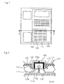
Fig. 1 A plan view showing a button lighting structure included in a telephone related to the present invention. -
Fig. 2 A sectional view showing the button lighting structure included in the telephone related to the present invention. -
Fig. 3 A plan view showing a button lighting structure included in a telephone according to an embodiment. -
Fig. 4 A sectional view showing the button lighting structure included in the telephone according to the embodiment. -
Fig. 5 A perspective view showing, from the outside, a dial cover included in the button lighting structure according to the embodiment. -
Fig. 6 A perspective view showing, from the inside, the dial cover included in the button lighting structure according to the embodiment. - Hereinafter, the specific embodiments of the present invention will be described with reference to the drawings.
-
Fig. 3 is a plan view showing a button lighting structure included in a telephone according to an embodiment.Fig. 4 is a sectional view showing the button lighting structure included in the telephone according to the embodiment.Fig. 5 is a perspective view showing, from the outside, a button cover member included in the button lighting structure according to the embodiment.Fig. 6 is a perspective view showing, from the inside, the button cover member included in the button lighting structure according to the embodiment. - As shown in
Fig. 3 ,telephone 1 according to the embodiment includesbutton lighting structure 2 having a plurality of button members, andcase 3 in whichbutton lighting structure 2 is disposed. As shown inFigs. 3 and 4 ,button lighting structure 2 includes a plurality ofbutton members 5 arranged in a matrix with intervals, and light-emittingelement 6 disposed in the interval of the plurality ofbutton members 5. - As shown in
Figs. 4 to 6 ,button lighting structure 2 includesbutton cover member 7 including plate-like portion 11 having a plurality ofopenings 14 into which the plurality ofbutton members 5 is inserted,translucent guide 12 that guides the movement ofbutton members 5 pushed into the openings, andperipheral wall portion 13 formed along the outer periphery of plate-like portion 11.Button cover member 7 irregularly reflects, by plate-like portion 11 andperipheral wall portion 13, light from light-emittingelement 6 disposed to face plate-like portion 11. -
Button lighting structure 2 includesrubber contact 17 as a button support member for movably supportingbutton members 5 pushed intoopenings 14 ofbutton cover member 7, andcircuit board 18 in which a switch element (not shown), with whichrubber contact 17 that is pushed bybutton members 5 comes into contact, is disposed. -
Button member 5 includestop surface portion 5a pressed by a finger, and side wall portion 5b integrally formed aroundtop surface 5a.Top surface portion 5a is made of a translucent material so that a display portion such as a numeral or a symbol can be lit. Side wall portion 5b is made of a translucent material, into which light output from light-emittingelement 6 and having passed throughguide 12, is connected to the display portion oftop surface portion 5a. - In this embodiment, as shown in
Fig. 3 , twelvebutton members 5 are arranged in a matrix, which includes three columns and four rows. In the embodiment, four light-emittingelements 6 are respectively arranged between an uppermost row and its adjacent row and are respectively arranged between the lowest row and its adjacent row, and unsymmetrically arranged closer toperipheral wall portion 13 side ofbutton cover member 7 than the interval between each column on both sides of and a column in the center. In other words, light-emitting elements 6 are unsymmetrically arranged from the center of the cross intervals among fouradjacent button members 5 toperipheral wall portion 13 side ofbutton cover member 7. - In other words, the arrangement of
button members 5 in this embodiment corresponds to a configuration wherein each of two portions has sixbutton members 5 arranged in a matrix including three columns and two rows, and is arranged up and down. Two light-emittingelements 6 are arranged between the rows, and unsymmetrically from the interval between each column on both sides of and the column in the center to the side ofperipheral wall portion 13. - In the embodiment, six
button members 5 are arranged in the matrix, which includes three columns and two rows. However,button members 5 are not limited to this arrangement. Needless to say, sixbutton members 5 can be arranged in a matrix including two columns and three rows, and two light-emittingelements 6 can be arranged between the columns, and unsymmetrically from the interval between each row on both sides of and the rows in the center in a vertical direction toperipheral wall portion 13 side. This configuration can provide the same effects as th6]
Guide 12 ofbutton cover member 7 is formed along the peripheral edge ofopening 14.Guide 12 includesnotch 19 formed to directly apply the light from light-emittingelement 6 to side wall portion 5b ofbutton member 5, and light from one light-emittingelement 6 can be efficiently entered into fourbutton members 5. - Four light-emitting
elements 6 are arranged at desired positions with respect to twelvebutton members 5, and the light from light-emittingelement 6 is irregularly reflected inbutton cover member 7. Thus, the number of light-emittingelements 6 necessary forlighting button members 5 is reduced, andbutton members 5 are lit to be uniform in luminance. - The LED is used for light-emitting
element 6, and each light-emittingelement 6 is disposed at a predetermined position oncircuit board 18 with respect tobutton member 5 as described above. -
Button cover member 7 is formed by combining a first member including plate-like portion 11 andperipheral wall portion 13 with a secondmember including guide 12. The second member is included in the first member. -
Button cover member 7 is formed by two-color molding which uses , for example, a white resin material for the first member and a transparent resin material for the second member. This enablesbutton cover member 7 to irregularly reflect the light from light-emittingelement 6 effectively by using plate-like portion 11 andside wall portion 13 which were formed into white, thereby efficiently lightingbutton member 5 with the light from light-emittingelement 6. -
Case 3 includesopening 3a in whichbutton cover member 7 is disposed, andtransparent panel member 20 is disposed over plate-like portion 11 ofbutton cover member 7 fitted in opening 3 a andcase 3.Information display sheet 21 is held between plate-like portion 11 ofbutton cover member 7 andpanel member 20.Case 3 andbutton cover member 7 fitted in opening 3a ofcase 3 are arranged onrubber contact 17. - On
circuit board 18, light-emittingelement 6 is located at a position which faces plate-like portion 11 ofbutton cover member 7. In the surface ofcircuit board 18 in whichrubber contact 17 is located, an irregular reflection film (not shown) for irregularly reflecting the light from light-emittingelement 6 is formed. For this irregular reflection film, a white coated film is used. -
Rubber contact 17 made of a translucent resin material is disposed oncircuit board 18. Inrubber contact 17, a plurality ofsupports 17a for supporting the lower ends ofbutton members 5 is formed to be elastically displaced. Each switch element ofcircuit board 18 is disposed directly below eachsupport 17a ofrubber contact 17.Rubber contact 17 hasopening 17b which is formed so that each light-emittingelement 6 oncircuit board 18 can face plate-like portion 11 ofbutton cover member 7. - The state of lighting the plurality of
button members 5 arranged in the matrix inbutton lighting structure 2 included intelephone 1 thus configured will be described. - In
button lighting structure 2, as shown inFig. 4 , a part of the light emitted from light-emittingelement 6 passes throughguide 2 or side wall portion 5b ofbutton member 5, and reachestop surface portion 5a ofbutton member 5 tolight button member 5. - The light emitted from light-emitting
element 6 to plate-like portion 11 ofbutton cover member 7 is irregularly reflected by plate-like portion 11, transmitted throughguide 12 andsupport 17a ofrubber contact 17, and irregularly reflected by the irregular reflection film formed in one surface ofcircuit board 18. Then, the light irregularly reflected oncircuit board 18 enters intobutton member 5, and reachestop surface portion 5a ofbutton member 5 to light it. - The light emitted from light-emitting
element 6 to support 17a ofbutton cover member 7 passes throughsupport 17a to be applied to peripheral 1wall portion 13 ofbutton cover member 7. The light applied toperipheral wall portion 13 is irregularly reflected byperipheral wall portion 13, transmitted throughguide 12 and side wall portion 5b ofbutton member 5, and then reachestop surface portion 5a ofbutton member 5 to light it. - Further, a part of the light from light-emitting
element 6 is transmitted throughnotch 19 ofbutton cover member 7, and is directly applied tobutton member 5 to lighttop surface portion 5a ofbutton member 5. - Thus, as shown in
Fig. 3 , the light from one light-emittingelement 6 is irregularly reflected by the inner surface ofbutton cover member 7, thereby efficiently lighting fouradjacent button members 5 arranged around one light-emittingelement 6. In this embodiment, twelvebutton members 5 are uniformly lit, by lights from four light-emittingelements 6. - As described above,
button lighting structure 2 of the embodiment includesbutton cover member 7 which has plate-like portion 11 for irregularly reflecting the light from light-emittingelement 6, andperipheral wall portion 13. Thus, the light from light-emittingelement 6 can be irregularly reflected efficiently inbutton cover member 7 to enter intobutton member 5. As a result, according to the embodiment, the light from light-emittingelement 6 can be efficiently used bybutton cover member 7 which has a relatively simple configuration. According to the embodiment, since light-emittingelement 6 is unsymmetrically disposed closer toperipheral wall portion 13 side than the center of the cross interval of fouradjacent button members 5,button members 5 can be lit with uniform luminance. - Thus, according to this embodiment, the number of light-emitting
elements 6 necessary for lighting the plurality ofbutton members 5, which are arranged in the matrix, can be greatly reduced, and the luminance ofbutton members 5 can be made uniform. - Further, according to this embodiment, since the light from light-emitting
element 6 is reflected only inbutton cover member 7,button members 5 can be lit uniformly irrespective of the color ofcase 3. As a result, there is no need to adjust the current value supplied to light-emittingelement 6 according to the color ofcase 3, and the manufacturing process of the telephone, in whichcase 3 of a plurality of colors is used, can be simplified. - The button lighting structure of the present invention is applied to the operation panel of the telephone. Not limited to the telephone, however, the button lighting structure can be suitably used for various buttons included in other electronic devices such as an electronic computer, a keyboard, or a numerical keypad.
- The embodiments of the present invention have been described. However, the present invention is not limited to the embodiments. Various changes understandable to those skilled in the art can be made to the configuration and the specifics of the present invention without departing from the scope of the invention.
- This application claims priority from Japanese Patent Application No.
2010-240860 filed October 27, 2010 -
1 Telephone 2 Button lighting structure 5 Button member 5b Side wall portion 6 Light-emitting element 7 Button cover member 11 Plate- like portion 12 Guide 13 Peripheral wall portion 14 Opening
Claims (7)
- A button lighting structure comprising:a plurality of button members arranged in a matrix with intervals;a light-emitting element disposed in the interval of the plurality of button members; anda button cover member that includes a plate-like portion which has a plurality of openings into which the plurality of button members is inserted, a translucent guide that guides movement of the button members pushed into the openings, and a peripheral wall portion formed along the outer periphery of the plate-like portion, and that is configured to irregularly reflect, by the plate-like portion and the peripheral wall portion, light from the light-emitting element disposed to face the plate-like portion,wherein the button member includes a translucent sidewall portion into which the light, that is emitted from the light-emitting element and that has passed through the guide, enters.
- The button lighting structure according to claim 1, further comprising:a translucent button support member for movably supporting the button members which are pushed into the openings; anda circuit board in which the light-emitting element and a switch element, with which the button support member that is pushed by the button member comes into contact, are arranged, wherein:the button support member is disposed on the circuit board; andan irregular reflection film for irregularly reflecting the light from the light-emitting element is formed on a surface of the circuit board in which the button support member is disposed.
- The button lighting structure according to claim 1 or 2, wherein the light-emitting element is disposed unsymmetrically from a center of a cross interval of the four button members adjacent to each other to the peripheral wall portion side.
- The button lighting structure according to claim 1 or 2, wherein:the six button members are arranged in the matrix including three columns and two rows; andthe two light-emitting elements are arranged between the rows and unsymmetrically from intervals between the columns on both sides of and the column in the center to the side of peripheral wall portion.
- The button lighting structure according to any one of claims 1 to 4, wherein the button cover member is formed by combining a first member having the plate-like portion and the peripheral wall portion with a second member having the guide.
- The button lighting structure according to claim 5, wherein the button cover member is formed by two-color molding using a white resin material for the first member and a transparent resin material for the second member.
- An electronic device comprising:the button lighting structure according to any one of claims 1 to 6; andand a case having an opening in which the button cover member is disposed.
Applications Claiming Priority (2)
| Application Number | Priority Date | Filing Date | Title |
|---|---|---|---|
| JP2010240860A JP4779169B1 (en) | 2010-10-27 | 2010-10-27 | Button lighting structure, electronic equipment |
| PCT/JP2011/056365 WO2012056742A1 (en) | 2010-10-27 | 2011-03-17 | Button lighting structure and electronic device |
Publications (3)
| Publication Number | Publication Date |
|---|---|
| EP2605258A1 true EP2605258A1 (en) | 2013-06-19 |
| EP2605258A4 EP2605258A4 (en) | 2014-04-02 |
| EP2605258B1 EP2605258B1 (en) | 2015-07-22 |
Family
ID=44798080
Family Applications (1)
| Application Number | Title | Priority Date | Filing Date |
|---|---|---|---|
| EP11835886.0A Not-in-force EP2605258B1 (en) | 2010-10-27 | 2011-03-17 | Button lighting structure and electronic device |
Country Status (7)
| Country | Link |
|---|---|
| US (1) | US8803015B2 (en) |
| EP (1) | EP2605258B1 (en) |
| JP (1) | JP4779169B1 (en) |
| CN (1) | CN103069525B (en) |
| AU (1) | AU2011321871B2 (en) |
| CA (1) | CA2809933C (en) |
| WO (1) | WO2012056742A1 (en) |
Families Citing this family (7)
| Publication number | Priority date | Publication date | Assignee | Title |
|---|---|---|---|---|
| TWM448728U (en) * | 2012-10-26 | 2013-03-11 | Darfon Electronics Corp | Backlight module and keyboard |
| JP6102665B2 (en) * | 2013-09-30 | 2017-03-29 | オムロン株式会社 | Operation unit and game machine |
| JP6403208B2 (en) * | 2015-02-03 | 2018-10-10 | アルプス電気株式会社 | Touchpad device |
| FR3064868B1 (en) * | 2017-03-31 | 2019-06-21 | Ingenico Group | COVER OF AN ELECTRONIC PAYMENT TERMINAL, CORRESPONDING ELECTRONIC PAYMENT TERMINAL. |
| US10515508B2 (en) | 2017-09-14 | 2019-12-24 | Ags Llc | Push-buttons for gaming machines |
| JP6858803B2 (en) * | 2019-03-04 | 2021-04-14 | Necパーソナルコンピュータ株式会社 | Keyboard device manufacturing method and electronic device manufacturing method |
| JP7595472B2 (en) | 2021-01-25 | 2024-12-06 | アイホン株式会社 | Intercom Equipment |
Family Cites Families (16)
| Publication number | Priority date | Publication date | Assignee | Title |
|---|---|---|---|---|
| DE3734223A1 (en) * | 1987-10-09 | 1989-04-20 | Boehringer Ingelheim Kg | IMPLANTABLE, BIODEGRADABLE ACTIVE SUBSTANCE RELEASE SYSTEM |
| JPH02117U (en) * | 1988-06-13 | 1990-01-05 | ||
| JPH02155136A (en) * | 1988-12-07 | 1990-06-14 | Matsushita Electric Ind Co Ltd | illuminated pushbutton switch |
| JP2804659B2 (en) | 1991-11-29 | 1998-09-30 | シャープ株式会社 | Telephone push button structure |
| JPH0955143A (en) | 1995-08-15 | 1997-02-25 | Saitama Nippon Denki Kk | Key back light lighting effect device |
| JP2000268664A (en) | 1999-03-19 | 2000-09-29 | Aiphone Co Ltd | Luminous display structure of push-button switch |
| JP4008640B2 (en) | 2000-01-11 | 2007-11-14 | ローム株式会社 | Image reading device |
| JP2005063887A (en) * | 2003-08-19 | 2005-03-10 | Fujitsu Ltd | Key lighting structure |
| JP4378189B2 (en) | 2004-02-24 | 2009-12-02 | 株式会社ケンウッド | Push button device |
| JP4523421B2 (en) * | 2005-01-07 | 2010-08-11 | リンナイ株式会社 | Light emitting device |
| JP4708892B2 (en) * | 2005-07-14 | 2011-06-22 | ポリマテック株式会社 | Illumination device |
| DE112007000420T5 (en) * | 2006-02-20 | 2009-01-02 | Citizen Electronics Co., Ltd., Fujiyoshida-shi | Side surface light emission unit and lighting panel |
| JP2008269864A (en) * | 2007-04-18 | 2008-11-06 | Sunarrow Ltd | Metal dome sheet with push projection and push button switch |
| JP2009139762A (en) * | 2007-12-07 | 2009-06-25 | Fuji Electric Fa Components & Systems Co Ltd | Illuminated display |
| JP2010240860A (en) | 2009-04-01 | 2010-10-28 | Nippon Paper Industries Co Ltd | Thermal recording medium |
| US9082566B2 (en) * | 2010-09-02 | 2015-07-14 | Blackberry Limited | Backlighting assembly for a keypad |
-
2010
- 2010-10-27 JP JP2010240860A patent/JP4779169B1/en active Active
-
2011
- 2011-03-17 CA CA2809933A patent/CA2809933C/en active Active
- 2011-03-17 CN CN201180042313.8A patent/CN103069525B/en not_active Expired - Fee Related
- 2011-03-17 AU AU2011321871A patent/AU2011321871B2/en not_active Ceased
- 2011-03-17 US US13/818,384 patent/US8803015B2/en active Active
- 2011-03-17 EP EP11835886.0A patent/EP2605258B1/en not_active Not-in-force
- 2011-03-17 WO PCT/JP2011/056365 patent/WO2012056742A1/en not_active Ceased
Non-Patent Citations (2)
| Title |
|---|
| No further relevant documents disclosed * |
| See also references of WO2012056742A1 * |
Also Published As
| Publication number | Publication date |
|---|---|
| AU2011321871B2 (en) | 2013-05-23 |
| EP2605258B1 (en) | 2015-07-22 |
| US20130153387A1 (en) | 2013-06-20 |
| WO2012056742A1 (en) | 2012-05-03 |
| JP2012094379A (en) | 2012-05-17 |
| AU2011321871A1 (en) | 2013-03-07 |
| JP4779169B1 (en) | 2011-09-28 |
| CA2809933A1 (en) | 2012-05-03 |
| EP2605258A4 (en) | 2014-04-02 |
| CN103069525B (en) | 2015-04-01 |
| CN103069525A (en) | 2013-04-24 |
| HK1180834A1 (en) | 2013-10-25 |
| CA2809933C (en) | 2014-06-10 |
| US8803015B2 (en) | 2014-08-12 |
Similar Documents
| Publication | Publication Date | Title |
|---|---|---|
| EP2605258B1 (en) | Button lighting structure and electronic device | |
| US7690803B2 (en) | Light emitting sheet module | |
| US7253369B2 (en) | Backlight button assemblage | |
| JP4367850B2 (en) | Illuminated switch | |
| CN201927524U (en) | Multiple-color light-emitting key and multiple-color light-emitting keyboard | |
| US8168905B2 (en) | Lighting keyboard | |
| KR100651413B1 (en) | Key pad assembly | |
| US20080151526A1 (en) | Sheet switch module | |
| KR20080024012A (en) | Keypad Assembly and Mobile Terminal Having Same | |
| CN105911631A (en) | Light guide and light emitting device | |
| CN108447724A (en) | illuminated keyboard | |
| WO2011125359A1 (en) | Led backlight | |
| US10497522B2 (en) | Luminous keyboard | |
| JPWO2008072666A1 (en) | Illuminated input device | |
| US10629394B2 (en) | Keyswitch assembly and keyboard | |
| US10199187B2 (en) | Luminous keyboard | |
| CN102192479B (en) | Light guide sheet, sheet with contact spring and switching device | |
| HK1180834B (en) | Button lighting structure and electronic device | |
| JP2003151392A (en) | Light guide plate with keyboard light emission function | |
| TWM469606U (en) | Back light apparatus used in light-emitting keyboard | |
| JP2011222379A (en) | Light guide sheet, sheet with contact spring, and switch device | |
| KR100940045B1 (en) | Keyboard-type input device for mobile phone and printed circuit board suitable for this | |
| JP2010049812A (en) | Key switch structure | |
| WO2008082127A1 (en) | Printing type lighting guide sheet for light source | |
| KR20100040355A (en) | Back lighting apparatus for keypad assembly |
Legal Events
| Date | Code | Title | Description |
|---|---|---|---|
| PUAI | Public reference made under article 153(3) epc to a published international application that has entered the european phase |
Free format text: ORIGINAL CODE: 0009012 |
|
| 17P | Request for examination filed |
Effective date: 20130313 |
|
| AK | Designated contracting states |
Kind code of ref document: A1 Designated state(s): AL AT BE BG CH CY CZ DE DK EE ES FI FR GB GR HR HU IE IS IT LI LT LU LV MC MK MT NL NO PL PT RO RS SE SI SK SM TR |
|
| DAX | Request for extension of the european patent (deleted) | ||
| A4 | Supplementary search report drawn up and despatched |
Effective date: 20140228 |
|
| RIC1 | Information provided on ipc code assigned before grant |
Ipc: H01H 9/18 20060101ALI20140224BHEP Ipc: H01H 13/02 20060101AFI20140224BHEP Ipc: H04M 1/22 20060101ALI20140224BHEP Ipc: H01H 13/702 20060101ALI20140224BHEP Ipc: H01H 13/83 20060101ALI20140224BHEP |
|
| GRAP | Despatch of communication of intention to grant a patent |
Free format text: ORIGINAL CODE: EPIDOSNIGR1 |
|
| RAP1 | Party data changed (applicant data changed or rights of an application transferred) |
Owner name: NEC PLATFORMS, LTD. |
|
| INTG | Intention to grant announced |
Effective date: 20150401 |
|
| GRAS | Grant fee paid |
Free format text: ORIGINAL CODE: EPIDOSNIGR3 |
|
| GRAA | (expected) grant |
Free format text: ORIGINAL CODE: 0009210 |
|
| AK | Designated contracting states |
Kind code of ref document: B1 Designated state(s): AL AT BE BG CH CY CZ DE DK EE ES FI FR GB GR HR HU IE IS IT LI LT LU LV MC MK MT NL NO PL PT RO RS SE SI SK SM TR |
|
| REG | Reference to a national code |
Ref country code: GB Ref legal event code: FG4D |
|
| REG | Reference to a national code |
Ref country code: CH Ref legal event code: EP |
|
| REG | Reference to a national code |
Ref country code: IE Ref legal event code: FG4D |
|
| REG | Reference to a national code |
Ref country code: AT Ref legal event code: REF Ref document number: 738314 Country of ref document: AT Kind code of ref document: T Effective date: 20150815 |
|
| REG | Reference to a national code |
Ref country code: DE Ref legal event code: R096 Ref document number: 602011018113 Country of ref document: DE |
|
| REG | Reference to a national code |
Ref country code: AT Ref legal event code: MK05 Ref document number: 738314 Country of ref document: AT Kind code of ref document: T Effective date: 20150722 |
|
| REG | Reference to a national code |
Ref country code: LT Ref legal event code: MG4D |
|
| REG | Reference to a national code |
Ref country code: NL Ref legal event code: MP Effective date: 20150722 |
|
| PG25 | Lapsed in a contracting state [announced via postgrant information from national office to epo] |
Ref country code: GR Free format text: LAPSE BECAUSE OF FAILURE TO SUBMIT A TRANSLATION OF THE DESCRIPTION OR TO PAY THE FEE WITHIN THE PRESCRIBED TIME-LIMIT Effective date: 20151023 Ref country code: LT Free format text: LAPSE BECAUSE OF FAILURE TO SUBMIT A TRANSLATION OF THE DESCRIPTION OR TO PAY THE FEE WITHIN THE PRESCRIBED TIME-LIMIT Effective date: 20150722 Ref country code: FI Free format text: LAPSE BECAUSE OF FAILURE TO SUBMIT A TRANSLATION OF THE DESCRIPTION OR TO PAY THE FEE WITHIN THE PRESCRIBED TIME-LIMIT Effective date: 20150722 Ref country code: LV Free format text: LAPSE BECAUSE OF FAILURE TO SUBMIT A TRANSLATION OF THE DESCRIPTION OR TO PAY THE FEE WITHIN THE PRESCRIBED TIME-LIMIT Effective date: 20150722 Ref country code: NO Free format text: LAPSE BECAUSE OF FAILURE TO SUBMIT A TRANSLATION OF THE DESCRIPTION OR TO PAY THE FEE WITHIN THE PRESCRIBED TIME-LIMIT Effective date: 20151022 |
|
| REG | Reference to a national code |
Ref country code: FR Ref legal event code: PLFP Year of fee payment: 6 |
|
| PG25 | Lapsed in a contracting state [announced via postgrant information from national office to epo] |
Ref country code: RS Free format text: LAPSE BECAUSE OF FAILURE TO SUBMIT A TRANSLATION OF THE DESCRIPTION OR TO PAY THE FEE WITHIN THE PRESCRIBED TIME-LIMIT Effective date: 20150722 Ref country code: PL Free format text: LAPSE BECAUSE OF FAILURE TO SUBMIT A TRANSLATION OF THE DESCRIPTION OR TO PAY THE FEE WITHIN THE PRESCRIBED TIME-LIMIT Effective date: 20150722 Ref country code: HR Free format text: LAPSE BECAUSE OF FAILURE TO SUBMIT A TRANSLATION OF THE DESCRIPTION OR TO PAY THE FEE WITHIN THE PRESCRIBED TIME-LIMIT Effective date: 20150722 Ref country code: SE Free format text: LAPSE BECAUSE OF FAILURE TO SUBMIT A TRANSLATION OF THE DESCRIPTION OR TO PAY THE FEE WITHIN THE PRESCRIBED TIME-LIMIT Effective date: 20150722 Ref country code: AT Free format text: LAPSE BECAUSE OF FAILURE TO SUBMIT A TRANSLATION OF THE DESCRIPTION OR TO PAY THE FEE WITHIN THE PRESCRIBED TIME-LIMIT Effective date: 20150722 Ref country code: IS Free format text: LAPSE BECAUSE OF FAILURE TO SUBMIT A TRANSLATION OF THE DESCRIPTION OR TO PAY THE FEE WITHIN THE PRESCRIBED TIME-LIMIT Effective date: 20151122 Ref country code: PT Free format text: LAPSE BECAUSE OF FAILURE TO SUBMIT A TRANSLATION OF THE DESCRIPTION OR TO PAY THE FEE WITHIN THE PRESCRIBED TIME-LIMIT Effective date: 20151123 Ref country code: ES Free format text: LAPSE BECAUSE OF FAILURE TO SUBMIT A TRANSLATION OF THE DESCRIPTION OR TO PAY THE FEE WITHIN THE PRESCRIBED TIME-LIMIT Effective date: 20150722 |
|
| REG | Reference to a national code |
Ref country code: DE Ref legal event code: R097 Ref document number: 602011018113 Country of ref document: DE |
|
| PG25 | Lapsed in a contracting state [announced via postgrant information from national office to epo] |
Ref country code: EE Free format text: LAPSE BECAUSE OF FAILURE TO SUBMIT A TRANSLATION OF THE DESCRIPTION OR TO PAY THE FEE WITHIN THE PRESCRIBED TIME-LIMIT Effective date: 20150722 Ref country code: SK Free format text: LAPSE BECAUSE OF FAILURE TO SUBMIT A TRANSLATION OF THE DESCRIPTION OR TO PAY THE FEE WITHIN THE PRESCRIBED TIME-LIMIT Effective date: 20150722 Ref country code: DK Free format text: LAPSE BECAUSE OF FAILURE TO SUBMIT A TRANSLATION OF THE DESCRIPTION OR TO PAY THE FEE WITHIN THE PRESCRIBED TIME-LIMIT Effective date: 20150722 Ref country code: CZ Free format text: LAPSE BECAUSE OF FAILURE TO SUBMIT A TRANSLATION OF THE DESCRIPTION OR TO PAY THE FEE WITHIN THE PRESCRIBED TIME-LIMIT Effective date: 20150722 Ref country code: IT Free format text: LAPSE BECAUSE OF FAILURE TO SUBMIT A TRANSLATION OF THE DESCRIPTION OR TO PAY THE FEE WITHIN THE PRESCRIBED TIME-LIMIT Effective date: 20150722 |
|
| PLBE | No opposition filed within time limit |
Free format text: ORIGINAL CODE: 0009261 |
|
| STAA | Information on the status of an ep patent application or granted ep patent |
Free format text: STATUS: NO OPPOSITION FILED WITHIN TIME LIMIT |
|
| PG25 | Lapsed in a contracting state [announced via postgrant information from national office to epo] |
Ref country code: RO Free format text: LAPSE BECAUSE OF FAILURE TO SUBMIT A TRANSLATION OF THE DESCRIPTION OR TO PAY THE FEE WITHIN THE PRESCRIBED TIME-LIMIT Effective date: 20150722 |
|
| 26N | No opposition filed |
Effective date: 20160425 |
|
| PG25 | Lapsed in a contracting state [announced via postgrant information from national office to epo] |
Ref country code: BE Free format text: LAPSE BECAUSE OF NON-PAYMENT OF DUE FEES Effective date: 20160331 Ref country code: SI Free format text: LAPSE BECAUSE OF FAILURE TO SUBMIT A TRANSLATION OF THE DESCRIPTION OR TO PAY THE FEE WITHIN THE PRESCRIBED TIME-LIMIT Effective date: 20150722 |
|
| PG25 | Lapsed in a contracting state [announced via postgrant information from national office to epo] |
Ref country code: LU Free format text: LAPSE BECAUSE OF FAILURE TO SUBMIT A TRANSLATION OF THE DESCRIPTION OR TO PAY THE FEE WITHIN THE PRESCRIBED TIME-LIMIT Effective date: 20160317 Ref country code: MC Free format text: LAPSE BECAUSE OF FAILURE TO SUBMIT A TRANSLATION OF THE DESCRIPTION OR TO PAY THE FEE WITHIN THE PRESCRIBED TIME-LIMIT Effective date: 20150722 |
|
| REG | Reference to a national code |
Ref country code: CH Ref legal event code: PL |
|
| REG | Reference to a national code |
Ref country code: IE Ref legal event code: MM4A |
|
| PG25 | Lapsed in a contracting state [announced via postgrant information from national office to epo] |
Ref country code: BE Free format text: LAPSE BECAUSE OF FAILURE TO SUBMIT A TRANSLATION OF THE DESCRIPTION OR TO PAY THE FEE WITHIN THE PRESCRIBED TIME-LIMIT Effective date: 20150722 |
|
| PG25 | Lapsed in a contracting state [announced via postgrant information from national office to epo] |
Ref country code: CH Free format text: LAPSE BECAUSE OF NON-PAYMENT OF DUE FEES Effective date: 20160331 Ref country code: LI Free format text: LAPSE BECAUSE OF NON-PAYMENT OF DUE FEES Effective date: 20160331 Ref country code: IE Free format text: LAPSE BECAUSE OF NON-PAYMENT OF DUE FEES Effective date: 20160317 |
|
| REG | Reference to a national code |
Ref country code: FR Ref legal event code: PLFP Year of fee payment: 7 |
|
| PG25 | Lapsed in a contracting state [announced via postgrant information from national office to epo] |
Ref country code: NL Free format text: LAPSE BECAUSE OF FAILURE TO SUBMIT A TRANSLATION OF THE DESCRIPTION OR TO PAY THE FEE WITHIN THE PRESCRIBED TIME-LIMIT Effective date: 20150722 |
|
| PG25 | Lapsed in a contracting state [announced via postgrant information from national office to epo] |
Ref country code: MT Free format text: LAPSE BECAUSE OF FAILURE TO SUBMIT A TRANSLATION OF THE DESCRIPTION OR TO PAY THE FEE WITHIN THE PRESCRIBED TIME-LIMIT Effective date: 20150722 |
|
| REG | Reference to a national code |
Ref country code: FR Ref legal event code: PLFP Year of fee payment: 8 |
|
| PG25 | Lapsed in a contracting state [announced via postgrant information from national office to epo] |
Ref country code: SM Free format text: LAPSE BECAUSE OF FAILURE TO SUBMIT A TRANSLATION OF THE DESCRIPTION OR TO PAY THE FEE WITHIN THE PRESCRIBED TIME-LIMIT Effective date: 20150722 Ref country code: HU Free format text: LAPSE BECAUSE OF FAILURE TO SUBMIT A TRANSLATION OF THE DESCRIPTION OR TO PAY THE FEE WITHIN THE PRESCRIBED TIME-LIMIT; INVALID AB INITIO Effective date: 20110317 Ref country code: CY Free format text: LAPSE BECAUSE OF FAILURE TO SUBMIT A TRANSLATION OF THE DESCRIPTION OR TO PAY THE FEE WITHIN THE PRESCRIBED TIME-LIMIT Effective date: 20150722 |
|
| PG25 | Lapsed in a contracting state [announced via postgrant information from national office to epo] |
Ref country code: TR Free format text: LAPSE BECAUSE OF FAILURE TO SUBMIT A TRANSLATION OF THE DESCRIPTION OR TO PAY THE FEE WITHIN THE PRESCRIBED TIME-LIMIT Effective date: 20150722 Ref country code: MT Free format text: LAPSE BECAUSE OF FAILURE TO SUBMIT A TRANSLATION OF THE DESCRIPTION OR TO PAY THE FEE WITHIN THE PRESCRIBED TIME-LIMIT Effective date: 20160331 Ref country code: MK Free format text: LAPSE BECAUSE OF FAILURE TO SUBMIT A TRANSLATION OF THE DESCRIPTION OR TO PAY THE FEE WITHIN THE PRESCRIBED TIME-LIMIT Effective date: 20150722 |
|
| PG25 | Lapsed in a contracting state [announced via postgrant information from national office to epo] |
Ref country code: BG Free format text: LAPSE BECAUSE OF FAILURE TO SUBMIT A TRANSLATION OF THE DESCRIPTION OR TO PAY THE FEE WITHIN THE PRESCRIBED TIME-LIMIT Effective date: 20150722 |
|
| PG25 | Lapsed in a contracting state [announced via postgrant information from national office to epo] |
Ref country code: AL Free format text: LAPSE BECAUSE OF FAILURE TO SUBMIT A TRANSLATION OF THE DESCRIPTION OR TO PAY THE FEE WITHIN THE PRESCRIBED TIME-LIMIT Effective date: 20150722 |
|
| PGFP | Annual fee paid to national office [announced via postgrant information from national office to epo] |
Ref country code: GB Payment date: 20220321 Year of fee payment: 12 Ref country code: DE Payment date: 20220322 Year of fee payment: 12 |
|
| PGFP | Annual fee paid to national office [announced via postgrant information from national office to epo] |
Ref country code: FR Payment date: 20220322 Year of fee payment: 12 |
|
| REG | Reference to a national code |
Ref country code: DE Ref legal event code: R119 Ref document number: 602011018113 Country of ref document: DE |
|
| GBPC | Gb: european patent ceased through non-payment of renewal fee |
Effective date: 20230317 |
|
| PG25 | Lapsed in a contracting state [announced via postgrant information from national office to epo] |
Ref country code: GB Free format text: LAPSE BECAUSE OF NON-PAYMENT OF DUE FEES Effective date: 20230317 |
|
| PG25 | Lapsed in a contracting state [announced via postgrant information from national office to epo] |
Ref country code: GB Free format text: LAPSE BECAUSE OF NON-PAYMENT OF DUE FEES Effective date: 20230317 Ref country code: FR Free format text: LAPSE BECAUSE OF NON-PAYMENT OF DUE FEES Effective date: 20230331 Ref country code: DE Free format text: LAPSE BECAUSE OF NON-PAYMENT OF DUE FEES Effective date: 20231003 |