EP2604729A1 - Method for manufacturing a silicon carbide wafer and respective equipment - Google Patents
Method for manufacturing a silicon carbide wafer and respective equipment Download PDFInfo
- Publication number
- EP2604729A1 EP2604729A1 EP12195884.7A EP12195884A EP2604729A1 EP 2604729 A1 EP2604729 A1 EP 2604729A1 EP 12195884 A EP12195884 A EP 12195884A EP 2604729 A1 EP2604729 A1 EP 2604729A1
- Authority
- EP
- European Patent Office
- Prior art keywords
- layer
- susceptor
- reaction chamber
- wafer
- substrate
- Prior art date
- Legal status (The legal status is an assumption and is not a legal conclusion. Google has not performed a legal analysis and makes no representation as to the accuracy of the status listed.)
- Withdrawn
Links
Images




Classifications
-
- C—CHEMISTRY; METALLURGY
- C30—CRYSTAL GROWTH
- C30B—SINGLE-CRYSTAL GROWTH; UNIDIRECTIONAL SOLIDIFICATION OF EUTECTIC MATERIAL OR UNIDIRECTIONAL DEMIXING OF EUTECTOID MATERIAL; REFINING BY ZONE-MELTING OF MATERIAL; PRODUCTION OF A HOMOGENEOUS POLYCRYSTALLINE MATERIAL WITH DEFINED STRUCTURE; SINGLE CRYSTALS OR HOMOGENEOUS POLYCRYSTALLINE MATERIAL WITH DEFINED STRUCTURE; AFTER-TREATMENT OF SINGLE CRYSTALS OR A HOMOGENEOUS POLYCRYSTALLINE MATERIAL WITH DEFINED STRUCTURE; APPARATUS THEREFOR
- C30B9/00—Single-crystal growth from melt solutions using molten solvents
- C30B9/04—Single-crystal growth from melt solutions using molten solvents by cooling of the solution
- C30B9/06—Single-crystal growth from melt solutions using molten solvents by cooling of the solution using as solvent a component of the crystal composition
-
- H—ELECTRICITY
- H10—SEMICONDUCTOR DEVICES; ELECTRIC SOLID-STATE DEVICES NOT OTHERWISE PROVIDED FOR
- H10P—GENERIC PROCESSES OR APPARATUS FOR THE MANUFACTURE OR TREATMENT OF DEVICES COVERED BY CLASS H10
- H10P95/00—Generic processes or apparatus for manufacture or treatments not covered by the other groups of this subclass
- H10P95/11—Separation of active layers from substrates
-
- C—CHEMISTRY; METALLURGY
- C23—COATING METALLIC MATERIAL; COATING MATERIAL WITH METALLIC MATERIAL; CHEMICAL SURFACE TREATMENT; DIFFUSION TREATMENT OF METALLIC MATERIAL; COATING BY VACUUM EVAPORATION, BY SPUTTERING, BY ION IMPLANTATION OR BY CHEMICAL VAPOUR DEPOSITION, IN GENERAL; INHIBITING CORROSION OF METALLIC MATERIAL OR INCRUSTATION IN GENERAL
- C23C—COATING METALLIC MATERIAL; COATING MATERIAL WITH METALLIC MATERIAL; SURFACE TREATMENT OF METALLIC MATERIAL BY DIFFUSION INTO THE SURFACE, BY CHEMICAL CONVERSION OR SUBSTITUTION; COATING BY VACUUM EVAPORATION, BY SPUTTERING, BY ION IMPLANTATION OR BY CHEMICAL VAPOUR DEPOSITION, IN GENERAL
- C23C16/00—Chemical coating by decomposition of gaseous compounds, without leaving reaction products of surface material in the coating, i.e. chemical vapour deposition [CVD] processes
- C23C16/01—Chemical coating by decomposition of gaseous compounds, without leaving reaction products of surface material in the coating, i.e. chemical vapour deposition [CVD] processes on temporary substrates, e.g. substrates subsequently removed by etching
-
- C—CHEMISTRY; METALLURGY
- C23—COATING METALLIC MATERIAL; COATING MATERIAL WITH METALLIC MATERIAL; CHEMICAL SURFACE TREATMENT; DIFFUSION TREATMENT OF METALLIC MATERIAL; COATING BY VACUUM EVAPORATION, BY SPUTTERING, BY ION IMPLANTATION OR BY CHEMICAL VAPOUR DEPOSITION, IN GENERAL; INHIBITING CORROSION OF METALLIC MATERIAL OR INCRUSTATION IN GENERAL
- C23C—COATING METALLIC MATERIAL; COATING MATERIAL WITH METALLIC MATERIAL; SURFACE TREATMENT OF METALLIC MATERIAL BY DIFFUSION INTO THE SURFACE, BY CHEMICAL CONVERSION OR SUBSTITUTION; COATING BY VACUUM EVAPORATION, BY SPUTTERING, BY ION IMPLANTATION OR BY CHEMICAL VAPOUR DEPOSITION, IN GENERAL
- C23C16/00—Chemical coating by decomposition of gaseous compounds, without leaving reaction products of surface material in the coating, i.e. chemical vapour deposition [CVD] processes
- C23C16/02—Pretreatment of the material to be coated
- C23C16/0209—Pretreatment of the material to be coated by heating
- C23C16/0218—Pretreatment of the material to be coated by heating in a reactive atmosphere
-
- C—CHEMISTRY; METALLURGY
- C23—COATING METALLIC MATERIAL; COATING MATERIAL WITH METALLIC MATERIAL; CHEMICAL SURFACE TREATMENT; DIFFUSION TREATMENT OF METALLIC MATERIAL; COATING BY VACUUM EVAPORATION, BY SPUTTERING, BY ION IMPLANTATION OR BY CHEMICAL VAPOUR DEPOSITION, IN GENERAL; INHIBITING CORROSION OF METALLIC MATERIAL OR INCRUSTATION IN GENERAL
- C23C—COATING METALLIC MATERIAL; COATING MATERIAL WITH METALLIC MATERIAL; SURFACE TREATMENT OF METALLIC MATERIAL BY DIFFUSION INTO THE SURFACE, BY CHEMICAL CONVERSION OR SUBSTITUTION; COATING BY VACUUM EVAPORATION, BY SPUTTERING, BY ION IMPLANTATION OR BY CHEMICAL VAPOUR DEPOSITION, IN GENERAL
- C23C16/00—Chemical coating by decomposition of gaseous compounds, without leaving reaction products of surface material in the coating, i.e. chemical vapour deposition [CVD] processes
- C23C16/22—Chemical coating by decomposition of gaseous compounds, without leaving reaction products of surface material in the coating, i.e. chemical vapour deposition [CVD] processes characterised by the deposition of inorganic material, other than metallic material
- C23C16/30—Deposition of compounds, mixtures or solid solutions, e.g. borides, carbides, nitrides
- C23C16/32—Carbides
- C23C16/325—Silicon carbide
-
- C—CHEMISTRY; METALLURGY
- C23—COATING METALLIC MATERIAL; COATING MATERIAL WITH METALLIC MATERIAL; CHEMICAL SURFACE TREATMENT; DIFFUSION TREATMENT OF METALLIC MATERIAL; COATING BY VACUUM EVAPORATION, BY SPUTTERING, BY ION IMPLANTATION OR BY CHEMICAL VAPOUR DEPOSITION, IN GENERAL; INHIBITING CORROSION OF METALLIC MATERIAL OR INCRUSTATION IN GENERAL
- C23C—COATING METALLIC MATERIAL; COATING MATERIAL WITH METALLIC MATERIAL; SURFACE TREATMENT OF METALLIC MATERIAL BY DIFFUSION INTO THE SURFACE, BY CHEMICAL CONVERSION OR SUBSTITUTION; COATING BY VACUUM EVAPORATION, BY SPUTTERING, BY ION IMPLANTATION OR BY CHEMICAL VAPOUR DEPOSITION, IN GENERAL
- C23C16/00—Chemical coating by decomposition of gaseous compounds, without leaving reaction products of surface material in the coating, i.e. chemical vapour deposition [CVD] processes
- C23C16/44—Chemical coating by decomposition of gaseous compounds, without leaving reaction products of surface material in the coating, i.e. chemical vapour deposition [CVD] processes characterised by the method of coating
- C23C16/458—Chemical coating by decomposition of gaseous compounds, without leaving reaction products of surface material in the coating, i.e. chemical vapour deposition [CVD] processes characterised by the method of coating characterised by the method used for supporting substrates in the reaction chamber
- C23C16/4582—Rigid and flat substrates, e.g. plates or discs
- C23C16/4583—Rigid and flat substrates, e.g. plates or discs the substrate being supported substantially horizontally
-
- C—CHEMISTRY; METALLURGY
- C30—CRYSTAL GROWTH
- C30B—SINGLE-CRYSTAL GROWTH; UNIDIRECTIONAL SOLIDIFICATION OF EUTECTIC MATERIAL OR UNIDIRECTIONAL DEMIXING OF EUTECTOID MATERIAL; REFINING BY ZONE-MELTING OF MATERIAL; PRODUCTION OF A HOMOGENEOUS POLYCRYSTALLINE MATERIAL WITH DEFINED STRUCTURE; SINGLE CRYSTALS OR HOMOGENEOUS POLYCRYSTALLINE MATERIAL WITH DEFINED STRUCTURE; AFTER-TREATMENT OF SINGLE CRYSTALS OR A HOMOGENEOUS POLYCRYSTALLINE MATERIAL WITH DEFINED STRUCTURE; APPARATUS THEREFOR
- C30B19/00—Liquid-phase epitaxial-layer growth
- C30B19/02—Liquid-phase epitaxial-layer growth using molten solvents, e.g. flux
- C30B19/04—Liquid-phase epitaxial-layer growth using molten solvents, e.g. flux the solvent being a component of the crystal composition
-
- C—CHEMISTRY; METALLURGY
- C30—CRYSTAL GROWTH
- C30B—SINGLE-CRYSTAL GROWTH; UNIDIRECTIONAL SOLIDIFICATION OF EUTECTIC MATERIAL OR UNIDIRECTIONAL DEMIXING OF EUTECTOID MATERIAL; REFINING BY ZONE-MELTING OF MATERIAL; PRODUCTION OF A HOMOGENEOUS POLYCRYSTALLINE MATERIAL WITH DEFINED STRUCTURE; SINGLE CRYSTALS OR HOMOGENEOUS POLYCRYSTALLINE MATERIAL WITH DEFINED STRUCTURE; AFTER-TREATMENT OF SINGLE CRYSTALS OR A HOMOGENEOUS POLYCRYSTALLINE MATERIAL WITH DEFINED STRUCTURE; APPARATUS THEREFOR
- C30B19/00—Liquid-phase epitaxial-layer growth
- C30B19/08—Heating of the reaction chamber or the substrate
-
- C—CHEMISTRY; METALLURGY
- C30—CRYSTAL GROWTH
- C30B—SINGLE-CRYSTAL GROWTH; UNIDIRECTIONAL SOLIDIFICATION OF EUTECTIC MATERIAL OR UNIDIRECTIONAL DEMIXING OF EUTECTOID MATERIAL; REFINING BY ZONE-MELTING OF MATERIAL; PRODUCTION OF A HOMOGENEOUS POLYCRYSTALLINE MATERIAL WITH DEFINED STRUCTURE; SINGLE CRYSTALS OR HOMOGENEOUS POLYCRYSTALLINE MATERIAL WITH DEFINED STRUCTURE; AFTER-TREATMENT OF SINGLE CRYSTALS OR A HOMOGENEOUS POLYCRYSTALLINE MATERIAL WITH DEFINED STRUCTURE; APPARATUS THEREFOR
- C30B19/00—Liquid-phase epitaxial-layer growth
- C30B19/12—Liquid-phase epitaxial-layer growth characterised by the substrate
-
- C—CHEMISTRY; METALLURGY
- C30—CRYSTAL GROWTH
- C30B—SINGLE-CRYSTAL GROWTH; UNIDIRECTIONAL SOLIDIFICATION OF EUTECTIC MATERIAL OR UNIDIRECTIONAL DEMIXING OF EUTECTOID MATERIAL; REFINING BY ZONE-MELTING OF MATERIAL; PRODUCTION OF A HOMOGENEOUS POLYCRYSTALLINE MATERIAL WITH DEFINED STRUCTURE; SINGLE CRYSTALS OR HOMOGENEOUS POLYCRYSTALLINE MATERIAL WITH DEFINED STRUCTURE; AFTER-TREATMENT OF SINGLE CRYSTALS OR A HOMOGENEOUS POLYCRYSTALLINE MATERIAL WITH DEFINED STRUCTURE; APPARATUS THEREFOR
- C30B29/00—Single crystals or homogeneous polycrystalline material with defined structure characterised by the material or by their shape
- C30B29/10—Inorganic compounds or compositions
- C30B29/36—Carbides
-
- C—CHEMISTRY; METALLURGY
- C30—CRYSTAL GROWTH
- C30B—SINGLE-CRYSTAL GROWTH; UNIDIRECTIONAL SOLIDIFICATION OF EUTECTIC MATERIAL OR UNIDIRECTIONAL DEMIXING OF EUTECTOID MATERIAL; REFINING BY ZONE-MELTING OF MATERIAL; PRODUCTION OF A HOMOGENEOUS POLYCRYSTALLINE MATERIAL WITH DEFINED STRUCTURE; SINGLE CRYSTALS OR HOMOGENEOUS POLYCRYSTALLINE MATERIAL WITH DEFINED STRUCTURE; AFTER-TREATMENT OF SINGLE CRYSTALS OR A HOMOGENEOUS POLYCRYSTALLINE MATERIAL WITH DEFINED STRUCTURE; APPARATUS THEREFOR
- C30B33/00—After-treatment of single crystals or homogeneous polycrystalline material with defined structure
-
- C—CHEMISTRY; METALLURGY
- C30—CRYSTAL GROWTH
- C30B—SINGLE-CRYSTAL GROWTH; UNIDIRECTIONAL SOLIDIFICATION OF EUTECTIC MATERIAL OR UNIDIRECTIONAL DEMIXING OF EUTECTOID MATERIAL; REFINING BY ZONE-MELTING OF MATERIAL; PRODUCTION OF A HOMOGENEOUS POLYCRYSTALLINE MATERIAL WITH DEFINED STRUCTURE; SINGLE CRYSTALS OR HOMOGENEOUS POLYCRYSTALLINE MATERIAL WITH DEFINED STRUCTURE; AFTER-TREATMENT OF SINGLE CRYSTALS OR A HOMOGENEOUS POLYCRYSTALLINE MATERIAL WITH DEFINED STRUCTURE; APPARATUS THEREFOR
- C30B33/00—After-treatment of single crystals or homogeneous polycrystalline material with defined structure
- C30B33/06—Joining of crystals
-
- H—ELECTRICITY
- H10—SEMICONDUCTOR DEVICES; ELECTRIC SOLID-STATE DEVICES NOT OTHERWISE PROVIDED FOR
- H10P—GENERIC PROCESSES OR APPARATUS FOR THE MANUFACTURE OR TREATMENT OF DEVICES COVERED BY CLASS H10
- H10P14/00—Formation of materials, e.g. in the shape of layers or pillars
- H10P14/20—Formation of materials, e.g. in the shape of layers or pillars of semiconductor materials
- H10P14/29—Formation of materials, e.g. in the shape of layers or pillars of semiconductor materials characterised by the substrates
- H10P14/2901—Materials
- H10P14/2902—Materials being Group IVA materials
- H10P14/2905—Silicon, silicon germanium or germanium
-
- H—ELECTRICITY
- H10—SEMICONDUCTOR DEVICES; ELECTRIC SOLID-STATE DEVICES NOT OTHERWISE PROVIDED FOR
- H10P—GENERIC PROCESSES OR APPARATUS FOR THE MANUFACTURE OR TREATMENT OF DEVICES COVERED BY CLASS H10
- H10P14/00—Formation of materials, e.g. in the shape of layers or pillars
- H10P14/20—Formation of materials, e.g. in the shape of layers or pillars of semiconductor materials
- H10P14/34—Deposited materials, e.g. layers
- H10P14/3402—Deposited materials, e.g. layers characterised by the chemical composition
- H10P14/3404—Deposited materials, e.g. layers characterised by the chemical composition being Group IVA materials
- H10P14/3408—Silicon carbide
-
- H—ELECTRICITY
- H10—SEMICONDUCTOR DEVICES; ELECTRIC SOLID-STATE DEVICES NOT OTHERWISE PROVIDED FOR
- H10P—GENERIC PROCESSES OR APPARATUS FOR THE MANUFACTURE OR TREATMENT OF DEVICES COVERED BY CLASS H10
- H10P14/00—Formation of materials, e.g. in the shape of layers or pillars
- H10P14/20—Formation of materials, e.g. in the shape of layers or pillars of semiconductor materials
- H10P14/34—Deposited materials, e.g. layers
- H10P14/3466—Crystal orientation
Definitions
- the present invention relates to the electronics sector. More in detail, the present invention relates to a method for manufacturing a semiconductor material wafer.
- a semiconductor electronic device either an Integrated Circuit (IC) or a power device, is a circuit whose components are directly fabricated in a semiconductor material substrate.
- the substrates of the great majority of the ICs presently available on the market are obtained from silicon (Si) wafers.
- silicon carbide (SiC) wafers have been developed. Compared to silicon, silicon carbide has different chemical-physical properties, at least in part due to the different band gap value (indeed, silicon carbide has a band gap higher than that of silicon). For example, silicon carbide is characterized by a breaking voltage higher than that of the silicon, and it is thus an optimal material for manufacturing electronic devices for power applications, since a wafer (and, thus, a substrate for an IC) formed in silicon carbide is capable of managing voltages of relatively high values even with a relatively thin thickness. Moreover, using a silicon carbide wafer is particularly advantageous in all the electronic fields requiring the managing of high frequency signals.
- Silicon wafers are typically formed in pure monocrystalline silicon.
- a known manufacturing process for generating wafers of this type is the so-called “Czochralski growth process", which provides for introducing a monocrystalline silicon seed within a mass of melted silicon, and the gradual extraction of the seed from the melted silicon together with a slow rotation of the seed itself.
- silicon carbide is a material which directly passes (sublimates) from the solid phase to the vapour phase, without passing from any liquid phase, the Czochralski growth process cannot be used, since this latter process just requires that the seed is inserted in a melting of the desired material.
- Silicon carbide may occurs in a number of different chrystallographic structures (polytypes). Among the number of polytypes, the most common are the cubic polytype (3C polytype), the hexagonal polytype (4H and 6H polytypes), and the rhombohedric polytype (15R polytype).
- 3C polytype cubic polytype
- 4H and 6H polytypes hexagonal polytype
- 15R polytype rhombohedric polytype
- a possible solution for the 3C polytype may provide for using epitaxial growth techniques.
- epitaxial growth it is intended a method which provides for the deposition of thin layers of material on a crystalline substrate, which addresses its growing and determinates its structural properties.
- 3C SiC 3C SiC crystal
- some known solutions provides for the growing of a 3C SiC layer by means of a heteroepitaxial process starting from a silicon substrate.
- such known solutions only allow the growing of layers having very thin thickness (lower than a micron) or scarce quality (high defectiveness).
- a possible solution of the drawbacks which affects the presently used growing processes provides for the deposition of a first layer of the desired material on a crystalline substrate having a lower melting temperature, the subsequent elimination of the substrate by means of the melting, and the deposition of a second layer of the desired material on the first layer.
- a first aspect according to an embodiment of the present invention relates to a method for producing a wafer of a first semiconductor material.
- Said first semiconductor material has a first melting temperature.
- the method comprises providing a crystalline substrate of a second semiconductor material having a second melting temperature lower than the first melting temperature, and exposing the crystalline substrate to a flow of first material precursors for forming a first layer of the first material on the substrate.
- the method further comprising bringing the crystalline substrate to a first process temperature higher than the second melting temperature, and at the same time lower than the first melting temperature, in such a way the second material melts, separating the second melted material from the first layer, and exposing the first layer to the flow of the first material precursor for forming a second layer of the first material on the first layer.
- reaction chamber for producing a semiconductor material wafer.
- Such reaction chamber comprises a susceptor, heating means for heating the susceptor, and conduction means for providing a precursors flow.
- Said susceptor comprises a plurality of draining openings adapted to make melted material generated during the manufacturing of the semiconductor material wafer flowing out from the susceptor.
- a further aspect of the present invention relates to a semiconductor material wafer.
- the present detailed description refers to a method for manufacturing a 3C SiC wafer by means of a Chemical Vapor Deposition (CVD) hetero-homo epitaxial growing process starting from a silicon substrate, and to a corresponding reaction chamber wherein carrying out such method.
- CVD Chemical Vapor Deposition
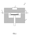
- Figure 1 schematically illustrates by means of a sectional view a reaction chamber 100 wherein the concepts of the present invention may be applied.
- the reaction chamber 100 comprises a hollow body 103 formed in an insulating material, adapted to thermally insulating the inner cavity from the external environment.
- the reaction chamber 100 comprises a support 105 (in jargon, "susceptor") adapted to sustain the crystalline substrate (identified in figure with the reference 102) on which a 3C SiC layer is epitaxially grown, as will be described in detail in the following of the present description.
- the susceptor 105 is a substantially flat element, for example having a circular shape, implemented in a material having a high melting temperature, such as for example naked graphite having a high degree of pureness and a high dilatation coefficient.
- the reaction chamber comprises heating means 110 configured to heat the susceptor 105.
- the heating means 110 may be of the inductive type, comprising coils, or of the resistive type, comprising carbide covered resistors.
- the deposition process provides that the substrate 102, supported and heated by the susceptor 105, is invested by a gas flow that carries - in gaseous form - the particles of the material to be deposited on the substrate 102 itself; in jargon, the gas flow comprising particles of a material to be deposed is identified as "precursor" of the material itself.
- An input duct 115 is provided for inputting the precursors within the reaction chamber 100, and an output duct 120 is provided for discharging the reaction gases outside the reaction chamber 100.
- the input duct 115 and the output duct 120 are arranged in such a way that the precursor flow hits the substrate 102 longitudinally to the main surface of the substrate 102 itself.
- a reaction chamber of this type is in jargon referred to as horizontal flux reaction chamber.
- the concepts of the present invention may be however applied to vertical flux reaction chambers, wherein the input duct and the output duct are arranged in such a way that the precursor flow hits the substrate transversally to the main surface of the substrate itself, and wherein the heating element is of the induction type.
- a possible example of a reaction chamber of this type is illustrated in Figure 2 .
- the method according to an embodiment of the present invention provides that from the wafer in process melted material is generated, which melted material requires to be drained and collected, for being removed in a second time.
- the susceptor is provided with draining openings for the flowing out of the melted material.
- Figure 3A is a view from the above of a susceptor 200 according to an embodiment of the present invention
- Figure 3B is a sectional view of the susceptor 200 of figure 3A taken along a sectional plane perpendicular to the surface of the susceptor 200 and passing from the line II-II.
- the susceptor 200 comprises a plurality of circular draining openings, identified in figure with the reference 205, uniformly arranged along the susceptor surface 205.
- the draining openings are shaped according to a "funnel" shape, with a beginning cone-shaped portion and a terminating cylindrical portion.
- Figure 4A is a view from the above of a susceptor 200' according to a further embodiment of the present invention
- Figure 4B is a sectional view of the susceptor 200' of Figure 4A taken along a sectional plane perpendicular to the surface of the susceptor 200' and passing from the line III-III.
- the susceptor 200' comprises a plurality of draining openings substantially having a slit shape, identified in figure with the reference 305, in such a way to define a substantially grid structure on the surface of the susceptor.
- susceptors 200, 200' illustrated in Figures 3A, 3B , 4A and 4B are to be considered only for exemplificative and non limitative purposes, since the concepts of the present invention may be applied to susceptors having draining openings having different shapes and arrangements ( e.g., having a polygonal shape).
- a susceptor according to the present invention - i.e., provided with draining openings - is located within the reaction chamber 100 on a support comprising a gathering tank 125 (for example, in graphite).
- the employed susceptor is the susceptor 200 of Figures 3A and 3B , provided with circular openings.
- susceptors provided with draining openings having a different shape such as the slit draining openings of the susceptor 200' of Figures 4A and 4B .
- a method for manufacturing a 3C SiC wafer which exploits the reaction chamber 100 (indifferently, at horizontal or vertical flow) equipped with the susceptor 200 provided with draining openings according to an embodiment of the present invention.
- Figure 6 illustrates a possible thermal profile 400 of the reaction chamber 100 during the various phases of the method according to an embodiment of the present invention.
- PHASE 1 The reaction chamber 100 is at the room temperature.
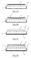
- a silicon crystalline substrate 102 for example of the (100) type, is positioned on the susceptor 200, A situation of this type is shown in Figure 7A .
- the heating means 110 are activated for rising the temperature of the reaction chamber 100 until reaching a temperature equal to about 1000-1100°C.
- the ducts 115 and 120 are opened for immersing the substrate 102 in a hydrogen flow.
- PHASE 3 The temperature is kept at the same value reached in the previous phase.
- the surface of the substrate 102 is subjected to activation operations, for example by means H 2 , HCl and deposition of silicon buffer.
- PHASE 4 The temperature of the reaction chamber 100 is risen until about 1330-1380°C. A carbon precursor is added to the hydrogen flow, in order to carbonise the superficial silicon atoms of the substrate 102, and obtaining a thin layer, of the order of few nanometers, of SiC (in jargon, "ramp carbonisation"). Such thin layer of silicon carbide has the purpose of acting as a seed for the SiC growth which will be carried out in the following phase.
- PHASE 5 Keeping the temperature of the reaction chamber 100 at about 1330-1380°C, a silicon precursor is added to the carbon precursor. In this way, a 3C SiC layer is caused to grow from the thin layer previously generated (epitaxial grow). Since the silicon of the substrate ha a reticule that is different than the silicon carbide of the growing layer (5,43 angstrom for the silicon and 4,36 angstrom for the silicon carbide), the more the 3C Sic layer grows, the more the semiconductor wafer tends to warp.
- the temperature of the reaction chamber 100 is risen until reaching a temperature higher than the melting temperature of the silicon, and at the same time lower than the melting temperature of the 3C SiC.
- the reaction chamber 100 is brought to a temperature of about 1450-1460°C.
- PHASE 7 The reaction chamber 100 is kept at the temperature just reached, while the precursor flow (silicon and carbon) is kept constant with respect to the preceding phases. In this way, while the 3C SiC layer 510 continues to grow in thickness, since supplied by the precursors of the silicon and of the carbon, the underneath silicon substrate 102 starts to melt, and in the melted state passes through the draining openings of the susceptor 200, for being collected in the underneath gathering tank 125. With the melting, and the passage in the underneath gathering tank 125, of an ever increasing portion of the substrate 102, the warping affecting the wafer tends to diminish, being the wafer made up more and more by silicon carbide and less and less by silicon.
- the duration of this phase is set in such a way to allow the melting and the separation of (substantially) all the silicon of the substrate 102.
- the resulting semiconductor material wafer located on the susceptor 200 - globally identified in figure with the reference 515 - results to be solely formed by the 3C SiC layer 510; the silicon collected by the gathering tank 125 after the melting of the substrate 102 is identified in figure with the reference 520.
- the SiC layer 515 results to be planar, It is underlined that growing a 3C SiC layer 510 of sufficiently high thickness (30-40 microns, see PHASE 5) before rising the temperature above the melting point of the silicon results to be very advantageous, since said SiC layer should be capable of remaining integral even without the underneath silicon substrate 102. With a 3C SiC 510 layer too much thin, the wafer 515 would risk to break further to the silicon melting.
- the thickness of the 3C SiC layer 510 continues to grow.
- the temperature of the reaction chamber 100 is brought again to a value lower than the melting temperature of the silicon, for example at about 1370°C. In this way, the melted silicon 520 collected in the gathering tank 125 firms up.
- PHASE 9 Keeping the reaction chamber 100 at the temperature reached in PHASE 8, and continuing to constantly provide the flow of silicon and carbon precursors, a further layer of 3C SiC, identified in Figure 7D with the reference 530, is grown on the layer 510 of SiC, having desired thickness and resistivity. Unlike the preceding phases, wherein the growing was of the heteroepitaxial type - indeed, other than the SiC layer 510 it was present also the silicon substrate 102 -, the growing of the layer 530 results to be of the homoepitaxial type, since the wafer 515 results to be exclusively formed by SiC. During this phase, it is further possible to input in the chamber - together with the silicon and carbon precursors - doping elements for varying the resistivity of the layer 530.
- the portion of the wafer 515 corresponding to the layer 530 may be thus used as an active zone wherein forming the electronic devices.
- PHASE 10 Having reached the desired thickness of the SiC layer, the temperature of the reaction chamber 100 is taken back to the room temperature, and the precursors flow is interrupted.
- a wafer 515 of 3C SiC is obtained as final product, having the desired thickness and resistivity and a good planarity degree, and a mass of polycrystalline silicon as waste product.
- the 3C SiC wafer fabrication method above described may be optimised using a reaction chamber with a mobile gathering tank, adapted to pass in a particular phases of the growing process from a first configuration, wherein the tank is in contact with the susceptor and forms therewith a single body, to a second configuration, wherein the tank and the susceptor are separated, and viceversa.
- Figure 8A is a sectional view of a mobile gathering tank according to an embodiment of the present invention, identified with the reference 605, in the first configuration, while Figure 8B is a sectional view of the same mobile gathering tank 605 in the second configuration.
- the mobile gathering tank 605 comprises a plurality of protruding elements 610 that protrude from the bottom of the tank itself; each protruding element 610 is adapted to engage a respective draining opening of the susceptor 200 when the mobile gathering tank 605 is in the first configuration.
- the draining openings of the susceptor 200 are closed; in this configuration, the gathering of melted material in the tank is prevented, allowing, in some phases of the wafer manufacturing method, the coexistence of the 3C SiC solid mass in contact with the liquid mass of the melted Si.
- the mobile gathering tank 605 is configured to be moved perpendicularly to the susceptor surface 200 in such a way to disengage the protruding elements 610 from the respective draining openings of the susceptor 200.
- the draining openings of the susceptor are open, allowing thus the gathering of melted material in the tank.
- the mobile gathering tank 605 may be advantageously employed for optimising the method previously described. Such optimisation provides for performing the previously described method until the phase wherein the temperature is risen above the silicon melting temperature (PHASE 6) with the mobile gathering tank 605 kept in the first configuration (draining openings closed). Since the draining openings of the susceptors 200 are closed, the melted Si which is produced because of the high temperature cannot flow out.
- the mobile gathering tank 605 is kept in the first configuration during all the SiC deposition phase; in this way, a more uniform heat distribution occurs between the wafer and the susceptor, and the solid mass of SiC is in contact with the melted mass of Si during the whole SiC deposition phase.
- the mobile gathering tank 605 is lowered and brought in the second configuration, in such a way to free the draining openings of the susceptor 200; at the same time, the reaction chamber is brought back to the room temperature. In this way, the melted silicon flows in the mobile gathering tank 605 passing through the draining openings.
- the separation between Si and SiC was only caused by the rising of the chamber temperature above the melting temperature
- the separation is further favoured by the dragging mechanical action of the melted silicon toward the bottom caused by the lowering of the mobile gathering tank 605.
- Figure 9A and Figure 9B show a mobile gathering tank 705 according to a further embodiment of the present invention, wherein the mobile gathering tank 705 has the bottom voids of protruding elements.
- Figure 9A is a sectional view of the mobile gathering tank 705 in the first configuration
- Figure 9B is a sectional view of the mobile gathering tank 705 in the second configuration.
- the draining openings of the susceptors 200 results to be closed, preventing the gathering of melted material in the tank
- the second configuration the draining openings of the susceptors results to be open, allowing the gathering of melted material in the tank.
- the mobile gathering tank 705 may be employed in the same way as the mobile gathering tank 605.
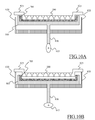
- Figure 10A is a sectional view of the bundle susceptor-tank-moving device when the mobile gathering tank 705 is in the first configuration
- Figure 10B is a sectional view of the bundle susceptor-tank-moving device when the mobile gathering tank 705 is in the second configuration.
- the moving device comprises a container element (for example implemented in CalCarb® material) 805 adapted to accommodate the mobile gathering tank 705; the container element 805 is connected to a vertical support element 810 adapted to be translated (together with the container element 805 and the mobile gathering tank 705 housed therein) along a direction perpendicular to the susceptor 200 surface by means of moving means, such as a cam element 815.
- suspension elements 820 are provided for keeping the susceptor 200 in a position which is separated from the mobile gathering tank 705 when the latter is in the second configuration.
- the suspension elements 820 are vertical elements configured to mechanical engage a corresponding protruding lateral support element 825 provided on a corresponding lateral side of the susceptor 200.
- the susceptor 200 is supported by the bottom of the mobile gathering tank 705, with the protruding elements 825 which are disengaged from the suspension elements 820, since the formers are located in a position higher than the latter.
- the cam element 815 is rotated, in such a way that the vertical support element 810 and the container element 805 translate toward the bottom. By translating, the container element 805 brings therewith (toward the bottom) the mobile gathering tank 705 and the susceptor 200 as well.
- the lateral support elements 825 engage the corresponding suspension elements 820. Consequently, while the mobile tank 705 proceeds in the descent together with the container element 805, the susceptor 200 separates therefrom, remaining bound to the suspension elements 820 in a suspended position.
- the concepts of the present invention may be applied to all those heteroepitaxiable semiconductor materials having a melting temperature higher than that of the material forming the substrate (for example, different from Si).
Landscapes
- Chemical & Material Sciences (AREA)
- Metallurgy (AREA)
- Engineering & Computer Science (AREA)
- Materials Engineering (AREA)
- Organic Chemistry (AREA)
- Crystallography & Structural Chemistry (AREA)
- Chemical Kinetics & Catalysis (AREA)
- Mechanical Engineering (AREA)
- General Chemical & Material Sciences (AREA)
- Inorganic Chemistry (AREA)
- Crystals, And After-Treatments Of Crystals (AREA)
- Liquid Deposition Of Substances Of Which Semiconductor Devices Are Composed (AREA)
- Recrystallisation Techniques (AREA)
Abstract
Description
- The present invention relates to the electronics sector. More in detail, the present invention relates to a method for manufacturing a semiconductor material wafer.
- A semiconductor electronic device, either an Integrated Circuit (IC) or a power device, is a circuit whose components are directly fabricated in a semiconductor material substrate. The substrates of the great majority of the ICs presently available on the market are obtained from silicon (Si) wafers.
- Recently, silicon carbide (SiC) wafers have been developed. Compared to silicon, silicon carbide has different chemical-physical properties, at least in part due to the different band gap value (indeed, silicon carbide has a band gap higher than that of silicon). For example, silicon carbide is characterized by a breaking voltage higher than that of the silicon, and it is thus an optimal material for manufacturing electronic devices for power applications, since a wafer (and, thus, a substrate for an IC) formed in silicon carbide is capable of managing voltages of relatively high values even with a relatively thin thickness. Moreover, using a silicon carbide wafer is particularly advantageous in all the electronic fields requiring the managing of high frequency signals.
- Silicon wafers are typically formed in pure monocrystalline silicon. A known manufacturing process for generating wafers of this type is the so-called "Czochralski growth process", which provides for introducing a monocrystalline silicon seed within a mass of melted silicon, and the gradual extraction of the seed from the melted silicon together with a slow rotation of the seed itself.
- The presently employed techniques for growing a silicon carbide crystal are very complex and expensive. Because of its peculiar physical features, a silicon carbide wafer cannot be manufactured with the methods used for manufacturing silicon wafers. Since silicon carbide is a material which directly passes (sublimates) from the solid phase to the vapour phase, without passing from any liquid phase, the Czochralski growth process cannot be used, since this latter process just requires that the seed is inserted in a melting of the desired material.
- Silicon carbide may occurs in a number of different chrystallographic structures (polytypes). Among the number of polytypes, the most common are the cubic polytype (3C polytype), the hexagonal polytype (4H and 6H polytypes), and the rhombohedric polytype (15R polytype). Presently, by means of complex and expensive processes it is possible to manufacture silicon carbide wafers of the 4H and 6H polytypes having diameters not higher than four inches starting from the corresponding crystal obtained by means of sublimation process. Such processes provides for cutting the ingot in slices, lapping, polishing of one of the two faces and then epitaxial growth.
- Being not possible to use the Czochralski growth process for manufacturing silicon carbide wafer, a possible solution for the 3C polytype (briefly, 3C SiC), may provide for using epitaxial growth techniques. As it is known to the skilled technicians, with epitaxial growth it is intended a method which provides for the deposition of thin layers of material on a crystalline substrate, which addresses its growing and determinates its structural properties. However, with the presently available technologies is very difficult obtaining a 3C SiC crystal to be used as a crystalline substrate for a subsequent epitaxial growth. In order to solve this problem, some known solutions provides for the growing of a 3C SiC layer by means of a heteroepitaxial process starting from a silicon substrate. However, such known solutions only allow the growing of layers having very thin thickness (lower than a micron) or scarce quality (high defectiveness).
- This above mentioned drawbacks do not affect the 3C SiC case only, but also other materials for which it is difficult to grow a crystal to be used as substrate for a subsequent epitaxial growth, such as for example the Gallium Nitride (GaN).
- Today, the presently available solutions do not allow to produce wafers of 3C polytype silicon carbide (and of equivalent materials) having a sufficiently high quality for the implementation of devices.
- According to an embodiment of the present invention, a possible solution of the drawbacks which affects the presently used growing processes, provides for the deposition of a first layer of the desired material on a crystalline substrate having a lower melting temperature, the subsequent elimination of the substrate by means of the melting, and the deposition of a second layer of the desired material on the first layer.
- A first aspect according to an embodiment of the present invention relates to a method for producing a wafer of a first semiconductor material. Said first semiconductor material has a first melting temperature. The method comprises providing a crystalline substrate of a second semiconductor material having a second melting temperature lower than the first melting temperature, and exposing the crystalline substrate to a flow of first material precursors for forming a first layer of the first material on the substrate. The method further comprising bringing the crystalline substrate to a first process temperature higher than the second melting temperature, and at the same time lower than the first melting temperature, in such a way the second material melts, separating the second melted material from the first layer, and exposing the first layer to the flow of the first material precursor for forming a second layer of the first material on the first layer.
- In this way it is possible to obtain material wafers with a single process, eliminating some of the process phases of the known solutions presently in use (among which cutting of the crystal in slices, lapping and polishing).
- Another aspect according to an embodiment of the present invention relates to a reaction chamber for producing a semiconductor material wafer. Such reaction chamber comprises a susceptor, heating means for heating the susceptor, and conduction means for providing a precursors flow. Said susceptor comprises a plurality of draining openings adapted to make melted material generated during the manufacturing of the semiconductor material wafer flowing out from the susceptor.
- A further aspect of the present invention relates to a semiconductor material wafer.
-
-
Figure 1 schematically illustrates, by means of a sectional view, a horizontal reaction chamber according to a known solution; -
Figure 2 schematically illustrates, by means of a sectional view, a vertical reaction chamber according to a known solution; -
Figure 3A is a view from the above of a susceptor adapted to be employed in the reaction chamber ofFigure 1 according to an embodiment of the present invention; -
Figure 3B is a sectional view of the susceptor ofFigure 3A taken along a sectional plan perpendicular to the surface of the susceptor; -
Figure 4A is a view from the above of a susceptor adapted to be employed in the reaction chamber ofFigure 1 according to a further embodiment of the present invention; -
Figure 4B is a sectional view of the susceptor of claim 4A taken along a sectional plan perpendicular to the surface of the susceptor; -
Figure 5 is a sectional view of a reaction chamber according to an embodiment of the present invention; -
Figure 6 illustrates a possible thermal profile of the reaction chamber ofFigure 5 during phases of a method for producing a semiconductor material wafer according to an embodiment of the present invention; -
Figures 7A-7D are sectional view of a semiconductor material wafer during some steps of the realization method according to an embodiment of the present invention; -
Figure 8A and Figure 8B are sectional view of a mobile gathering tank according to an embodiment of the present invention; -
Figure 9A and Figure 9B are sectional view of a mobile gathering tank according to a further embodiment of the present invention, and -
Figure 10A and Figure 10B are sectional view of a moving device of the gathering tank ofFigures 9A and 9B according to an embodiment of the present invention. - The present detailed description refers to a method for manufacturing a 3C SiC wafer by means of a Chemical Vapor Deposition (CVD) hetero-homo epitaxial growing process starting from a silicon substrate, and to a corresponding reaction chamber wherein carrying out such method.
-
Figure 1 schematically illustrates by means of a sectional view areaction chamber 100 wherein the concepts of the present invention may be applied. - Without descending into specific details which are outside the purpose of the present document, the
reaction chamber 100 comprises ahollow body 103 formed in an insulating material, adapted to thermally insulating the inner cavity from the external environment. Thereaction chamber 100 comprises a support 105 (in jargon, "susceptor") adapted to sustain the crystalline substrate (identified in figure with the reference 102) on which a 3C SiC layer is epitaxially grown, as will be described in detail in the following of the present description. Thesusceptor 105 is a substantially flat element, for example having a circular shape, implemented in a material having a high melting temperature, such as for example naked graphite having a high degree of pureness and a high dilatation coefficient. The reaction chamber comprises heating means 110 configured to heat thesusceptor 105. For example, the heating means 110 may be of the inductive type, comprising coils, or of the resistive type, comprising carbide covered resistors. - As it is known to those skilled in the art, the deposition process provides that the
substrate 102, supported and heated by thesusceptor 105, is invested by a gas flow that carries - in gaseous form - the particles of the material to be deposited on thesubstrate 102 itself; in jargon, the gas flow comprising particles of a material to be deposed is identified as "precursor" of the material itself. Aninput duct 115 is provided for inputting the precursors within thereaction chamber 100, and anoutput duct 120 is provided for discharging the reaction gases outside thereaction chamber 100. - In the
reaction chamber 100 illustrated inFigure 1 , theinput duct 115 and theoutput duct 120 are arranged in such a way that the precursor flow hits thesubstrate 102 longitudinally to the main surface of thesubstrate 102 itself. A reaction chamber of this type is in jargon referred to as horizontal flux reaction chamber. - The concepts of the present invention may be however applied to vertical flux reaction chambers, wherein the input duct and the output duct are arranged in such a way that the precursor flow hits the substrate transversally to the main surface of the substrate itself, and wherein the heating element is of the induction type. A possible example of a reaction chamber of this type is illustrated in
Figure 2 . - As will be described in detail in the following of the present invention, the method according to an embodiment of the present invention provides that from the wafer in process melted material is generated, which melted material requires to be drained and collected, for being removed in a second time. For this reason, according to an embodiment of the present invention, the susceptor is provided with draining openings for the flowing out of the melted material.
-
Figure 3A is a view from the above of asusceptor 200 according to an embodiment of the present invention;Figure 3B is a sectional view of thesusceptor 200 offigure 3A taken along a sectional plane perpendicular to the surface of thesusceptor 200 and passing from the line II-II. According to such embodiment, thesusceptor 200 comprises a plurality of circular draining openings, identified in figure with thereference 205, uniformly arranged along thesusceptor surface 205. As visible inFigure 3B , in the considered embodiment the draining openings are shaped according to a "funnel" shape, with a beginning cone-shaped portion and a terminating cylindrical portion. -
Figure 4A is a view from the above of a susceptor 200' according to a further embodiment of the present invention;Figure 4B is a sectional view of the susceptor 200' ofFigure 4A taken along a sectional plane perpendicular to the surface of the susceptor 200' and passing from the line III-III. According to such embodiment, the susceptor 200' comprises a plurality of draining openings substantially having a slit shape, identified in figure with thereference 305, in such a way to define a substantially grid structure on the surface of the susceptor. - Naturally, the
susceptors 200, 200' illustrated inFigures 3A, 3B ,4A and 4B are to be considered only for exemplificative and non limitative purposes, since the concepts of the present invention may be applied to susceptors having draining openings having different shapes and arrangements (e.g., having a polygonal shape). - Making reference to
Figure 5 , a susceptor according to the present invention - i.e., provided with draining openings - is located within thereaction chamber 100 on a support comprising a gathering tank 125 (for example, in graphite). In the illustrated example, the employed susceptor is thesusceptor 200 ofFigures 3A and 3B , provided with circular openings. However, it is underlined that same considerations apply to susceptors provided with draining openings having a different shape, such as the slit draining openings of the susceptor 200' ofFigures 4A and 4B . - A method for manufacturing a 3C SiC wafer which exploits the reaction chamber 100 (indifferently, at horizontal or vertical flow) equipped with the
susceptor 200 provided with draining openings according to an embodiment of the present invention. - It is underlined that, during the manufacturing of the 3C SiC wafer, the temperature of the reaction chamber 100 - and in particular of the susceptor 200 - is varied by properly driving the heating means 110; to this end,
Figure 6 illustrates a possiblethermal profile 400 of thereaction chamber 100 during the various phases of the method according to an embodiment of the present invention. - PHASE 1: The
reaction chamber 100 is at the room temperature. Asilicon crystalline substrate 102, for example of the (100) type, is positioned on thesusceptor 200, A situation of this type is shown inFigure 7A . - PHASE 2: The heating means 110 are activated for rising the temperature of the
reaction chamber 100 until reaching a temperature equal to about 1000-1100°C. Theducts substrate 102 in a hydrogen flow. - PHASE 3: The temperature is kept at the same value reached in the previous phase. The surface of the
substrate 102 is subjected to activation operations, for example by means H2, HCl and deposition of silicon buffer. - PHASE 4: The temperature of the
reaction chamber 100 is risen until about 1330-1380°C. A carbon precursor is added to the hydrogen flow, in order to carbonise the superficial silicon atoms of thesubstrate 102, and obtaining a thin layer, of the order of few nanometers, of SiC (in jargon, "ramp carbonisation"). Such thin layer of silicon carbide has the purpose of acting as a seed for the SiC growth which will be carried out in the following phase. - PHASE 5: Keeping the temperature of the
reaction chamber 100 at about 1330-1380°C, a silicon precursor is added to the carbon precursor. In this way, a 3C SiC layer is caused to grow from the thin layer previously generated (epitaxial grow). Since the silicon of the substrate ha a reticule that is different than the silicon carbide of the growing layer (5,43 angstrom for the silicon and 4,36 angstrom for the silicon carbide), the more the 3C Sic layer grows, the more the semiconductor wafer tends to warp. Although a semiconductor material wafer having an excessive warping cannot be used for integrating electronic devices, since the integration operations request the use of sufficiently planar wafers, this phase is however made to last a time sufficient to grow a 3C SiC layer having a thickness of some tents of microns (for example, 30-40 microns), causing a non negligible warping. A situation of this type is illustrated inFigure 7B , wherein the 3C SiC layer is identified with thereference 510. It is however underlined that the drawback of the excessive wafer warping is resolved according to the present invention in the following phases of the method which will be now described. - PHASE 6: According to an embodiment of the present invention, the temperature of the
reaction chamber 100 is risen until reaching a temperature higher than the melting temperature of the silicon, and at the same time lower than the melting temperature of the 3C SiC. For example, thereaction chamber 100 is brought to a temperature of about 1450-1460°C. - PHASE 7: The
reaction chamber 100 is kept at the temperature just reached, while the precursor flow (silicon and carbon) is kept constant with respect to the preceding phases. In this way, while the3C SiC layer 510 continues to grow in thickness, since supplied by the precursors of the silicon and of the carbon, theunderneath silicon substrate 102 starts to melt, and in the melted state passes through the draining openings of thesusceptor 200, for being collected in theunderneath gathering tank 125. With the melting, and the passage in theunderneath gathering tank 125, of an ever increasing portion of thesubstrate 102, the warping affecting the wafer tends to diminish, being the wafer made up more and more by silicon carbide and less and less by silicon. The duration of this phase is set in such a way to allow the melting and the separation of (substantially) all the silicon of thesubstrate 102. In this situation, illustrated inFigure 7C , the resulting semiconductor material wafer located on the susceptor 200 - globally identified in figure with the reference 515 - results to be solely formed by the3C SiC layer 510; the silicon collected by thegathering tank 125 after the melting of thesubstrate 102 is identified in figure with thereference 520. Being the reticular discontinuity at the interface Si-SiC no more present, theSiC layer 515 results to be planar, It is underlined that growing a3C SiC layer 510 of sufficiently high thickness (30-40 microns, see PHASE 5) before rising the temperature above the melting point of the silicon results to be very advantageous, since said SiC layer should be capable of remaining integral even without theunderneath silicon substrate 102. With a3C SiC 510 layer too much thin, thewafer 515 would risk to break further to the silicon melting. - PHASE 8: Continuing to supply the reaction chamber with the precursor flow, the thickness of the 3C SiC layer 510 (and, thus, of the SiC layer 515) continues to grow. When the thickness has reached a sufficiently high level (for example about 100 microns), the temperature of the
reaction chamber 100 is brought again to a value lower than the melting temperature of the silicon, for example at about 1370°C. In this way, the meltedsilicon 520 collected in thegathering tank 125 firms up. - PHASE 9: Keeping the
reaction chamber 100 at the temperature reached inPHASE 8, and continuing to constantly provide the flow of silicon and carbon precursors, a further layer of 3C SiC, identified inFigure 7D with thereference 530, is grown on thelayer 510 of SiC, having desired thickness and resistivity. Unlike the preceding phases, wherein the growing was of the heteroepitaxial type - indeed, other than theSiC layer 510 it was present also the silicon substrate 102 -, the growing of thelayer 530 results to be of the homoepitaxial type, since thewafer 515 results to be exclusively formed by SiC. During this phase, it is further possible to input in the chamber - together with the silicon and carbon precursors - doping elements for varying the resistivity of thelayer 530. The portion of thewafer 515 corresponding to thelayer 530 may be thus used as an active zone wherein forming the electronic devices. For example, for dopings of the N type it is possible to add nitrogen, while for dopings of the P type it is possible to add aluminium, for example in form of an organometallic compounds (trimethylaluminium). - PHASE 10: Having reached the desired thickness of the SiC layer, the temperature of the
reaction chamber 100 is taken back to the room temperature, and the precursors flow is interrupted. - At the end of the last phase of the method according to the invention, a
wafer 515 of 3C SiC is obtained as final product, having the desired thickness and resistivity and a good planarity degree, and a mass of polycrystalline silicon as waste product. - According to another embodiment of the present invention, the 3C SiC wafer fabrication method above described may be optimised using a reaction chamber with a mobile gathering tank, adapted to pass in a particular phases of the growing process from a first configuration, wherein the tank is in contact with the susceptor and forms therewith a single body, to a second configuration, wherein the tank and the susceptor are separated, and viceversa.
-
Figure 8A is a sectional view of a mobile gathering tank according to an embodiment of the present invention, identified with thereference 605, in the first configuration, whileFigure 8B is a sectional view of the samemobile gathering tank 605 in the second configuration. According to an embodiment of the present invention, themobile gathering tank 605 comprises a plurality of protrudingelements 610 that protrude from the bottom of the tank itself; each protrudingelement 610 is adapted to engage a respective draining opening of thesusceptor 200 when themobile gathering tank 605 is in the first configuration. As visible inFigure 8A , when themobile gathering tank 605 is in the first configuration, the draining openings of thesusceptor 200 are closed; in this configuration, the gathering of melted material in the tank is prevented, allowing, in some phases of the wafer manufacturing method, the coexistence of the 3C SiC solid mass in contact with the liquid mass of the melted Si. Themobile gathering tank 605 is configured to be moved perpendicularly to thesusceptor surface 200 in such a way to disengage theprotruding elements 610 from the respective draining openings of thesusceptor 200. In this configuration, visible inFigure 8B , the draining openings of the susceptor are open, allowing thus the gathering of melted material in the tank. - As already mentioned, the
mobile gathering tank 605 may be advantageously employed for optimising the method previously described. Such optimisation provides for performing the previously described method until the phase wherein the temperature is risen above the silicon melting temperature (PHASE 6) with themobile gathering tank 605 kept in the first configuration (draining openings closed). Since the draining openings of thesusceptors 200 are closed, the melted Si which is produced because of the high temperature cannot flow out. Themobile gathering tank 605 is kept in the first configuration during all the SiC deposition phase; in this way, a more uniform heat distribution occurs between the wafer and the susceptor, and the solid mass of SiC is in contact with the melted mass of Si during the whole SiC deposition phase. Once the desired SiC thickness is reached, always keeping the temperature of the reaction chamber at the temperature reached in the previous phase, themobile gathering tank 605 is lowered and brought in the second configuration, in such a way to free the draining openings of thesusceptor 200; at the same time, the reaction chamber is brought back to the room temperature. In this way, the melted silicon flows in themobile gathering tank 605 passing through the draining openings. Unlike the preceding case (fixed gathering tank), wherein the separation between Si and SiC was only caused by the rising of the chamber temperature above the melting temperature, in this case the separation is further favoured by the dragging mechanical action of the melted silicon toward the bottom caused by the lowering of themobile gathering tank 605. -
Figure 9A and Figure 9B show amobile gathering tank 705 according to a further embodiment of the present invention, wherein themobile gathering tank 705 has the bottom voids of protruding elements.Figure 9A is a sectional view of themobile gathering tank 705 in the first configuration, whileFigure 9B is a sectional view of themobile gathering tank 705 in the second configuration. Even according to such embodiment, in the first configuration the draining openings of thesusceptors 200 results to be closed, preventing the gathering of melted material in the tank, while in the second configuration the draining openings of the susceptors results to be open, allowing the gathering of melted material in the tank. Themobile gathering tank 705 may be employed in the same way as themobile gathering tank 605. - A possible implementation of a moving device adapted to vertically move a mobile gathering tank according to the present invention (for example, the
mobile gathering tank 705 voids of protruding elements) is illustrated inFigures 10A and 10B. Figure 10A is a sectional view of the bundle susceptor-tank-moving device when themobile gathering tank 705 is in the first configuration, whileFigure 10B is a sectional view of the bundle susceptor-tank-moving device when themobile gathering tank 705 is in the second configuration. According to an embodiment of the present invention, the moving device comprises a container element (for example implemented in CalCarb® material) 805 adapted to accommodate themobile gathering tank 705; thecontainer element 805 is connected to avertical support element 810 adapted to be translated (together with thecontainer element 805 and themobile gathering tank 705 housed therein) along a direction perpendicular to thesusceptor 200 surface by means of moving means, such as acam element 815. According to an embodiment of the present invention,suspension elements 820 are provided for keeping thesusceptor 200 in a position which is separated from themobile gathering tank 705 when the latter is in the second configuration. According to an embodiment of the present invention, thesuspension elements 820 are vertical elements configured to mechanical engage a corresponding protrudinglateral support element 825 provided on a corresponding lateral side of thesusceptor 200. When themobile gathering tank 705 is in the first configuration, thesusceptor 200 is supported by the bottom of themobile gathering tank 705, with the protrudingelements 825 which are disengaged from thesuspension elements 820, since the formers are located in a position higher than the latter. In order to pass to the second configuration, thecam element 815 is rotated, in such a way that thevertical support element 810 and thecontainer element 805 translate toward the bottom. By translating, thecontainer element 805 brings therewith (toward the bottom) themobile gathering tank 705 and thesusceptor 200 as well. During the translation toward the bottom of thecontainer element 805, at a certain point thelateral support elements 825 engage thecorresponding suspension elements 820. Consequently, while themobile tank 705 proceeds in the descent together with thecontainer element 805, thesusceptor 200 separates therefrom, remaining bound to thesuspension elements 820 in a suspended position. - Although in the present description it has been largely discussed a method for producing 3C SiC wafers starting from a Si substrate, the concepts of the present invention (included the use of susceptors provided with draining openings and/or the use of mobile gathering tanks) may be applied to all those heteroepitaxiable semiconductor materials having a melting temperature higher than that of the material forming the substrate (for example, different from Si).
Claims (14)
- Method for manufacturing a wafer of a first semiconductor material (515) having a first melting temperature, comprising:- providing a crystalline substrate (102) of a second semiconductor material having a second melting temperature lower than the first melting temperature;- exposing the crystalline substrate to a flow of first material precursors for forming a first layer (510) of the first material on the substrate;- bringing the crystalline substrate to a first process temperature higher than the second melting temperature, and at the same time lower than the first melting temperature, in such a way that the second material melts;- separating the second melted material from the first layer, and- exposing the first layer to the flow of first material precursors for forming a second layer (530) of the first material on the first layer.
- The method according to claim 1, wherein:- said exposing the crystalline substrate to a flow of the first material precursors for forming said first layer (510) and- said exposing the first layer to a flow of first material precursors for forming said second layer (530)
are carried out at a second process temperature lower than the second melting temperature. - The method according to claim 1 or claim 2, wherein said first material is silicon carbide of the 3C polytype and said second material is crystalline silicon.
- The method according to any one among the preceding claims when depending on claim 2, further comprising activating a surface of the crystalline substrate before exposing said crystalline substrate to the flow of first material precursors for forming the first layer, said activating being carried out at a third process temperature lower than the second process temperature.
- The method according to any one among the preceding claims, wherein:- said forming the first layer comprises heteroepitaxially growing said first layer on the substrate, and- said forming the second substrate comprises homoepitaxially growing said second layer on said first layer.
- The method according to any one among the preceding claims, further comprising:maintaining the first layer in contact with the second melted material at least when the crystalline substrate is brought to the first process temperature.
- Reaction chamber (100) for manufacturing a semiconductor material wafer, said reaction chamber comprising:- a susceptor (200);- heating means (110) for heating the susceptor;- conduction means (115, 120) for providing a precursors flow,
characterized in that- said susceptor comprises a plurality of draining openings (205; 305) adapted to make melted material generated during the manufacturing of the semiconductor material wafer flowing out from the susceptor. - Reaction chamber according to claim 7, further comprising a gathering tank (125; 605; 705) for gathering the melted material flowed out from the draining openings.
- Reaction chamber according to claim 8, wherein said susceptor and said gathering tank are formed in graphite.
- Reaction chamber according to claim 8 or claim 9, wherein said gathering tank (605; 705) is configured to pass
from- a first configuration, wherein the tank is in contact with the susceptor and forms therewith a single body,to- a second configuration, wherein the tank and the susceptor are detached,and viceversa. - Reaction chamber according to claim 10, wherein:- when the gathering tank is in the first configuration, said draining openings are closed by the gathering tank, in such a way to impede the flowing out of the melted material and allow the coexistence of the melted material in contact with the semiconductor material wafer.
- Reaction chamber according to claim 11, wherein the gathering tank (605) comprises a plurality of protruding elements (610) configured to engage the draining openings of the susceptor when the gathering tank is in the first configuration.
- Use of the reaction chamber according to any one among claims 7 to 12 for producing a semiconductor material wafer according to the method according to any one among claims 1 to 5.
- Semiconductor material wafer manufactured according to any one among the preceding claims.
Applications Claiming Priority (1)
| Application Number | Priority Date | Filing Date | Title |
|---|---|---|---|
| IT002273A ITMI20112273A1 (en) | 2011-12-15 | 2011-12-15 | METHOD FOR THE PRODUCTION OF A SLICE OF SILICON CARBIDE AND ITS EQUIPMENT |
Publications (1)
| Publication Number | Publication Date |
|---|---|
| EP2604729A1 true EP2604729A1 (en) | 2013-06-19 |
Family
ID=45571667
Family Applications (1)
| Application Number | Title | Priority Date | Filing Date |
|---|---|---|---|
| EP12195884.7A Withdrawn EP2604729A1 (en) | 2011-12-15 | 2012-12-06 | Method for manufacturing a silicon carbide wafer and respective equipment |
Country Status (3)
| Country | Link |
|---|---|
| US (2) | US9406504B2 (en) |
| EP (1) | EP2604729A1 (en) |
| IT (1) | ITMI20112273A1 (en) |
Cited By (1)
| Publication number | Priority date | Publication date | Assignee | Title |
|---|---|---|---|---|
| EP4006954A1 (en) * | 2020-11-27 | 2022-06-01 | STMicroelectronics S.r.l. | Manufacturing method of a sic wafer with residual stress control |
Families Citing this family (10)
| Publication number | Priority date | Publication date | Assignee | Title |
|---|---|---|---|---|
| JP6643029B2 (en) * | 2015-10-06 | 2020-02-12 | 東洋炭素株式会社 | Heat treatment container and etching method for single crystal silicon carbide substrate |
| ITUA20162943A1 (en) * | 2016-04-27 | 2017-10-27 | Pilegrowth Tech S R L | Method for the industrial manufacture of a semiconductor structure with reduced bowing. |
| US10475673B2 (en) * | 2016-09-28 | 2019-11-12 | Stmicroelectronics S.R.L. | Apparatus for manufacturing a silicon carbide wafer |
| US11309177B2 (en) | 2018-11-06 | 2022-04-19 | Stmicroelectronics S.R.L. | Apparatus and method for manufacturing a wafer |
| IT201900015416A1 (en) | 2019-09-03 | 2021-03-03 | St Microelectronics Srl | APPARATUS FOR GROWING A SLICE OF SEMICONDUCTOR MATERIAL, IN PARTICULAR SILICON CARBIDE, AND ASSOCIATED MANUFACTURING PROCESS |
| JP7363591B2 (en) * | 2020-03-05 | 2023-10-18 | 東京エレクトロン株式会社 | Substrate processing equipment and substrate processing method |
| IT202000026356A1 (en) | 2020-11-05 | 2022-05-05 | Pilegrowth Tech S R L | METHOD FOR PRODUCING A SELF-SUPPORTING AND STRESS-FREE EPITAXY LAYER FROM A DISPOSABLE SUBSTRATE MOLDED IN THE FORM OF AN EXCAVATED PILLARS MATRIX |
| CN114561705B (en) * | 2020-11-27 | 2024-11-29 | 意法半导体股份有限公司 | Method for manufacturing SiC wafer with residual stress control |
| JP2024102694A (en) | 2023-01-19 | 2024-07-31 | 信越半導体株式会社 | Manufacturing method of 3C-SiC single crystal epitaxial substrate, manufacturing method of 3C-SiC free-standing substrate, and 3C-SiC single crystal epitaxial substrate |
| CN116230597B (en) * | 2023-05-09 | 2023-09-08 | 内蒙古晶环电子材料有限公司 | Hydrogen etching tool and method for silicon carbide wafer |
Citations (4)
| Publication number | Priority date | Publication date | Assignee | Title |
|---|---|---|---|---|
| US4537651A (en) * | 1981-05-22 | 1985-08-27 | United Technologies Corporation | Method for removing semiconductor layers from salt substrates |
| US4574730A (en) * | 1984-02-27 | 1986-03-11 | Northern Telecom Limited | Melt dispensing liquid phase epitaxy boat |
| US4582561A (en) * | 1979-01-25 | 1986-04-15 | Sharp Kabushiki Kaisha | Method for making a silicon carbide substrate |
| US5183529A (en) * | 1990-10-29 | 1993-02-02 | Ford Motor Company | Fabrication of polycrystalline free-standing diamond films |
Family Cites Families (7)
| Publication number | Priority date | Publication date | Assignee | Title |
|---|---|---|---|---|
| US3777009A (en) * | 1971-08-05 | 1973-12-04 | Little Inc A | Method for direct melt synthesis of intermetallic compounds |
| IL98530A (en) | 1990-06-25 | 1996-06-18 | Lanxide Technology Co Ltd | Methods for making selfsupporting composite bodies and articles produced thereby using vapor-phase parent metals and solid oxidants |
| JP3707726B2 (en) * | 2000-05-31 | 2005-10-19 | Hoya株式会社 | Silicon carbide manufacturing method, composite material manufacturing method |
| CN1243855C (en) * | 2000-06-15 | 2006-03-01 | 六号元素(控股)公司 | Single Crystal Diamond Prepared by CVD |
| US8277760B2 (en) | 2003-09-19 | 2012-10-02 | Applied Biosystems, Llc | High density plate filler |
| DE102006017621B4 (en) * | 2006-04-12 | 2008-12-24 | Schott Ag | Apparatus and method for producing multicrystalline silicon |
| PL3099440T3 (en) | 2014-01-27 | 2025-12-22 | Rovalma, S.A. | Centrifugal atomization of iron-based alloys |
-
2011
- 2011-12-15 IT IT002273A patent/ITMI20112273A1/en unknown
-
2012
- 2012-12-06 EP EP12195884.7A patent/EP2604729A1/en not_active Withdrawn
- 2012-12-13 US US13/714,277 patent/US9406504B2/en active Active
-
2016
- 2016-06-27 US US15/194,309 patent/US10153207B2/en active Active
Patent Citations (4)
| Publication number | Priority date | Publication date | Assignee | Title |
|---|---|---|---|---|
| US4582561A (en) * | 1979-01-25 | 1986-04-15 | Sharp Kabushiki Kaisha | Method for making a silicon carbide substrate |
| US4537651A (en) * | 1981-05-22 | 1985-08-27 | United Technologies Corporation | Method for removing semiconductor layers from salt substrates |
| US4574730A (en) * | 1984-02-27 | 1986-03-11 | Northern Telecom Limited | Melt dispensing liquid phase epitaxy boat |
| US5183529A (en) * | 1990-10-29 | 1993-02-02 | Ford Motor Company | Fabrication of polycrystalline free-standing diamond films |
Cited By (1)
| Publication number | Priority date | Publication date | Assignee | Title |
|---|---|---|---|---|
| EP4006954A1 (en) * | 2020-11-27 | 2022-06-01 | STMicroelectronics S.r.l. | Manufacturing method of a sic wafer with residual stress control |
Also Published As
| Publication number | Publication date |
|---|---|
| US20130157448A1 (en) | 2013-06-20 |
| US9406504B2 (en) | 2016-08-02 |
| US20160307800A1 (en) | 2016-10-20 |
| US10153207B2 (en) | 2018-12-11 |
| ITMI20112273A1 (en) | 2013-06-16 |
Similar Documents
| Publication | Publication Date | Title |
|---|---|---|
| US10153207B2 (en) | Method for manufacturing a silicon carbide wafer using a susceptor having draining openings | |
| US8313720B2 (en) | Guided diameter SiC sublimation growth with multi-layer growth guide | |
| CN101553604B (en) | Process for producing single crystal of silicon carbide | |
| US7300519B2 (en) | Reduction of subsurface damage in the production of bulk SiC crystals | |
| JP5526866B2 (en) | Silicon carbide crystal manufacturing method and silicon carbide crystal manufacturing apparatus | |
| KR100773624B1 (en) | Seed crystal consisting of silicon carbide single crystal and method for producing ingot using same | |
| JP2010095397A (en) | Silicon carbide single crystal and silicon carbide single crystal wafer | |
| JP2021050112A (en) | Manufacturing method of silicon carbide single crystal wafer and silicon carbide single crystal ingot | |
| EP1797225A2 (en) | Low 1c screw dislocation density 3 inch silicon carbide wafer | |
| CN104350187A (en) | Method for manufacturing silicon carbide substrate | |
| JP5829508B2 (en) | Crystal growth method of SiC crystal and SiC crystal substrate | |
| JP5440260B2 (en) | Method for manufacturing silicon carbide crystal and apparatus for manufacturing the same | |
| US20130068157A1 (en) | Method of manufacturing silicon carbide crystal | |
| JP4733485B2 (en) | Method for producing seed crystal for silicon carbide single crystal growth, seed crystal for silicon carbide single crystal growth, method for producing silicon carbide single crystal, and silicon carbide single crystal | |
| JP2005239496A (en) | Silicon carbide raw material for growing silicon carbide single crystal, silicon carbide single crystal and method for producing the same | |
| JP5761264B2 (en) | Method for manufacturing SiC substrate | |
| CN114351253B (en) | Method and apparatus for producing silicon carbide single crystal, and silicon carbide single crystal ingot | |
| JP5333363B2 (en) | Silicon carbide raw material for growing silicon carbide single crystal and method for producing silicon carbide single crystal using the same | |
| JP5163445B2 (en) | Crystal manufacturing method | |
| JP7476890B2 (en) | Method for manufacturing SiC single crystal ingot | |
| JP5549722B2 (en) | Crystal manufacturing method | |
| JP2000026199A (en) | Method for producing silicon carbide single crystal and silicon carbide single crystal | |
| Balakrishnan et al. | Sublimation growth of AlN bulk crystals by seeded and spontaneous nucleation methods |
Legal Events
| Date | Code | Title | Description |
|---|---|---|---|
| PUAI | Public reference made under article 153(3) epc to a published international application that has entered the european phase |
Free format text: ORIGINAL CODE: 0009012 |
|
| AK | Designated contracting states |
Kind code of ref document: A1 Designated state(s): AL AT BE BG CH CY CZ DE DK EE ES FI FR GB GR HR HU IE IS IT LI LT LU LV MC MK MT NL NO PL PT RO RS SE SI SK SM TR |
|
| AX | Request for extension of the european patent |
Extension state: BA ME |
|
| 17P | Request for examination filed |
Effective date: 20131218 |
|
| RBV | Designated contracting states (corrected) |
Designated state(s): AL AT BE BG CH CY CZ DE DK EE ES FI FR GB GR HR HU IE IS IT LI LT LU LV MC MK MT NL NO PL PT RO RS SE SI SK SM TR |
|
| 17Q | First examination report despatched |
Effective date: 20150715 |
|
| STAA | Information on the status of an ep patent application or granted ep patent |
Free format text: STATUS: THE APPLICATION IS DEEMED TO BE WITHDRAWN |
|
| 18D | Application deemed to be withdrawn |
Effective date: 20151126 |