EP2602818A1 - An interposer device - Google Patents
An interposer device Download PDFInfo
- Publication number
- EP2602818A1 EP2602818A1 EP11306634.4A EP11306634A EP2602818A1 EP 2602818 A1 EP2602818 A1 EP 2602818A1 EP 11306634 A EP11306634 A EP 11306634A EP 2602818 A1 EP2602818 A1 EP 2602818A1
- Authority
- EP
- European Patent Office
- Prior art keywords
- layer
- silicon substrate
- trench
- doped silicon
- conductive layers
- Prior art date
- Legal status (The legal status is an assumption and is not a legal conclusion. Google has not performed a legal analysis and makes no representation as to the accuracy of the status listed.)
- Withdrawn
Links
Images


Classifications
-
- H—ELECTRICITY
- H10—SEMICONDUCTOR DEVICES; ELECTRIC SOLID-STATE DEVICES NOT OTHERWISE PROVIDED FOR
- H10W—GENERIC PACKAGES, INTERCONNECTIONS, CONNECTORS OR OTHER CONSTRUCTIONAL DETAILS OF DEVICES COVERED BY CLASS H10
- H10W20/00—Interconnections in chips, wafers or substrates
- H10W20/20—Interconnections within wafers or substrates, e.g. through-silicon vias [TSV]
-
- H—ELECTRICITY
- H10—SEMICONDUCTOR DEVICES; ELECTRIC SOLID-STATE DEVICES NOT OTHERWISE PROVIDED FOR
- H10D—INORGANIC ELECTRIC SEMICONDUCTOR DEVICES
- H10D84/00—Integrated devices formed in or on semiconductor substrates that comprise only semiconducting layers, e.g. on Si wafers or on GaAs-on-Si wafers
- H10D84/201—Integrated devices formed in or on semiconductor substrates that comprise only semiconducting layers, e.g. on Si wafers or on GaAs-on-Si wafers characterised by the integration of only components covered by H10D1/00 or H10D8/00, e.g. RLC circuits
- H10D84/204—Integrated devices formed in or on semiconductor substrates that comprise only semiconducting layers, e.g. on Si wafers or on GaAs-on-Si wafers characterised by the integration of only components covered by H10D1/00 or H10D8/00, e.g. RLC circuits of combinations of diodes or capacitors or resistors
- H10D84/221—Integrated devices formed in or on semiconductor substrates that comprise only semiconducting layers, e.g. on Si wafers or on GaAs-on-Si wafers characterised by the integration of only components covered by H10D1/00 or H10D8/00, e.g. RLC circuits of combinations of diodes or capacitors or resistors of only diodes
-
- H—ELECTRICITY
- H10—SEMICONDUCTOR DEVICES; ELECTRIC SOLID-STATE DEVICES NOT OTHERWISE PROVIDED FOR
- H10W—GENERIC PACKAGES, INTERCONNECTIONS, CONNECTORS OR OTHER CONSTRUCTIONAL DETAILS OF DEVICES COVERED BY CLASS H10
- H10W20/00—Interconnections in chips, wafers or substrates
- H10W20/01—Manufacture or treatment
- H10W20/021—Manufacture or treatment of interconnections within wafers or substrates
- H10W20/023—Manufacture or treatment of interconnections within wafers or substrates the interconnections being through-semiconductor vias
-
- H—ELECTRICITY
- H10—SEMICONDUCTOR DEVICES; ELECTRIC SOLID-STATE DEVICES NOT OTHERWISE PROVIDED FOR
- H10W—GENERIC PACKAGES, INTERCONNECTIONS, CONNECTORS OR OTHER CONSTRUCTIONAL DETAILS OF DEVICES COVERED BY CLASS H10
- H10W20/00—Interconnections in chips, wafers or substrates
- H10W20/20—Interconnections within wafers or substrates, e.g. through-silicon vias [TSV]
- H10W20/211—Through-semiconductor vias, e.g. TSVs
- H10W20/217—Through-semiconductor vias, e.g. TSVs comprising ring-shaped isolation structures outside of the via holes
-
- H—ELECTRICITY
- H10—SEMICONDUCTOR DEVICES; ELECTRIC SOLID-STATE DEVICES NOT OTHERWISE PROVIDED FOR
- H10H—INORGANIC LIGHT-EMITTING SEMICONDUCTOR DEVICES HAVING POTENTIAL BARRIERS
- H10H20/00—Individual inorganic light-emitting semiconductor devices having potential barriers, e.g. light-emitting diodes [LED]
- H10H20/80—Constructional details
- H10H20/85—Packages
- H10H20/857—Interconnections, e.g. lead-frames, bond wires or solder balls
-
- H—ELECTRICITY
- H10—SEMICONDUCTOR DEVICES; ELECTRIC SOLID-STATE DEVICES NOT OTHERWISE PROVIDED FOR
- H10W—GENERIC PACKAGES, INTERCONNECTIONS, CONNECTORS OR OTHER CONSTRUCTIONAL DETAILS OF DEVICES COVERED BY CLASS H10
- H10W70/00—Package substrates; Interposers; Redistribution layers [RDL]
- H10W70/60—Insulating or insulated package substrates; Interposers; Redistribution layers
- H10W70/62—Insulating or insulated package substrates; Interposers; Redistribution layers characterised by their interconnections
- H10W70/63—Vias, e.g. via plugs
- H10W70/635—Through-vias
-
- H—ELECTRICITY
- H10—SEMICONDUCTOR DEVICES; ELECTRIC SOLID-STATE DEVICES NOT OTHERWISE PROVIDED FOR
- H10W—GENERIC PACKAGES, INTERCONNECTIONS, CONNECTORS OR OTHER CONSTRUCTIONAL DETAILS OF DEVICES COVERED BY CLASS H10
- H10W70/00—Package substrates; Interposers; Redistribution layers [RDL]
- H10W70/60—Insulating or insulated package substrates; Interposers; Redistribution layers
- H10W70/62—Insulating or insulated package substrates; Interposers; Redistribution layers characterised by their interconnections
- H10W70/65—Shapes or dispositions of interconnections
-
- H—ELECTRICITY
- H10—SEMICONDUCTOR DEVICES; ELECTRIC SOLID-STATE DEVICES NOT OTHERWISE PROVIDED FOR
- H10W—GENERIC PACKAGES, INTERCONNECTIONS, CONNECTORS OR OTHER CONSTRUCTIONAL DETAILS OF DEVICES COVERED BY CLASS H10
- H10W70/00—Package substrates; Interposers; Redistribution layers [RDL]
- H10W70/60—Insulating or insulated package substrates; Interposers; Redistribution layers
- H10W70/67—Insulating or insulated package substrates; Interposers; Redistribution layers characterised by their insulating layers or insulating parts
- H10W70/69—Insulating materials thereof
- H10W70/698—Semiconductor materials that are electrically insulating, e.g. undoped silicon
-
- H—ELECTRICITY
- H10—SEMICONDUCTOR DEVICES; ELECTRIC SOLID-STATE DEVICES NOT OTHERWISE PROVIDED FOR
- H10W—GENERIC PACKAGES, INTERCONNECTIONS, CONNECTORS OR OTHER CONSTRUCTIONAL DETAILS OF DEVICES COVERED BY CLASS H10
- H10W90/00—Package configurations
Definitions
- This invention relates generally to 3D integrated circuits or packages and, more particularly, to a silicon interposer allowing top to bottom conduction thanks to through silicon vias and to a method for manufacturing the same.
- High brightness LEDs are very sensitive to electrostatic discharge (ESD) and to the thermal coefficient of expansion (TCE) of their packages.
- ESD electrostatic discharge
- TCE thermal coefficient of expansion
- naked LED chips mounted on a silicon interposer that improves the TCE mismatch and also provides ESD protection with integrated diodes.
- Devices integration and good thermal conductivity are the key advantages of the silicon submounts.
- surface mount technology is more and more used.
- Top to bottom connexions are necessary on the submount. The top to bottom connections are provided by through vias.
- a typical manufacturing process of a through via includes forming of through via holes and deposition of a diffusion barrier layer and a conductive seed layer. A conductive material is then electroplated into the holes. Copper is typically used as the conductive material, as copper has good thermal and electrical conductivity and is available in a highly pure state. Through via may have high aspect ratios, therefore depositing copper into such structures can be challenging.
- an interposer device comprising:
- An embodiment of the invention proposes an interposer device comprising a doped silicon substrate with a concentration of dopants in a range of, for example, 10 17 to 10 20 atoms per cubic centimetres, preferably the concentration of dopants is about 10 19 atoms per cubic centimetres.
- an interposer according to the invention does not necessitate the use of a conductive material different from the material of the interposer for building the through vias. Therefore, the production costs are reduced. Indeed, no specific equipments are required, the manufacturing processes are simpler. Furthermore, the invention prevents the use of copper for filling the through vias that may causes contaminations detrimental for the LEDs implanted on the interposer.
- an interposer device comprising the steps of:
- this process is easy to implement and decreases the cost of via processing for the silicon interposer.
- a pair of Zener diodes in a back to back configuration as a bipolar transistor.
- Higher doping rates can be used in the epitaxial zone at equivalent Zener tension, allowing increased doping of the base of the parasitic bipolar transistor and consequently reducing its gain.
- the use of an isolation trench between the diodes extends the effective length of the base of the parasitic transistor, reducing its gain.
- the combination of a higher doping rate and a longer insulation trench allows to lower the gain of transistor and to make the system immune to the conduction trigger of the parasitic bipolar transistor.
- the interposer base of the present invention advantageously uses a process of planarization containing three levels of photo-etching insuring the planarization for every level of interconnection that comprises an insulation layer and a metallic level.
- FIG. 1 An embodiment of a silicon interposer according to the invention is presented in Figure 1 , in which a doped silicon substrate 1 is surmounted by an epitaxial layer 2 on its top side.
- the interposer comprises two through silicon vias 12 and 11. Said through silicon vias 12 and 11 insure electrical conduction between the top side of the epitaxial layer 2 and the bottom side of the doped silicon substrate 1.
- Silicon through vias 11 and 12 comprise a volume of the doped silicon substrate 1 and of the epitaxial layer 2 delimited by surrounding trenches 7, said trenches 7 extending from the top side of the epitaxial layer 2 to the bottom side of the doped silicon substrate 1.
- the resistivity of the through vias 11 and 12 can be adjusted depending on the dopant concentration on the doped silicon substrate 1.
- the doped silicon substrate is doped with N type dopants.
- the concentration of dopants is in a range of 10 17 to 10 20 atoms per cubic centimetres.
- the area of the through silicon vias 11 and 12 can be very large.
- a large section minimized the vias electrical resistivity.
- the ratio H/S of said through vias 11 and 12 is smaller or equal to 1, with H the average distance between the first and second side of the through vias 11 and 12 and S the average width of said through vias 11 and 12.
- the parameter p can be adapted depending on the concentration of dopants in the doped silicon substrate 1.
- the parameter H/A can be chosen by the manufacturer of an interposer according to the invention. Therefore, the electrical resistance of a through silicon via according to the invention may be easily adapted depending on the application of the through silicon via.
- the isolation between the via 11 or 12 and the external portion of silicon of the doped silicon substrate 1 is performed by surrounding trenches 7.
- Said surrounding trenches 7 are, at least, partially filled with an isolating material.
- the isolating material is a thermal silicon oxide and/or other dielectric.
- the trenches 7 are further completely filled with a dielectric.
- the trenches 7 are filled by conformal deposition of alpha silicon or polysilicon or other insulating material.
- the depth of said surrounding trenches 7 is in the range of 200 to 700 ⁇ m, for example 200 to 300 ⁇ m.
- the isolation between the two through silicon vias 12 and 11 is completed by an oxide layer 3 deposited on the top side of the epitaxial layer 2 and an oxide layer 31 deposited on the bottom side of the doped silicon substrate 1.
- Each of the said through silicon vias 11 and 12 is electrically connected to first electrodes 112 and 122 and to second electrodes 111 and 121 situated respectively on first and second side of the doped silicon substrate 1.
- the through silicon vias 11 and 12 provide top to bottom conduction through the doped silicon substrate 1.
- said through silicon vias 12 and 11 provide top to bottom conduction through the doped silicon substrate 1 and the epitaxial layer 2.
- the through silicon vias 11 and 12 are also connected to each other by two diodes 35 integrated in the epitaxial layer 2 disposed back to back and forming a back-to-back diode. Each of the said diodes 35 is connected to the adjacent top electrode 112 and 122.
- the diodes 35 comprise a portion of the epitaxial layer 25 which is doped with a different type of dopant than the doped silicon substrate 1.
- the doped silicon substrate is doped with N-type dopants and the epitaxial portions 25 are doped with P-type dopants, and the diodes 35 are PN silicon diodes.
- said diodes 35 are highly integrated in the silicon submount whatever the level of breakdown voltage of these diodes 35.
- the isolation between the two back to back diodes is performed by a diode trench 6.
- Said diode trench 6 is, at least, partially filled with an isolating material.
- the isolating material is a thermal silicon oxide and/or other dielectric.
- the trench 6 is further completely filled with a dielectric.
- the trench 6 is filled by conformal deposition of alpha silicon or polysilicon or other insulating material.
- the depth of said diode trench 6 is in the range of 1 to 20 ⁇ m. More preferably, the diode trench is of a depth at least that of the epitaxial layer thereby protecting the continuity of the electric connection between the diodes.
- the thickness of said diode trench 6 is in the range of 0.8 to 1 ⁇ m.
- the interposer also comprises a passivation layer 9 situated between the two top electrodes 112 and 122.
- said passivation layer 9 insures that the two top electrodes are connected each other only by the diodes 35.
- the portions 24, of the epitaxial layer 2, being included in the through silicon vias 11 and 12, are highly doped with dopants of the same type as the dopants of the doped silicon substrate 1.
- the doped silicon substrate 1 is doped with N-type dopant
- the epitaxial portions 24 are also doped with N-type dopants.
- the concentration of dopant in the portions 24 of the epitaxial layer is higher than the concentration if dopant in the silicon substrate 1.
- the concentration of dopant is in a range of 10 17 to 10 20 atoms per cubic centimetres.
- the doped portion 24 of a through silicon via 11 or 12 insure a deep well electrical contact with the top electrode 112 and 122 with which the vias 11 or 12 are connected.
- the peripheral insulation of the back-to-back diode facilitates the use of higher doping rates for the epitaxial layer at equivalent Zener tension allowing increased doping of the base of the parasitic bipolar transistor and consequently reducing its gain.
- the use of an isolation trench between the diodes extends the effective length of the base of the parasitic transistor, reducing its gain. For example, the combination of a higher doping rate and longer insulation trench lowers the gain of transistors to a value of less than one, making the system immune to the conduction trigger of the parasitic bipolar transistor.
- the top electrodes 112 and 122 comprise at least one metallic layer. Said metallic layer is deposited on the portion of the doped silicon substrate 1 that constitute a through silicon via 11 or 12 and on the adjacent doped portion 25 of the epitaxial layer 2.
- the top electrodes are made of aluminium or copper.
- the first metallic layer is plated with gold alloy, for example TiNiAu or TiPtAu.
- the bottom electrodes 111 and 121 comprise at least one metallic layer deposited on the side of the through silicon via opposing to the top electrode 112 and 122 respectively.
- said electrodes 111 and 121 are made of aluminium, copper, or gold alloy, for example TiNiAu or TiPtAu.
- the interposer also comprises a passivation layer 9 situated between the two top electrodes 112 and 122.
- said passivation layer 9 insures that the two top electrodes 102 are connected each other only by the diodes 35.
- FIG. 2 an exemplary embodiment of a manufacturing method according to the invention for an interposer as shown in figure 1 is described in detail.
- N type dopant for example Arsenic or Antimony or Phosphorus
- concentration of dopants is in a range of 10 17 to 10 20 atoms per cubic centimetres.
- the resistivity of the silicon substrate 1 can be adjusted, depending on the dopant concentration.
- an epitaxial layer 2 is deposited on top of the silicon substrate 1.
- the thickness and the resistivity of said epitaxial layer 2 may be chosen according to the desired electrical characteristics of the diodes 35.
- the first step further comprises the growth of a silicon oxide layer 3 above the epitaxial layer 2.
- a P or N doped layer 5 is needed.
- the silicon substrate 1 is doped with N dopants, it is necessary to deposit a P doped layer 5.
- N doped layers 4 are deposited on the epitaxial layer 2. If the silicon substrate 1 is doped with N dopants, it is necessary to deposit a N doped layer 4.
- the deposition of said doped layers 4 and 5 is performed by implant or by vapour deposition.
- deep surrounding trenches 7 are etched. These surrounding trenches 7 are situated between said layers 4 and 5.
- the depth of the surrounding trenches 7 is lower than the thickness of the silicon substrate 1, but is greater or equal than the final thickness of the interposer.
- the surrounding trenches 7 may be etched all the way through the doped silicon substrate 1.
- the surrounding trenches 7 define the volume of the doped silicon substrate 1 that will constitute the through silicon vias 11 and 12 between the top electrodes 112 and 122 and the bottom electrodes 111 and 121.
- the through silicon vias are connected by a diode.
- a non-through trench 6 is etched.
- said trench 6 separates the doped layer 5 in two subparts 51.
- these subparts 51 will provides the diodes 35 in a further step of the manufacturing process.
- the diode trench 6 will provide the isolation between the two diodes 35 disposed back to back.
- the diode trench 6 is smaller than the surrounding trenches 7. For example, the diode trench 6 is less deep than the surrounding trenches 7.
- the depth of the trench 6 is in the range of 1 to 20 ⁇ m
- the depth of the surrounding trenches 7 is in the range of 200 to 700 ⁇ m, for example 200 to 300 ⁇ m.
- the depth and the width of both types of trenches are substantially proportional.
- the width of the trenches 6 and 7 has to be quite narrow in order to facilitate the filling of said trenches in a further step of the manufacturing process.
- step D the interposer is treated in order to make diffuse the N dopants of the doped layers 4 and the P dopants of the doped layer 5 deposited in step B.
- the diodes 35 are constituted by the PN junction between the doped silicon substrate 1 and the said volume of epitaxial layer 2 wherein the dopants of the doped layer 5 have diffused.
- the dopants of the layer 4 diffuse in the epitaxial layer 2 to give conduction zones 24.
- said conduction zones 24 allow deep well electrical contact between the silicon substrate 1 and the top electrodes.
- the dopants of the doped layer 4 can diffuse in the silicon substrate 1 and are not construed in the epitaxial layer 2, as shown in figure 5D.
- step D an oxidation of the trenches 6 and 7 is performed.
- the interposer is exposed to a heat treatment and a thermal silicon oxide is formed in the trenches 6 and 7.
- the surrounding trenches 7 comprise bridges 13 as described above, said bridges 13 are also oxidized.
- the oxidation of the surrounding trenches 7 and of the bridges 13 provide the electrical isolation of the through silicon vias 11 and 12 from the external doped silicon of the silicon substrate.
- the delimited portion of doped silicon material remains mechanically connected but electrically isolated form the external doped silicon of the doped silicon substrate 1 thanks to the oxidised bridges 13.
- the oxidised diode trench 6 provides isolation between the diodes 35.
- the trenches are not fully filled with oxide during the trenches' oxidation step, and the trenches may be further filled with isolating material.
- the trenches are filled by deposition of alpha silicon or of doped or undoped polysilicon.
- the top oxide layer 3 is etched in the contact area, and the metallic layers of the top electrodes 112 and 122 are deposited and patterned.
- the top oxide layer 3 is etched by a wet etching process.
- silicides are performed where the oxide layer 3 have been removed.
- this decrease the contact resistance between the conduction zones 24 and the metallic layers of the top electrodes 112 and 122.
- the metallic layers 112 and 122 are deposited by sputter deposition or by sputter and electroplating.
- said metallic layer is made of aluminium or copper.
- the patterning of the metallic layer is performed in step E after deposition of said metallic layer or during the deposition process.
- a passivation layer 9 is performed.
- a second metallic layer may be deposited and patterned over the first metallic layer of the top electrodes 112 and 122.
- said second metallic layer prevents oxidation of the top electrodes and allows an electronic device to be soldered or bonded on the silicon interposer.
- the passivation layer 9 provides electrical isolation between the top electrodes 112 and 122 and a proper encapsulation of the entire system improving its reliability.
- the second metallic layer is deposited by bump deposition.
- the second metallic layer is made of TiNiAu or TiPtAu. The patterning of the second metallic layer is performed in step F after deposition of said metallic layer or during the deposition process.
- step G the wafer is reported on a hard carrier 14.
- the fixation of the wafer in the hard carrier 14 is made on the top side of the wafer. This advantageously eases the manufacturing process of the bottom face of the wafer.
- step H the wafer is ground on its bottom side.
- the wafer is ground in order to approximately give its final thickness to the interposer.
- the surrounding trenches 7 are less deep than the doped silicon substrate 1, but the depth of said surrounding trenches 7 is greater than the final thickness of the interposer. Consequently, after the grinding step H that possibly includes a step of stress release (for example by SF6 dry etching), the surrounding trenches 7 extend all the way through the remaining doped silicon substrate 1. Consequently, the through conduction vias 11 are now isolated from the external portion of the doped silicon substrate by the surrounding trenches 7.
- an oxide layer 31 is deposited on the bottom face of the wafer. Further, as in step E, the bottom oxide layer 31 is etched in the contact area, and metallic layers 111 and 121 are deposited and patterned. In an embodiment of the invention the bottom oxide layer 31 is etched. In an embodiment of the invention, before the metallic layer deposition, silicides are performed where the bottom oxide layer 31 have been removed. Advantageously, this decreases the contact resistance between the conduction through vias 11 and 12 and the bottom electrodes 111 and 121 respectively. In an embodiment of the invention, the metallic layers 111 and 121 are deposited by sputter deposition or by sputter and electroplating.
- said metallic layers 111 and 121 are made of aluminium or copper or gold or gold alloys as TiNiAu or TiPtAu.
- the patterning of the bottom electrodes 111 and 121 is performed in step I after deposition of the bottom metallic layer or during the deposition process.
- step J the wafer is removed from the hard carrier 14 and a submount according to the invention, as described in figure 1 , is obtained.
- the juxtaposition of the insulation well of the vias and the diode implementation zone makes it possible to delimit in a single operation the outside outline of the circuit, the vias and the diode implementation zone resulting in the electrical isolating of each of the areas.
- a patterned dielectric insulation layer 30 is provided, for example of silicon oxide.
- the thickness of the dielectric insulation layer is in the range of 0.4 to 1.5 ⁇ m.
- the dielectric layer is 0.9 ⁇ m and a first mask is used to pattern the dielectric insulation layer.
- a first layer of pure aluminium 31 is deposited on top of the silicon oxide layer.
- the first layer of aluminium 31 is of a depth in the same range as that of the dielectric layer 30.
- the first and subsequent metallic layers are deposited such that a layer of uniform thickness results.
- the first layer of aluminium 31 is patterned such that a planarized surface as shown in Figure 3B is formed.
- the surface may have construction recesses 33 in the zones where underlying contacts are opened through the dielectric layer.
- a second layer of pure aluminium 32 is deposited atop the planarized surface.
- the thickness of the second layer of aluminium 32 is in the range of 1 to 3 ⁇ m.
- the second layer of aluminium 32 preserves the construction recesses 33 corresponding to the contacts in the dielectric layer, the recesses having a depth in the range of 0.4 to 1.5 ⁇ m.
- the second layer of aluminium 32 is patterned, for example by a photolithography and etching process that can preserve the construction recesses 33 and trench delimitation.
- the step 34 formed by the second layer of aluminium has a thickness substantially proportional to that of the dielectric layer; in an embodiment of the invention, the thickness is 1 ⁇ m.
- the patterning of the second layer of aluminium 32 may be time controlled.
- a second mask is used for the etching of the second layer of aluminium that is the inverse of the first mask used in the patterning of the dielectric insulation layer.
- a layer of silicon oxide 36 is formed and patterned such that the construction recesses 33 are maintained.
- Figure 3F shows a titanium barrier layer 37 deposited so as to encapsulate the second layer 32 of aluminium.
- the second aluminium layer 32 may be etched to a depth whereby the titanium barrier layer is reached.
- This planarization process can be realised to create desired surface conditions for each level of interconnection.
- the planarization process creates a structure used as a base for LEDs with a planarity of the front face comprised between 0.1 ⁇ m and 1 ⁇ m.
- This planarity makes it possible to have a step of collective transfer corresponding to a wafer on wafer bonding by thermo-compression and allows every bump of the LED interposer to contact the facing LED substrate in a satisfactory way, and at least on the overall surface of a wafer.
- the method of the present invention is suitable for use with a variety of conductive layers, including aluminium.
- the juxtaposition of the insulation well of the vias with the implementation zones of the diodes makes it possible to delimit in a single step of lithography the outside outline of the circuit, the vias and the diodes embedded between the vias and to isolate electrically these various elements one from the others in the periphery.
- the ratios of width of trenches are adjusted to allow increased speed of engraving of the surrounding trenches with respect to the diode trench.
- the single operation obtains a result consisting of two trenches cutting and isolating the vias that cross the silicon substrate having a typical depth of 200 to 700 ⁇ m.
- the insulating diode trench crosses the epitaxial layer only, to a depth in the range of 1 to 20 ⁇ m thereby protecting the continuity of the electrical connection between the diodes by the substratum.
Landscapes
- Internal Circuitry In Semiconductor Integrated Circuit Devices (AREA)
- Electrodes Of Semiconductors (AREA)
Abstract
The invention relates to an interposer device comprising a doped silicon substrate (1) having an epitaxial layer (24) on a first side and two through vias (11, 12) extending from the first side to a second side opposite to the first side of the doped silicon substrate. Each through via comprises a volume of doped silicon substrate delimited by a surrounding trench (7) extending from the first to the second side of the doped silicon substrate such that said surrounding trench is arranged so as to electrically isolate the doped silicon substrate surrounded by said trench. First and second conductive layers (121, 122) are laid respectively on first and second sides of the first through via so as to be electrically connected together and third and fourth conductive layers (112, 111) are laid respectively on surfaces of the second through via so as to be electrically connected together. The first (122) and third (112) conductive layers are connected together by means of a back-to-back diode (35) wherein the diodes are isolated by a diode trench (6) having a depth at least equal to that of the epitaxial layer (24).
A method of forming the interposer device is also provided.
Description
- This invention relates generally to 3D integrated circuits or packages and, more particularly, to a silicon interposer allowing top to bottom conduction thanks to through silicon vias and to a method for manufacturing the same.
- High brightness LEDs are very sensitive to electrostatic discharge (ESD) and to the thermal coefficient of expansion (TCE) of their packages. In order to get reliable high brightness LEDs, it is known to use naked LED chips mounted on a silicon interposer that improves the TCE mismatch and also provides ESD protection with integrated diodes. Devices integration and good thermal conductivity are the key advantages of the silicon submounts. However, in order to decrease the cost of packaging, surface mount technology is more and more used. Top to bottom connexions are necessary on the submount. The top to bottom connexions are provided by through vias.
- A typical manufacturing process of a through via includes forming of through via holes and deposition of a diffusion barrier layer and a conductive seed layer. A conductive material is then electroplated into the holes. Copper is typically used as the conductive material, as copper has good thermal and electrical conductivity and is available in a highly pure state. Through via may have high aspect ratios, therefore depositing copper into such structures can be challenging.
- The processing cost of such through vias is very high and is difficult to implement without specific equipments.
- There exists a known method of planarization that is realized within integration schemes of the damascene type. However, this kind of integration scheme requires the use of a chemical-mechanical planarization (CMP) technique which is often expensive and difficult to implement, in particular with aluminium.
- Further, an increase in the wafer metrology is required and frequently, materials processed using CMP contain potential defects including stress cracking, delaminating at weak interfaces, and the corrosive attacks from the chemicals utilised.
- The use of vias in the manufacture of circuit board and particularly semiconductor devices is known. Indeed, patent Application number
EP0974817 A1 describes a method of manufacturing a circuit board including the use of vias in a substrate. However, providing optimal conditions for the various components comprising a 3D integrated circuit remains a challenge. - It is an object of the invention to provide a silicon submount or interposer providing top bottom conduction without the use of expensive and difficult to implement through vias of the prior art. Further, the invention seeks to provide an improved method of providing a planarized base for an LED containing, for every layer of interconnection, a plurality of levels of photo-etching.
- According to the present invention, there is provided an interposer device, comprising:
- a doped silicon substrate having an epitaxial layer on a first side and two through vias extending from the first side to a second side opposite to the first side of the doped silicon substrate, wherein each through via comprises a volume of doped silicon substrate delimited by a surrounding trench extending from the first to the second side of the doped silicon substrate such that said surrounding trench is arranged so as to electrically isolate the doped silicon substrate surrounded by said trench;
- first and second conductive layers laid respectively on first and second sides of the first through via so as to be electrically connected together;
- third and fourth conductive layers laid respectively on surfaces of the second through via so as to be electrically connected together, the first and third conductive layers being connected together by means of a back-to-back diode wherein the corresponding diodes are isolated by a diode trench having a depth at least equal to that of the epitaxial layer.
- An embodiment of the invention proposes an interposer device comprising a doped silicon substrate with a concentration of dopants in a range of, for example, 1017 to 1020 atoms per cubic centimetres, preferably the concentration of dopants is about 1019 atoms per cubic centimetres.
- Advantageously, an interposer according to the invention does not necessitate the use of a conductive material different from the material of the interposer for building the through vias. Therefore, the production costs are reduced. Indeed, no specific equipments are required, the manufacturing processes are simpler. Furthermore, the invention prevents the use of copper for filling the through vias that may causes contaminations detrimental for the LEDs implanted on the interposer.
- According to further embodiments which can be considered alone or in combination:
- The ratio H/S of said through via is smaller or equal to 1, with H the average distance between the first and second side of the through via and S the average width of the through via.
- The surrounding trench is at least partially filled with an isolating material.
- The isolating material is preferably thermal silicon oxide and/or other dielectric.
- In case of partial filling with oxide, the filling of the trench is completed by conformal deposition of alpha silicon or polysilicon or insulating material.
- The ratio H/e is greater or equal to 15, with H the average distance between the first and second side of the through via and e the average thickness of the surrounding trench.
- It is another object of this invention to propose a new interposer manufacturing process which implements top bottom contacts according to the invention.
- According to the present invention, there is also provided a method of forming an interposer device, comprising the steps of:
- providing a doped silicon substrate having an epitaxial layer with a doping different to that of the remaining silicon substrate;
- delimiting two through vias extending from a first to a second side of the doped silicon substrate, a diode implementation zone between the vias and a diode trench delimiting first and second areas of the diode implementation zone;
- respectively isolating electrically each via, the first area and the second area of the diode implementation zone;
- laying first and second conductive layers respectively on first and second sides of the first through via so as to be electrically connected together; and
- laying third and fourth conductive layers respectively on surfaces of the second through via so as to be electrically connected together;
- wherein the first and third conductive layers being connected by the diodes of the diode implementation zone.
- According to further embodiments which can be considered alone or in combination:
- The via defining step further comprises the step of etching a discontinued surrounding trench, leaving the volume of doped silicon delimited by the surrounding trenched mechanically and electrically connected by doped silicon bridges to the external doped silicon of the doped silicon substrate, and during the oxidation step the doped silicon bridges are oxidized so that the volume of doped silicon delimited by the surrounding trench is mechanically connected but electrically isolated from the external doped silicon of the doped silicon substrate, for example the widths of the bridges are smaller than or equal to the average thickness of the surrounding trench.
- After the oxidation step alpha silicon or un-doped polysilicon is deposed in the surrounding trench.
- During the via defining step, when the surrounding trench is etched all the way through the doped silicon substrate, the trench comprises doped silicon bridges.
- During the via defining step the surrounding trench is etched through only part of the thickness of the doped silicon substrate prior to the oxidation step. The doped silicon substrate is then grinded so as to have the surrounding trench extend all the way through the doped silicon substrate.
- Advantageously, this process is easy to implement and decreases the cost of via processing for the silicon interposer.
- In a preferred embodiment, there are embedded in the epitaxial layer a pair of Zener diodes in a back to back configuration as a bipolar transistor. Higher doping rates can be used in the epitaxial zone at equivalent Zener tension, allowing increased doping of the base of the parasitic bipolar transistor and consequently reducing its gain. The use of an isolation trench between the diodes extends the effective length of the base of the parasitic transistor, reducing its gain. The combination of a higher doping rate and a longer insulation trench allows to lower the gain of transistor and to make the system immune to the conduction trigger of the parasitic bipolar transistor.
- The interposer base of the present invention advantageously uses a process of planarization containing three levels of photo-etching insuring the planarization for every level of interconnection that comprises an insulation layer and a metallic level.
- Preferred embodiments of the present invention will now be described, with reference to accompanying drawings, in which:
-
Figure 1 is section view of the device according the present invention; -
Figures 2A to 2J illustrate steps in the method of manufacturing the device of the present invention; and -
Figures 3A to 3F illustrate steps in the planarization process as shown in a cross section through a surrounding trench. - Skilled artisans appreciate that elements in the figures are illustrated for simplicity and clarity and have not necessarily been drawn to scale. For example, the dimensions of some of the elements in the figures may be exaggerated relative to other elements to help improve the understanding of the embodiments of the present invention.
- An embodiment of a silicon interposer according to the invention is presented in
Figure 1 , in which a dopedsilicon substrate 1 is surmounted by anepitaxial layer 2 on its top side. - The interposer comprises two through
silicon vias silicon vias epitaxial layer 2 and the bottom side of the dopedsilicon substrate 1. Silicon throughvias silicon substrate 1 and of theepitaxial layer 2 delimited by surroundingtrenches 7, saidtrenches 7 extending from the top side of theepitaxial layer 2 to the bottom side of thedoped silicon substrate 1. Advantageously, the resistivity of the throughvias silicon substrate 1. For example, the doped silicon substrate is doped with N type dopants. For example, the concentration of dopants is in a range of 1017 to 1020 atoms per cubic centimetres. The area of the throughsilicon vias vias vias vias - The resistance of a via according to the invention can be calculated as follows:
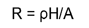
silicon substrate 1. Advantageously, the parameter H/A can be chosen by the manufacturer of an interposer according to the invention. Therefore, the electrical resistance of a through silicon via according to the invention may be easily adapted depending on the application of the through silicon via. - The isolation between the via 11 or 12 and the external portion of silicon of the doped
silicon substrate 1 is performed by surroundingtrenches 7. Said surroundingtrenches 7 are, at least, partially filled with an isolating material. Preferably the isolating material is a thermal silicon oxide and/or other dielectric. Preferably, thetrenches 7 are further completely filled with a dielectric. For example thetrenches 7 are filled by conformal deposition of alpha silicon or polysilicon or other insulating material. Preferably, the depth of said surroundingtrenches 7 is in the range of 200 to 700 µm, for example 200 to 300 µm. Preferably, the isolation between the two throughsilicon vias oxide layer 3 deposited on the top side of theepitaxial layer 2 and anoxide layer 31 deposited on the bottom side of the dopedsilicon substrate 1. - Each of the said through
silicon vias first electrodes second electrodes silicon substrate 1. - Therefore, the through
silicon vias silicon substrate 1. Advantageously, said throughsilicon vias silicon substrate 1 and theepitaxial layer 2. - The through
silicon vias diodes 35 integrated in theepitaxial layer 2 disposed back to back and forming a back-to-back diode. Each of the saiddiodes 35 is connected to the adjacenttop electrode - The
diodes 35 comprise a portion of theepitaxial layer 25 which is doped with a different type of dopant than the dopedsilicon substrate 1. For example, the doped silicon substrate is doped with N-type dopants and theepitaxial portions 25 are doped with P-type dopants, and thediodes 35 are PN silicon diodes. Advantageously, saiddiodes 35 are highly integrated in the silicon submount whatever the level of breakdown voltage of thesediodes 35. - The isolation between the two back to back diodes is performed by a
diode trench 6. Saiddiode trench 6 is, at least, partially filled with an isolating material. Preferably the isolating material is a thermal silicon oxide and/or other dielectric. Preferably, thetrench 6 is further completely filled with a dielectric. For example thetrench 6 is filled by conformal deposition of alpha silicon or polysilicon or other insulating material. Preferably, the depth of saiddiode trench 6 is in the range of 1 to 20 µm. More preferably, the diode trench is of a depth at least that of the epitaxial layer thereby protecting the continuity of the electric connection between the diodes. Preferably, the thickness of saiddiode trench 6 is in the range of 0.8 to 1 µm. - The interposer also comprises a
passivation layer 9 situated between the twotop electrodes passivation layer 9 insures that the two top electrodes are connected each other only by thediodes 35. - The
portions 24, of theepitaxial layer 2, being included in the throughsilicon vias silicon substrate 1. For example, if the dopedsilicon substrate 1 is doped with N-type dopant, theepitaxial portions 24 are also doped with N-type dopants. In an embodiment of the invention, the concentration of dopant in theportions 24 of the epitaxial layer is higher than the concentration if dopant in thesilicon substrate 1. For example in theportions 24 the concentration of dopant is in a range of 1017 to 1020 atoms per cubic centimetres. Advantageously, the dopedportion 24 of a through silicon via 11 or 12 insure a deep well electrical contact with thetop electrode vias - The peripheral insulation of the back-to-back diode facilitates the use of higher doping rates for the epitaxial layer at equivalent Zener tension allowing increased doping of the base of the parasitic bipolar transistor and consequently reducing its gain. The use of an isolation trench between the diodes extends the effective length of the base of the parasitic transistor, reducing its gain. For example, the combination of a higher doping rate and longer insulation trench lowers the gain of transistors to a value of less than one, making the system immune to the conduction trigger of the parasitic bipolar transistor.
- The
top electrodes silicon substrate 1 that constitute a through silicon via 11 or 12 and on the adjacent dopedportion 25 of theepitaxial layer 2. For example, the top electrodes are made of aluminium or copper. In an embodiment of the invention, the first metallic layer is plated with gold alloy, for example TiNiAu or TiPtAu. Thebottom electrodes top electrode electrodes - The interposer also comprises a
passivation layer 9 situated between the twotop electrodes passivation layer 9 insures that the two top electrodes 102 are connected each other only by thediodes 35. - Referring to
figures 2 , an exemplary embodiment of a manufacturing method according to the invention for an interposer as shown infigure 1 is described in detail. - As illustrated on
figure 2A , asilicon substrate 1 highly doped for example with N type dopant, for example Arsenic or Antimony or Phosphorus, is provided. For example, the concentration of dopants is in a range of 1017 to 1020 atoms per cubic centimetres. The resistivity of thesilicon substrate 1 can be adjusted, depending on the dopant concentration. In the first step A, anepitaxial layer 2 is deposited on top of thesilicon substrate 1. The thickness and the resistivity of saidepitaxial layer 2 may be chosen according to the desired electrical characteristics of thediodes 35. The first step further comprises the growth of asilicon oxide layer 3 above theepitaxial layer 2. - As shown in
figure 2B , in this step two doped layers are implanted within theepitaxial layer 2. - In order to build in the
diodes 35, a P or N dopedlayer 5 is needed. For example, if thesilicon substrate 1 is doped with N dopants, it is necessary to deposit a P dopedlayer 5. - Then P or N doped layers 4 are deposited on the
epitaxial layer 2. If thesilicon substrate 1 is doped with N dopants, it is necessary to deposit a N doped layer 4. - According to an embodiment of the invention, the deposition of said
doped layers 4 and 5 is performed by implant or by vapour deposition. - As shown in
figure 2C , deep surroundingtrenches 7 are etched. These surroundingtrenches 7 are situated between saidlayers 4 and 5. In the embodiment of the invention presentedfigures 2 , the depth of the surroundingtrenches 7 is lower than the thickness of thesilicon substrate 1, but is greater or equal than the final thickness of the interposer. In another embodiment of the invention, the surroundingtrenches 7 may be etched all the way through the dopedsilicon substrate 1. The surroundingtrenches 7 define the volume of the dopedsilicon substrate 1 that will constitute the throughsilicon vias top electrodes bottom electrodes - In the interposer presented in
figure 1 , the through silicon vias are connected by a diode. During step C, anon-through trench 6 is etched. Preferably, saidtrench 6 separates the dopedlayer 5 in two subparts 51. Advantageously, these subparts 51 will provides thediodes 35 in a further step of the manufacturing process. Advantageously, thediode trench 6 will provide the isolation between the twodiodes 35 disposed back to back. In an embodiment of the invention, thediode trench 6 is smaller than the surroundingtrenches 7. For example, thediode trench 6 is less deep than the surroundingtrenches 7. For example, the depth of thetrench 6 is in the range of 1 to 20 µm, and the depth of the surroundingtrenches 7 is in the range of 200 to 700 µm, for example 200 to 300 µm. In an embodiment of the invention, the depth and the width of both types of trenches are substantially proportional. Preferably, the width of thetrenches - In step D, the interposer is treated in order to make diffuse the N dopants of the doped layers 4 and the P dopants of the doped
layer 5 deposited in step B. The diffusion of the dopants of thelayer 5 in the volume of theepitaxial layer 2 delimited by thediode trench 6 and thevias trenches 7 lead to thediodes 35. Thediodes 35 are constituted by the PN junction between the dopedsilicon substrate 1 and the said volume ofepitaxial layer 2 wherein the dopants of the dopedlayer 5 have diffused. The dopants of the layer 4 diffuse in theepitaxial layer 2 to giveconduction zones 24. Advantageously, saidconduction zones 24 allow deep well electrical contact between thesilicon substrate 1 and the top electrodes. In an embodiment of the invention, the dopants of the doped layer 4 can diffuse in thesilicon substrate 1 and are not construed in theepitaxial layer 2, as shown in figure 5D. - In step D, an oxidation of the
trenches trenches trenches 7 comprise bridges 13 as described above, said bridges 13 are also oxidized. Advantageously, the oxidation of the surroundingtrenches 7 and of the bridges 13, provide the electrical isolation of the throughsilicon vias silicon substrate 1 thanks to the oxidised bridges 13. Advantageously, theoxidised diode trench 6 provides isolation between thediodes 35. In an embodiment of the invention, the trenches are not fully filled with oxide during the trenches' oxidation step, and the trenches may be further filled with isolating material. For example, the trenches are filled by deposition of alpha silicon or of doped or undoped polysilicon. - As shown in
figure 2E , in step E, thetop oxide layer 3 is etched in the contact area, and the metallic layers of thetop electrodes top oxide layer 3 is etched by a wet etching process. In an embodiment of the invention, before the metallic layer deposition, silicides are performed where theoxide layer 3 have been removed. Advantageously, this decrease the contact resistance between theconduction zones 24 and the metallic layers of thetop electrodes metallic layers - In step F, a
passivation layer 9 is performed. In an embodiment of the invention, a second metallic layer may be deposited and patterned over the first metallic layer of thetop electrodes passivation layer 9 provides electrical isolation between thetop electrodes - In step G, the wafer is reported on a
hard carrier 14. The fixation of the wafer in thehard carrier 14 is made on the top side of the wafer. This advantageously eases the manufacturing process of the bottom face of the wafer. - As shown in
figure 2H , in step H the wafer is ground on its bottom side. For example, the wafer is ground in order to approximately give its final thickness to the interposer. In the embodiment of the invention depicted infigures 2C to 2G , the surroundingtrenches 7 are less deep than the dopedsilicon substrate 1, but the depth of said surroundingtrenches 7 is greater than the final thickness of the interposer. Consequently, after the grinding step H that possibly includes a step of stress release (for example by SF6 dry etching), the surroundingtrenches 7 extend all the way through the remaining dopedsilicon substrate 1. Consequently, the throughconduction vias 11 are now isolated from the external portion of the doped silicon substrate by the surroundingtrenches 7. - As depict in figure 21, an
oxide layer 31 is deposited on the bottom face of the wafer. Further, as in step E, thebottom oxide layer 31 is etched in the contact area, andmetallic layers bottom oxide layer 31 is etched. In an embodiment of the invention, before the metallic layer deposition, silicides are performed where thebottom oxide layer 31 have been removed. Advantageously, this decreases the contact resistance between the conduction throughvias bottom electrodes metallic layers metallic layers bottom electrodes - As shown in
Figure 2J , in step J the wafer is removed from thehard carrier 14 and a submount according to the invention, as described infigure 1 , is obtained. - The juxtaposition of the insulation well of the vias and the diode implementation zone makes it possible to delimit in a single operation the outside outline of the circuit, the vias and the diode implementation zone resulting in the electrical isolating of each of the areas.
- Referring to
Figures 3 , an exemplary embodiment of a planarization process according to the invention for an interposer as shown inFigure 1 is described in detail. - As illustrated in
figure 3A , a patterneddielectric insulation layer 30 is provided, for example of silicon oxide. For example, the thickness of the dielectric insulation layer is in the range of 0.4 to 1.5 µm. In an embodiment of the invention, the dielectric layer is 0.9 µm and a first mask is used to pattern the dielectric insulation layer. In the first step A, a first layer ofpure aluminium 31 is deposited on top of the silicon oxide layer. For example, the first layer ofaluminium 31 is of a depth in the same range as that of thedielectric layer 30. For example, the first and subsequent metallic layers are deposited such that a layer of uniform thickness results. - The first layer of
aluminium 31 is patterned such that a planarized surface as shown inFigure 3B is formed. The surface may haveconstruction recesses 33 in the zones where underlying contacts are opened through the dielectric layer. - As shown in
Figure 3C , a second layer ofpure aluminium 32 is deposited atop the planarized surface. For example, the thickness of the second layer ofaluminium 32 is in the range of 1 to 3 µm. The second layer ofaluminium 32 preserves the construction recesses 33 corresponding to the contacts in the dielectric layer, the recesses having a depth in the range of 0.4 to 1.5 µm. - In
Figure 3D , the second layer ofaluminium 32 is patterned, for example by a photolithography and etching process that can preserve the construction recesses 33 and trench delimitation. For example, after patterning, thestep 34 formed by the second layer of aluminium has a thickness substantially proportional to that of the dielectric layer; in an embodiment of the invention, the thickness is 1 µm. For example, the patterning of the second layer ofaluminium 32 may be time controlled. In an embodiment of the invention, a second mask is used for the etching of the second layer of aluminium that is the inverse of the first mask used in the patterning of the dielectric insulation layer. - As shown in
Figure 3E , a layer ofsilicon oxide 36 is formed and patterned such that the construction recesses 33 are maintained. - In a further embodiment of the present invention,
Figure 3F shows atitanium barrier layer 37 deposited so as to encapsulate thesecond layer 32 of aluminium. For example, thesecond aluminium layer 32 may be etched to a depth whereby the titanium barrier layer is reached. - This planarization process can be realised to create desired surface conditions for each level of interconnection.
- The planarization process creates a structure used as a base for LEDs with a planarity of the front face comprised between 0.1 µm and 1 µm. This planarity makes it possible to have a step of collective transfer corresponding to a wafer on wafer bonding by thermo-compression and allows every bump of the LED interposer to contact the facing LED substrate in a satisfactory way, and at least on the overall surface of a wafer. Further, the method of the present invention is suitable for use with a variety of conductive layers, including aluminium.
- The juxtaposition of the insulation well of the vias with the implementation zones of the diodes makes it possible to delimit in a single step of lithography the outside outline of the circuit, the vias and the diodes embedded between the vias and to isolate electrically these various elements one from the others in the periphery. The ratios of width of trenches are adjusted to allow increased speed of engraving of the surrounding trenches with respect to the diode trench. The single operation obtains a result consisting of two trenches cutting and isolating the vias that cross the silicon substrate having a typical depth of 200 to 700 µm. The insulating diode trench crosses the epitaxial layer only, to a depth in the range of 1 to 20 µm thereby protecting the continuity of the electrical connection between the diodes by the substratum.
- Although embodiments of the present disclosure have been described in detail, those skilled in the art should understand that they may make various changes, substitutions and alterations herein without departing from the spirit and scope of the present disclosure.
Claims (16)
- An interposer device comprising
a doped silicon substrate (1) having an epitaxial layer (24) on a first side and two through vias (11, 12) extending from the first side to a second side opposite to the first side of the doped silicon substrate, wherein each through via comprises a volume of doped silicon substrate delimited by a surrounding trench (7) extending from the first to the second side of the doped silicon substrate such that said surrounding trench is arranged so as to electrically isolate the doped silicon substrate surrounded by said trench;
first and second conductive layers (121, 122) laid respectively on first and second sides of the first through via so as to be electrically connected together;
third and fourth conductive layers (112, 111) laid respectively on surfaces of the second through via so as to be electrically connected together, the first (122) and third (112) conductive layers being connected together by means of a back-to-back diode (35) wherein the corresponding diodes are isolated by a diode trench (6) having a depth at least equal to that of the epitaxial layer (24). - The interposer device according to claim 1, wherein the ratio H/S is smaller or equal to 1, with H the average distance between the first and second side of the through via and S the average width of the through via.
- The interposer device according to any of claim 1 or 2, wherein the surrounding trench (7) is at least partially filled with an isolating material, said isolating material being preferably thermal silicon oxide and/or other dielectric, and the filling of the trench is completed by conformal deposition of alpha silicon or polysilicon or an insulating material.
- The interposer device according to any of the preceding claims, wherein the ratio H/e is greater or equal to 15, with H the average distance between the first and second side of the through via (11) and e the average thickness of the surrounding trench (7).
- The interposer device of claim 1, further comprising:a first layer of aluminium (31) formed selectively and between the regions of oxide layer on the first surface of the silicon substrate;a second layer of aluminium (32) formed on first aluminium and silicon oxide layers; anda further layer of silicon oxide (36),wherein said aluminium layers are formed prior to the conductive layers (111, 112, 121, 122).
- The interposer device of claim 1, wherein the surrounding trenches have a depth of 200-700 µm, preferably of 200-300 µm.
- The interposer device of claim 1 wherein the diode trench has a depth of 1 - 20 µm.
- A method of forming an interposer device according to any of claims 1 - 7, comprising:providing a doped silicon substrate (1) having an epitaxial layer with a doping different to that of the remaining silicon substrate;delimiting two through vias (11, 12) extending from a first to a second side of the doped silicon substrate, a diode implementation zone between the vias and a diode trench (6) delimiting first and second areas of the diode implementation zone (25);respectively isolating electrically each via, the first area and the second area of the diode implementation zone (25);laying first and second conductive layers respectively on first and second sides of the first through via so as to be electrically connected together; andlaying third and fourth conductive layers respectively on surfaces of the second through via so as to be electrically connected together;wherein the first and third conductive layers being connected by the diodes of the diode implementation zone.
- The method of claim 8, further comprising a planarization process applied to at least one side of the silicon substrate, the planarization process comprising the steps of:deposition of a dielectric insulation layer on a first metallic layer;patterning of contacts in the dielectric insulation layer;deposition of a first metallic layer on the dielectric insulation layer;patterning of the first metallic layer;deposition of a second metallic layer; andpatterning of the second metallic layer.
- The method of claims 8 or 9, wherein a barrier layer is deposed encapsulating the first and second conductive layers, wherein said barrier layer can be titanium based.
- The method of any one of claims 8 - 10, wherein the steps are repeated to construct second and/or subsequent levels of interconnection.
- The method of claims 8 or 9, wherein the dielectric insulation layer has a thickness of 0.4 to 1.5 µm.
- The method of claims 8 or 9, wherein the first and second conductive layers have a thickness of 1 to 3 µm.
- The method of claims 8 or 9, wherein the first and second conductive layers are formed by constructing recesses in the zones where underlying contacts are opened through the dielectric insulation layer.
- The method of claims 8 or 9, wherein patterning of contacts in the dielectric insulation layer is realised using a first mask and wherein patterning of the second metallic layer is realised using a second mask that is the inverse of the first mask.
- The method according to any one of claims 8 - 15, wherein the second metallic layer is etched to a depth whereby the barrier layer is exposed.
Priority Applications (6)
| Application Number | Priority Date | Filing Date | Title |
|---|---|---|---|
| EP11306634.4A EP2602818A1 (en) | 2011-12-09 | 2011-12-09 | An interposer device |
| US14/363,937 US9412681B2 (en) | 2011-12-09 | 2012-12-06 | Interposer device |
| CN201280067254.4A CN104160498B (en) | 2011-12-09 | 2012-12-06 | Interposer |
| JP2014545263A JP6180428B2 (en) | 2011-12-09 | 2012-12-06 | Interposer device |
| PCT/EP2012/074680 WO2013083714A1 (en) | 2011-12-09 | 2012-12-06 | An interposer device |
| EP12806380.7A EP2789010B1 (en) | 2011-12-09 | 2012-12-06 | An interposer device |
Applications Claiming Priority (1)
| Application Number | Priority Date | Filing Date | Title |
|---|---|---|---|
| EP11306634.4A EP2602818A1 (en) | 2011-12-09 | 2011-12-09 | An interposer device |
Publications (1)
| Publication Number | Publication Date |
|---|---|
| EP2602818A1 true EP2602818A1 (en) | 2013-06-12 |
Family
ID=47435896
Family Applications (2)
| Application Number | Title | Priority Date | Filing Date |
|---|---|---|---|
| EP11306634.4A Withdrawn EP2602818A1 (en) | 2011-12-09 | 2011-12-09 | An interposer device |
| EP12806380.7A Active EP2789010B1 (en) | 2011-12-09 | 2012-12-06 | An interposer device |
Family Applications After (1)
| Application Number | Title | Priority Date | Filing Date |
|---|---|---|---|
| EP12806380.7A Active EP2789010B1 (en) | 2011-12-09 | 2012-12-06 | An interposer device |
Country Status (5)
| Country | Link |
|---|---|
| US (1) | US9412681B2 (en) |
| EP (2) | EP2602818A1 (en) |
| JP (1) | JP6180428B2 (en) |
| CN (1) | CN104160498B (en) |
| WO (1) | WO2013083714A1 (en) |
Families Citing this family (8)
| Publication number | Priority date | Publication date | Assignee | Title |
|---|---|---|---|---|
| DE112016002190B4 (en) | 2015-05-15 | 2021-10-07 | Panasonic Intellectual Property Management Co., Ltd. | Interposer |
| WO2018040100A1 (en) | 2016-09-05 | 2018-03-08 | 飞昂通讯科技南通有限公司 | Anti-interference semiconductor device for optical transceiver |
| CN108054154B (en) * | 2017-12-15 | 2020-10-27 | 吉安品位环保科技有限公司 | TSV Breakout Board for System-in-Package |
| CN108054155B (en) * | 2017-12-15 | 2020-05-05 | 佛山金航向电子科技有限公司 | Through Silicon Via Interposer for 3D Integrated Circuit Packaging |
| CN108074923B (en) * | 2017-12-15 | 2019-12-20 | 唐山国芯晶源电子有限公司 | Antistatic device for system-in-package |
| US11398516B2 (en) * | 2019-08-29 | 2022-07-26 | Taiwan Semiconductor Manufacturing Company, Ltd. | Conductive contact for ion through-substrate via |
| DE102020101246B4 (en) | 2019-08-29 | 2025-03-27 | Taiwan Semiconductor Manufacturing Co. Ltd. | Substrate via with doped channel region and corresponding manufacturing process |
| KR102868587B1 (en) | 2023-12-13 | 2025-10-02 | 주식회사 아이에스시 | Test Socket |
Citations (8)
| Publication number | Priority date | Publication date | Assignee | Title |
|---|---|---|---|---|
| US5187119A (en) * | 1991-02-11 | 1993-02-16 | The Boeing Company | Multichip module and integrated circuit substrates having planarized patterned surfaces |
| DE19729156A1 (en) * | 1996-08-09 | 1998-02-12 | Lg Semicon Co Ltd | Semiconductor component wiring forming method |
| EP0974817A1 (en) | 1997-04-03 | 2000-01-26 | Yamatake Corporation | Circuit board and detector, and method for manufacturing the same |
| DE10205026C1 (en) * | 2002-02-07 | 2003-05-28 | Bosch Gmbh Robert | Semiconductor substrate used for vertical integration of integrated circuits comprises a first conductor strip on its front side, and a region formed by insulating trenches and electrically insulated from the substrate |
| US6670271B1 (en) * | 2002-01-17 | 2003-12-30 | Advanced Micro Devices, Inc. | Growing a dual damascene structure using a copper seed layer and a damascene resist structure |
| JP2008166705A (en) * | 2006-12-06 | 2008-07-17 | Denso Corp | Semiconductor device and manufacturing method thereof |
| EP2045840A2 (en) * | 2007-10-01 | 2009-04-08 | Shinko Electric Industries Co., Ltd. | Wiring board with guard ring |
| WO2009053912A1 (en) * | 2007-10-25 | 2009-04-30 | Nxp B.V. | Semiconductor device with improved esd protection |
Family Cites Families (7)
| Publication number | Priority date | Publication date | Assignee | Title |
|---|---|---|---|---|
| JPS57112027A (en) * | 1980-12-29 | 1982-07-12 | Fujitsu Ltd | Manufacture of semiconductor device |
| JP3418548B2 (en) * | 1997-04-03 | 2003-06-23 | 株式会社山武 | Circuit board and method of manufacturing the same |
| JP2003197854A (en) * | 2001-12-26 | 2003-07-11 | Nec Electronics Corp | Double-sided connection type semiconductor device, multistage stacked type semiconductor device, method for manufacturing the same, and electronic component equipped with the semiconductor device |
| JP2004342935A (en) * | 2003-05-16 | 2004-12-02 | Semiconductor Energy Lab Co Ltd | Method of manufacturing interconnect line, and method of manufacturing semiconductor device |
| JP2007067216A (en) * | 2005-08-31 | 2007-03-15 | Sanyo Electric Co Ltd | Semiconductor device and manufacturing method thereof, circuit board and manufacturing method thereof |
| JP5343245B2 (en) * | 2008-05-15 | 2013-11-13 | 新光電気工業株式会社 | Manufacturing method of silicon interposer |
| US9224702B2 (en) * | 2013-12-12 | 2015-12-29 | Amazing Microelectronic Corp. | Three-dimension (3D) integrated circuit (IC) package |
-
2011
- 2011-12-09 EP EP11306634.4A patent/EP2602818A1/en not_active Withdrawn
-
2012
- 2012-12-06 JP JP2014545263A patent/JP6180428B2/en active Active
- 2012-12-06 US US14/363,937 patent/US9412681B2/en active Active
- 2012-12-06 CN CN201280067254.4A patent/CN104160498B/en active Active
- 2012-12-06 WO PCT/EP2012/074680 patent/WO2013083714A1/en not_active Ceased
- 2012-12-06 EP EP12806380.7A patent/EP2789010B1/en active Active
Patent Citations (8)
| Publication number | Priority date | Publication date | Assignee | Title |
|---|---|---|---|---|
| US5187119A (en) * | 1991-02-11 | 1993-02-16 | The Boeing Company | Multichip module and integrated circuit substrates having planarized patterned surfaces |
| DE19729156A1 (en) * | 1996-08-09 | 1998-02-12 | Lg Semicon Co Ltd | Semiconductor component wiring forming method |
| EP0974817A1 (en) | 1997-04-03 | 2000-01-26 | Yamatake Corporation | Circuit board and detector, and method for manufacturing the same |
| US6670271B1 (en) * | 2002-01-17 | 2003-12-30 | Advanced Micro Devices, Inc. | Growing a dual damascene structure using a copper seed layer and a damascene resist structure |
| DE10205026C1 (en) * | 2002-02-07 | 2003-05-28 | Bosch Gmbh Robert | Semiconductor substrate used for vertical integration of integrated circuits comprises a first conductor strip on its front side, and a region formed by insulating trenches and electrically insulated from the substrate |
| JP2008166705A (en) * | 2006-12-06 | 2008-07-17 | Denso Corp | Semiconductor device and manufacturing method thereof |
| EP2045840A2 (en) * | 2007-10-01 | 2009-04-08 | Shinko Electric Industries Co., Ltd. | Wiring board with guard ring |
| WO2009053912A1 (en) * | 2007-10-25 | 2009-04-30 | Nxp B.V. | Semiconductor device with improved esd protection |
Also Published As
| Publication number | Publication date |
|---|---|
| EP2789010B1 (en) | 2020-03-11 |
| US20140299963A1 (en) | 2014-10-09 |
| WO2013083714A1 (en) | 2013-06-13 |
| CN104160498A (en) | 2014-11-19 |
| US9412681B2 (en) | 2016-08-09 |
| JP2015503239A (en) | 2015-01-29 |
| JP6180428B2 (en) | 2017-08-16 |
| EP2789010A1 (en) | 2014-10-15 |
| CN104160498B (en) | 2017-09-26 |
Similar Documents
| Publication | Publication Date | Title |
|---|---|---|
| EP2789010B1 (en) | An interposer device | |
| KR101974198B1 (en) | Semiconductor device and method for fabricating the same | |
| CN111508930B (en) | Through-holes and methods of forming them | |
| EP1146558B1 (en) | Semiconductor device with damascene wiring structure and method of its fabrication | |
| US7700405B2 (en) | Microelectronic assembly with improved isolation voltage performance and a method for forming the same | |
| US20200381424A1 (en) | Monolithic multi-channel diode array | |
| JP5998459B2 (en) | Semiconductor device, manufacturing method thereof, and electronic component | |
| US8810010B2 (en) | Semiconductor device and method for fabricating the same | |
| US20130249011A1 (en) | Integrated circuit (ic) having tsvs and stress compensating layer | |
| KR20070059989A (en) | Semiconductor device and manufacturing method thereof | |
| KR20170118203A (en) | Microelectronic assemblies formed using metal silicides and methods of making | |
| KR101264926B1 (en) | Method of manufacturing semiconductor device and semiconductor device | |
| EP3591696B1 (en) | A method for producing a through semiconductor via connection | |
| US12218034B2 (en) | Semiconductor structure and method for manufacturing semiconductor structure | |
| WO2023023052A1 (en) | Through wafer trench isolation | |
| KR102724489B1 (en) | A semiconductor device and process for making same | |
| US20040043532A1 (en) | Integrated chip diode | |
| US7732848B2 (en) | Power semiconductor device with improved heat dissipation | |
| TWI851427B (en) | Schottky diode element and method for manufacturing the same | |
| US20260047189A1 (en) | Semiconductor device and method of manufacturing the same | |
| KR100829789B1 (en) | Semiconductor device and manufacturing method thereof | |
| CN119767697A (en) | Schottky diode element and manufacturing method thereof |
Legal Events
| Date | Code | Title | Description |
|---|---|---|---|
| PUAI | Public reference made under article 153(3) epc to a published international application that has entered the european phase |
Free format text: ORIGINAL CODE: 0009012 |
|
| AK | Designated contracting states |
Kind code of ref document: A1 Designated state(s): AL AT BE BG CH CY CZ DE DK EE ES FI FR GB GR HR HU IE IS IT LI LT LU LV MC MK MT NL NO PL PT RO RS SE SI SK SM TR |
|
| AX | Request for extension of the european patent |
Extension state: BA ME |
|
| STAA | Information on the status of an ep patent application or granted ep patent |
Free format text: STATUS: THE APPLICATION IS DEEMED TO BE WITHDRAWN |
|
| 18D | Application deemed to be withdrawn |
Effective date: 20131213 |