EP2600525A2 - Wireless communication device and semiconductor package device having a power amplifier therefor - Google Patents
Wireless communication device and semiconductor package device having a power amplifier therefor Download PDFInfo
- Publication number
- EP2600525A2 EP2600525A2 EP20120194494 EP12194494A EP2600525A2 EP 2600525 A2 EP2600525 A2 EP 2600525A2 EP 20120194494 EP20120194494 EP 20120194494 EP 12194494 A EP12194494 A EP 12194494A EP 2600525 A2 EP2600525 A2 EP 2600525A2
- Authority
- EP
- European Patent Office
- Prior art keywords
- amplifier block
- semiconductor package
- elements
- amplifier
- package device
- Prior art date
- Legal status (The legal status is an assumption and is not a legal conclusion. Google has not performed a legal analysis and makes no representation as to the accuracy of the status listed.)
- Withdrawn
Links
Images


Classifications
-
- H—ELECTRICITY
- H10—SEMICONDUCTOR DEVICES; ELECTRIC SOLID-STATE DEVICES NOT OTHERWISE PROVIDED FOR
- H10W—GENERIC PACKAGES, INTERCONNECTIONS, CONNECTORS OR OTHER CONSTRUCTIONAL DETAILS OF DEVICES COVERED BY CLASS H10
- H10W44/00—Electrical arrangements for controlling or matching impedance
- H10W44/20—Electrical arrangements for controlling or matching impedance at high-frequency [HF] or radio frequency [RF]
-
- H—ELECTRICITY
- H03—ELECTRONIC CIRCUITRY
- H03F—AMPLIFIERS
- H03F3/00—Amplifiers with only discharge tubes or only semiconductor devices as amplifying elements
- H03F3/189—High-frequency amplifiers, e.g. radio frequency amplifiers
- H03F3/19—High-frequency amplifiers, e.g. radio frequency amplifiers with semiconductor devices only
- H03F3/193—High-frequency amplifiers, e.g. radio frequency amplifiers with semiconductor devices only with field-effect devices
-
- H—ELECTRICITY
- H03—ELECTRONIC CIRCUITRY
- H03F—AMPLIFIERS
- H03F3/00—Amplifiers with only discharge tubes or only semiconductor devices as amplifying elements
- H03F3/189—High-frequency amplifiers, e.g. radio frequency amplifiers
- H03F3/19—High-frequency amplifiers, e.g. radio frequency amplifiers with semiconductor devices only
- H03F3/195—High-frequency amplifiers, e.g. radio frequency amplifiers with semiconductor devices only in integrated circuits
-
- H—ELECTRICITY
- H03—ELECTRONIC CIRCUITRY
- H03F—AMPLIFIERS
- H03F3/00—Amplifiers with only discharge tubes or only semiconductor devices as amplifying elements
- H03F3/20—Power amplifiers, e.g. Class B amplifiers, Class C amplifiers
- H03F3/24—Power amplifiers, e.g. Class B amplifiers, Class C amplifiers of transmitter output stages
- H03F3/245—Power amplifiers, e.g. Class B amplifiers, Class C amplifiers of transmitter output stages with semiconductor devices only
-
- H—ELECTRICITY
- H03—ELECTRONIC CIRCUITRY
- H03F—AMPLIFIERS
- H03F3/00—Amplifiers with only discharge tubes or only semiconductor devices as amplifying elements
- H03F3/45—Differential amplifiers
- H03F3/45071—Differential amplifiers with semiconductor devices only
- H03F3/45076—Differential amplifiers with semiconductor devices only characterised by the way of implementation of the active amplifying circuit in the differential amplifier
- H03F3/45179—Differential amplifiers with semiconductor devices only characterised by the way of implementation of the active amplifying circuit in the differential amplifier using MOSFET transistors as the active amplifying circuit
-
- H—ELECTRICITY
- H10—SEMICONDUCTOR DEVICES; ELECTRIC SOLID-STATE DEVICES NOT OTHERWISE PROVIDED FOR
- H10W—GENERIC PACKAGES, INTERCONNECTIONS, CONNECTORS OR OTHER CONSTRUCTIONAL DETAILS OF DEVICES COVERED BY CLASS H10
- H10W44/00—Electrical arrangements for controlling or matching impedance
- H10W44/501—Inductive arrangements
-
- H—ELECTRICITY
- H03—ELECTRONIC CIRCUITRY
- H03F—AMPLIFIERS
- H03F2203/00—Indexing scheme relating to amplifiers with only discharge tubes or only semiconductor devices as amplifying elements covered by H03F3/00
- H03F2203/45—Indexing scheme relating to differential amplifiers
- H03F2203/45394—Indexing scheme relating to differential amplifiers the AAC of the dif amp comprising FETs whose sources are not coupled, i.e. the AAC being a pseudo-differential amplifier
-
- H—ELECTRICITY
- H10—SEMICONDUCTOR DEVICES; ELECTRIC SOLID-STATE DEVICES NOT OTHERWISE PROVIDED FOR
- H10W—GENERIC PACKAGES, INTERCONNECTIONS, CONNECTORS OR OTHER CONSTRUCTIONAL DETAILS OF DEVICES COVERED BY CLASS H10
- H10W44/00—Electrical arrangements for controlling or matching impedance
- H10W44/20—Electrical arrangements for controlling or matching impedance at high-frequency [HF] or radio frequency [RF]
- H10W44/203—Electrical connections
- H10W44/206—Wires
-
- H—ELECTRICITY
- H10—SEMICONDUCTOR DEVICES; ELECTRIC SOLID-STATE DEVICES NOT OTHERWISE PROVIDED FOR
- H10W—GENERIC PACKAGES, INTERCONNECTIONS, CONNECTORS OR OTHER CONSTRUCTIONAL DETAILS OF DEVICES COVERED BY CLASS H10
- H10W44/00—Electrical arrangements for controlling or matching impedance
- H10W44/20—Electrical arrangements for controlling or matching impedance at high-frequency [HF] or radio frequency [RF]
- H10W44/203—Electrical connections
- H10W44/216—Waveguides, e.g. strip lines
-
- H—ELECTRICITY
- H10—SEMICONDUCTOR DEVICES; ELECTRIC SOLID-STATE DEVICES NOT OTHERWISE PROVIDED FOR
- H10W—GENERIC PACKAGES, INTERCONNECTIONS, CONNECTORS OR OTHER CONSTRUCTIONAL DETAILS OF DEVICES COVERED BY CLASS H10
- H10W44/00—Electrical arrangements for controlling or matching impedance
- H10W44/20—Electrical arrangements for controlling or matching impedance at high-frequency [HF] or radio frequency [RF]
- H10W44/226—Electrical arrangements for controlling or matching impedance at high-frequency [HF] or radio frequency [RF] for HF amplifiers
- H10W44/234—Arrangements for impedance matching
-
- H—ELECTRICITY
- H10—SEMICONDUCTOR DEVICES; ELECTRIC SOLID-STATE DEVICES NOT OTHERWISE PROVIDED FOR
- H10W—GENERIC PACKAGES, INTERCONNECTIONS, CONNECTORS OR OTHER CONSTRUCTIONAL DETAILS OF DEVICES COVERED BY CLASS H10
- H10W72/00—Interconnections or connectors in packages
- H10W72/50—Bond wires
- H10W72/541—Dispositions of bond wires
- H10W72/5445—Dispositions of bond wires being orthogonal to a side surface of the chip, e.g. parallel arrangements
Definitions
- the field of this invention relates to radio frequency (RF) power amplifiers (PAs) and semiconductor package device therefor.
- the invention is applicable to, but not limited to, a semiconductor package device comprising two or more amplifier blocks.
- radio frequency (RF) power amplifiers PAs
- the instantaneous bandwidth, or video bandwidth as it is often referred to, is the maximum signal bandwidth that an amplifier is able to properly amplify a communication signal.
- GSM Global System for Mobile Communication
- 3GPP 3 rd Generation Partnership Project
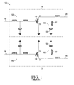
- FIG. 1 illustrates schematically a typical example of a RF PA circuit 100 comprising a first power amplifier block 110 and a second power amplifier block 120 operably coupled in parallel between inputs 102, 104 and outputs 170, 175 respectively, for example as may be used within RF integrated circuits (RFICs).
- Each power amplifier block 110, 120 comprises an input matching circuit 130, 140 operably coupling the respective RF input signal 102, 104 to a respective RF PA transistor 112, 122.
- the output of a drain port of each RF PA transistor 112, 122 is operably coupled to an output matching circuit 150, 160.
- the RF PA circuit 100 may be configured to operate as a push-pull (differential) amplifier, whereby inputs 102, 104 comprise differential inputs and the outputs 170, 175 comprise differential outputs. Equally, the RF PA circuit may be configured as a single ended amplifier circuit by operably coupling together the two inputs 102, 104 and the two outputs 170, 175 respectively.
- capacitors 155, 165 provide DC blocking for the respective shunt inductances 157, 167, whilst providing a short circuit for RF frequency signals such that the parallel reactance at such RF frequencies on the drain port of the respective transistor 112, 122 comprises an inductance.
- the capacitors 155, 165 comprise a capacitance value in the region of 200pF. Lower value capacitances are typically unsuitable since they cannot provide a good enough radio frequency (RF) short.
- capacitors 155, 165 limits the instantaneous bandwidth achievable, thus restricting the suitability of such an amplifier circuit for present and future RF PA drain modulation systems.
- lossy nature of the capacitors 155, 165 affects the peak efficiency of the amplifier circuit 100 (by a few percent).
- the single ended configuration is sensitive to ground connection inductance, which affects unit-to-unit (e.g. RF integrated circuit) RF performance dispersion.
- the present invention provides a semiconductor package device and a wireless communication device comprising such a semiconductor package device as described in the accompanying claims.
- Examples of the invention will be described with respect to an implementation of a radio frequency (RF) semiconductor package device, for example one that is suitable for use in a wireless communication unit, for example a cellular base station although the examples may readily be applied to a lower power PA design for, say, a subscriber wireless communication unit such as a mobile phone.
- RF radio frequency
- examples are described herein with respect to implementing, say, an 80W base station using laterally diffused metal oxide semiconductor (LDMOS) technology.
- Examples of the invention will also be described with respect to a semiconductor package device comprising two or more single ended amplifier blocks. However, it is envisaged that amplifier blocks other than single-ended amplifier blocks may be used in other examples.
- the term 'amplifier block' used hereinafter may encompass any other amplifier type.
- the term 'power transistor' used hereinafter may encompass any other power amplifier transistor, such as much lower power transistors, for example those suitable for use in mobile phone technology, where the output power may be of the order of, say 1W.
- examples of the invention are suitable in non-final PA stages, such as for use in pre-amplifier networks.
- examples of the invention may be implemented in any type of RF amplifier semiconductor device package. Examples of the invention may also be implemented with any type of RF transistor technology, such as Laterally Diffused Metal Oxide Semiconductor (LDMOS), gallium nitride (GaN), bipolar technology, etc.
- LDMOS Laterally Diffused Metal Oxide Semiconductor
- GaN gallium nitride
- bipolar technology etc.
- the semiconductor substrate described herein can be any semiconductor material or combinations of materials, such as gallium arsenide, silicon germanium, silicon-on-insulator (SOI), silicon, monocrystalline silicon, the like, and combinations of the above.
- SOI silicon-on-insulator
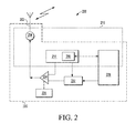
- FIG. 2 an example of a block diagram of a wireless communication unit 200 is illustrated that is capable of using a radio frequency (RF) power amplifier integrated circuit (PAIC) as hereinafter described with reference to some examples of the invention.
- RF radio frequency
- PAIC power amplifier integrated circuit
- the wireless communication unit 200 is shown as divided into two distinct portions - a receiver chain 210 (which will not be described for clarity purposes) and a transmitter chain 220.
- the wireless communication unit 200 contains an antenna coupled to an antenna switch 204 that provides signal control of RF signals in the wireless communication unit 200, as well as isolation between the receiver chain 210 and transmit chain 220.
- the antenna switch 204 may be replaced with a duplex filter, for frequency duplex communication units, as known to those skilled in the art.
- this essentially includes a signal processor 228, operably coupled to a modulation and up-converter circuit 222 and power amplifier (PA) module 224.
- a power source 226 is operably coupled to the PA module 224.
- the signal processor 228 and modulation and up-converter circuit 222 are operationally responsive to a controller 214.
- a timer 216 is operably coupled to the controller 214 to control the timing of operations, namely the transmission or reception of time-dependent signals.
- the power amplifier module 224 comprises a power amplifier integrated circuit (PAIC) being provided with a voltage source 226 and comprising a plurality of active components, for example power transistors, and associated RF matching components, for example as described in greater detail with respect to FIG. 3 .
- PAIC power amplifier integrated circuit
- a semiconductor package device comprising a first amplifier block, at least one further amplifier block and a differential inductance operably coupled between a plurality of elements of each of the outputs of the respective active components of the first amplifier block and the at least one further amplifier block.
- the differential inductance is arranged such that a substantially uniform inductance is provided between the elements of the first amplifier block and the elements of the at least one further amplifier block.
- the term 'uniform' related to inductance of the differential inductance is meant to encompass any substantially uniform inductance created between the elements of the first amplifier block and the elements of the at least one further amplifier block that facilitates the aims of the invention, within any reasonable manufacturing and design tolerance.
- non-uniform' as related to the configuration of successive, adjacent wire-bonding arrays, is meant to encompass any substantially non-uniform configuration that facilitates the aims of the invention in providing a substantially uniform inductance using substantially non-uniform wire-bonding lengths within any reasonable manufacturing and/or design tolerance.
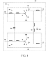
- the semiconductor package device 300 comprises a first amplifier block 310 and at least one further amplifier block 320, for example which form part of a Radio Frequency (RF) Power Amplifier (PA) device.
- the exemplary semiconductor package device described herein, and illustrated in the accompanying drawings comprises only two amplifier blocks for clarity purposes. Further amplifier blocks may also be operably coupled in parallel in further exemplary semiconductor package devices in the same manner.
- the amplifier blocks 310, 320 form part of a differential amplifier circuit 305, and as such are configured to operate as a push-pull (differential) amplifier. Accordingly, the amplifier blocks 310, 320, which individually comprise single ended amplifier blocks, are operably coupled in parallel between differential inputs 302, 304 and differential outputs 370, 375 of the differential amplifier circuit 305.
- Each of the first and at least one further amplifier blocks 310, 320 comprises an active component in the form of a respective power transistor 312, 322.
- the active component of each amplifier block 310, 320 comprises a field effect transistor in the form of a laterally diffused metal oxide semiconductor (LDMOS) power transistor 312, 322 comprising a gate terminal 316, 326 providing an input for the power transistor, a drain terminal 314, 324 providing an output for the power transistor, and a common source terminal 318, 328 operably coupled to ground.
- LDMOS laterally diffused metal oxide semiconductor
- each amplifier block 310, 320 is configured in accordance with a drain modulated amplifier system.
- the amplifier blocks 310, 320 each further comprise an input matching circuit 330, 340 operably coupled between respective inputs 302, 304 and the input (gate) 316, 326 of the respective power transistor 312, 322.
- the input matching circuits 330, 340 are operably coupled to one another via capacitance 335.
- all shunt elements are replaced by differential elements, for example the input shunt capacitors in the prior art parallel single-ended amplifier shown in FIG. 1 are replaced by a single input shunt capacitor in the push-pull (sometimes referred to as differential) amplifier shown in FIG. 3 .
- the amplifier blocks 310, 320 further comprise output matching circuits operably coupled together using a differential inductance 360 operably coupled between the outputs (drains) 314, 324 of the transistors 312, 322.
- FIG. 3 also illustrates a mid-point of the differential inductance 360 being operably coupled to a virtual ground 365.
- the amplifier blocks 310, 320 of FIG. 3 may be formed on a single die within the respective semiconductor package devices 300. Alternatively, the amplifier blocks 310, 320 may be formed on separate dies within the semiconductor package device 300.
- the differential inductance 360 is operably coupled between the outputs (drains) 314, 324 of the transistors 312, 322.
- Ports of high power devices, such as power transistors 312, 322 typical comprise an array of elements, or fingers, often numbering in the hundreds.
- the output (drain) 314, 424 of each of the power transistors 312, 322 comprises a plurality of elements 490, 495, to which the differential inductance 360 of FIG. 3 is operably coupled.
- the differential inductance comprises a first non-uniform wire-bonding array 420 operably coupled to the plurality of elements 490 of the output 314 of the transistor 312.
- the differential inductance further comprises at least one further non-uniform wire-bonding array 430 operably coupled to the plurality of elements 495 of the output 324 of the transistor 322.
- the differential inductance illustrated in FIG. 4 further comprises a microstrip line 410, for example in a form of a simple printed line on a substrate of the semiconductor package device 300 of FIG. 3 .
- the microstrip line 410 is operably coupled to the plurality of elements 490, 495 of the outputs 314, 324 of the respective active components 312, 322 by way of the non-uniform wire-bonding arrays 420, 430.
- the elements 490 of the output 314 of active component 312 are operably coupled to the elements 495 of the output 324 of active component 322 via the microstrip line 410 and wire-bonding arrays 420, 430.
- the non-uniform wire-bonding arrays are arranged, in conjunction with the microstrip line 410 for the illustrated example, such that a substantially uniform inductance is provided between the elements 490 of the first amplifier block 310 and the elements 495 of the at least one further amplifier block 320.
- a substantially uniform inductance is provided between the elements 490 of the first amplifier block 310 and the elements 495 of the at least one further amplifier block 320.
- the differential inductance 360 is illustrated, with only two bonding wires for each of the wire-bonding arrays 420, 430 being illustrated for clarity.
- the microstrip line 410 is operably coupled to the plurality of elements 490 and 495 of the outputs 314, 324 of the respective active components 312, 322 by way of the non-uniform wire-bonding arrays 420, 430.
- a first bonding wire 520 of the wire-bonding array 420 of FIG.4 is operably coupled between the output 314 of active component 312 and a point proximate a first end 510 of the microstrip line 410
- a second bonding wire 525 of the wire-bonding array 420 is operably coupled between the output 314 of active component 312 and a point located generally between the first end 510 of the microstrip line 410 and a central point 550 thereof.
- a second bonding wire 535 of the wire-bonding array 430 of FIG. 4 is operably coupled between the output 324 of active component 314 and a point located generally between the second end 515 of the microstrip 410 and the central point 550 thereof.
- each bonding wire 520, 525, 530, 535 is configured in accordance with a distance between the point at which that bonding wire 520, 525, 530, 535 is operably coupled to the microstrip line 410 and a common point thereof, for example the central point 550, such that a uniform inductance is achieved between the output 314, 324 of the respective active component 312, 322 and that common point via each bonding wire within the respective wire-bonding array 420, 430 of FIG. 4 .
- a substantially uniform inductance may be provided between the output 314 of active component 312 and the output 324 of active component 322 through all bonding wire paths there between.
- the inductance within the microstrip 410 between the respective points at which bonding wires 520 and 530 are operably coupled and the central point 550 may comprise, in this example, 172.5pH.
- the lengths of bonding wires 520, 530 may be arranged such that each bonding wire comprises an inductance of approximately 100pH, giving a total combined inductance for that path of 545pH (2*(172.5+100).
- the inductance within the microstrip 410 between the respective points at which bonding wires 525 and 535 are operably coupled and the central point 550 may comprise 32.5pH.
- each bonding wire comprises an inductance of approximately 240pH, also giving a total combined inductance for that path of 545pH (2*(32.5+240).
- the virtual ground 365 may be created substantially at the central point 550.
- the differential inductance such that a substantially uniform inductance is provided between the elements of the first amplifier block and the elements of the at least one further amplifier block, a proper power combination may be achieved between the active elements through the differential inductance.
- the output matching circuits for the amplifier blocks, which are provided by the differential inductance 360 are advantageously free from capacitances. As a result, an instantaneous bandwidth exceeding 100MHz is achievable (compared to 30MHz for the prior art design).
- a large value capacitor may be used to de-couple the output of the transistors to ground, as illustrated in FIG. 9 .
- the power amplifier semiconductor device package may be applied to other frequencies, for example 1 GHz or above power amplifier designs. In such higher frequency examples, the non-uniform wire-bonding may be replaced using ribbon technology.
- the power amplifier semiconductor device package may be applied to higher or lower output powers, for example 1W power amplifier designs instead of 10W designs, where there may be a higher contribution of microstrip lines.
- the achieving of some form of inductance may utilise other forms of routing radio frequency signals, such as a meandering transmission line of any shape or general direction.
- the non-uniform wire-bonding may be replaced or supplemented with a ball-grid array, for example using printed transmission lines. The absence of capacitances within the output matching circuits may enable an improvement in the peak power efficiency to be achieved.
- FIG. 7 there is illustrated four graphs 710, 720, 730, 740 showing RF performance of the aforementioned examples of an RF power amplifier such as the power amplifier arrangement illustrated in FIG. 3 .
- the graphs of FIG. 7 show input matching return loss (RL) 710, output power at 1dB compression (POUT) 720, small signal gain at 1dB compression 730 and Power Added Efficiency (PAE) 740 over a frequency bandwidth of 600MHz.
- RL input matching return loss
- POUT output power at 1dB compression
- PAE Power Added Efficiency
- FIG. 8 there is illustrated a graph 800 showing an example of video bandwidth capability for the aforementioned examples of an RF power amplifier arrangement, such as the power amplifier arrangement illustrated in FIG. 3 .
- the graph 800 illustrates an example of the performance of a single ended configuration 810 of such a power amplifier arrangement and an example of the performance of a differential (push-pull) configuration 820 of such a power amplifier arrangement.
- graph 900 showing an example of video bandwidth for the aforementioned examples of an RF power amplifier arrangement, such as the power amplifier arrangement illustrated in FIG. 3 .
- the graph 900 shows an example of video bandwidth for such an RF amplifier arrangement wherein the virtual ground 365 of the differential inductance is decoupled by way of a large value capacitance, for example as illustrated in FIG. 7 .
- graph 900 illustrates an advantage of decoupling the virtual ground 365 in terms of improving the insensitivity to ground connection inductance resulting from the differential inductance 360.
- connections may be any type of connection suitable to transfer signals from or to the respective nodes, units or devices, for example via intermediate devices. Accordingly, unless implied or stated otherwise the connections may for example be direct connections or indirect connections.
- the semiconductor substrate described herein can be any semiconductor material or combinations of materials, such as gallium arsenide, silicon germanium, silicon-on-insulator (SOI), silicon, monocrystalline silicon, the like, and combinations of the above.
- SOI silicon-on-insulator
- the conductors as discussed herein may be illustrated or described in reference to being a single conductor, a plurality of conductors, unidirectional conductors, or bidirectional conductors. However, different examples may vary the implementation of the conductors. For example, separate unidirectional conductors may be used rather than bidirectional conductors and vice versa. Also, plurality of conductors may be replaced with a single conductor that transfers multiple signals serially or in a time multiplexed manner. Likewise, single conductors carrying multiple signals may be separated out into various different conductors carrying subsets of these signals. Therefore, many options exist for transferring signals.
- any two components herein combined to achieve a particular functionality can be seen as “associated with” each other such that the desired functionality is achieved, irrespective of architectures or intermediary components.
- any two components so associated can also be viewed as being “operably connected,” or “operably coupled,” to each other to achieve the desired functionality.
- the illustrated amplifier blocks 310, 320 of FIG. 3 are located on a single integrated circuit or within a same device.
- amplifier blocks 310, 320 may include any number of separate integrated circuits or separate devices interconnected with each other.
- other modifications, variations and alternatives are also possible.
- the specifications and drawings are, accordingly, to be regarded in an illustrative rather than in a restrictive sense.
- any reference signs placed between parentheses shall not be construed as limiting the claim.
- the word 'comprising' does not exclude the presence of other elements or steps then those listed in a claim.
- the terms "a” or "an,” as used herein, are defined as one or more than one.
Landscapes
- Engineering & Computer Science (AREA)
- Power Engineering (AREA)
- Microelectronics & Electronic Packaging (AREA)
- Amplifiers (AREA)
Abstract
Description
- The field of this invention relates to radio frequency (RF) power amplifiers (PAs) and semiconductor package device therefor. The invention is applicable to, but not limited to, a semiconductor package device comprising two or more amplifier blocks.
- In the field of wireless communication, for many applications, such as within a cellular radio infrastructure, radio frequency (RF) power amplifiers (PAs) are continuously being required to support increasingly greater instantaneous bandwidths. The instantaneous bandwidth, or video bandwidth as it is often referred to, is the maximum signal bandwidth that an amplifier is able to properly amplify a communication signal. In particular, the progressive generations of wireless communication standards, such as the Global System for Mobile Communication (GSM) standard and the more recent 3rd Generation Partnership Project (3GPP) standard, have successively required increased bit rates. Accordingly, each generation has required an increased instantaneous bandwidth, and the future generations being considered are requiring that these bit rates are extended even further.
-
FIG. 1 illustrates schematically a typical example of aRF PA circuit 100 comprising a firstpower amplifier block 110 and a secondpower amplifier block 120 operably coupled in parallel betweeninputs outputs power amplifier block input matching circuit RF input signal RF PA transistor RF PA transistor output matching circuit RF PA circuit 100 may be configured to operate as a push-pull (differential) amplifier, wherebyinputs outputs inputs outputs - A problem with this known RF PA design, in either the differential configuration or the single ended configuration, is that the instantaneous bandwidth is limited by
capacitors output matching circuits Capacitors respective shunt inductances respective transistor capacitors capacitors capacitors - The present invention provides a semiconductor package device and a wireless communication device comprising such a semiconductor package device as described in the accompanying claims.
- Specific embodiments of the invention are set forth in the dependent claims.
- These and other aspects of the invention will be apparent from and elucidated with reference to the embodiments described hereinafter.
- Further details, aspects and examples of the invention will be described, by way of example only, with reference to the drawings. Elements in the figures are illustrated for simplicity and clarity and have not necessarily been drawn to scale.
-
FIG. 1 illustrates a known RF PA circuit. -
FIG. 2 illustrates an example of a block diagram of a wireless communication unit. -
FIG. 3 illustrates an example of a semiconductor package device. - FIG's 4 to 6 illustrate an example of a true high power differential power amplifier.
-
FIG. 7 illustrates examples of graphs showing RF performance of an RF PA arrangement. - FIG's 8 and 9 illustrate examples of graphs showing video bandwidth capability of RF PA arrangements.
- Examples of the invention will be described with respect to an implementation of a radio frequency (RF) semiconductor package device, for example one that is suitable for use in a wireless communication unit, for example a cellular base station although the examples may readily be applied to a lower power PA design for, say, a subscriber wireless communication unit such as a mobile phone. In this manner, examples are described herein with respect to implementing, say, an 80W base station using laterally diffused metal oxide semiconductor (LDMOS) technology. Examples of the invention will also be described with respect to a semiconductor package device comprising two or more single ended amplifier blocks. However, it is envisaged that amplifier blocks other than single-ended amplifier blocks may be used in other examples. Thus, the term 'amplifier block' used hereinafter may encompass any other amplifier type. In addition, the term 'power transistor' used hereinafter may encompass any other power amplifier transistor, such as much lower power transistors, for example those suitable for use in mobile phone technology, where the output power may be of the order of, say 1W. Furthermore, examples of the invention are suitable in non-final PA stages, such as for use in pre-amplifier networks. In addition, examples of the invention may be implemented in any type of RF amplifier semiconductor device package. Examples of the invention may also be implemented with any type of RF transistor technology, such as Laterally Diffused Metal Oxide Semiconductor (LDMOS), gallium nitride (GaN), bipolar technology, etc.
- The semiconductor substrate described herein can be any semiconductor material or combinations of materials, such as gallium arsenide, silicon germanium, silicon-on-insulator (SOI), silicon, monocrystalline silicon, the like, and combinations of the above.
- Referring now to
FIG. 2 , an example of a block diagram of awireless communication unit 200 is illustrated that is capable of using a radio frequency (RF) power amplifier integrated circuit (PAIC) as hereinafter described with reference to some examples of the invention. For the sake of clarity, thewireless communication unit 200 is shown as divided into two distinct portions - a receiver chain 210 (which will not be described for clarity purposes) and atransmitter chain 220. Thewireless communication unit 200 contains an antenna coupled to anantenna switch 204 that provides signal control of RF signals in thewireless communication unit 200, as well as isolation between thereceiver chain 210 andtransmit chain 220. Theantenna switch 204 may be replaced with a duplex filter, for frequency duplex communication units, as known to those skilled in the art. - With regard to the
transmit chain 220, this essentially includes asignal processor 228, operably coupled to a modulation and up-converter circuit 222 and power amplifier (PA)module 224. Apower source 226 is operably coupled to thePA module 224. Thesignal processor 228 and modulation and up-converter circuit 222 are operationally responsive to acontroller 214. Atimer 216 is operably coupled to thecontroller 214 to control the timing of operations, namely the transmission or reception of time-dependent signals. Thepower amplifier module 224 comprises a power amplifier integrated circuit (PAIC) being provided with avoltage source 226 and comprising a plurality of active components, for example power transistors, and associated RF matching components, for example as described in greater detail with respect toFIG. 3 . - In summary, in one example there is provided a semiconductor package device comprising a first amplifier block, at least one further amplifier block and a differential inductance operably coupled between a plurality of elements of each of the outputs of the respective active components of the first amplifier block and the at least one further amplifier block. The differential inductance is arranged such that a substantially uniform inductance is provided between the elements of the first amplifier block and the elements of the at least one further amplifier block. Hereinafter, the term 'uniform' related to inductance of the differential inductance, is meant to encompass any substantially uniform inductance created between the elements of the first amplifier block and the elements of the at least one further amplifier block that facilitates the aims of the invention, within any reasonable manufacturing and design tolerance. Similarly, and hereinafter, the term 'non-uniform' as related to the configuration of successive, adjacent wire-bonding arrays, is meant to encompass any substantially non-uniform configuration that facilitates the aims of the invention in providing a substantially uniform inductance using substantially non-uniform wire-bonding lengths within any reasonable manufacturing and/or design tolerance.
- Referring now to
FIG. 3 there is illustrated an example of such asemiconductor package device 300, for example in a form of a power amplifier integrated circuit (PAIC) or the like. Thesemiconductor package device 300 comprises afirst amplifier block 310 and at least onefurther amplifier block 320, for example which form part of a Radio Frequency (RF) Power Amplifier (PA) device. The exemplary semiconductor package device described herein, and illustrated in the accompanying drawings, comprises only two amplifier blocks for clarity purposes. Further amplifier blocks may also be operably coupled in parallel in further exemplary semiconductor package devices in the same manner. For the example illustrated inFIG. 3 , theamplifier blocks differential amplifier circuit 305, and as such are configured to operate as a push-pull (differential) amplifier. Accordingly, theamplifier blocks differential inputs differential outputs differential amplifier circuit 305. - Each of the first and at least one
further amplifier blocks respective power transistor amplifier block power transistor gate terminal drain terminal common source terminal amplifier block input matching circuit respective inputs respective power transistor input matching circuits capacitance 335. Thus, all shunt elements are replaced by differential elements, for example the input shunt capacitors in the prior art parallel single-ended amplifier shown inFIG. 1 are replaced by a single input shunt capacitor in the push-pull (sometimes referred to as differential) amplifier shown inFIG. 3 . The amplifier blocks 310, 320 further comprise output matching circuits operably coupled together using adifferential inductance 360 operably coupled between the outputs (drains) 314, 324 of thetransistors FIG. 3 also illustrates a mid-point of thedifferential inductance 360 being operably coupled to avirtual ground 365. - The amplifier blocks 310, 320 of
FIG. 3 may be formed on a single die within the respectivesemiconductor package devices 300. Alternatively, the amplifier blocks 310, 320 may be formed on separate dies within thesemiconductor package device 300. - Referring now to
FIG. 4 , there is illustrated an example of thedifferential inductance 360 ofFIG. 3 . As previously mentioned, thedifferential inductance 360 is operably coupled between the outputs (drains) 314, 324 of thetransistors power transistors FIG. 4 , the output (drain) 314, 424 of each of thepower transistors elements differential inductance 360 ofFIG. 3 is operably coupled. For the illustrated example, the differential inductance comprises a first non-uniform wire-bonding array 420 operably coupled to the plurality ofelements 490 of theoutput 314 of thetransistor 312. The differential inductance further comprises at least one further non-uniform wire-bonding array 430 operably coupled to the plurality ofelements 495 of theoutput 324 of thetransistor 322. The differential inductance illustrated inFIG. 4 further comprises amicrostrip line 410, for example in a form of a simple printed line on a substrate of thesemiconductor package device 300 ofFIG. 3 . Themicrostrip line 410 is operably coupled to the plurality ofelements outputs active components bonding arrays elements 490 of theoutput 314 ofactive component 312 are operably coupled to theelements 495 of theoutput 324 ofactive component 322 via themicrostrip line 410 and wire-bonding arrays - The non-uniform wire-bonding arrays are arranged, in conjunction with the
microstrip line 410 for the illustrated example, such that a substantially uniform inductance is provided between theelements 490 of thefirst amplifier block 310 and theelements 495 of the at least onefurther amplifier block 320. For example, referring toFIG. 5 and FIG. 6 thedifferential inductance 360 is illustrated, with only two bonding wires for each of the wire-bonding arrays microstrip line 410 is operably coupled to the plurality ofelements outputs active components bonding arrays - Referring now to FIG's 5 and 6, a
first bonding wire 520 of the wire-bonding array 420 ofFIG.4 is operably coupled between theoutput 314 ofactive component 312 and a point proximate afirst end 510 of themicrostrip line 410, and asecond bonding wire 525 of the wire-bonding array 420 is operably coupled between theoutput 314 ofactive component 312 and a point located generally between thefirst end 510 of themicrostrip line 410 and acentral point 550 thereof. Similarly, afirst bonding wire 530 of the wire-bonding array 430 ofFIG. 4 is operably coupled between theoutput 324 ofactive component 322 and a point proximate asecond end 515 of themicrostrip line 410, and asecond bonding wire 535 of the wire-bonding array 430 ofFIG. 4 is operably coupled between theoutput 324 ofactive component 314 and a point located generally between thesecond end 515 of themicrostrip 410 and thecentral point 550 thereof. - For the illustrated example, the length of each
bonding wire bonding wire microstrip line 410 and a common point thereof, for example thecentral point 550, such that a uniform inductance is achieved between theoutput active component bonding array FIG. 4 . As a result, a substantially uniform inductance may be provided between theoutput 314 ofactive component 312 and theoutput 324 ofactive component 322 through all bonding wire paths there between. - For example, and as illustrated in
FIG. 6 , the inductance within themicrostrip 410 between the respective points at whichbonding wires central point 550 may comprise, in this example, 172.5pH. The lengths ofbonding wires microstrip 410 between the respective points at whichbonding wires central point 550 may comprise 32.5pH. Accordingly, the lengths ofbonding wires virtual ground 365 may be created substantially at thecentral point 550. - Thus, by arranging the differential inductance such that a substantially uniform inductance is provided between the elements of the first amplifier block and the elements of the at least one further amplifier block, a proper power combination may be achieved between the active elements through the differential inductance. In addition, the output matching circuits for the amplifier blocks, which are provided by the
differential inductance 360, are advantageously free from capacitances. As a result, an instantaneous bandwidth exceeding 100MHz is achievable (compared to 30MHz for the prior art design). - In one example implementation, a large value capacitor may be used to de-couple the output of the transistors to ground, as illustrated in
FIG. 9 . In yet another example, the power amplifier semiconductor device package may be applied to other frequencies, for example 1 GHz or above power amplifier designs. In such higher frequency examples, the non-uniform wire-bonding may be replaced using ribbon technology. - Furthermore, in another example, the power amplifier semiconductor device package may be applied to higher or lower output powers, for example 1W power amplifier designs instead of 10W designs, where there may be a higher contribution of microstrip lines. In addition, in another example, depending upon the frequency, required output power and physical dimensions of the power transistors, the achieving of some form of inductance may utilise other forms of routing radio frequency signals, such as a meandering transmission line of any shape or general direction. In other examples, the non-uniform wire-bonding may be replaced or supplemented with a ball-grid array, for example using printed transmission lines. The absence of capacitances within the output matching circuits may enable an improvement in the peak power efficiency to be achieved.
- Referring now to
FIG. 7 , there is illustrated fourgraphs FIG. 3 . The graphs ofFIG. 7 show input matching return loss (RL) 710, output power at 1dB compression (POUT) 720, small signal gain at1dB compression 730 and Power Added Efficiency (PAE) 740 over a frequency bandwidth of 600MHz. This is in contrast to conventional RF power amplifier arrangements, which are only capable of achieving similar performance characteristics over a much narrower frequency bandwidth of around 60MHz. - Referring now to
FIG. 8 , there is illustrated agraph 800 showing an example of video bandwidth capability for the aforementioned examples of an RF power amplifier arrangement, such as the power amplifier arrangement illustrated inFIG. 3 . In particular, thegraph 800 illustrates an example of the performance of a single endedconfiguration 810 of such a power amplifier arrangement and an example of the performance of a differential (push-pull)configuration 820 of such a power amplifier arrangement. - Referring now to
FIG. 9 , there is illustrated agraph 900 showing an example of video bandwidth for the aforementioned examples of an RF power amplifier arrangement, such as the power amplifier arrangement illustrated inFIG. 3 . More particularly, thegraph 900 shows an example of video bandwidth for such an RF amplifier arrangement wherein thevirtual ground 365 of the differential inductance is decoupled by way of a large value capacitance, for example as illustrated inFIG. 7 . In this manner,graph 900 illustrates an advantage of decoupling thevirtual ground 365 in terms of improving the insensitivity to ground connection inductance resulting from thedifferential inductance 360. - In the foregoing specification, the invention has been described with reference to specific examples of embodiments of the invention. It will, however, be evident that various modifications and changes may be made therein without departing from the broader spirit and scope of the invention as set forth in the appended claims. For example, the connections may be any type of connection suitable to transfer signals from or to the respective nodes, units or devices, for example via intermediate devices. Accordingly, unless implied or stated otherwise the connections may for example be direct connections or indirect connections.
- The semiconductor substrate described herein can be any semiconductor material or combinations of materials, such as gallium arsenide, silicon germanium, silicon-on-insulator (SOI), silicon, monocrystalline silicon, the like, and combinations of the above.
- The conductors as discussed herein may be illustrated or described in reference to being a single conductor, a plurality of conductors, unidirectional conductors, or bidirectional conductors. However, different examples may vary the implementation of the conductors. For example, separate unidirectional conductors may be used rather than bidirectional conductors and vice versa. Also, plurality of conductors may be replaced with a single conductor that transfers multiple signals serially or in a time multiplexed manner. Likewise, single conductors carrying multiple signals may be separated out into various different conductors carrying subsets of these signals. Therefore, many options exist for transferring signals.
- Because the apparatus implementing the present invention is, for the most part, composed of electronic components and circuits known to those skilled in the art, circuit details will not be explained in any greater extent than that considered necessary as illustrated above, for the understanding and appreciation of the underlying concepts of the present invention and in order not to obfuscate or distract from the teachings of the present invention.
- Although the invention has been described with respect to specific conductivity types or polarity of potentials, skilled artisans appreciated that conductivity types and polarities of potentials may be reversed.
- Moreover, the terms "front," "back," "top," "bottom," "over," "under" and the like in the description and in the claims, if any, are used for descriptive purposes and not necessarily for describing permanent relative positions. It is understood that the terms so used are interchangeable under appropriate circumstances such that the examples of the invention described herein are, for example, capable of operation in other orientations than those illustrated or otherwise described herein.
- It is to be understood that the architectures depicted herein are merely exemplary, and that in fact many other architectures can be implemented which achieve the same functionality. In an abstract, but still definite sense, any arrangement of components to achieve the same functionality is effectively "associated" such that the desired functionality is achieved. Hence, any two components herein combined to achieve a particular functionality can be seen as "associated with" each other such that the desired functionality is achieved, irrespective of architectures or intermediary components. Likewise, any two components so associated can also be viewed as being "operably connected," or "operably coupled," to each other to achieve the desired functionality.
- Also for example, in one example, the illustrated amplifier blocks 310, 320 of
FIG. 3 are located on a single integrated circuit or within a same device. Alternatively, amplifier blocks 310, 320 may include any number of separate integrated circuits or separate devices interconnected with each other. Furthermore, other modifications, variations and alternatives are also possible. The specifications and drawings are, accordingly, to be regarded in an illustrative rather than in a restrictive sense. - In the claims, any reference signs placed between parentheses shall not be construed as limiting the claim. The word 'comprising' does not exclude the presence of other elements or steps then those listed in a claim. Furthermore, Furthermore, the terms "a" or "an," as used herein, are defined as one or more than one. Also, the use of introductory phrases such as "at least one" and "one or more" in the claims should not be construed to imply that the introduction of another claim element by the indefinite articles "a" or "an" limits any particular claim containing such introduced claim element to inventions containing only one such element, even when the same claim includes the introductory phrases "one or more" or "at least one" and indefinite articles such as "a" or "an." The same holds true for the use of definite articles. Unless stated otherwise, terms such as "first" and "second" are used to arbitrarily distinguish between the elements such terms describe. Thus, these terms are not necessarily intended to indicate temporal or other prioritization of such elements. The mere fact that certain measures are recited in mutually different claims does not indicate that a combination of these measures cannot be used to advantage.
Claims (11)
- A semiconductor package device (300) comprising a first amplifier block (310), at least one further amplifier block (320) and at least one differential inductance (360) operably coupled between a first plurality of elements (490) of an output (314) of a first active component (312) of the first amplifier block (310) and a second plurality of elements (495) of an output (324) of a second active component (322) of the at least one further amplifier block (320); wherein the differential inductance (360) is arranged such that a uniform inductance is provided between the first plurality of elements (490) of the first active component (314) of the first amplifier block (310) and the second plurality of elements (495) of the second active component (324) of the at least one further amplifier block (320).
- The semiconductor package device (300) of Claim 1 wherein the differential inductance (360) comprises a number of non-uniform wire-bonding arrays (420, 430) arranged such that a uniform inductance is provided between the first plurality of elements (490) of the first active component (314) of the first amplifier block (310) and the second plurality of elements (495) of the second active component (324) of the at least one further amplifier block (320).
- The semiconductor package device (300) of Claim 2 wherein the differential inductance (360) comprises a microstrip line (410), the microstrip line (410) being operably coupled to the first and second plurality of elements (490, 495) of the outputs (314, 324) of the respective first and second active components (312, 322) by way of the non-uniform wire-bonding arrays (420, 430).
- The semiconductor package device (300) of any preceding Claim wherein the first amplifier block (310) and the at least one further amplifier block (320) form part of a differential amplifier circuit (305), and are operably coupled in parallel between differential inputs (302, 304) and differential outputs (370, 375) of the differential amplifier circuit (305).
- The semiconductor package device (300) of any preceding Claim wherein the first amplifier block (310) and the at least one further amplifier block (320) each comprise a field effect transistor.
- The semiconductor package device (300) of any preceding Claim wherein the first amplifier block (310) and the at least one further amplifier block (320) are configured in accordance with a drain modulated amplifier system.
- The semiconductor package device (300) of any preceding Claim wherein the first amplifier block (310) and the at least one further amplifier block (320) each comprise a laterally diffused metal oxide semiconductor (LDMOS) device.
- The semiconductor package device (300) of any preceding Claim wherein the first amplifier block (310) and the at least one further amplifier block (320) form part of a Radio Frequency (RF) Power Amplifier (PA) device.
- The semiconductor package device (300) of any preceding Claim wherein the first amplifier block (310) and the at least one further amplifier block (320) are formed on a single die within the semiconductor package device (300).
- The semiconductor package device (300) of any of Claims 1 to 8 wherein the first amplifier block (310) and the at least one further amplifier block (320) are formed on separate dies within the semiconductor package device (300).
- A wireless communication device (200) comprising a first amplifier block (310), at least one further amplifier block (320), and at least one differential inductance (360) operably coupled between a first plurality of elements (490) of an output (314) of a first active component (312) of the first amplifier block (310) and a second plurality of elements (495) of an output (324) of a second active component (322) of the at least one further amplifier block (320); wherein the differential inductance (360) is arranged such that a uniform inductance is provided between the first plurality of elements (490) of the first active component (314) of the first amplifier block (310) and the second plurality of elements (495) of the second active component (324) of the at least one further amplifier block (320).
Priority Applications (1)
| Application Number | Priority Date | Filing Date | Title |
|---|---|---|---|
| EP20120194494 EP2600525A3 (en) | 2009-04-30 | 2009-04-30 | Wireless communication device and semiconductor package device having a power amplifier therefor |
Applications Claiming Priority (3)
| Application Number | Priority Date | Filing Date | Title |
|---|---|---|---|
| EP20120194494 EP2600525A3 (en) | 2009-04-30 | 2009-04-30 | Wireless communication device and semiconductor package device having a power amplifier therefor |
| IB200954335 | 2009-04-30 | ||
| EP20090787356 EP2425527B1 (en) | 2009-04-30 | 2009-04-30 | Wireless communication device and semiconductor package device having a power amplifier therefor |
Related Parent Applications (2)
| Application Number | Title | Priority Date | Filing Date |
|---|---|---|---|
| EP09787356.6 Division | 2009-04-30 | ||
| EP20090787356 Division EP2425527B1 (en) | 2009-04-30 | 2009-04-30 | Wireless communication device and semiconductor package device having a power amplifier therefor |
Publications (2)
| Publication Number | Publication Date |
|---|---|
| EP2600525A2 true EP2600525A2 (en) | 2013-06-05 |
| EP2600525A3 EP2600525A3 (en) | 2014-04-09 |
Family
ID=48183095
Family Applications (1)
| Application Number | Title | Priority Date | Filing Date |
|---|---|---|---|
| EP20120194494 Withdrawn EP2600525A3 (en) | 2009-04-30 | 2009-04-30 | Wireless communication device and semiconductor package device having a power amplifier therefor |
Country Status (1)
| Country | Link |
|---|---|
| EP (1) | EP2600525A3 (en) |
Cited By (1)
| Publication number | Priority date | Publication date | Assignee | Title |
|---|---|---|---|---|
| EP2838194A1 (en) * | 2013-08-14 | 2015-02-18 | Nxp B.V. | Amplifier circuits |
Family Cites Families (12)
| Publication number | Priority date | Publication date | Assignee | Title |
|---|---|---|---|---|
| US4193083A (en) * | 1977-01-07 | 1980-03-11 | Varian Associates, Inc. | Package for push-pull semiconductor devices |
| US5488252A (en) * | 1994-08-16 | 1996-01-30 | Telefonaktiebolaget L M Erricsson | Layout for radio frequency power transistors |
| US6177834B1 (en) * | 1998-12-02 | 2001-01-23 | Ericsson, Inc. | Output matched LDMOS power transistor device |
| US6670850B1 (en) * | 2002-06-13 | 2003-12-30 | Linear Technology Corp. | Ultra-wideband constant gain CMOS amplifier |
| US6734728B1 (en) * | 2002-12-19 | 2004-05-11 | Infineon Technologies North America Corp. | RF power transistor with internal bias feed |
| US6963247B2 (en) * | 2003-11-21 | 2005-11-08 | Nokia Corporation | Gain stabilization technique for narrow band integrated low noise amplifiers |
| US7145390B2 (en) * | 2004-09-03 | 2006-12-05 | Broadcom Corporation | Differential power amplifier and method in class AB mode |
| US20060050809A1 (en) * | 2004-09-03 | 2006-03-09 | Broadcom Corporation | System and method for reducing phase distortion in a linear transmitter via the introduction of bias currents to a power amplifier |
| KR20070116115A (en) * | 2005-03-18 | 2007-12-06 | 엔엑스피 비 브이 | Electronic RF device and its manufacturing method |
| US7224225B2 (en) * | 2005-04-26 | 2007-05-29 | Intel Corporation | Differential inductor based low noise amplifier |
| FI20055402A0 (en) * | 2005-07-11 | 2005-07-11 | Nokia Corp | Inductor for multi-band radio frequency operation |
| US7564303B2 (en) * | 2005-07-26 | 2009-07-21 | Infineon Technologies Ag | Semiconductor power device and RF signal amplifier |
-
2009
- 2009-04-30 EP EP20120194494 patent/EP2600525A3/en not_active Withdrawn
Non-Patent Citations (1)
| Title |
|---|
| None |
Cited By (4)
| Publication number | Priority date | Publication date | Assignee | Title |
|---|---|---|---|---|
| EP2838194A1 (en) * | 2013-08-14 | 2015-02-18 | Nxp B.V. | Amplifier circuits |
| CN104378072A (en) * | 2013-08-14 | 2015-02-25 | 恩智浦有限公司 | Amplifier circuits |
| US9041465B2 (en) | 2013-08-14 | 2015-05-26 | Nxp, B.V. | Amplifier circuits |
| CN104378072B (en) * | 2013-08-14 | 2017-08-11 | 安普林荷兰有限公司 | Amplifier circuit |
Also Published As
| Publication number | Publication date |
|---|---|
| EP2600525A3 (en) | 2014-04-09 |
Similar Documents
| Publication | Publication Date | Title |
|---|---|---|
| EP2425527B1 (en) | Wireless communication device and semiconductor package device having a power amplifier therefor | |
| US8253495B2 (en) | Wireless communication device and semiconductor package device having a power amplifier therefor | |
| US10903806B2 (en) | Radio frequency circuitr having an integrated harmonic filter and a radio frequency circuit having transistors of different threshold voltages | |
| US9041470B2 (en) | Wireless communication unit and semiconductor device having a power amplifier therefor | |
| US20170077877A1 (en) | Radio frequency circuitr having an integrated harmonic filter and a radio frequency circuit having transistors of different threshold voltages | |
| EP3247038A1 (en) | Multiple-path rf amplifiers with angularly offset signal path directions, and methods of manufacture thereof | |
| CN114374363A (en) | Doherty Power Amplifiers and Devices | |
| US20150295547A1 (en) | Amplification stage and wideband power amplifier | |
| CN113014211B (en) | Multistage power amplifiers and devices with low-voltage drive stages | |
| TWI632770B (en) | Transformer for monolithic microwave integrated circuits | |
| US12395171B2 (en) | Switch circuits with parallel transistor stacks and capacitor networks for balancing off-state RF voltages, and methods of their operation | |
| US9503030B2 (en) | Radio frequency power amplifier | |
| CN103368601A (en) | Front end of wireless communication transceiver | |
| CN1407828A (en) | High-frequency circuit device and mobile communication device | |
| US11418190B2 (en) | Switch circuits and transistor stacks with capacitor networks for balancing off-state RF voltages and methods of their operation | |
| CN114070288A (en) | Switching circuit with parallel transistor stack and method of operation thereof | |
| EP2600525A2 (en) | Wireless communication device and semiconductor package device having a power amplifier therefor | |
| US10756727B2 (en) | Switching circuit and high-frequency module | |
| CN102891700B (en) | RF antenna switch circuit, high frequency antenna component and mobile communication device | |
| US12512792B2 (en) | Radio frequency amplifier | |
| US20230040780A1 (en) | Class inverse f doherty amplifier | |
| US20190028074A1 (en) | Communication unit | |
| US20250309928A1 (en) | Radio frequency switch isolation techniques, systems, and methods | |
| CN121749910A (en) | Doherty power amplifier with harmonic frequency resonant circuit | |
| CN103326737B (en) | Digital wireless communication transceiver module |
Legal Events
| Date | Code | Title | Description |
|---|---|---|---|
| PUAI | Public reference made under article 153(3) epc to a published international application that has entered the european phase |
Free format text: ORIGINAL CODE: 0009012 |
|
| AC | Divisional application: reference to earlier application |
Ref document number: 2425527 Country of ref document: EP Kind code of ref document: P |
|
| AK | Designated contracting states |
Kind code of ref document: A2 Designated state(s): AT BE BG CH CY CZ DE DK EE ES FI FR GB GR HR HU IE IS IT LI LT LU LV MC MK MT NL NO PL PT RO SE SI SK TR |
|
| RIC1 | Information provided on ipc code assigned before grant |
Ipc: H03F 3/191 20060101ALI20131119BHEP Ipc: H03F 3/189 20060101AFI20131119BHEP |
|
| PUAL | Search report despatched |
Free format text: ORIGINAL CODE: 0009013 |
|
| AK | Designated contracting states |
Kind code of ref document: A3 Designated state(s): AT BE BG CH CY CZ DE DK EE ES FI FR GB GR HR HU IE IS IT LI LT LU LV MC MK MT NL NO PL PT RO SE SI SK TR |
|
| RIC1 | Information provided on ipc code assigned before grant |
Ipc: H03F 3/193 20060101ALI20140305BHEP Ipc: H03F 3/45 20060101ALI20140305BHEP Ipc: H03F 3/24 20060101ALI20140305BHEP Ipc: H01L 23/64 20060101ALI20140305BHEP Ipc: H03F 3/191 20060101ALI20140305BHEP Ipc: H01L 23/66 20060101ALI20140305BHEP Ipc: H03F 3/189 20060101AFI20140305BHEP Ipc: H03F 3/195 20060101ALI20140305BHEP |
|
| 17P | Request for examination filed |
Effective date: 20141009 |
|
| RBV | Designated contracting states (corrected) |
Designated state(s): AT BE BG CH CY CZ DE DK EE ES FI FR GB GR HR HU IE IS IT LI LT LU LV MC MK MT NL NO PL PT RO SE SI SK TR |
|
| 17Q | First examination report despatched |
Effective date: 20141113 |
|
| STAA | Information on the status of an ep patent application or granted ep patent |
Free format text: STATUS: THE APPLICATION IS DEEMED TO BE WITHDRAWN |
|
| 18D | Application deemed to be withdrawn |
Effective date: 20150806 |