EP2600478B1 - Cross communication arrangement for multiple solid state power controller channels - Google Patents
Cross communication arrangement for multiple solid state power controller channels Download PDFInfo
- Publication number
- EP2600478B1 EP2600478B1 EP12195363.2A EP12195363A EP2600478B1 EP 2600478 B1 EP2600478 B1 EP 2600478B1 EP 12195363 A EP12195363 A EP 12195363A EP 2600478 B1 EP2600478 B1 EP 2600478B1
- Authority
- EP
- European Patent Office
- Prior art keywords
- microcontrollers
- control switch
- power control
- microcontroller
- data bus
- Prior art date
- Legal status (The legal status is an assumption and is not a legal conclusion. Google has not performed a legal analysis and makes no representation as to the accuracy of the status listed.)
- Active
Links
Images
Classifications
-
- H—ELECTRICITY
- H02—GENERATION; CONVERSION OR DISTRIBUTION OF ELECTRIC POWER
- H02J—ELECTRIC POWER NETWORKS; CIRCUIT ARRANGEMENTS OR SYSTEMS FOR SUPPLYING OR DISTRIBUTING ELECTRIC POWER; SYSTEMS FOR STORING ELECTRIC ENERGY
- H02J3/00—Circuit arrangements for AC mains or AC distribution networks
- H02J3/26—Arrangements for eliminating or reducing asymmetry in polyphase networks
-
- H—ELECTRICITY
- H02—GENERATION; CONVERSION OR DISTRIBUTION OF ELECTRIC POWER
- H02J—ELECTRIC POWER NETWORKS; CIRCUIT ARRANGEMENTS OR SYSTEMS FOR SUPPLYING OR DISTRIBUTING ELECTRIC POWER; SYSTEMS FOR STORING ELECTRIC ENERGY
- H02J13/00—Circuit arrangements for providing remote monitoring or remote control of equipment in a power distribution network
- H02J13/13—Circuit arrangements for providing remote monitoring or remote control of equipment in a power distribution network characterised by the transmission of data to equipment in the power network
- H02J13/1321—Circuit arrangements for providing remote monitoring or remote control of equipment in a power distribution network characterised by the transmission of data to equipment in the power network using a wired telecommunication network or a data transmission bus
-
- H—ELECTRICITY
- H04—ELECTRIC COMMUNICATION TECHNIQUE
- H04L—TRANSMISSION OF DIGITAL INFORMATION, e.g. TELEGRAPHIC COMMUNICATION
- H04L12/00—Data switching networks
- H04L12/28—Data switching networks characterised by path configuration, e.g. LAN [Local Area Networks] or WAN [Wide Area Networks]
- H04L12/40—Bus networks
- H04L12/40006—Architecture of a communication node
-
- H—ELECTRICITY
- H04—ELECTRIC COMMUNICATION TECHNIQUE
- H04L—TRANSMISSION OF DIGITAL INFORMATION, e.g. TELEGRAPHIC COMMUNICATION
- H04L12/00—Data switching networks
- H04L12/28—Data switching networks characterised by path configuration, e.g. LAN [Local Area Networks] or WAN [Wide Area Networks]
- H04L12/40—Bus networks
- H04L12/40169—Flexible bus arrangements
- H04L12/40176—Flexible bus arrangements involving redundancy
-
- H—ELECTRICITY
- H02—GENERATION; CONVERSION OR DISTRIBUTION OF ELECTRIC POWER
- H02J—ELECTRIC POWER NETWORKS; CIRCUIT ARRANGEMENTS OR SYSTEMS FOR SUPPLYING OR DISTRIBUTING ELECTRIC POWER; SYSTEMS FOR STORING ELECTRIC ENERGY
- H02J2105/00—Networks for supplying or distributing electric power characterised by their spatial reach or by the load
- H02J2105/30—Networks for supplying or distributing electric power characterised by their spatial reach or by the load the load networks being external to vehicles, i.e. exchanging power with vehicles
- H02J2105/32—Networks for supplying or distributing electric power characterised by their spatial reach or by the load the load networks being external to vehicles, i.e. exchanging power with vehicles for aircrafts
-
- H—ELECTRICITY
- H04—ELECTRIC COMMUNICATION TECHNIQUE
- H04L—TRANSMISSION OF DIGITAL INFORMATION, e.g. TELEGRAPHIC COMMUNICATION
- H04L12/00—Data switching networks
- H04L12/28—Data switching networks characterised by path configuration, e.g. LAN [Local Area Networks] or WAN [Wide Area Networks]
- H04L12/40—Bus networks
- H04L2012/40267—Bus for use in transportation systems
- H04L2012/4028—Bus for use in transportation systems the transportation system being an aircraft
Definitions
- the present disclosure is related to multi-phase power switching, and more particularly to a cross-communicating multi-phase power control switch.
- Power distribution systems such as aircraft AC power systems, often include a requirement that each of multiple phases be operated and controlled simultaneously by separate power channels. As a result of using separate channels, there can be short, undesirable, periods when some phases of the power distribution system are on and other phases are off. Communication between the controller (or controllers) in each power channel is utilized to synchronize the separate channels and to minimize these periods.
- each of the power channels is referenced to a local reference voltage from a local power supply isolated from a reference voltage of the overall power distribution system.
- the independent power supply is referred to as a floating power supply. Due to the floating reference voltages, each solid state power controller cannot communicate directly with each other power controller without using an isolator circuit to isolate the communication signals from the reference voltage.
- the inclusion of an isolator circuit to connect each power controller in a power control switch to each other power controller in the power control switch, and thereby enable cross-communication between the controllers, is heavy and expensive.
- some existing power distribution systems connect each solid-state power controller to a systems level controller outside of the power control switch. This control method includes an additional time delay, and does not allow for all of the features that can be derived from direct cross-communication between each of the power controllers.
- EP 1643608 A2 discloses a communication and control architecture for a secondary power distribution assembly, comprising common dual serial data buses which connect control processor modules to solid state power controllers.
- EP 1928090 A2 discloses an apparatus and method of controlling a solid state power controller to prevent damage from large transient currents.
- US 2008/0234879 A1 discloses a ground fault interruption system for a digital signal processor based line replaceable module of an aerospace vehicle.
- a multi-phase power control switch having a plurality of power controller channels, each of which includes at least one power controller having at least one microcontroller.
- Each of the power controller channels has an isolator corresponding to each of the microcontrollers and connecting a cross communication line of the corresponding microcontroller to a data bus, each isolator being configured to prevent varied reference voltage levels between the microcontrollers from affecting performance of the power control switch.
- the data bus is operable to enable cross communication between each of the microcontrollers and each other of the microcontrollers.
- FIG. 1 illustrates a highly schematic multi-phase power control switch 10 having three solid-state power controller (SSPC) channels 12a-c.
- SSPC solid-state power controller
- Each of the illustrated SSPC channels 12 includes a single SSPC 14, although it is understood that additional SSPC's 14 can be included within each SSPC channel 12a-c.
- Each of the SSPCs 14 includes a microcontroller 20, such as a microprocessor.
- Each of the SSPCs 14 also includes an independent floating DC power supply 30 providing power to the microcontroller 20, and an isolator 50 connecting a cross-communication line 22 of the microcontroller 20 to a data bus 40.
- As each of the microcontrollers 20 is connected to the data bus 40, cross-communication between each microcontroller 20 and each other microcontroller 20 over the data bus 40 is enabled.
- Each of the microcontrollers 20 provides control commands 17 to individual power phase switches 16.
- one of the microcontrollers 20 is designated as the master microcontroller 20, and each of the remaining microcontrollers 20 is designated as a slave to the master microcontroller 20.
- the microcontroller 20 of the center SSPC channel 12b is designated the master microcontroller, as indicated by the arrow directions on the connections to the data bus 40.
- the data bus 40 allows the cross-communication and the coordination between each of the SSPC channels 12a-c and each of the SSPCs 14 within each SSPC channel 12a-c to be done locally between the SSPC channels 12a-c, without the need for a systems level controller to coordinate and synchronize the microcontrollers 20.
- Removing the systems level controller increases the response time of the cross-communication and increases the ability to implement timing critical controls within the multi-phase power control switch 10. This in turn supports synchronization of the controlled removal of power from each of the output power lines 18a, 18b and 18c.
- each of the microcontrollers 20 must be directly connected to each of the other microcontrollers 20 to enable cross communication between the microcontrollers 20.
- Each of the direct connections would require an isolator circuit 50 to prevent the varied reference voltage levels between the microcontrollers 20 from affecting performance of the power control switch 10. These different reference levels may be determined by differences of voltage between external power inputs 11.
- the multi-phase power control switch 10 would incorporate additional microcontrollers 20 in each SSPC channel 12a-c or incorporate additional SSPC channels 12a-c, or both. Incorporation of additional microcontrollers 20 or SSPC channels 12a-c results in a geometric increase in the number of isolators 50 required for cross-communication with each additional microcontroller 20 when no data bus 40 is incorporated.
- adding a single additional microcontroller to a system starting with three microcontrollers would require the addition of three isolators.
- the illustrated cross-communication data bus 40 arrangement of the present disclosure only requires a linear increase of a single isolator for each new microcontroller 20 incorporated into the switch regardless of the number of microcontrollers currently in the switch.
- FIG. 2 illustrates an alternative, highly schematic multi-phase power control switch 100 having three SSPC channels 112a-c, each of which has one SSPC 114.
- Each of the SSPCs 114 includes a primary microcontroller 120 and redundant microcontroller 122.
- Also included in each of the SSPC channels 112a-c of the example of Figure 2 is an independent power supply 130 and two isolators 150, with each isolator 150 corresponding to one of the microcontrollers 120, 122.
- the additional redundant microcontrollers 122 provide backup in case a primary microcontroller 120 enters a failure state and can no longer provide switching control for the SSPC channel 12.
- Each of the redundant microcontrollers 122 cross-communicates with each of the other redundant microcontrollers 122 over a redundant data bus 142.
- the redundant microcontrollers 122 are connected to the redundant data bus 142 via an isolator 150.
- the redundant microcontrollers 122 are connected using the master/slave arrangement described above with regards to Figure 1 .
- each redundant microcontroller 122 is only required to communicate with a corresponding primary microcontroller 120 within the same power channel 112a-c, and is not required to include cross-communication with primary microcontrollers 120 outside of the power channel 112a-c.
- Each redundant microcontroller 122 communicates with the corresponding primary microcontroller 120 and the corresponding primary microcontroller 120 can communicate any failure mode information through the primary data bus 140 to each other primary microcontroller 120.
- a switch to the redundant microcontrollers 122 in each channel of the multi-phase power control switch can be coordinated without requiring each redundant microcontroller 122 to directly communicate with each primary microcontroller 120 or requiring a systems level controller.
- communication between the primary data bus 140 and the redundant data bus 142 occurs between microcontrollers 120, 122 in a single SSPC channel 112a-c, no additional isolators 150 are required.
- FIG 3 illustrates a second alternative highly schematic multi-phase power control switch 200 including a trip synchronization signal capture module 270.
- Each of the SSPC channels 212a-c are arranged as in Figure 1 with an isolator 250, a floating power supply 230, and a microcontroller 220.
- a data bus 240 enables cross-communication between the microcontrollers 220.
- a synchronization bus 242 separate from the data bus 240, allows the microcontrollers 220 to receive ground referenced signals from a systems level controller, thereby enabling a systems level controller to monitor the power control switch 200.
- an isolator 252 is used between the microcontrollers 220 and the synchronization bus 242 to prevent the floating reference voltages of the floating power supplies 230 of each SSPC channel 212a-c from impacting communications between the SSPC channels 212a-c.
- an I/O (input/output) expander 260 Also connected to the synchronization bus 242 is also connected to the synchronization bus 242.
- the I/O expander 260 and the pin input module 290 utilize input pins and jumpers connecting the input pins to program and synchronize the microcontrollers 220, as well as to interpret the signals from the synchronization bus 242 for the systems level controller.
- the pin input module 290 includes a connection to a system neutral reference voltage (a systems ground 280).
- the data buses 40, 140, 142, 240, 242 can be an I2C data bus or any other known type of data bus. It is further understood that the above-described channel synchronization can be expanded to include more than three SSPC channels 12a-c, 112a-c, 212a-c and/or multiple SSPCs 14, 114, 214 in a single channel. It is further understood that a worker of ordinary skill in the art could combine the examples of Figure 2 and Figure 3 in light of this disclosure.
- a power distribution system such as for an aircraft, includes a plurality of multi-phase power control switches as described above.
Landscapes
- Engineering & Computer Science (AREA)
- Power Engineering (AREA)
- Computer Networks & Wireless Communication (AREA)
- Signal Processing (AREA)
- Supply And Distribution Of Alternating Current (AREA)
- Remote Monitoring And Control Of Power-Distribution Networks (AREA)
Description
- The present disclosure is related to multi-phase power switching, and more particularly to a cross-communicating multi-phase power control switch.
- Power distribution systems, such as aircraft AC power systems, often include a requirement that each of multiple phases be operated and controlled simultaneously by separate power channels. As a result of using separate channels, there can be short, undesirable, periods when some phases of the power distribution system are on and other phases are off. Communication between the controller (or controllers) in each power channel is utilized to synchronize the separate channels and to minimize these periods.
- In conventional systems, each of the power channels is referenced to a local reference voltage from a local power supply isolated from a reference voltage of the overall power distribution system. The independent power supply is referred to as a floating power supply. Due to the floating reference voltages, each solid state power controller cannot communicate directly with each other power controller without using an isolator circuit to isolate the communication signals from the reference voltage. The inclusion of an isolator circuit to connect each power controller in a power control switch to each other power controller in the power control switch, and thereby enable cross-communication between the controllers, is heavy and expensive. To get around this limitation, some existing power distribution systems connect each solid-state power controller to a systems level controller outside of the power control switch. This control method includes an additional time delay, and does not allow for all of the features that can be derived from direct cross-communication between each of the power controllers.
-
EP 1643608 A2 discloses a communication and control architecture for a secondary power distribution assembly, comprising common dual serial data buses which connect control processor modules to solid state power controllers. -
EP 1928090 A2 discloses an apparatus and method of controlling a solid state power controller to prevent damage from large transient currents. -
US 2008/0234879 A1 discloses a ground fault interruption system for a digital signal processor based line replaceable module of an aerospace vehicle. - Disclosed is a multi-phase power control switch having a plurality of power controller channels, each of which includes at least one power controller having at least one microcontroller. Each of the power controller channels has an isolator corresponding to each of the microcontrollers and connecting a cross communication line of the corresponding microcontroller to a data bus, each isolator being configured to prevent varied reference voltage levels between the microcontrollers from affecting performance of the power control switch. The data bus is operable to enable cross communication between each of the microcontrollers and each other of the microcontrollers.
- These and other features of this application will be best understood from the following specification and drawings, the following of which is a brief description.
-
-
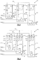
Figure 1 illustrates a highly schematic multi-phase power control switch. -
Figure 2 illustrates a first alternative highly schematic, multi-phase power control switch. -
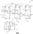
Figure 3 illustrates a second alternative highly schematic multi-phase power control switch. -
Figure 1 illustrates a highly schematic multi-phasepower control switch 10 having three solid-state power controller (SSPC)channels 12a-c. Each of the illustrated SSPC channels 12 includes asingle SSPC 14, although it is understood that additional SSPC's 14 can be included within eachSSPC channel 12a-c. Each of the SSPCs 14 includes amicrocontroller 20, such as a microprocessor. Each of the SSPCs 14 also includes an independent floatingDC power supply 30 providing power to themicrocontroller 20, and anisolator 50 connecting across-communication line 22 of themicrocontroller 20 to adata bus 40. As each of themicrocontrollers 20 is connected to thedata bus 40, cross-communication between eachmicrocontroller 20 and eachother microcontroller 20 over thedata bus 40 is enabled. Each of themicrocontrollers 20 provides control commands 17 to individual power phase switches 16. - To properly cross-communicate between the
microcontrollers 20 and synchronize switching, one of themicrocontrollers 20 is designated as themaster microcontroller 20, and each of theremaining microcontrollers 20 is designated as a slave to themaster microcontroller 20. In the illustrated example ofFigure 1 , themicrocontroller 20 of thecenter SSPC channel 12b is designated the master microcontroller, as indicated by the arrow directions on the connections to thedata bus 40. Thedata bus 40, and the master-slave arrangement, allows the cross-communication and the coordination between each of theSSPC channels 12a-c and each of theSSPCs 14 within eachSSPC channel 12a-c to be done locally between theSSPC channels 12a-c, without the need for a systems level controller to coordinate and synchronize themicrocontrollers 20. Removing the systems level controller increases the response time of the cross-communication and increases the ability to implement timing critical controls within the multi-phasepower control switch 10. This in turn supports synchronization of the controlled removal of power from each of the output power lines 18a, 18b and 18c. - In the absence of a
data bus 40, each of themicrocontrollers 20 must be directly connected to each of theother microcontrollers 20 to enable cross communication between themicrocontrollers 20. Each of the direct connections would require anisolator circuit 50 to prevent the varied reference voltage levels between themicrocontrollers 20 from affecting performance of thepower control switch 10. These different reference levels may be determined by differences of voltage betweenexternal power inputs 11. - In light of the present disclosure, it can be appreciated that practical implementations of the multi-phase
power control switch 10 would incorporateadditional microcontrollers 20 in eachSSPC channel 12a-c or incorporateadditional SSPC channels 12a-c, or both. Incorporation ofadditional microcontrollers 20 orSSPC channels 12a-c results in a geometric increase in the number ofisolators 50 required for cross-communication with eachadditional microcontroller 20 when nodata bus 40 is incorporated. By way of example, adding a single additional microcontroller to a system starting with three microcontrollers would require the addition of three isolators. Contrary to the busless arrangement, the illustratedcross-communication data bus 40 arrangement of the present disclosure only requires a linear increase of a single isolator for eachnew microcontroller 20 incorporated into the switch regardless of the number of microcontrollers currently in the switch. -
Figure 2 illustrates an alternative, highly schematic multi-phasepower control switch 100 having threeSSPC channels 112a-c, each of which has oneSSPC 114. Each of the SSPCs 114 includes aprimary microcontroller 120 andredundant microcontroller 122. Also included in each of theSSPC channels 112a-c of the example ofFigure 2 is anindependent power supply 130 and twoisolators 150, with eachisolator 150 corresponding to one of themicrocontrollers redundant microcontrollers 122 provide backup in case aprimary microcontroller 120 enters a failure state and can no longer provide switching control for the SSPC channel 12. Each of theredundant microcontrollers 122 cross-communicates with each of the otherredundant microcontrollers 122 over aredundant data bus 142. As with theprimary microcontrollers 120, theredundant microcontrollers 122 are connected to theredundant data bus 142 via anisolator 150. Theredundant microcontrollers 122 are connected using the master/slave arrangement described above with regards toFigure 1 . - A further benefit of the local cross-communication between the
microcontrollers data buses redundant microcontroller 122 is only required to communicate with a correspondingprimary microcontroller 120 within thesame power channel 112a-c, and is not required to include cross-communication withprimary microcontrollers 120 outside of thepower channel 112a-c. Eachredundant microcontroller 122 communicates with the correspondingprimary microcontroller 120 and the correspondingprimary microcontroller 120 can communicate any failure mode information through theprimary data bus 140 to each otherprimary microcontroller 120. In this way, a switch to theredundant microcontrollers 122 in each channel of the multi-phase power control switch can be coordinated without requiring eachredundant microcontroller 122 to directly communicate with eachprimary microcontroller 120 or requiring a systems level controller. As communication between theprimary data bus 140 and theredundant data bus 142 occurs betweenmicrocontrollers single SSPC channel 112a-c, noadditional isolators 150 are required. -
Figure 3 illustrates a second alternative highly schematic multi-phasepower control switch 200 including a trip synchronizationsignal capture module 270. Each of the SSPC channels 212a-c are arranged as inFigure 1 with anisolator 250, afloating power supply 230, and amicrocontroller 220. Furthermore, as described above with regards toFigure 1 , adata bus 240 enables cross-communication between themicrocontrollers 220. - A
synchronization bus 242, separate from thedata bus 240, allows themicrocontrollers 220 to receive ground referenced signals from a systems level controller, thereby enabling a systems level controller to monitor thepower control switch 200. As with thecross-communication data bus 240, anisolator 252 is used between themicrocontrollers 220 and thesynchronization bus 242 to prevent the floating reference voltages of thefloating power supplies 230 of each SSPC channel 212a-c from impacting communications between the SSPC channels 212a-c. Also connected to thesynchronization bus 242 is an I/O (input/output) expander 260 and apin input module 290. The I/O expander 260 and thepin input module 290 utilize input pins and jumpers connecting the input pins to program and synchronize themicrocontrollers 220, as well as to interpret the signals from thesynchronization bus 242 for the systems level controller. Thepin input module 290 includes a connection to a system neutral reference voltage (a systems ground 280). - In each of the above-described examples, the
data buses SSPC channels 12a-c, 112a-c, 212a-c and/ormultiple SSPCs Figure 2 andFigure 3 in light of this disclosure. - A power distribution system, such as for an aircraft, includes a plurality of multi-phase power control switches as described above.
- Although embodiments of this invention have been disclosed, these are exemplary only, and a worker of ordinary skill in this art may recognize that certain modifications may come within the scope of this invention. For that reason, the following claims should be studied to determine the true scope and content of this invention.
Claims (9)
- A multi-phase power control switch (10,100,200) comprising:a plurality of power controller channels (12a-c,112a-c,212a-c), each of which includes at least one power controller (14,114,214a-c) having at least one microcontroller (20,120,122,220); andan isolator (50,150,250) corresponding to each of said microcontrollers and connecting a cross communication line (22) of said corresponding microcontroller to a data bus (40,140,142,240), each isolator being configured to prevent varied reference voltage levels between the microcontrollers from affecting performance of the power control switch;said data bus being operable to enable cross communication between each of said microcontrollers and each other of said microcontrollers.
- The multi-phase power control switch of claim 1, wherein at least one of said power controller channels (12a-c,112a-c,212a-c) comprises a plurality of power controllers (14,114,214a-c), each of said power controllers comprising at least one microcontroller (20,120,122,220).
- The multi-phase power control switch of claim 1 or 2, wherein each of said power controller channels (12a-c,112a-c,212a-c) comprises at least one solid state power controller (14,114,214a-c).
- The multi-phase power control switch of claim 3, wherein each of said solid state power controllers (14,114,214a-c), comprises at least a first primary microcontroller (120) and a second redundant microcontroller (122).
- The multi-phase power control switch of claim 4, wherein each of said first primary microcontrollers is connected to a first data bus (140) via the corresponding isolator (150) and wherein each of said second redundant microcontrollers (122) is connected to a second redundant data bus (142) via the corresponding isolator (150).
- The multi-phase power control switch of any preceding claim, further comprising a switch synchronization module (270) having a synchronization bus (242) connected to each of said microcontrollers (220) via a second isolator (252) corresponding to each microcontroller, an input/output (I/O) module (260) connecting said synchronization bus to a pin input module (290), and a system neutral connection (280) connected to said pin input module.
- The multi-phase power control switch of claim 6, wherein said pin input module (290) is operable to program each of said microcontrollers (220) connected to said switch synchronization bus (242), and wherein said pin input module (290) is operable to be programmed via a plurality of jumper connections.
- The multi-phase power control switch of any preceding claim, wherein said data bus (40,140,142,240) is an I2C data bus.
- A power distribution system comprising:
a plurality of multi-phase power control switches as claimed in any preceding claim.
Applications Claiming Priority (2)
| Application Number | Priority Date | Filing Date | Title |
|---|---|---|---|
| US201161566283P | 2011-12-02 | 2011-12-02 | |
| US13/493,220 US9178355B2 (en) | 2011-12-02 | 2012-06-11 | Cross communication arrangement for multiple solid state power controller channels |
Publications (3)
| Publication Number | Publication Date |
|---|---|
| EP2600478A2 EP2600478A2 (en) | 2013-06-05 |
| EP2600478A3 EP2600478A3 (en) | 2017-06-14 |
| EP2600478B1 true EP2600478B1 (en) | 2019-09-18 |
Family
ID=47427224
Family Applications (1)
| Application Number | Title | Priority Date | Filing Date |
|---|---|---|---|
| EP12195363.2A Active EP2600478B1 (en) | 2011-12-02 | 2012-12-03 | Cross communication arrangement for multiple solid state power controller channels |
Country Status (2)
| Country | Link |
|---|---|
| US (1) | US9178355B2 (en) |
| EP (1) | EP2600478B1 (en) |
Families Citing this family (4)
| Publication number | Priority date | Publication date | Assignee | Title |
|---|---|---|---|---|
| US9871448B2 (en) * | 2012-12-31 | 2018-01-16 | Nvidia Corporation | Super N-phase switching mode power supply |
| FR3024927B1 (en) * | 2014-08-14 | 2016-08-26 | Zodiac Aero Electric | ELECTRICAL DISTRIBUTION SYSTEM FOR AN AIRCRAFT |
| US10048997B2 (en) * | 2016-05-04 | 2018-08-14 | Hamilton Sundstrand Corporation | Single event latch up mitigation in solid state power controllers |
| US12271172B2 (en) * | 2021-12-07 | 2025-04-08 | Hamilton Sundstrand Corporation | Solid state power controllers |
Family Cites Families (18)
| Publication number | Priority date | Publication date | Assignee | Title |
|---|---|---|---|---|
| US5761518A (en) * | 1996-02-29 | 1998-06-02 | The Foxboro Company | System for replacing control processor by operating processor in partially disabled mode for tracking control outputs and in write enabled mode for transferring control loops |
| US6470224B1 (en) | 1999-10-01 | 2002-10-22 | Hamilton Sundstrand Corporation | Configurable aircraft power system |
| US6856045B1 (en) | 2002-01-29 | 2005-02-15 | Hamilton Sundstrand Corporation | Power distribution assembly with redundant architecture |
| US7065583B2 (en) * | 2002-02-14 | 2006-06-20 | The Boeing Company | System and associated suppression assembly for limiting electromagnetic emissions in network devices communicating via a network bus |
| US6768350B1 (en) | 2002-04-10 | 2004-07-27 | Hamilton Sundstrand Corporation | Microprocessor based solid state DC power controller |
| US7064448B2 (en) | 2004-09-01 | 2006-06-20 | Hamilton Sundstrand Corporation | Power controller with bond wire fuse |
| US20060071559A1 (en) * | 2004-09-30 | 2006-04-06 | Michael Hanson | Individually and redundantly addressable solid-state power controllers on multiple modules in a power distribution assembly |
| DE602006020027D1 (en) | 2005-02-16 | 2011-03-24 | Leach Int Corp | POWER DISTRIBUTION SYSTEM USING SOLID BODY CONTROLLERS |
| US7505820B2 (en) | 2006-03-30 | 2009-03-17 | Honeywell International Inc. | Backup control for solid state power controller (SSPC) |
| US7656634B2 (en) * | 2006-11-30 | 2010-02-02 | Hamilton Sundstrand Corporation | Increasing the system stability and lightning capability in a power distribution system that utilizes solid-state power controllers |
| US7363129B1 (en) * | 2007-01-05 | 2008-04-22 | Moon Valley Software | Apparatus, system and method that interfaces with an automobile engine control unit |
| US7634329B2 (en) * | 2007-03-05 | 2009-12-15 | Honeywell International Inc. | Intelligent aircraft secondary power distribution system that facilitates condition based maintenance |
| US8050806B2 (en) * | 2007-03-21 | 2011-11-01 | Honeywell International Inc. | Ground fault interruption using DSP based SSPC module |
| US8148848B2 (en) | 2008-01-24 | 2012-04-03 | Honeywell International, Inc. | Solid state power controller (SSPC) used as bus tie breaker in electrical power distribution systems |
| US7626798B2 (en) * | 2008-01-24 | 2009-12-01 | Honeywell International Inc. | Electronic load control unit (ELCU) used as bus tie breaker in electrical power distribution systems |
| US8031451B2 (en) | 2009-01-06 | 2011-10-04 | Hamilton Sundstrand Corporation | Solid state power control module with removal detector |
| FR2941338B1 (en) | 2009-01-20 | 2016-11-04 | Crouzet Automatismes | HIGH VOLTAGE STATIC SWITCH |
| US8023236B2 (en) * | 2009-03-18 | 2011-09-20 | Hamilton Sundstrand Corporation | Precision ground fault detection for aircraft human body protection |
-
2012
- 2012-06-11 US US13/493,220 patent/US9178355B2/en active Active
- 2012-12-03 EP EP12195363.2A patent/EP2600478B1/en active Active
Non-Patent Citations (1)
| Title |
|---|
| None * |
Also Published As
| Publication number | Publication date |
|---|---|
| EP2600478A2 (en) | 2013-06-05 |
| US9178355B2 (en) | 2015-11-03 |
| US20130144447A1 (en) | 2013-06-06 |
| EP2600478A3 (en) | 2017-06-14 |
Similar Documents
| Publication | Publication Date | Title |
|---|---|---|
| US8760004B2 (en) | Electrical power distribution | |
| EP2639918B1 (en) | Control architecture for power switching controller | |
| US7816813B2 (en) | Method and apparatus for parallel engine generators | |
| EP2619871B1 (en) | Aircraft power distribution network | |
| EP2573636B1 (en) | Multi-channel control switchover logic | |
| EP1973018B1 (en) | Integrated electrical power distribution system using common building blocks | |
| US7020790B2 (en) | Electric load management center including gateway module and multiple load management modules for distributing power to multiple loads | |
| US20050036253A1 (en) | Modular AC power supply system with fault bypass and method of switching output modes | |
| US9178355B2 (en) | Cross communication arrangement for multiple solid state power controller channels | |
| US9342414B1 (en) | Reserve power bus ring for data center | |
| CN105373031B (en) | System and method for controlling at least one switching device, in particular for use in an aircraft | |
| EP2156533A1 (en) | Transfer switch system with neutral current management | |
| CN104536321A (en) | System and method for achieving power failure detection and relay state control | |
| US20120235480A1 (en) | Uninterrupted power supply system and uninterrupted power supply device | |
| EP3626505A1 (en) | A system and method for providing redundant electric power | |
| CA2735985C (en) | Redundant power supply | |
| CN108701991B (en) | Power distribution device comprising at least one power controller | |
| EP2801874B1 (en) | Multi-channel control switchover logic | |
| EP3626543B1 (en) | A protection circuitry and a method for protecting a vehicle power supply | |
| CN105226810A (en) | Many ups systems power supply synchronization system and method | |
| JP3047458B2 (en) | System switching device for uninterruptible power supply system | |
| EP2595268B1 (en) | Minimal interruption DC power supply | |
| JP4808204B2 (en) | Power external input / output device | |
| JPH0226222A (en) | Distribution line protection relay device and distribution line device | |
| EP4052350B1 (en) | Uninterruptible power supply system having stranded power recovery |
Legal Events
| Date | Code | Title | Description |
|---|---|---|---|
| PUAI | Public reference made under article 153(3) epc to a published international application that has entered the european phase |
Free format text: ORIGINAL CODE: 0009012 |
|
| AK | Designated contracting states |
Kind code of ref document: A2 Designated state(s): AL AT BE BG CH CY CZ DE DK EE ES FI FR GB GR HR HU IE IS IT LI LT LU LV MC MK MT NL NO PL PT RO RS SE SI SK SM TR |
|
| AX | Request for extension of the european patent |
Extension state: BA ME |
|
| PUAL | Search report despatched |
Free format text: ORIGINAL CODE: 0009013 |
|
| AK | Designated contracting states |
Kind code of ref document: A3 Designated state(s): AL AT BE BG CH CY CZ DE DK EE ES FI FR GB GR HR HU IE IS IT LI LT LU LV MC MK MT NL NO PL PT RO RS SE SI SK SM TR |
|
| AX | Request for extension of the european patent |
Extension state: BA ME |
|
| RIC1 | Information provided on ipc code assigned before grant |
Ipc: H02J 13/00 20060101ALI20170508BHEP Ipc: H02J 3/26 20060101AFI20170508BHEP Ipc: H04L 12/40 20060101ALI20170508BHEP |
|
| STAA | Information on the status of an ep patent application or granted ep patent |
Free format text: STATUS: REQUEST FOR EXAMINATION WAS MADE |
|
| 17P | Request for examination filed |
Effective date: 20171214 |
|
| RBV | Designated contracting states (corrected) |
Designated state(s): AL AT BE BG CH CY CZ DE DK EE ES FI FR GB GR HR HU IE IS IT LI LT LU LV MC MK MT NL NO PL PT RO RS SE SI SK SM TR |
|
| RAP1 | Party data changed (applicant data changed or rights of an application transferred) |
Owner name: HAMILTON SUNDSTRAND CORPORATION |
|
| GRAP | Despatch of communication of intention to grant a patent |
Free format text: ORIGINAL CODE: EPIDOSNIGR1 |
|
| STAA | Information on the status of an ep patent application or granted ep patent |
Free format text: STATUS: GRANT OF PATENT IS INTENDED |
|
| INTG | Intention to grant announced |
Effective date: 20190401 |
|
| GRAS | Grant fee paid |
Free format text: ORIGINAL CODE: EPIDOSNIGR3 |
|
| GRAA | (expected) grant |
Free format text: ORIGINAL CODE: 0009210 |
|
| STAA | Information on the status of an ep patent application or granted ep patent |
Free format text: STATUS: THE PATENT HAS BEEN GRANTED |
|
| AK | Designated contracting states |
Kind code of ref document: B1 Designated state(s): AL AT BE BG CH CY CZ DE DK EE ES FI FR GB GR HR HU IE IS IT LI LT LU LV MC MK MT NL NO PL PT RO RS SE SI SK SM TR |
|
| REG | Reference to a national code |
Ref country code: GB Ref legal event code: FG4D |
|
| REG | Reference to a national code |
Ref country code: CH Ref legal event code: EP |
|
| REG | Reference to a national code |
Ref country code: DE Ref legal event code: R096 Ref document number: 602012064064 Country of ref document: DE |
|
| REG | Reference to a national code |
Ref country code: AT Ref legal event code: REF Ref document number: 1182440 Country of ref document: AT Kind code of ref document: T Effective date: 20191015 |
|
| REG | Reference to a national code |
Ref country code: IE Ref legal event code: FG4D |
|
| REG | Reference to a national code |
Ref country code: NL Ref legal event code: MP Effective date: 20190918 |
|
| PG25 | Lapsed in a contracting state [announced via postgrant information from national office to epo] |
Ref country code: FI Free format text: LAPSE BECAUSE OF FAILURE TO SUBMIT A TRANSLATION OF THE DESCRIPTION OR TO PAY THE FEE WITHIN THE PRESCRIBED TIME-LIMIT Effective date: 20190918 Ref country code: BG Free format text: LAPSE BECAUSE OF FAILURE TO SUBMIT A TRANSLATION OF THE DESCRIPTION OR TO PAY THE FEE WITHIN THE PRESCRIBED TIME-LIMIT Effective date: 20191218 Ref country code: SE Free format text: LAPSE BECAUSE OF FAILURE TO SUBMIT A TRANSLATION OF THE DESCRIPTION OR TO PAY THE FEE WITHIN THE PRESCRIBED TIME-LIMIT Effective date: 20190918 Ref country code: NO Free format text: LAPSE BECAUSE OF FAILURE TO SUBMIT A TRANSLATION OF THE DESCRIPTION OR TO PAY THE FEE WITHIN THE PRESCRIBED TIME-LIMIT Effective date: 20191218 Ref country code: HR Free format text: LAPSE BECAUSE OF FAILURE TO SUBMIT A TRANSLATION OF THE DESCRIPTION OR TO PAY THE FEE WITHIN THE PRESCRIBED TIME-LIMIT Effective date: 20190918 Ref country code: LT Free format text: LAPSE BECAUSE OF FAILURE TO SUBMIT A TRANSLATION OF THE DESCRIPTION OR TO PAY THE FEE WITHIN THE PRESCRIBED TIME-LIMIT Effective date: 20190918 |
|
| REG | Reference to a national code |
Ref country code: LT Ref legal event code: MG4D |
|
| PG25 | Lapsed in a contracting state [announced via postgrant information from national office to epo] |
Ref country code: AL Free format text: LAPSE BECAUSE OF FAILURE TO SUBMIT A TRANSLATION OF THE DESCRIPTION OR TO PAY THE FEE WITHIN THE PRESCRIBED TIME-LIMIT Effective date: 20190918 Ref country code: GR Free format text: LAPSE BECAUSE OF FAILURE TO SUBMIT A TRANSLATION OF THE DESCRIPTION OR TO PAY THE FEE WITHIN THE PRESCRIBED TIME-LIMIT Effective date: 20191219 Ref country code: LV Free format text: LAPSE BECAUSE OF FAILURE TO SUBMIT A TRANSLATION OF THE DESCRIPTION OR TO PAY THE FEE WITHIN THE PRESCRIBED TIME-LIMIT Effective date: 20190918 Ref country code: RS Free format text: LAPSE BECAUSE OF FAILURE TO SUBMIT A TRANSLATION OF THE DESCRIPTION OR TO PAY THE FEE WITHIN THE PRESCRIBED TIME-LIMIT Effective date: 20190918 |
|
| REG | Reference to a national code |
Ref country code: AT Ref legal event code: MK05 Ref document number: 1182440 Country of ref document: AT Kind code of ref document: T Effective date: 20190918 |
|
| PG25 | Lapsed in a contracting state [announced via postgrant information from national office to epo] |
Ref country code: RO Free format text: LAPSE BECAUSE OF FAILURE TO SUBMIT A TRANSLATION OF THE DESCRIPTION OR TO PAY THE FEE WITHIN THE PRESCRIBED TIME-LIMIT Effective date: 20190918 Ref country code: NL Free format text: LAPSE BECAUSE OF FAILURE TO SUBMIT A TRANSLATION OF THE DESCRIPTION OR TO PAY THE FEE WITHIN THE PRESCRIBED TIME-LIMIT Effective date: 20190918 Ref country code: PL Free format text: LAPSE BECAUSE OF FAILURE TO SUBMIT A TRANSLATION OF THE DESCRIPTION OR TO PAY THE FEE WITHIN THE PRESCRIBED TIME-LIMIT Effective date: 20190918 Ref country code: ES Free format text: LAPSE BECAUSE OF FAILURE TO SUBMIT A TRANSLATION OF THE DESCRIPTION OR TO PAY THE FEE WITHIN THE PRESCRIBED TIME-LIMIT Effective date: 20190918 Ref country code: AT Free format text: LAPSE BECAUSE OF FAILURE TO SUBMIT A TRANSLATION OF THE DESCRIPTION OR TO PAY THE FEE WITHIN THE PRESCRIBED TIME-LIMIT Effective date: 20190918 Ref country code: PT Free format text: LAPSE BECAUSE OF FAILURE TO SUBMIT A TRANSLATION OF THE DESCRIPTION OR TO PAY THE FEE WITHIN THE PRESCRIBED TIME-LIMIT Effective date: 20200120 Ref country code: EE Free format text: LAPSE BECAUSE OF FAILURE TO SUBMIT A TRANSLATION OF THE DESCRIPTION OR TO PAY THE FEE WITHIN THE PRESCRIBED TIME-LIMIT Effective date: 20190918 Ref country code: IT Free format text: LAPSE BECAUSE OF FAILURE TO SUBMIT A TRANSLATION OF THE DESCRIPTION OR TO PAY THE FEE WITHIN THE PRESCRIBED TIME-LIMIT Effective date: 20190918 |
|
| PG25 | Lapsed in a contracting state [announced via postgrant information from national office to epo] |
Ref country code: SK Free format text: LAPSE BECAUSE OF FAILURE TO SUBMIT A TRANSLATION OF THE DESCRIPTION OR TO PAY THE FEE WITHIN THE PRESCRIBED TIME-LIMIT Effective date: 20190918 Ref country code: CZ Free format text: LAPSE BECAUSE OF FAILURE TO SUBMIT A TRANSLATION OF THE DESCRIPTION OR TO PAY THE FEE WITHIN THE PRESCRIBED TIME-LIMIT Effective date: 20190918 Ref country code: SM Free format text: LAPSE BECAUSE OF FAILURE TO SUBMIT A TRANSLATION OF THE DESCRIPTION OR TO PAY THE FEE WITHIN THE PRESCRIBED TIME-LIMIT Effective date: 20190918 Ref country code: IS Free format text: LAPSE BECAUSE OF FAILURE TO SUBMIT A TRANSLATION OF THE DESCRIPTION OR TO PAY THE FEE WITHIN THE PRESCRIBED TIME-LIMIT Effective date: 20200224 |
|
| REG | Reference to a national code |
Ref country code: DE Ref legal event code: R097 Ref document number: 602012064064 Country of ref document: DE |
|
| PLBE | No opposition filed within time limit |
Free format text: ORIGINAL CODE: 0009261 |
|
| STAA | Information on the status of an ep patent application or granted ep patent |
Free format text: STATUS: NO OPPOSITION FILED WITHIN TIME LIMIT |
|
| PG2D | Information on lapse in contracting state deleted |
Ref country code: IS |
|
| PG25 | Lapsed in a contracting state [announced via postgrant information from national office to epo] |
Ref country code: DK Free format text: LAPSE BECAUSE OF FAILURE TO SUBMIT A TRANSLATION OF THE DESCRIPTION OR TO PAY THE FEE WITHIN THE PRESCRIBED TIME-LIMIT Effective date: 20190918 Ref country code: IS Free format text: LAPSE BECAUSE OF FAILURE TO SUBMIT A TRANSLATION OF THE DESCRIPTION OR TO PAY THE FEE WITHIN THE PRESCRIBED TIME-LIMIT Effective date: 20200119 |
|
| REG | Reference to a national code |
Ref country code: CH Ref legal event code: PL |
|
| 26N | No opposition filed |
Effective date: 20200619 |
|
| REG | Reference to a national code |
Ref country code: BE Ref legal event code: MM Effective date: 20191231 |
|
| PG25 | Lapsed in a contracting state [announced via postgrant information from national office to epo] |
Ref country code: MC Free format text: LAPSE BECAUSE OF FAILURE TO SUBMIT A TRANSLATION OF THE DESCRIPTION OR TO PAY THE FEE WITHIN THE PRESCRIBED TIME-LIMIT Effective date: 20190918 Ref country code: SI Free format text: LAPSE BECAUSE OF FAILURE TO SUBMIT A TRANSLATION OF THE DESCRIPTION OR TO PAY THE FEE WITHIN THE PRESCRIBED TIME-LIMIT Effective date: 20190918 |
|
| PG25 | Lapsed in a contracting state [announced via postgrant information from national office to epo] |
Ref country code: LU Free format text: LAPSE BECAUSE OF NON-PAYMENT OF DUE FEES Effective date: 20191203 Ref country code: IE Free format text: LAPSE BECAUSE OF NON-PAYMENT OF DUE FEES Effective date: 20191203 |
|
| PG25 | Lapsed in a contracting state [announced via postgrant information from national office to epo] |
Ref country code: BE Free format text: LAPSE BECAUSE OF NON-PAYMENT OF DUE FEES Effective date: 20191231 Ref country code: LI Free format text: LAPSE BECAUSE OF NON-PAYMENT OF DUE FEES Effective date: 20191231 Ref country code: CH Free format text: LAPSE BECAUSE OF NON-PAYMENT OF DUE FEES Effective date: 20191231 |
|
| PG25 | Lapsed in a contracting state [announced via postgrant information from national office to epo] |
Ref country code: CY Free format text: LAPSE BECAUSE OF FAILURE TO SUBMIT A TRANSLATION OF THE DESCRIPTION OR TO PAY THE FEE WITHIN THE PRESCRIBED TIME-LIMIT Effective date: 20190918 |
|
| PG25 | Lapsed in a contracting state [announced via postgrant information from national office to epo] |
Ref country code: MT Free format text: LAPSE BECAUSE OF FAILURE TO SUBMIT A TRANSLATION OF THE DESCRIPTION OR TO PAY THE FEE WITHIN THE PRESCRIBED TIME-LIMIT Effective date: 20190918 Ref country code: HU Free format text: LAPSE BECAUSE OF FAILURE TO SUBMIT A TRANSLATION OF THE DESCRIPTION OR TO PAY THE FEE WITHIN THE PRESCRIBED TIME-LIMIT; INVALID AB INITIO Effective date: 20121203 |
|
| PG25 | Lapsed in a contracting state [announced via postgrant information from national office to epo] |
Ref country code: TR Free format text: LAPSE BECAUSE OF FAILURE TO SUBMIT A TRANSLATION OF THE DESCRIPTION OR TO PAY THE FEE WITHIN THE PRESCRIBED TIME-LIMIT Effective date: 20190918 |
|
| PG25 | Lapsed in a contracting state [announced via postgrant information from national office to epo] |
Ref country code: MK Free format text: LAPSE BECAUSE OF FAILURE TO SUBMIT A TRANSLATION OF THE DESCRIPTION OR TO PAY THE FEE WITHIN THE PRESCRIBED TIME-LIMIT Effective date: 20190918 |
|
| P01 | Opt-out of the competence of the unified patent court (upc) registered |
Effective date: 20230522 |
|
| PGFP | Annual fee paid to national office [announced via postgrant information from national office to epo] |
Ref country code: DE Payment date: 20251126 Year of fee payment: 14 |
|
| PGFP | Annual fee paid to national office [announced via postgrant information from national office to epo] |
Ref country code: GB Payment date: 20251120 Year of fee payment: 14 |
|
| PGFP | Annual fee paid to national office [announced via postgrant information from national office to epo] |
Ref country code: FR Payment date: 20251120 Year of fee payment: 14 |